JP3850600B2 - Information recording disk and information recording apparatus - Google Patents
Information recording disk and information recording apparatus Download PDFInfo
- Publication number
- JP3850600B2 JP3850600B2 JP29381499A JP29381499A JP3850600B2 JP 3850600 B2 JP3850600 B2 JP 3850600B2 JP 29381499 A JP29381499 A JP 29381499A JP 29381499 A JP29381499 A JP 29381499A JP 3850600 B2 JP3850600 B2 JP 3850600B2
- Authority
- JP
- Japan
- Prior art keywords
- recording
- information
- signal
- wobble
- phase
- Prior art date
- Legal status (The legal status is an assumption and is not a legal conclusion. Google has not performed a legal analysis and makes no representation as to the accuracy of the status listed.)
- Expired - Lifetime
Links
Images


Classifications
-
- H—ELECTRICITY
- H04—ELECTRIC COMMUNICATION TECHNIQUE
- H04L—TRANSMISSION OF DIGITAL INFORMATION, e.g. TELEGRAPHIC COMMUNICATION
- H04L27/00—Modulated-carrier systems
- H04L27/18—Phase-modulated carrier systems, i.e. using phase-shift keying
- H04L27/22—Demodulator circuits; Receiver circuits
- H04L27/227—Demodulator circuits; Receiver circuits using coherent demodulation
- H04L27/2271—Demodulator circuits; Receiver circuits using coherent demodulation wherein the carrier recovery circuit uses only the demodulated signals
- H04L27/2273—Demodulator circuits; Receiver circuits using coherent demodulation wherein the carrier recovery circuit uses only the demodulated signals associated with quadrature demodulation, e.g. Costas loop
-
- G—PHYSICS
- G11—INFORMATION STORAGE
- G11B—INFORMATION STORAGE BASED ON RELATIVE MOVEMENT BETWEEN RECORD CARRIER AND TRANSDUCER
- G11B20/00—Signal processing not specific to the method of recording or reproducing; Circuits therefor
- G11B20/10—Digital recording or reproducing
- G11B20/14—Digital recording or reproducing using self-clocking codes
- G11B20/1403—Digital recording or reproducing using self-clocking codes characterised by the use of two levels
-
- G—PHYSICS
- G11—INFORMATION STORAGE
- G11B—INFORMATION STORAGE BASED ON RELATIVE MOVEMENT BETWEEN RECORD CARRIER AND TRANSDUCER
- G11B27/00—Editing; Indexing; Addressing; Timing or synchronising; Monitoring; Measuring tape travel
- G11B27/02—Editing, e.g. varying the order of information signals recorded on, or reproduced from, record carriers
- G11B27/031—Electronic editing of digitised analogue information signals, e.g. audio or video signals
- G11B27/034—Electronic editing of digitised analogue information signals, e.g. audio or video signals on discs
-
- G—PHYSICS
- G11—INFORMATION STORAGE
- G11B—INFORMATION STORAGE BASED ON RELATIVE MOVEMENT BETWEEN RECORD CARRIER AND TRANSDUCER
- G11B27/00—Editing; Indexing; Addressing; Timing or synchronising; Monitoring; Measuring tape travel
- G11B27/10—Indexing; Addressing; Timing or synchronising; Measuring tape travel
- G11B27/19—Indexing; Addressing; Timing or synchronising; Measuring tape travel by using information detectable on the record carrier
- G11B27/24—Indexing; Addressing; Timing or synchronising; Measuring tape travel by using information detectable on the record carrier by sensing features on the record carrier other than the transducing track ; sensing signals or marks recorded by another method than the main recording
-
- G—PHYSICS
- G11—INFORMATION STORAGE
- G11B—INFORMATION STORAGE BASED ON RELATIVE MOVEMENT BETWEEN RECORD CARRIER AND TRANSDUCER
- G11B27/00—Editing; Indexing; Addressing; Timing or synchronising; Monitoring; Measuring tape travel
- G11B27/10—Indexing; Addressing; Timing or synchronising; Measuring tape travel
- G11B27/19—Indexing; Addressing; Timing or synchronising; Measuring tape travel by using information detectable on the record carrier
- G11B27/28—Indexing; Addressing; Timing or synchronising; Measuring tape travel by using information detectable on the record carrier by using information signals recorded by the same method as the main recording
- G11B27/30—Indexing; Addressing; Timing or synchronising; Measuring tape travel by using information detectable on the record carrier by using information signals recorded by the same method as the main recording on the same track as the main recording
- G11B27/3027—Indexing; Addressing; Timing or synchronising; Measuring tape travel by using information detectable on the record carrier by using information signals recorded by the same method as the main recording on the same track as the main recording used signal is digitally coded
-
- G—PHYSICS
- G11—INFORMATION STORAGE
- G11B—INFORMATION STORAGE BASED ON RELATIVE MOVEMENT BETWEEN RECORD CARRIER AND TRANSDUCER
- G11B7/00—Recording or reproducing by optical means, e.g. recording using a thermal beam of optical radiation by modifying optical properties or the physical structure, reproducing using an optical beam at lower power by sensing optical properties; Record carriers therefor
- G11B7/007—Arrangement of the information on the record carrier, e.g. form of tracks, actual track shape, e.g. wobbled, or cross-section, e.g. v-shaped; Sequential information structures, e.g. sectoring or header formats within a track
-
- G—PHYSICS
- G11—INFORMATION STORAGE
- G11B—INFORMATION STORAGE BASED ON RELATIVE MOVEMENT BETWEEN RECORD CARRIER AND TRANSDUCER
- G11B2220/00—Record carriers by type
- G11B2220/20—Disc-shaped record carriers
- G11B2220/21—Disc-shaped record carriers characterised in that the disc is of read-only, rewritable, or recordable type
- G11B2220/215—Recordable discs
- G11B2220/216—Rewritable discs
-
- G—PHYSICS
- G11—INFORMATION STORAGE
- G11B—INFORMATION STORAGE BASED ON RELATIVE MOVEMENT BETWEEN RECORD CARRIER AND TRANSDUCER
- G11B2220/00—Record carriers by type
- G11B2220/20—Disc-shaped record carriers
- G11B2220/21—Disc-shaped record carriers characterised in that the disc is of read-only, rewritable, or recordable type
- G11B2220/215—Recordable discs
- G11B2220/218—Write-once discs
-
- G—PHYSICS
- G11—INFORMATION STORAGE
- G11B—INFORMATION STORAGE BASED ON RELATIVE MOVEMENT BETWEEN RECORD CARRIER AND TRANSDUCER
- G11B2220/00—Record carriers by type
- G11B2220/20—Disc-shaped record carriers
- G11B2220/25—Disc-shaped record carriers characterised in that the disc is based on a specific recording technology
- G11B2220/2537—Optical discs
- G11B2220/2545—CDs
-
- G—PHYSICS
- G11—INFORMATION STORAGE
- G11B—INFORMATION STORAGE BASED ON RELATIVE MOVEMENT BETWEEN RECORD CARRIER AND TRANSDUCER
- G11B2220/00—Record carriers by type
- G11B2220/20—Disc-shaped record carriers
- G11B2220/25—Disc-shaped record carriers characterised in that the disc is based on a specific recording technology
- G11B2220/2537—Optical discs
- G11B2220/2562—DVDs [digital versatile discs]; Digital video discs; MMCDs; HDCDs
- G11B2220/2575—DVD-RAMs
-
- H—ELECTRICITY
- H04—ELECTRIC COMMUNICATION TECHNIQUE
- H04L—TRANSMISSION OF DIGITAL INFORMATION, e.g. TELEGRAPHIC COMMUNICATION
- H04L27/00—Modulated-carrier systems
- H04L27/0014—Carrier regulation
- H04L2027/0024—Carrier regulation at the receiver end
- H04L2027/0026—Correction of carrier offset
- H04L2027/0028—Correction of carrier offset at passband only
-
- H—ELECTRICITY
- H04—ELECTRIC COMMUNICATION TECHNIQUE
- H04L—TRANSMISSION OF DIGITAL INFORMATION, e.g. TELEGRAPHIC COMMUNICATION
- H04L27/00—Modulated-carrier systems
- H04L27/0014—Carrier regulation
- H04L2027/0044—Control loops for carrier regulation
- H04L2027/0053—Closed loops
- H04L2027/0057—Closed loops quadrature phase
Landscapes
- Engineering & Computer Science (AREA)
- Signal Processing (AREA)
- Multimedia (AREA)
- Computer Networks & Wireless Communication (AREA)
- Optical Recording Or Reproduction (AREA)
- Optical Record Carriers And Manufacture Thereof (AREA)
Description
【0001】
【発明の属する技術分野】
本発明は、情報の記録に用いられる光ディスク等の情報記録ディスクに関し、特に、ウォブル(wobbling)が形成された記録トラックを有し、情報の追記、書き換えが可能な情報記録ディスクに関する。さらに、本発明は、このような情報記録ディスクに情報を記録する情報記録装置に関する。
【0002】
【従来の技術】
情報を1回だけ記録可能なCD(Compact Disk)は、CD−R(CD-Recordable)として一般に知られている。また、情報を多数回書き換え可能なCDは、CD−RW(CD-ReWritable)として一般に知られている。これらCD−RおよびCD−RWの記録トラックは、半径方向に微小に蛇行している。この記録トラックの蛇行は一般にウォブル(wobbling)と呼ばれている。
【0003】
一方、ディスクに情報を記録するため、または、ディスク上に記録された情報を再生するためには、ディスク上における絶対アドレス(または絶対時間)を示す情報が必要である。以下、この情報をプリ情報と呼ぶ。
【0004】
CD−RおよびCD−RWにおいて、プリ情報は、ウォブルをFM変調させることによってディスク上に記録される。具体的には、ウォブル形成に用いられるキャリア信号をプリ情報によってFM変調し、このFM変調されたキャリア信号の波形に対応したウォブルを記録トラックに形成する。これにより、プリ情報がディスク上に記録される。
【0005】
【発明が解決しようとする課題】
ところで、CD−RまたはCD−RWに情報を記録するとき、または、CD−RまたはCD−RWに記録された情報を再生するとき、記録装置または再生装置は、CD−RまたはCD−RWに形成されたウォブルを読み取り、このウォブルから得られる情報に基づいて、CD−RまたはCD−RWの回転数制御や記録クロックの生成を行う。このため、ウォブルの周波数が大きく変化することは好ましくない。従って、プリ情報をウォブルに重畳するためにウォブルの周波数を変化させることが許される量はわずかである。例えば、ウォブルの周波数が22.05kHzの場合、プリ情報を重畳するためにウォブルの周波数を変化させる量はわずか±1kHzである。この結果、記録装置または再生装置によって、ウォブルからプリ情報を正確に検出するのは容易でなく、このため、ディスク上の位置を特定する精度が低いという問題がある。
【0006】
ディスク上の位置を特定する精度が低いと、ディスク上に既に記録された記録情報に続けて新たな記録情報を追記(リンキング)するとき、記録位置のずれが生じやすい。この結果、例えば、既記録情報上に新記録情報が上書きされたり、既記録情報と新記録情報との間に予測不能な隙間が生じる場合がある。このような事態を避けるために、CD−RおよびCD−RWでは、記録情報の書込終了時に、この記録情報に続けてダミーデータを記録することによってバッファ領域を確保している。しかしながら、このバッファ領域はディスクの記憶容量の損失を招くという欠点がある。
【0007】
一方、DVD−RAM等の記録可能なDVDでは、CD−RおよびCD−RWと異なる方法を用いて、プリ情報のディスクへの記録を実現している。即ち、記録可能なDVDでは、プリピット(エンボスピット)をディスク上に形成することにより、プリ情報をディスク上に記録する方法を採用している。
【0008】
しかし、この方法では、記録可能なDVDにだけプリピットを設けるという構成上、再生専用のディスクと記録可能なディスクとの間で構造上の相違が大きくなる。このため、両者の互換性を図ることが難しい。例えば、プリピットを有する記録可能なディスク上に記録された情報の再生と、プリピットを有しない再生専用ディスク上に記録された情報の再生とを共通の再生手段で行うことが困難になるという問題がある。
【0009】
本発明はこのような問題に鑑みなされたものであり、本発明の課題は、再生専用の記録ディスクと記録可能な記録ディスクとの間で互換性を容易に図ることができ、かつ、ディスク上における記録情報の記録位置を容易かつ正確に検出することができる情報記録ディスクを提供することにある。さらに、本発明の課題は、ディスク上における記録情報の記録位置を容易かつ正確に検出することができる情報記録装置を提供することにある。
【0010】
【課題を解決するための手段】
上記課題を解決するために、請求項1に記載の発明は、ディスク面上に設けられ再生すべき記録情報を記録するためのトラックと、前記トラックに設けられ複数の箇所で位相が変化するウォブルとを備え、前記ディスク面上における位置を示す位置情報が複数の前記ウォブルの同位相の一群として記録された情報記録ディスクであって、前記記録情報は、所定の配置周期で配置され、当該記録情報の記録または再生の際に同期をとるための同期信号を含んでおり、前記記録情報が前記トラック上に記録されたときに、前記トラック上における前記一群の開始位置の間隔が、前記同期信号の配置周期のN倍(Nは1以上の整数)である情報記録ディスクに前記記録情報を記録する情報記録装置であって、前記ウォブルに対応したウォブル信号を前記情報記録ディスクから検出するウォブル検出手段と、前記ウォブル信号の位相を検出し、前記ウォブル信号の位相の変化を示す検出信号を生成する位相検出手段と、前記検出信号に基づいて前記位置情報を復調する位置情報復調手段と、を備える。
【0011】
上記の課題を解決するために、請求項4に記載の発明は、ディスク面上に設けられ再生すべき記録情報を記録するためのトラックと、前記トラックに設けられ複数の箇所で位相が変化するウォブルとを備え、前記ディスク面上における位置を示す位置情報が複数の前記ウォブルの同位相の一群として記録された情報記録ディスクに前記記録情報を記録する情報記録方法であって、前記ウォブルに対応したウォブル信号を前記情報記録ディスクから検出するウォブル検出工程と、前記ウォブル信号の位相を検出し、前記ウォブル信号の位相の変化を示す検出信号を生成する位相検出工程と、前記検出信号に基づいて前記位置情報を復調する位置情報復調工程と、前記ウォブル信号の同位相の一群の開始位置の間隔が、前記記録情報における同期信号の配置周期のN倍(Nは1以上の整数)に相当するように、前記記録情報を前記情報記録ディスクに記録する記録工程と、を含む。
【0023】
【発明の実施の形態】
以下、本発明の実施の形態を添付図面に従って説明する。
I.光ディスク
まず、光ディスクについて説明する。図1は、本発明の実施形態による情報記録ディスクとしての光ディスク1を示している。光ディスク1は、CD−RまたはDVD−Rとほぼ同様の半径および厚さを有するディスクである。光ディスク1は、記録データをその上に記録することができる記録ディスクであり、記録データを1度または何度も書き換えることができる追記型または書換可能型のディスクである。光ディスク1は、記録データが一切、または、特別な制御情報を除いて一切記録されていない状態のいわゆる空ディスクとして販売されることを想定している。そして、記録データの記録は、光ディスク1を購入したユーザ等の意思に基づき、後述する記録再生装置70によって行われることを想定している。
【0024】
図1に示すように、光ディスク1の少なくとも一方のディスク面3には、グルーブトラック5およびランドトラック7が形成されている。グルーブトラック5は、記録データを記録するためのトラックである。記録データは、再生、編集、保管、配布等を目的としてディスクに記録するためのデータであり、例えば、音楽データ、映像データ、コンピュータプログラム、再生装置を制御するための制御データ、当該ディスクに記録されたデータを管理するデータを含む。記録データは、グルーブトラック5上にピット列として記録される。
【0025】
ランドトラック7は、記録データの記録または読み出しを行うための光ビームを誘導するためのトラックである。
【0026】
グルーブトラック5およびランドトラック7は、光ディスク1の中心を基準にして螺旋状または同心円状に伸長している。また、グルーブトラック5およびランドトラック7は、光ディスク1の半径方向に交互に配置されている。
【0027】
なお、従来のDVD−RAMにはディスク面上にプリピットが形成されているが、本実施形態における光ディスク1のディスク面3上にはプリピットは形成されていない。
【0028】
図2は、光ディスク1のグルーブトラック5およびランドトラック7を部分的に拡大して示している。図2に示すように、グルーブトラック5にはウォブル(wobbling)6が形成されている。ウォブル6は、グルーブトラック5を光ディスク1の半径方向に蛇行させることによって形成されている。本実施形態では、グルーブトラック5が蛇行する周波数は一定である。以下、グルーブトラック5が蛇行する周波数を「ウォブル周波数」という。
【0029】
ウォブル6は、プリ情報をグルーブトラック5の蛇行によってディスク上に記録したものである。プリ情報とは、光ディスク1の絶対アドレス(または、絶対時間)を示す情報である。以下、光ディスク1上の絶対アドレスを「プリアドレス」という。プリ情報は、2ビットのデジタルデータである。本実施形態では、プリ情報が「1」か「0」かに応じて、一定の周期で振動するウォブル6の位相を反転させることにより、プリ情報の光ディスク1上への記録を実現している。
【0030】
なお、ウォブル6は、光ディスク1の物理的構造の一部として、光ディスク1の製造段階で形成される。即ち、ウォブル6として記録されるプリ情報は、光ディスク1の製造段階で光ディスク1上に記録される。ウォブル6の形成、即ち、プリ情報の光ディスク1への記録は、ディスク製造装置50(図10)によって行われる。
【0031】
これに対し、記録データは、光ディスク1の製造段階で記録されるものではない。記録データは、光ディスク1が販売された後、ユーザの自由意思等に基づいき、記録再生装置70によって記録されるものである。
【0032】
次に、記録データの構造について説明する。図3は記録データの構造(記録フォーマット)を示している。本実施形態による光ディスク1は、従来のDVDとほぼ同様の記録データ構造を採用している。図3に示すように、記録データは、複数のセクタ11に分割されている。各セクタ11は、複数のシンクフレーム15に分割されている。各シンクフレーム15は、シンクパターン19と記録データ17からなり、シンクパターン19は、各シンクフレーム15の先頭に位置している。
【0033】
さらに具体的に説明すると、各セクタ11は、26個のシンクフレーム15(シンクフレーム0〜25)に分割されており、各シンクフレーム15のサイズは93バイトである。また、連続して配置された16個のセクタ11(セクタ0〜15)によりECC(Error Correction Code)ブロック13が構成される。ECCブロック13とは、記録データの再生時におけるエラー訂正処理の単位ブロックである。
【0034】
シンクパターン19は、隣接するシンクフレーム15間の境界を示すデータである。そして、シンクパターン19は、記録データの記録または再生の際に同期をとるための同期信号として機能する。シンクパターン19は、常にシンクフレーム15の先頭に配置されるため、記録データを全体としてみると、シンクパターン19は、記録データ中に一定の間隔(一定の配置周期)をもって配置されていることになる。従って、記録データが光ディスク1のグルーブトラック5上に記録されたときには、シンクパターン19は、グルーブトラック5上に一定の間隔をもって配置されることになる。
【0035】
次に、記録データの光ディスク1への記録について説明する。記録データを光ディスク1に記録するとき、記録データは、光ディスク1へ記録するのに適した変調データに変換される。この変調データへの変換方式として、8/16変調方式が用いられる。この変換方式は、DVDに関する技術分野において一般に知られている。
【0036】
各シンクフレーム15に含まれる記録データ17は、8/16変調によって、ビット反転間隔が3T〜11Tに制限された変調データに変換される。一方、各シンクフレーム15に含まれるシンクパターン19は、ビット反転間隔が14Tのパターンを有する変調データに変換される。このように、シンクパターン19を、記録データ17として通常用いられることのない特別なパターンを含む変調データに変換することにより、記録データ17とシンクパターン19との識別を容易にすることができる。また、8/16変調によって変調された結果、各シンクフレーム15の長さは1488Tとなる。なお、「T」とは、記録データの1ビットの時間間隔を示す単位である。また、記録データの1ビットの時間間隔は、記録再生装置70内に生成される記録クロックCLのクロック周期によって決定される。
【0037】
8/16変調によって変調された記録データ(シンクパターン19および記録データ17)は、さらにNRZI(Non Return to Zero Inverse)変換等の処理が施された後、光ディスク1のグルーブトラック5上にピット列として記録される。なお、記録データの光ディスク1への記録は、記録再生装置70(図11)によって行われる。
【0038】
次に、プリ情報の構造について説明する。図4は、プリ情報21の構造を示す。図4に示すように、プリ情報21は、シンクデータ23,セクタ番号データ25およびプリデータ27を含んでいる。
【0039】
シンクデータ23は、プリ情報21の先頭に配置されており、そのサイズは1ビットである。光ディスク1上においては、複数のプリ情報21が連続的に配列され、これらがウォブル6としてグルーブトラック5に沿って記録(形成)される。シンクデータ23は、このように連続的に配列されたプリ情報21の境界を示すデータである。
【0040】
セクタ番号データ25は、光ディスク1上において各プリ情報21と位置的に対応しているセクタの番号(セクタ番号)を示すデータである。セクタ番号とは、ECCブロック13を構成する16個のセクタにそれぞれ割り当てられた番号である。図3の例では、それぞれのセクタに付された0〜15の番号がセクタ番号である。セクタ番号データ25のサイズは4ビットである。
【0041】
プリデータ27は、光ディスク1上のプリアドレスの一部、プリアドレスに関するパリティビットの一部、未使用を示すデータ等のうちのいずれかを示すデータである。プリアドレスデータ27のサイズは8ビットである。
【0042】
図5に示すように、本実施形態による光ディスク1は、連続的に配列される16個のプリ情報21によって1個のプリアドレスを示す方法を採用している。さらに、本実施形態による光ディスク1は、16個のプリ情報21を、1個のECCブロック13を構成する16個のセクタ11にそれぞれ対応させる方法を採用している。
【0043】
図5において、セクタ0に対応するプリ情報21は、セクタ番号「0」を示すセクタ番号データ「0000」(2進数)と、プリアドレスの上位8ビットを示すプリデータからなる。セクタ1に対応するプリ情報21は、セクタ番号「1」を示すセクタ番号データ「0001」と、プリアドレスの中位8ビットを示すプリデータからなる。セクタ2に対応するプリ情報21は、セクタ番号「2」を示すセクタ番号データ「0010」と、プリアドレスの下位8ビットを示すプリデータからなる。セクタ3に対応するプリ情報21は、セクタ番号「3」を示すセクタ番号データ「0011」と、上記プリアドレスに関するパリティビットの上位8ビットを示すプリデータからなる。セクタ4に対応するプリ情報21は、セクタ番号「4」を示すセクタ番号データ「0100」と、上記プリアドレスに関するパリティビットの中位8ビットを示すプリデータからなる。セクタ5に対応するプリ情報21は、セクタ番号「5」を示すセクタ番号データ「0101」と、上記プリアドレスに関するパリティビットの下位8ビットを示すプリデータからなる。セクタ6〜9に対応するプリ情報21は、セクタ番号「6」〜「9」を示すセクタ番号データと、未使用を示すプリデータからなる。なお、セクタ10〜15に含まれるプリデータは、セクタ0〜5に含まれるのプリデータと同じデータである。このように同じデータを繰り返し記述することにより、読み取りエラーが生じてもプリアドレスを確実に取得できる。
【0044】
次に、プリ情報21の光ディスク1への記録について説明する。プリ情報21がウォブル6として光ディスク1上に記録されるとき、プリ情報21の各ビットは、図6に示すビット変換テーブルに記述された所定の規則に従って、2ビットのデータに変換される。具体的に説明すると、プリ情報21に含まれるシンクパターン(1ビット)は、2ビットのデータ「00」に変換される。セクタ番号データおよびプリデータを構成する各ビットは、そのビットが「1」のときには「11」に、「0」のときには「10」に変換される。プリ情報21は13ビットのデータであるから、変換後のプリ情報21は、図7に示すように、26ビットのデータとなる。以下、変換後のプリ情報21を「変換プリ情報31」という。
【0045】
プリ情報21が変換プリ情報31に変換された後、この変換プリ情報31は、図7に示すように、NRZI変換される。以下、NRZI変換された変換プリ情報31を「記録プリ情報33」という。
【0046】
上記ビット変換を行う第1の目的は、シンクデータ23を他のデータ(セクタ番号データ25およびプリデータ27)と容易に識別できるようにするためである。ビット変換によって、シンクデータ23は「00」に変換される。これは、「0」が2回連続しているという点で、他のビットの変換結果である「11」および「10」のいずれとも異なる。この結果、シンクパターン23の検出が容易となる。
【0047】
上記ビット変換を行う第2の目的は、記録プリ情報33のビット反転間隔を制限するためである。プリ情報21をビット変換し、さらにNRZI変換して得られた記録プリ情報33は、最長反転間隔が制限されたRLL(Run Length Limited)符号である。具体的には、記録プリ情報33の最大ビット反転間隔は4に制限される。なお、記録プリ情報33においてビット反転間隔が4となるのは、「10」の後に「00」が続いたときである。記録プリ情報33の最大ビット反転間隔は、ウォブル6の最大位相反転間隔に対応するため、記録プリ情報33の最大ビット反転間隔を制限することは、ウォブル6の最大位相反転間隔を制限することを意味する。
【0048】
なお、NRZI変換は、プリ情報21(記録プリ情報33)を光ディスク1上にウォブル6として記録する処理の過程において、プリ情報21に対応する信号中に発生するDC成分等のノイズを減らす目的で行われるものである。従って、NRZI変換は、本発明においては、省略してもよく、また、同様な効果を得られる他の方法で置き換えてもよい。
【0049】
ビット変換およびNRZI変換によって得られた記録プリ情報33は、一定の周波数を有するキャリア信号に重畳される。記録プリ情報33のキャリア信号への重畳は、キャリア信号を記録プリ情報33によって位相変調することによって行われる。以下、キャリア信号を記録プリ情報33によって位相変調することによって得られた信号を、「ウォブル信号Sg2」という。
【0050】
図8は、記録プリ情報33、キャリア信号Sg1およびウォブル信号Sg2との対応関係を示している。図8に示すように、キャリア信号Sg1は位相の変化のない信号である。一方、ウォブル信号Sg2の位相は、記録プリ情報33を構成するビットが「1」のとき、キャリア信号Sg1の本来の位相と同一の位相に設定される。また、記録プリ情報33を構成するビットが「0」のとき、ウォブル信号Sg2の位相は、キャリア信号Sg1の本来の位相を反転させた位相(キャリア信号Sg1の本来の位相を180度進ませたまたは遅らせた位相)に設定される。以下、ウォブル信号Sg2の位相がキャリア信号Sg1の本来の位相と同一である状態を「非反転状態」といい、ウォブル信号Sg2の位相がキャリア信号Sg1の本来の位相を反転させた位相となった状態を「反転状態」という。
【0051】
ウォブル6は、このウォブル信号Sg2に従って光ディスク1のグルーブトラック5を蛇行させることによって形成される。このようにして、記録プリ情報33は、ウォブル6の位相の変化として光ディスク1上に記録される。なお、プリ情報の光ディスク1への記録(ウォブル6を有するグルーブトラック5の形成)は、ディスク製造装置50(図10)によって行われる。
【0052】
次に、ウォブル6の位相反転間隔とシンクフレーム15に含まれるシンクパターン19の配置間隔(配置周期)との関係について説明する。図9は、ウォブル6の位相反転間隔とシンクパターン19の配置間隔との関係を示している。図9に示すように、本発明の実施形態による光ディスク1においては、ウォブル6の位相反転間隔がシンクパターン19の間隔(1個のシンクフレーム15の長さ)のN倍(Nは1以上の整数)となるように、当該ウォブル6の位相反転間隔が決定されている。さらに、本実施形態による光ディスク1においては、ウォブル6の最小位相反転間隔がシンクパターン19の間隔に等しく、かつ、ウォブル6の位相が反転する位置がシンクパターン19を記録すべき位置に一致している。
【0053】
これについてさらに詳しく説明すると、本実施形態による光ディスク1は、16個のプリ情報21を、1個のECCブロック13を構成する16個のセクタ11にそれぞれ対応させる方法を採用している。従って、1個のプリ情報21は1個のセクタ11に対応する。プリ情報21は光ディスク1上に記録される段階で26ビットの記録プリ情報33に変換される。また、1個のセクタ11は、26個のシンクフレーム15によって構成されている。このように、本実施形態では、記録プリ情報33のビット数と1個のセクタ11に含まれるシンクフレーム15の数とを一致させることによって、記録プリ情報33の1ビットを1個のシンクフレーム15に対応させている。
【0054】
記録プリ情報33の1ビットは、図8または図9に示すように、ウォブル6(ウォブル信号)の最小位相反転間隔D1に対応する。この結果、ウォブル6の最小位相反転間隔D1は、8/16変調によって変調されたシンクフレーム15の長さ(1488T)、即ち、グルーブトラック5上においてシンクパターン19が配置される間隔と等しくなる。従って、ウォブル6の位相が反転する位置は、シンクパターン19を記録すべき位置に一致することとなる。これにより、光ディスク1上において、シンクパターン19の記録位置を、ウォブルの位相の反転を検出することによって容易に特定することができる。
【0055】
さらに、図9に示すように、光ディスク1上において、ウォブル6の位相の反転と、記録プリ情報33の各ビットと、1セクタを構成する26個のシンクフレーム15が、それぞれ位置的に対応する。これにより、記録プリ情報33を読み取ってデコードし、プリ情報21中のセクタ番号データ25を検出することにより、ECCブロック13中のセクタ11を容易に特定することができる。また、記録プリ情報33のビット数をカウントすることにより、セクタ11中のシンクフレーム15を容易に特定することができる。このとき、上述したビット変換によって、記録プリ情報33の先頭を示すシンクデータ23(「00」)を容易かつ確実に検出することができるため、記録プリ情報33のビット数のカウントを正確に行うことができる。
【0056】
次に、ウォブル6の周期の設定について説明する。本実施形態においてウォブル6(ウォブル信号)の周期は、記録クロックCLの124クロック分の時間間隔(124T)に対応する長さに設定されている。従って、各シンクフレーム15の長さが1488Tであるから、ウォブル6の12周期分に相当する長さが、1個のシンクフレーム15の長さと一致することになる。このように、ウォブルの周期を、1個のシンクフレーム15の長さ、即ち、シンクパターン19の配置間隔の1/12にすることにより、ウォブルの位相反転を正確に検出することができ、記録されたプリ情報を確実に読み取ることができる。
【0057】
以上より、本発明の実施形態による光ディスク1によれば、ウォブル6の位相反転間隔をシンクパターン19の配置間隔(配置周期)のN倍となるようにしたから、ウォブル6の位相の反転を検出するだけで、記録データのシンクパターン19を記録すべき光ディスク1上の位置を容易かつ正確に特定することができる。これにより、既に記録データが記録された光ディスク1に新たな記録データを追加して記録するとき、従来のCD−RまたはCD−RWのように、ダミーデータ等を用いてバッファ領域を確保しなくても、既記録データに新記録データが上書きされるのを防止することができる。従って、光ディスク1上の記憶領域の無駄な使用を排除でき、光ディスク1の記憶容量を実質的に増加させることができる。
【0058】
また、本実施形態における光ディスク1においては、プリ情報21をウォブル6の位相の変化として光ディスク1上に記録する構成とした。これによって、以下のような効果がある。
【0059】
即ち、従来の記録可能なDVD−RAMでは、プリピットを形成することによってプリ情報を記録している。この結果、記録可能なDVDと再生専用のDVDとの間の構造上の相違が大きく、両ディスクの互換性をとるのが困難であるという問題があった。本発明の実施形態による光ディスク1は、プリ情報をウォブル6の位相の変化として記録することにより、プリピットが不要となる。これにより、記録可能なディスクと再生専用のディスクとの間の構成上の相違を少なくすることができ、両ディスクの互換性を容易に図ることが可能となる。例えば、再生装置における再生手段の共用化および簡単化を図ることができる。
【0060】
このように、本発明の実施形態による光ディスク1は、従来のCD−R、CD−RWおよびDVDの問題を同時に克服することができる。
【0061】
なお、上記実施形態の光ディスク1では、ウォブル6の最小位相反転間隔がシンクパターン19の間隔に等しい場合を例に挙げたが、本発明はこれに限らず、ウォブル6の最小位相反転間隔がシンクパターン19の間隔のL倍(Lは1以上N未満の整数でかつNの約数)に等しくなるように、ウォブル6の最小位相反転間隔を設定してもよい。
【0062】
また、上記実施形態の光ディスク1では、ウォブル6の位相が反転する位置がシンクパターン19を記録すべき位置に一致している場合を例に挙げたが、本発明はこれに限らない。例えば、シンクフレーム15内のいずれかの位置を基準位置として定め、ウォブル6の位相反転位置をこの基準位置に一致させる構成としてもよい。具体的には、シンクフレーム15の始端と終端の中間位置を基準位置として定め、ウォブル6の位相反転位置をこの基準位置に一致させる構成としてもよい。
【0063】
さらに、上記実施形態の光ディスク1では、連続的に配列される16個のプリ情報21によって1個のプリアドレスを示す方法を採用する場合を例に挙げたが、本発明はこれに限るものではない。
【0064】
さらに、上記実施形態の光ディスク1では、記録データの構造などについて従来のDVDで用いられているものを採用した場合を例に挙げたが、本発明はこれに限るものではない。
II.ディスク製造装置
次に、ディスク製造装置について説明する。図10は、本発明の実施形態によるディスク製造装置50を示している。図10に示すディスク製造装置50は、本発明の実施形態による光ディスク1の型となるスタンパディスクを製造するための装置である。
【0065】
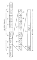
図10に示すように、ディスク製造装置50は、プリ情報生成器51、ビット変換器52、NRZI変換器53、発振器54、移相器55、スイッチ56、レーザ発生器57、対物レンズ58、ディスク載置部62、スピンドルモータ63、送りユニット64、位置検出器65、送りサーボ回路66、回転検出器67および回転サーボ回路68を有する。レーザ発生器57は、レーザ生成部57Aおよび偏向部57Bを備えている。ディスク載置部62上には、スタンパディスク60が載置されている。スタンパディスク60は、レジスト60Aおよびガラス基板60Bを備えている。
【0066】
ディスク製造装置50は、記録プリ情報33に基づいてキャリア信号Sg1を位相変調することによってウォブル信号Sg2を生成し、このウォブル信号Sg2に対応したウォブルを有するグルーブトラック5およびランドトラック7をレジスト60上に形成する。
【0067】
さらに詳しく説明すると、発振器54はキャリア信号Sg1を出力する。キャリア信号Sg1は、2つの経路を通過してスイッチ56の2つの入力端子にそれぞれ供給される。一方の経路を通過したキャリア信号Sg1は、発振器54からスイッチ56に直接供給される。他方の経路を通過したキャリア信号Sg1は、移相器55を介してスイッチ56に供給される。移相器55は、キャリア信号Sg1の移相を180度遅らせまたは進ませる機能を有する。従って、スイッチ56には、キャリア信号Sg1と、キャリア信号Sg1の位相を反転させた信号がそれぞれ同時に供給される。
【0068】
一方、プリ情報生成器51は、プリ情報21を出力する。プリ情報21は、ビット変換器52によって変換プリ情報31に変換され、続いて、NRZI変換器53によって記録プリ情報33に変換され(図7参照)、スイッチ56の制御端子に供給される。
【0069】
スイッチ56は、記録プリ情報33のビットが「0」のとき、キャリア信号Sg1の位相を反転させた信号の通過を許可し、記録プリ情報33のビットが「1」のとき、キャリア信号Sg1の通過を許可する。これにより、記録プリ情報33のビット状態に応じて位相が反転するウォブル信号Sg2が生成される(図8および図9参照)。
【0070】
ウォブル信号Sg2は、スイッチ56からレーザ発生器57の偏向部57Bに供給される。偏向部57Bは、レーザ生成部57Aによって生成されたレーザビームの光軸をウォブル信号Sg2に基づいて微小に傾ける。この結果、レーザ発生器57から対物レンズ58を介してスタンパディスク60のレジスト60Aに照射されるレーザビームのスポット位置は、ウォブル信号Sg2に基づいて半径方向に変調される。
【0071】
このとき、スタンパディスク60は、スピンドルモータ63によって回転している。スタンパディスク60の回転数は、回転検出器67および回転サーボ68によって、所定の速度となるように制御される。さらに、レーザビームの照射時に、スタンパディスク60は、その半径方向に所定の速度で移動する。この移動は、位置検出器65および送りサーボ66によって制御される。
【0072】
このような動作を一体的に行うことにより、スタンパディスク60上に、ウォブルを有する螺旋状または同心円状のグルーブトラック5およびランドトラック7が形成される。そして、光ディスク1の製造の際には、スタンパディスク60が光ディスク1の型として用いられる。
III.記録再生装置
次に、記録再生装置について説明する。図11は、本発明の実施形態による記録再生装置70を示している。記録再生装置70は、記録データを光ディスク1上に記録する機能と、光ディスク1に記録された記録データを再生する機能を備えている。
【0073】
図11に示すように、記録再生装置70は、スピンドルモータ71、ピックアップ73、増幅器75、デコーダ77、信号検出器79、プリアドレスデコーダ81、CPU83、サーボ回路85、エンコーダ87およびレーザ駆動回路89を有している。
【0074】
記録データを光ディスク1に記録するとき、記録再生装置70は、光ディスク1に形成されたウォブル6から、プリ情報21等を読み取る。そして、記録再生装置70は、これら読み取った情報に基づいて、光ディスク1の回転速度を制御し、光ディスク1上の位置を特定しながら、記録データの光ディスク1への記録を行う。
【0075】
このような記録動作についてさらに詳しく説明する。まず、スピンドルモータ71は光ディスク1を所定の初期回転速度で回転させる。ピックアップ73は、回転している光ディスク1に読取用の光ビームを照射し、その反射光を受光し、受光された反射光に対応する読取信号Sg3を出力する。この読取信号Sg3には、ウォブル6を表すウォブル信号成分が含まれている。なお、読取用の光ビームとは、記録用の光ビームに比してその強度が弱くかつ当該強度が一定の光ビームである。
【0076】
読取信号Sg3は、ピックアップ73から増幅器75に供給され、増幅器75により増幅された後、信号検出器79に供給される。信号検出器79は、読取信号Sg3からウォブル信号成分を検出し、これをウォブル検出信号Sg4としてプリアドレスデコーダ81に出力する。このウォブル検出信号Sg4は、上述したウォブル信号Sg2(図10)と実質的に等しい信号であり、プリ情報21を含んでいる。
【0077】
プリアドレスデコーダ81は、ウォブル検出信号Sg4に同期した記録クロックCLの生成、ウォブル検出信号Sg4に基づくプリ情報21の復調、および、ウォブル検出信号Sg4によって決定される所定の周期で初期化・計数を繰り返すカウント値の生成を行う。
【0078】
記録クロックCLは、エンコーダ87に供給され、エンコーダ87による記録データの変調処理において記録データの1ビットの時間間隔を決定するのに用いられる。復調されたプリ情報21は、復調信号Sg5としてCPU83に供給され、CPU83において光ディスク1上の位置の特定に用いられる。カウンタ値は、カウンタ信号Sg6としてCPU83およびサーボ回路85に供給される。カウンタ信号は、CPU83においては、光ディスク1上の位置の特定に用いられ、サーボ回路85においては、光ディスク1の回転を制御するための情報として用いられる。
【0079】
サーボ回路85は、カウンタ信号Sg6等に基づいて、スピンドルモータ71の駆動制御等を行う。
【0080】
記録クロックCLおよびカウンタ値の生成、プリ情報21の復調および光ディスク1の回転制御等が行われている間、CPU83は、外部から記録データを受け取り、これを記録データRDとしてエンコーダ87に供給する。
【0081】
エンコーダ87は、記録データRDに8/16変調およびNRZI変換等を施す。このとき、記録データRDにおける1ビットの時間間隔は、プリアドレスデコーダ81から供給される記録クロックCLによって決定される。エンコーダ87から出力された記録データRDは、レーザ駆動回路89によって光ビームを制御するための制御信号Sg7に変換され、ピックアップ73に供給される。
【0082】
これと同時に、CPU83は、復調信号Sg5およびカウンタ信号Sg6によって記録データRDを記録すべき光ディスク1上の位置を特定する。このとき、CPU83は、復調信号Sg5からプリ情報21をデコードし、プリ情報21からプリアドレスを抽出する。そして、CPU83は、このプリアドレスに基づいて、ECCブロック単位で光ディスク1上の位置を特定する。さらに、CPU83は、デコードしたプリ情報21からセクタ番号データ25を抽出し、これに基づいてセクタ単位で光ディスク1上の位置を特定する。さらに、CPU83は、復調信号Sg5から記録プリ情報33を取得し、この記録プリ情報33のビット数をカウントすることにより、シンクフレーム15単位で光ディスク1上の位置を特定する。
【0083】
記録データRDを記録すべき光ディスク1上の位置を特定した後、CPU83は、その位置から記録データRDが記録されるように、ピックアップ73を光ディスク1の半径方向に移動させ、位置決めする。なお、ピックアップ73の移動制御については、従来のDVD記録装置とほぼ同様である。
【0084】
そして、ピックアップ73は、記録データRDに対応して強度が変化する光ビーム(記録用の光ビーム)を光ディスク1上の特定された位置に向けて出力する。これにより、記録データRDは、光ディスク1のグルーブトラック5上にピット列として記録される。
【0085】
一方、光ディスク1に既に記録された記録データを再生するとき、記録再生装置70は、以下のように動作する。ピックアップ73は、回転している光ディスク1に読取用の光ビームを照射し、その反射光を受光し、受光した反射光に対応する読取信号Sg3を出力する。この読取信号Sg3には、ウォブル信号成分と、光ディスク1に記録された記録データを表す成分が含まれている。
【0086】
読取信号Sg3は、増幅器75により増幅された後、デコーダ77に供給される。デコーダ77は、読取信号Sg3から記録データを表す成分のみを抽出し、これに対して復調処理を行う。さらに、デコーダ77は、復調された記録データを再生データPDとしてCPU83に供給する。そして、再生データPDは、CPU83から外部に出力される。
【0087】
なお、再生動作時においても、記録動作時とほぼ同様に、ウォブル信号成分に基づく記録クロックCLおよびカウント値の生成、および、プリ情報21の復調が行われる。そして、光ディスク1の回転速度の制御等は、プリアドレスデコーダ81から供給されるカウンタ信号Sg6に基づいて、サーボ回路85によって行われる。なお、光ディスク1の回転速度を制御するための情報等は、光ディスク1から読み取られた記録データからも検出することができる。従って、デコーダ77によって、光ディスク1の回転速度を制御するための情報を含む回転制御信号Sg9を生成し、これをサーボ回路85に供給することによって光ディスク1の回転制御を行う構成としてもよい。
【0088】
次に、プリアドレスデコーダ81についてさらに詳しく説明する。プリアドレスデコーダ81では、ウォブル検出信号Sg4に同期した記録クロックCLを生成すると共に、ウォブル検出信号Sg4の位相が非反転状態か反転状態かを検出して復調信号Sg5を生成する。これを実現するために、本発明の実施形態では、PSK(Phase Shift Keying)復調技術として一般に知られているコスタスルーブ法が用いられている。
【0089】
ここで、コスタスルーブ法を用いたPSK復調について図12を用いて説明する。図12は、コスタスルーブ法を用いたPSK復調を実現するための基本回路を示している。図12に示すように、この基本回路110は、PLL回路116により生成されるキャリア信号Sg12と、それに直交する(90度位相がずれた)キャリア信号Sg13により入力信号Sg11を同期検波(乗算)する構成である。
【0090】
以下、この基本回路110の動作を説明する。まず、この基本回路110に、以下の数式1に示すような入力信号Sg11が入力され、この入力信号Sg11に対してキャリア信号Sg12の位相がφだけずれていると仮定する。
【0091】
【数1】

PLL回路116から出力されるキャリア信号Sg12は、2つに分岐し、その一方は乗算器111に直接供給され、他方は、移相器117によってその位相が90度ずらされた後、キャリア信号Sg13として乗算器112に供給される。この結果、乗算器111からは以下の数式2に示すような乗算信号Sg14が得られる。
【0093】
【数2】
また、乗算器112からは以下の数式3に示すような乗算信号Sg15が得られる。
【0095】
【数3】
これら乗算信号Sg14およびSg15は、ローパスフィルタ(LPF)113および114にそれぞれ入力される。そして、ローパスフィルタ113および114によって、上記数式2および3における2wctの成分が乗算信号Sg14およびSg15からそれぞれ除去される。さらに、ローパスフィルタ113および114からの各出力信号Sg16およびSg17は乗算器115によって互いに乗算される。この結果、以下の数式4に示すような位相エラー信号Sg18が得られる。
【0097】
【数4】
この位相エラー信号Sg18は、入力信号Sg11の位相の非反転、反転に拘わらず、位相ずれφが正(キャリア信号Sg12の位相が進んでいる)のときに負の値となり、位相ずれφがゼロのときにはゼロとなり、位相ずれφが負(キャリア信号Sg12の位相が遅れている)ときには正の値となる。
【0099】
PLL回路116は、この位相エラー信号Sg18に基づいて、キャリア信号Sg12の位相が入力信号Sg11に一致するように、キャリア信号Sg12の位相を制御する。
【0100】
さらに、位相ずれφがゼロに制御されているとき、数式2に示す乗算信号Sg14をローパスフィルタ113に入力することによって得られる出力信号Sg16は、入力信号Sg11の位相が非反転状態(sin(ωt))のときに正の値となり、入力信号Sg11の位相が反転状態(−sin(ωt))のときに正の値となる。従って、出力信号Sg16の値が正か負かを識別することにより、入力信号Sg11の位相が非反転状態か反転状態かを認識することができる。
【0101】
さて、図13は、本発明の実施形態によるプリアドレスデコーダ81の内部構造を示している。図13に示すように、PSK復調回路120と位相反転検出回路130とから構成されている。
【0102】
図14は、PSK復調回路120の内部構造を示している。図14に示すように、本発明の実施形態によるPSK復調回路120は、上述した基本回路110の構成をその一部に取り入れた回路である。PSK復調回路120は、3個の乗算器121、122および125、2個のローパスフィルタ123および124、PLL回路126、フレームカウンタ127、カウンタ値デコーダ128および識別回路129を備えている。
【0103】
乗算器121、122、125およびローパスフィルタ123および124は、上述した基本回路110の乗算器111、112、115およびローパスフィルタ113、114とほぼ同様の構成を有する。
【0104】
PLL回路126は、記録クロックCLを生成する回路であり、記録クロックCLの位相がウォブル検出信号Sg4(入力信号)の位相と一致するように、記録クロックCLの位相を位相エラー信号Sg28の値に基づいて制御する回路である。
【0105】
フレームカウンタ127は、PLL回路126から供給される記録クロックCLのクロックを計数し、そのカウント値を出力する回路である。また、フレームカウンタ127は、位相反転検出回路130から供給されるリセット信号Sg35がハイレベルになったときに、カウント値をゼロに初期化する。
【0106】
カウンタ値デコーダ128は、フレームカウンタ127から出力されるカウンタ値に基づいて、ウォブル検出信号Sg4の同期検波に用いるためのパルス信号Sg21と、このパルス信号Sg21に対し位相が90度ずれたパルス信号Sg22を生成する回路である。
【0107】
識別回路129は、ローパスフィルタ123からの出力信号Sg26に基づいてプリ情報21を復調する回路である。
【0108】
図15は、PSK復調回路120の動作を示している。以下、図14および図15を用いてPSK復調回路120の動作を説明する。
【0109】
信号検出器79からプリアドレスデコーダ81にウォブル検出信号Sg4が入力されると(図11参照)、このウォブル検出信号Sg4は、PSK復調回路120に入力される。このとき、PLL回路126は、記録データにおける1ビットの時間間隔に対応したクロック周期を有する記録クロックCLをフレームカウンタ127に出力している。
【0110】
フレームカウンタ127は、この記録クロックCLを計数する。フレームカウンタ127には、位相反転検出回路130からリセット信号Sg35が供給されている。リセット信号Sg35は、図15に示すように、記録クロックCLのクロック数が1488に達する毎にハイレベルとなる。即ち、リセット信号Sg35がハイレベルとなる間隔は、シンクフレーム15の長さ(ウォブル6の最小位相反転周期D1)に一致している。従って、フレームカウンタ127は、記録クロックCLのクロック数が1488に達する毎に、カウンタ値をゼロに初期化しながら、記録クロックCLの計数を繰り返す。図15に示す三角形状の波形は、カウンタ値の初期化・計数が繰り返されている状態を示している。ここで、カウンタ値は、記録クロックCLのクロックパルスを計数しているため、カウンタ値が1増加する周期は、記録クロックCLのクロック周期に等しい。
【0111】
フレームカウンタ127のカウンタ値は、カウンタ値デコーダ128に供給される。カウンタ値デコーダ128は、ウォブル検出信号Sg4の同期検波に用いるためのパルス信号Sg21およびSg22を生成する。
【0112】
図15に示すように、パルス信号Sg21は、その周期がウォブル検出信号Sg4の周期と等しい。そして、記録クロックCLとウォブル検出信号Sg4との間に位相ずれがないと仮定した場合、パルス信号Sg21の位相は、ウォブル検出信号Sgの位相と一致する。本実施形態では、上述したように、ウォブル6の周期が、記録クロックCLの124クロック分の時間間隔に対応する長さに設定されており、シンクフレーム15の長さ、即ち、ウォブル6の最小位相反転間隔D1(図8および図9参照)が記録クロックCLの1488クロック分の時間間隔(1488T)に相当する。従って、シンクフレーム15の長さの1/12がウォブル周期に等しい。これは、ウォブル周期がシンクフレームの長さの約数(1/M:Mは2以上の整数)であることを意味する。このように、ウォブル周期がシンクフレームの長さの約数である場合、シンクフレームの長さに相当するクロック数を単純にMで割るだけでウォブル周期を得ることができる。これにより、カウンタ値デコーダ128は、カウンタ値の変化に基づいて、周波数および位相がウォブル検出信号Sg4の周波数および位相に等しいパルス信号Sg21を容易に生成することができる。
【0113】
さらに、図15に示すように、パルス信号Sg22は、パルス信号Sg21と同一の周波数を有し、パルス信号Sg21に対して位相が90度(1/4周期)ずれた信号である。本実施形態では、ウォブル6の周期が、記録クロックCLの124クロック分の時間間隔に対応する長さに設定されており、124は4の倍数である。これは、ウォブル6の周期が記録クロックCLのクロック周期の4P倍(Pは1以上の整数)であることを意味する。このため、カウンタ値デコーダ128は、パルス信号Sg21に対して1/4周期ずれたパルス信号Sg22を容易に生成することができる。
【0114】
パルス信号Sg21およびSg22は、乗算器121および122にそれぞれ出力される。乗算器121は、パルス信号Sg21とウォブル検出信号Sg4とを互いに乗算し、乗算信号Sg23を出力する。一方、乗算器122は、パルス信号Sg22とウォブル検出信号Sg4とを互いに乗算し、乗算信号Sg24を出力する。乗算信号Sg23およびSg24は、図15に示すような波形となる。
【0115】
乗算信号Sg23およびSg24は、ローパスフィルタ123および124をそれぞれ通過した後、互いに乗算され、位相エラー信号Sg28としてPLL回路126に供給される。これにより、PLL回路126において、記録クロックCLの位相が、ウォブル検出信号Sg4(入力信号)の位相と一致するように制御される。
【0116】
さらに、ローパスフィルタ123の出力信号Sg26は、図15に示すような波形となる。図15中のウォブル検出信号Sg4と出力信号Sg26とを比較すると、出力信号Sg26の値が正のとき、ウォブル検出信号Sg4の位相が非反転状態であり、出力信号Sg26の値が負のとき、ウォブル検出信号Sg4の位相が反転状態であることがわかる。この出力信号Sg26は、識別回路129に供給される。この際、Mの値を大きくとる(本実施形態の場合はM=12である)ことにより、簡単な構成のローパスフィルタで2wctの成分を除去することができる。
【0117】
識別回路129は、出力信号Sg26を、所定のレベル(例えばゼロレベル)を有する基準信号Srfと比較し、図15に示すような復調信号Sg5を生成する。復調信号Sg5は、ウォブル検出信号Sg4が非反転状態か反転状態かに応じてその値が変化するパルス信号である。これは、復調信号Sg5がプリ情報21を示す信号であることを意味する。
【0118】
さらに、PLL回路126によって生成された記録クロックCLはエンコーダ87に、識別回路129から出力された復調信号Sg5はCPU83にそれぞれ供給される。さらにまた、フレームカウンタ127から出力されたカウンタ値はカウンタ信号Sg6としてCPU83およびサーボ回路85に供給される。
【0119】
図16は、位相反転検出回路130の内部構造を示している。位相反転検出回路130は、フレームカウンタ127のカウンタ値をリセットするためリセット信号Sg35を生成する回路である。
【0120】
リセット信号Sg35は、図15に示すように、記録クロックCLのクロック数が1488に達する毎にハイレベルとなり、ハイレベルとなる間隔が、シンクフレーム15の長さ(ウォブル6の最小位相反転周期D1)に一致した信号である。位相反転検出回路130は、このリセット信号Sg35がハイレベルになるタイミングを、PSK復調回路120の識別回路129から出力される復調信号Sg5の立ち上がりエッジおよび立ち下がりエッジに基づいて決定する。
【0121】
ここで、グルーブトラック5に形成されたウォブル6は、記録データの読取への影響をなるべく低くするために、その振幅が小さい。例えば、ウォブル6の振幅はトラックピッチの数%である。この結果、ウォブル検出信号Sg4のSN比は低く、復調信号Sg5の立ち上がりエッジおよび立ち下がりエッジのタイミングはノイズの影響を受けて不安定な場合がある。そこで、位相反転検出回路130は、復調信号Sg5の立ち上がりエッジまたは立ち下がりエッジのタイミングを平均化し、この平均化されたタイミングによって、リセット信号Sg35がハイレベルになるタイミングを決定する。これにより、リセット信号Sg35がハイレベルになるタイミングの精度を高めることができる。
【0122】
図16に示すように、位相反転検出回路130は、エッジ検出回路131、カウンタ133、ホールド回路135、ローパスフィルタ(LPF)137および比較回路139を備えている。
【0123】
図17は、位相反転検出回路130の動作を示している。以下、図16および図17を用いて位相反転検出回路130の動作を説明する。
【0124】
PSK復調回路120の識別回路129から出力された復調信号Sg5は、エッジ検出回路131に入力される。エッジ検出回路131は、復調信号Sg5の立ち上がりエッジおよび立ち下がりエッジを検出する。そして、エッジ検出回路131は、復調信号Sg5の立ち上がりエッジまたは立ち下がりエッジが検出されたタイミングで、タイミング検出信号Sg31をホールド回路135に出力する。
【0125】
一方、PSK復調回路120のPLL回路126によって生成された記録クロックCLは、カウンタ133に入力される。カウンタ133は、記録クロックCLのクロック数を計数し、そのカウント値が1488に達したときに初期化され、以後、計数・初期化を繰り返す。カウンタ133のカウンタ値は、カウンタ信号Sg32としてホールド回路135に出力される。
【0126】
ホールド回路135は、タイミング検出信号Sg31が入力されるタイミング、即ち、復調信号Sg5の立ち上がりエッジまたは立ち下がりエッジが検出されるタイミングで、カウンタ133のカウンタ値を記憶し、その値を次のタイミング検出信号Sg31の入力があるまで保持(ホールド)する。ホールド回路135は、このような動作をタイミング検出信号Sg31が入力される毎に繰り返し行う。
【0127】
ホールド回路135に保持されたカウンタ値は、ローパスフィルタ137に出力され、ローパスフィルタ137によって平均化される。
【0128】
そして、比較回路139は、平均化されたカウンタ値(平均信号Sg33)と、カウンタ133から直接受け取ったカウンタ値(カウンタ信号Sg32)とを比較し、両者が一致したタイミングでハイレベルとなるパルス信号を出力する。このパルス信号がリセット信号Sg35としてPSK復調回路120のフレームカウンタ127に供給される。
【0129】
もし、復調信号Sg5の立ち上がりタイミングまたは立ち下がりタイミングがノイズの影響を受けてずれると、タイミング検出信号Sg31の出力タイミング(タイミング検出信号Sg31がハイレベルとなるタイミング)が変化することになる。このため、ホールド回路135によって記憶保持されるカウンタ値が、タイミング検出信号Sg31の出力タイミングの変化に応じてばらつく。しかしながら、カウンタ値はローパスフィルタ137によって平均化されるため、かかるカウンタ値のばらつきは除去される。これにより、リセット信号Sg35がハイレベルになるタイミングを正確に決定することができる。
【0130】
図18は、PSK復調回路の他の実施形態を示している。上述したPSK復調回路120では、単一のフレームカウンタ127を用いる構成としたが、図18に示すPSK復調回路150のように、ウォブル6の周期をカウントするための第1カウンタ151と、1シンクフレーム15内においてウォブル6に対応する波形が振動する回数をカウントする第2カウンタ153を設ける構成としてもよい。なお、1シンクフレーム15内においてウォブル6に対応する波形が振動する回数は、ウォブル周期が124クロック、1シンクフレームの長さが1488クロックの場合、12である。
【0131】
図19は、位相検出回路の他の実施形態を示している。上述した位相反転検出回路130では、復調信号Sg5の立ち上がりタイミングまたは立ち下がりタイミングをローパスフィルタ137を用いて平均化することによってリセット信号Sg35を生成する構成としたが、図19に示す位相検出回路160のように、PLL回路161を用いてリセット信号Sg35を生成する構成としてもよい。
【0132】
位相検出回路160は、復調信号Sg5の立ち上がりタイミングまたは立ち下がりタイミングと、リセット信号Sg35がハイレベルになるタイミングとをPLL回路161によって同期させる構成である。PLL回路161としては、図18に示すように、位相検出回路163、ループフィルタ165および発信回路167を備えた典型的な構成のPLL回路を用いることができる。そして、PLL回路161の制御帯域を、例えば、100Hz〜1kHz程度とすることにより、復調信号Sg5の立ち上がりタイミングまたは立ち下がりタイミングがノイズの影響を受けてずれても、これに追従しない安定したリセット信号Sg35を生成することが可能となる。
【0133】
図20は、位相検出回路160の動作を示している。図20に示すように、エッジ検出器131は、復調信号Sg5の立ち上がりタイミングおよび立ち下がりタイミングを検出し、各タイミングを示すタイミング検出信号Sg41をPLL回路161に出力する。これにより、発振回路167からは、当該タイミング検出信号Sg41に同期した発振パルス信号Sg42が得られる。この発振パルス信号Sg42の立ち上がりタイミングを、リセット信号Sg35がハイレベルとなるタイミングとして用いることができる。
【0134】
以上より、本発明の実施形態による記録再生装置70によれば、ウォブル6の位相の反転を検出することにより、プリ情報21を復調することができ、プリ情報に基づいて、光ディスク1上の位置を容易かつ正確に特定することができる。
【0135】
また、プリ情報21を復調して復調信号Sg5を生成するとき、シンクフレーム15の長さ(ウォブル6の最小位相反転間隔D1)に同期して初期化・計数を繰り返すカウンタ値(カウンタ信号Sg6)を生成する構成としたから、このカウンタ値を用いて光ディスク1上の位置を高精度に特定することができる。
【0136】
さらに、カウンタ値(カウンタ信号Sg6)を初期化するタイミング、即ち、リセット信号Sg35をハイレベルにするタイミングを決定するとき、復調信号Sg5の立ち上がりタイミングまたは立ち下がりタイミングを平均化する構成としたから、カウンタ値(カウンタ信号Sg6)を初期化するタイミングを正確に決定することができる。従って、カウンタ値(カウンタ信号Sg6)によって光ディスク1上の位置を正確に特定することができる。
【0137】
さらに、PSK復調回路120(150)に、コスタスルーブ法を応用したことにより、ウォブル検出信号Sg4を容易かつ正確に同期検波することができる。このことも、光ディスク1の位置の特定精度の向上に貢献する。
【0138】
このように、本発明の実施形態による記録再生装置70は、光ディスク1の位置を容易かつ正確に特定でき、既に記録データが記録された光ディスク1に新たな記録データを追加して記録するとき、従来のCD−RまたはCD−RWのように、ダミーデータ等を用いてバッファ領域を確保しなくても、既記録データに新記録データが上書きされるのを防止することができる。従って、光ディスク1上の記憶領域の無駄な使用を排除でき、光ディスク1の記憶容量を実質的に増加させることができる。
かかる効果に加え、本発明の実施形態による光ディスク1によれば、再生専用の光ディスクと記録可能な光ディスクとの間で互換性を容易に図ることができる。これにより、再生専用の光ディスクか記録可能な光ディスクかの違いを考慮せずに、光ディスクに記録された情報の再生を共通の記録再生装置70で実現することができる。このことは、当該記録再生装置70の構造の簡単化、コスト低減に貢献する。
【0139】
なお、上述したPSK復調回路120(150)では、ウォブル検出信号Sg4の同期検波に乗算器121および122を用いる場合を例に挙げたが、本発明はこれに限らず、乗算器121および122を、それぞれ、極性反転回路に置き換えてもよい。これにより、PSK復調回路120(150)の構成を簡単化することができる。
【図面の簡単な説明】
【図1】本発明の実施形態による光ディスクを示す図である。
【図2】図1に示す光ディスク上に形成されたトラックを示す拡大図である。
【図3】本発明の実施形態による記録データの構造を示す図である。
【図4】本発明の実施形態によるプリ情報の構造を示す図である。
【図5】本発明の実施形態によるプリ情報の具体的な内容を示す図である。
【図6】本発明の実施形態においてプリ情報のビットを変換するための規則を記述したテーブルを示す図である。
【図7】本発明の実施形態においてプリ情報の変換を示す図である。
【図8】本発明の実施形態において記録プリ情報、キャリア信号およびウォブル信号を示す図である。
【図9】本発明の実施形態においてセクタ、シンクフレーム、記録プリ情報およびウォブルのそれぞれの対応関係を示す図である。
【図10】本発明の実施形態によるディスク製造装置を示すブロック図である。
【図11】本発明の実施形態による情報記録装置を示すブロック図である。
【図12】PSK復調を実現する基本回路を示すブロック図である。
【図13】本発明の実施形態によるプリアドレスデコーダを示すブロック図である。
【図14】本発明の実施形態によるPSK復調回路を示すブロック図である。
【図15】図14に示すPSK復調回路の動作を表す信号波形を示す波形図である。
【図16】本発明の実施形態による位相検出回路を示すブロック図である。
【図17】図16に示す位相検出回路の動作を表す信号波形を示す波形図である。
【図18】本発明の他の実施形態によるPSK復調回路を示すブロック図である。
【図19】本発明の他の実施形態による位相検出回路を示すブロック図である。
【図20】図19に示す位相検出回路の動作を表す信号波形を示す波形図である。
【符号の説明】
1 光ディスク(情報記録ディスク)
3 ディスク面
5 グルーブトラック(トラック)
6 ウォブル
11 セクタ
13 ECCブロック
15 シンクフレーム
17 記録データ(記録情報)
19 シンクパターン(同期信号)
21 プリ情報
33 記録プリ情報(位置情報)
70 記録再生装置(情報記録装置)
73 ピックアップ
79 信号検出器(ウォブル検出手段)
81 プリアドレスデコーダ
83 CPU(位置情報復調手段、記録手段)
120 PSK復調回路(位相検出手段)
130 位相検出反転回路(信号生成手段)[0001]
BACKGROUND OF THE INVENTION
The present invention relates to an information recording disk such as an optical disk used for recording information, and more particularly to an information recording disk having a recording track on which wobbling is formed and capable of additionally recording and rewriting information. Furthermore, the present invention relates to an information recording apparatus for recording information on such an information recording disk.
[0002]
[Prior art]
A CD (Compact Disk) capable of recording information only once is generally known as a CD-R (CD-Recordable). Further, a CD that can rewrite information many times is generally known as a CD-RW (CD-ReWritable). These CD-R and CD-RW recording tracks meander slightly in the radial direction. This meandering of the recording track is generally called wobbling.
[0003]
On the other hand, in order to record information on the disc or to reproduce information recorded on the disc, information indicating an absolute address (or absolute time) on the disc is required. Hereinafter, this information is referred to as pre-information.
[0004]
In CD-R and CD-RW, pre-information is recorded on a disk by FM-modulating wobble. Specifically, the carrier signal used for wobble formation is FM-modulated with pre-information, and a wobble corresponding to the waveform of this FM-modulated carrier signal is formed on the recording track. Thereby, pre-information is recorded on the disc.
[0005]
[Problems to be solved by the invention]
By the way, when information is recorded on a CD-R or CD-RW, or when information recorded on a CD-R or CD-RW is reproduced, the recording device or the reproduction device is recorded on the CD-R or CD-RW. The formed wobble is read, and the rotational speed control of the CD-R or CD-RW and the generation of the recording clock are performed based on the information obtained from the wobble. For this reason, it is not preferable that the wobble frequency changes greatly. Therefore, only a small amount is allowed to change the wobble frequency to superimpose the pre-information on the wobble. For example, when the wobble frequency is 22.05 kHz, the amount by which the wobble frequency is changed in order to superimpose the pre-information is only ± 1 kHz. As a result, it is not easy to accurately detect the pre-information from the wobble by the recording device or the reproducing device, and there is a problem that the accuracy of specifying the position on the disk is low.
[0006]
If the accuracy of specifying the position on the disc is low, the recording position is likely to be shifted when new recording information is added (linked) to the recording information already recorded on the disc. As a result, for example, new recorded information may be overwritten on the already recorded information, or an unpredictable gap may be generated between the already recorded information and the new recorded information. In order to avoid such a situation, in CD-R and CD-RW, a buffer area is secured by recording dummy data following this recording information at the end of writing of the recording information. However, this buffer area has the disadvantage of causing a loss of storage capacity of the disk.
[0007]
On the other hand, in a recordable DVD such as a DVD-RAM, pre-information is recorded on a disc using a method different from CD-R and CD-RW. That is, a recordable DVD employs a method of recording pre-information on a disk by forming pre-pits (embossed pits) on the disk.
[0008]
However, in this method, the difference in structure between a read-only disc and a recordable disc becomes large due to the configuration in which prepits are provided only on a recordable DVD. For this reason, it is difficult to achieve compatibility between the two. For example, there is a problem that it is difficult to perform reproduction of information recorded on a recordable disc having prepits and reproduction of information recorded on a reproduction-only disc having no prepits by a common reproduction means. is there.
[0009]
The present invention has been made in view of such problems, and an object of the present invention is to facilitate compatibility between a read-only recording disk and a recordable recording disk, and on the disk. It is an object of the present invention to provide an information recording disk capable of easily and accurately detecting a recording position of recorded information. Another object of the present invention is to provide an information recording apparatus capable of easily and accurately detecting the recording position of recorded information on a disc.
[0010]
[Means for Solving the Problems]
In order to solve the above-mentioned problem, the invention described in claim 1A track for recording recording information to be reproduced provided on the disc surface, and a wobble provided on the track whose phase changes at a plurality of locations, and a plurality of position information indicating positions on the disc surface. An information recording disc recorded as a group of the same phase of the wobble, wherein the recording information is arranged at a predetermined arrangement cycle and includes a synchronization signal for synchronization when recording or reproducing the recording information When the recording information is recorded on the track, the interval between the group of start positions on the track is N times the synchronization signal arrangement period (N is an integer of 1 or more). An information recording apparatus for recording the recording information on a recording disk, wherein wobble detection means detects a wobble signal corresponding to the wobble from the information recording disk. Detecting the phase of the wobble signal comprises a phase detector for generating a detection signal indicating a change in the phase of the wobble signal, and a position information demodulating means for demodulating said positional information based on the detection signal.
[0011]
In order to solve the above-mentioned problem, the invention according to
[0023]
DETAILED DESCRIPTION OF THE INVENTION
Hereinafter, embodiments of the present invention will be described with reference to the accompanying drawings.
I. optical disk
First, the optical disk will be described. FIG. 1 shows an
[0024]
As shown in FIG. 1, a
[0025]
The
[0026]
The
[0027]
In the conventional DVD-RAM, prepits are formed on the disk surface, but no prepits are formed on the
[0028]
FIG. 2 shows the
[0029]
The
[0030]
The
[0031]
On the other hand, the recording data is not recorded at the manufacturing stage of the
[0032]
Next, the structure of the recording data will be described. FIG. 3 shows the structure (recording format) of the recording data. The
[0033]
More specifically, each
[0034]
The
[0035]
Next, recording of recording data on the
[0036]
The
[0037]
The recording data (
[0038]
Next, the structure of pre-information will be described. FIG. 4 shows the structure of the
[0039]
The
[0040]
The
[0041]
The pre-data 27 is data indicating any one of a pre-address on the
[0042]
As shown in FIG. 5, the
[0043]
In FIG. 5, the pre-information 21 corresponding to the
[0044]
Next, recording of the pre-information 21 on the
[0045]
After the
[0046]
The first purpose of the bit conversion is to make it possible to easily identify the
[0047]
The second purpose of the bit conversion is to limit the bit inversion interval of the
[0048]
The NRZI conversion is performed for the purpose of reducing noise such as a DC component generated in a signal corresponding to the pre-information 21 in the process of recording the pre-information 21 (recorded pre-information 33) as the
[0049]
The
[0050]
FIG. 8 shows a correspondence relationship between the
[0051]
The
[0052]
Next, the relationship between the phase inversion interval of the
[0053]
This will be described in more detail. The
[0054]
One bit of the
[0055]
Furthermore, as shown in FIG. 9, on the
[0056]
Next, setting of the cycle of the
[0057]
As described above, according to the
[0058]
Further, the
[0059]
That is, in the conventional recordable DVD-RAM, pre-information is recorded by forming pre-pits. As a result, there is a large structural difference between a recordable DVD and a read-only DVD, and there is a problem that it is difficult to achieve compatibility between both discs. The
[0060]
Thus, the
[0061]
In the
[0062]
Further, in the
[0063]
Furthermore, in the
[0064]
Further, in the
II. Disc manufacturing equipment
Next, the disk manufacturing apparatus will be described. FIG. 10 shows a
[0065]
As shown in FIG. 10, the
[0066]
The
[0067]
More specifically, the
[0068]
On the other hand, the pre information generator 51 outputs the
[0069]
The
[0070]
The wobble signal Sg2 is supplied from the
[0071]
At this time, the
[0072]
By integrally performing such an operation, the spiral or
III. Recording / playback device
Next, the recording / reproducing apparatus will be described. FIG. 11 shows a recording / reproducing
[0073]
As shown in FIG. 11, the recording / reproducing
[0074]
When recording the record data on the
[0075]
Such a recording operation will be described in more detail. First, the
[0076]
The read signal Sg3 is supplied from the
[0077]
The
[0078]
The recording clock CL is supplied to the
[0079]
The
[0080]
While the generation of the recording clock CL and the counter value, the demodulation of the
[0081]
The
[0082]
At the same time, the
[0083]
After specifying the position on the
[0084]
Then, the
[0085]
On the other hand, when reproducing the recorded data already recorded on the
[0086]
The read signal Sg3 is amplified by the
[0087]
Note that, during the reproducing operation, the recording clock CL and the count value based on the wobble signal component are generated, and the
[0088]
Next, the
[0089]
Here, PSK demodulation using the Costa lube method will be described with reference to FIG. FIG. 12 shows a basic circuit for realizing PSK demodulation using the Costa lube method. As shown in FIG. 12, the
[0090]
Hereinafter, the operation of the
[0091]
[Expression 1]
The carrier signal Sg12 output from the
[0093]
[Expression 2]
Further, the
[0095]
[Equation 3]
These multiplication signals Sg14 and Sg15 are input to low-pass filters (LPF) 113 and 114, respectively. Then, the low-
[0097]
[Expression 4]
This phase error signal Sg18 takes a negative value when the phase shift φ is positive (the phase of the carrier signal Sg12 is advanced) regardless of whether the phase of the input signal Sg11 is non-inverted or inverted, and the phase shift φ is zero. Is zero, and is positive when the phase shift φ is negative (the phase of the carrier signal Sg12 is delayed).
[0099]
Based on the phase error signal Sg18, the
[0100]
Furthermore, when the phase shift φ is controlled to zero, the output signal Sg16 obtained by inputting the multiplication signal Sg14 shown in
[0101]
FIG. 13 shows the internal structure of the
[0102]
FIG. 14 shows the internal structure of the
[0103]
The
[0104]
The
[0105]
The
[0106]
The
[0107]
The
[0108]
FIG. 15 shows the operation of the
[0109]
When the wobble detection signal Sg4 is input from the
[0110]
The
[0111]
The counter value of the
[0112]
As shown in FIG. 15, the period of the pulse signal Sg21 is equal to the period of the wobble detection signal Sg4. When it is assumed that there is no phase shift between the recording clock CL and the wobble detection signal Sg4, the phase of the pulse signal Sg21 matches the phase of the wobble detection signal Sg. In the present embodiment, as described above, the period of the
[0113]
Furthermore, as shown in FIG. 15, the pulse signal Sg22 is a signal having the same frequency as the pulse signal Sg21 and having a phase shifted by 90 degrees (1/4 cycle) from the pulse signal Sg21. In the present embodiment, the period of the
[0114]
Pulse signals Sg21 and Sg22 are output to
[0115]
Multiplication signals Sg23 and Sg24 pass through low-
[0116]
Further, the output signal Sg26 of the low-
[0117]
The
[0118]
Further, the recording clock CL generated by the
[0119]
FIG. 16 shows the internal structure of the phase
[0120]
As shown in FIG. 15, the reset signal Sg35 becomes a high level every time the number of clocks of the recording clock CL reaches 1488, and the interval of the high level is the length of the sync frame 15 (the minimum phase inversion period D1 of the wobble 6). ). The phase
[0121]
Here, the amplitude of the
[0122]
As shown in FIG. 16, the phase
[0123]
FIG. 17 shows the operation of the phase
[0124]
The demodulated signal Sg5 output from the
[0125]
On the other hand, the recording clock CL generated by the
[0126]
The
[0127]
The counter value held in the
[0128]
Then, the
[0129]
If the rising timing or falling timing of the demodulated signal Sg5 is shifted due to the influence of noise, the output timing of the timing detection signal Sg31 (the timing at which the timing detection signal Sg31 becomes high level) changes. For this reason, the counter value stored and held by the
[0130]
FIG. 18 shows another embodiment of the PSK demodulation circuit. The
[0131]
FIG. 19 shows another embodiment of the phase detection circuit. In the phase
[0132]
The
[0133]
FIG. 20 shows the operation of the
[0134]
As described above, according to the recording / reproducing
[0135]
Further, when demodulating signal Sg5 is generated by demodulating
[0136]
Further, when determining the timing for initializing the counter value (counter signal Sg6), that is, the timing for setting the reset signal Sg35 to the high level, the rising timing or falling timing of the demodulated signal Sg5 is averaged. The timing for initializing the counter value (counter signal Sg6) can be accurately determined. Therefore, the position on the
[0137]
Furthermore, by applying the Costa lube method to the PSK demodulating circuit 120 (150), the wobble detection signal Sg4 can be detected synchronously easily and accurately. This also contributes to the improvement of the position specifying accuracy of the
[0138]
As described above, the recording / reproducing
In addition to this effect, the
[0139]
In the above-described PSK demodulating circuit 120 (150), the case where the
[Brief description of the drawings]
FIG. 1 is a diagram showing an optical disc according to an embodiment of the present invention.
FIG. 2 is an enlarged view showing a track formed on the optical disc shown in FIG.
FIG. 3 is a diagram showing a structure of recording data according to an embodiment of the present invention.
FIG. 4 is a diagram illustrating a structure of pre-information according to an embodiment of the present invention.
FIG. 5 is a diagram illustrating specific contents of pre-information according to an embodiment of the present invention.
FIG. 6 is a diagram showing a table describing rules for converting bits of pre-information in the embodiment of the present invention.
FIG. 7 is a diagram illustrating conversion of pre-information in the embodiment of the present invention.
FIG. 8 is a diagram showing recording pre-information, a carrier signal, and a wobble signal in the embodiment of the present invention.
FIG. 9 is a diagram illustrating a correspondence relationship between sectors, sync frames, recording pre-information, and wobbles in the embodiment of the present invention.
FIG. 10 is a block diagram showing a disk manufacturing apparatus according to an embodiment of the present invention.
FIG. 11 is a block diagram showing an information recording apparatus according to an embodiment of the present invention.
FIG. 12 is a block diagram showing a basic circuit for realizing PSK demodulation.
FIG. 13 is a block diagram illustrating a pre-address decoder according to an embodiment of the present invention.
FIG. 14 is a block diagram illustrating a PSK demodulation circuit according to an embodiment of the present invention.
15 is a waveform diagram showing signal waveforms representing the operation of the PSK demodulator circuit shown in FIG. 14;
FIG. 16 is a block diagram showing a phase detection circuit according to an embodiment of the present invention.
17 is a waveform diagram showing signal waveforms representing the operation of the phase detection circuit shown in FIG. 16;
FIG. 18 is a block diagram showing a PSK demodulation circuit according to another embodiment of the present invention.
FIG. 19 is a block diagram showing a phase detection circuit according to another embodiment of the present invention.
20 is a waveform diagram showing signal waveforms representing the operation of the phase detection circuit shown in FIG. 19;
[Explanation of symbols]
1 Optical disc (information recording disc)
3 Disc surface
5 Groove track (track)
6 Wobble
11 sectors
13 ECC block
15 Sync frame
17 Recording data (recording information)
19 Sync pattern (synchronization signal)
21 Pre-information
33 Recording pre-information (position information)
70 Recording / playback device (information recording device)
73 Pickup
79 Signal detector (wobble detection means)
81 Pre-address decoder
83 CPU (Position information demodulating means, recording means)
120 PSK demodulation circuit (phase detection means)
130 Phase detection inversion circuit (signal generation means)
Claims (6)
前記ウォブルに対応したウォブル信号を前記情報記録ディスクから検出するウォブル検出手段と、
前記ウォブル信号の位相を検出し、前記ウォブル信号の位相の変化を示す検出信号を生成する位相検出手段と、
前記検出信号に基づいて前記位置情報を復調する位置情報復調手段と、
を備えたことを特徴とする情報記録装置。A track for recording recording information to be reproduced provided on the disc surface, and a wobble provided on the track whose phase changes at a plurality of locations, and a plurality of position information indicating positions on the disc surface. An information recording disk recorded as a group of the same phase of the wobble, wherein the recording information is arranged at a predetermined arrangement cycle and includes a synchronization signal for synchronization when recording or reproducing the recording information When the recording information is recorded on the track, the interval between the group of start positions on the track is N times the synchronization signal arrangement period (N is an integer of 1 or more). An information recording apparatus for recording the recording information on a recording disk,
Wobble detection means for detecting a wobble signal corresponding to the wobble from the information recording disk;
Phase detection means for detecting a phase of the wobble signal and generating a detection signal indicating a change in the phase of the wobble signal;
Position information demodulating means for demodulating the position information based on the detection signal;
An information recording apparatus comprising:
前記位置情報復調手段により復調された位置情報と前記信号生成手段により生成された制御信号に基づいて前記ディスク面上の記録位置を特定し、前記一群の開始位置の間隔が前記同期信号の配置周期のN倍(Nは1以上の整数)となるように、前記記録情報を前記特定された記録位置から記録する記録手段と、
を更に備えたことを特徴とする請求項1に記載の情報記録装置。Signal generating means for detecting the timing of the start position of the group from the detection signal and generating a control signal indicating the arrangement period of the synchronization signal in the recording information based on the timing;
The recording position on the disk surface is specified based on the position information demodulated by the position information demodulating means and the control signal generated by the signal generating means, and the interval between the group of start positions is the arrangement period of the synchronization signals. Recording means for recording the recording information from the specified recording position so as to be N times N (N is an integer of 1 or more);
The information recording apparatus according to claim 1, further comprising:
前記ウォブルに対応したウォブル信号を前記情報記録ディスクから検出するウォブル検出工程と、
前記ウォブル信号の位相を検出し、前記ウォブル信号の位相の変化を示す検出信号を生成する位相検出工程と、
前記検出信号に基づいて前記位置情報を復調する位置情報復調工程と、
前記ウォブル信号の同位相の一群の開始位置の間隔が、前記記録情報における同期信号の配置周期のN倍(Nは1以上の整数)に相当するように、前記記録情報を前記情報記録ディスクに記録する記録工程と、
を含むことを特徴とする情報記録方法。 A track for recording provided et Re recorded information to be reproduced disk surface, and a wobble phase changes at a plurality of locations provided in the track, the position information indicating the position on the disk surface An information recording method for recording the recording information on an information recording disk recorded as a group of the same phase of a plurality of wobbles,
A wobble detection step of detecting a wobble signal corresponding to the wobble from the information recording disc ;
Detecting a phase of the wobble signal and generating a detection signal indicating a change in the phase of the wobble signal; and
A position information demodulation step of demodulating the position information based on the detection signal ;
The recording information is recorded on the information recording disc so that the interval between the start positions of a group of the same phase of the wobble signal corresponds to N times (N is an integer of 1 or more) the arrangement period of the synchronization signal in the recording information. A recording process for recording;
Information recording how, which comprises a.
Priority Applications (4)
| Application Number | Priority Date | Filing Date | Title |
|---|---|---|---|
| JP29381499A JP3850600B2 (en) | 1999-10-15 | 1999-10-15 | Information recording disk and information recording apparatus |
| US09/689,825 US6434091B1 (en) | 1999-10-15 | 2000-10-13 | Information record disc and information recording apparatus |
| EP00309039A EP1093123B1 (en) | 1999-10-15 | 2000-10-13 | Information record disc |
| US10/196,250 US6587428B2 (en) | 1999-10-15 | 2002-07-17 | Information record disc and information recording apparatus |
Applications Claiming Priority (1)
| Application Number | Priority Date | Filing Date | Title |
|---|---|---|---|
| JP29381499A JP3850600B2 (en) | 1999-10-15 | 1999-10-15 | Information recording disk and information recording apparatus |
Related Child Applications (1)
| Application Number | Title | Priority Date | Filing Date |
|---|---|---|---|
| JP2005097099A Division JP2005196968A (en) | 2005-03-30 | 2005-03-30 | Information recording disk and information recording disk reproducing device |
Publications (3)
| Publication Number | Publication Date |
|---|---|
| JP2001118255A JP2001118255A (en) | 2001-04-27 |
| JP2001118255A5 JP2001118255A5 (en) | 2005-09-15 |
| JP3850600B2 true JP3850600B2 (en) | 2006-11-29 |
Family
ID=17799504
Family Applications (1)
| Application Number | Title | Priority Date | Filing Date |
|---|---|---|---|
| JP29381499A Expired - Lifetime JP3850600B2 (en) | 1999-10-15 | 1999-10-15 | Information recording disk and information recording apparatus |
Country Status (3)
| Country | Link |
|---|---|
| US (2) | US6434091B1 (en) |
| EP (1) | EP1093123B1 (en) |
| JP (1) | JP3850600B2 (en) |
Families Citing this family (23)
| Publication number | Priority date | Publication date | Assignee | Title |
|---|---|---|---|---|
| CN1193350C (en) * | 1999-11-03 | 2005-03-16 | 三星电子株式会社 | Identification data addressing method, swinging address coding circuit and detecting method and circuit |
| TWI235363B (en) * | 2001-03-16 | 2005-07-01 | Koninkl Philips Electronics Nv | Record carrier and apparatus for scanning the record carrier |
| JP4874472B2 (en) * | 2001-06-08 | 2012-02-15 | 三星電子株式会社 | Optical disk drive and driving method switching method thereof |
| JP3559540B2 (en) * | 2001-09-07 | 2004-09-02 | 株式会社東芝 | Multipurpose information storage medium, storage method, reproduction method and reproduction apparatus |
| CN1220981C (en) * | 2001-10-15 | 2005-09-28 | 日本胜利株式会社 | Information recording carrier |
| NZ532275A (en) * | 2001-10-15 | 2005-08-26 | Konink Philips Electronics N | Record carrier and apparatus for scanning the record carrier |
| JP4121265B2 (en) | 2001-10-16 | 2008-07-23 | コーニンクレッカ フィリップス エレクトロニクス エヌ ヴィ | Disc-shaped recording medium, disc drive apparatus, disc manufacturing apparatus and method |
| JP4121264B2 (en) | 2001-10-16 | 2008-07-23 | コーニンクレッカ フィリップス エレクトロニクス エヌ ヴィ | Disk drive device and wobble information detection method |
| KR100811628B1 (en) * | 2001-11-06 | 2008-03-11 | 엘지전자 주식회사 | Writable optical disc recorded wobble address and, apparatus and method for detecting the wobble address thereof |
| KR100946226B1 (en) * | 2001-12-21 | 2010-03-09 | 코닌클리케 필립스 일렉트로닉스 엔.브이. | Record carrier and scanning device |
| JP2003203347A (en) | 2001-12-28 | 2003-07-18 | Toshiba Corp | Information storage medium, information recording device, information reproducing device, information recording method, and information reproducing method |
| JP2003203357A (en) * | 2001-12-28 | 2003-07-18 | Toshiba Corp | Information storage medium, information recorder, information reproducing device, information recording method and information reproducing method |
| JP3561259B2 (en) | 2002-01-09 | 2004-09-02 | 株式会社東芝 | Information storage medium, information recording device, information reproducing device, information recording method, and information reproducing method |
| JP4115173B2 (en) * | 2002-06-11 | 2008-07-09 | ソニー株式会社 | Disc recording medium, disc manufacturing method, disc drive apparatus |
| KR100677106B1 (en) * | 2002-12-10 | 2007-02-01 | 삼성전자주식회사 | Information storage medium and method for recording/reproducing the same |
| TWI289836B (en) * | 2003-01-23 | 2007-11-11 | Toshiba Corp | Information recording medium, information recording/reproducing method, and information recording/reproducing device |
| EP1585131A1 (en) * | 2004-04-06 | 2005-10-12 | Deutsche Thomson-Brandt Gmbh | Circuit for wobble demodulation |
| JP2006155849A (en) * | 2004-11-04 | 2006-06-15 | Canon Inc | Reproducing apparatus |
| JP4142656B2 (en) * | 2005-02-23 | 2008-09-03 | 富士通株式会社 | Optical disk WAP demodulation method and demodulator |
| US7586831B2 (en) * | 2005-03-21 | 2009-09-08 | Alliance Storage Technologies, Inc. | Amplitude modulated addressing in disk pregroove |
| US11234608B2 (en) | 2011-09-02 | 2022-02-01 | Battelle Memorial Institute | Extravasation and infiltration detection device with fluid guide provided on a substrate of the detection device to adjust fluid rate based on detection signal |
| US9875220B2 (en) * | 2012-11-09 | 2018-01-23 | The Boeing Company | Panoptic visualization document printing |
| US9680526B2 (en) * | 2014-12-26 | 2017-06-13 | Panasonic Intellectual Property Management Co., Ltd. | Phase error detector and optical disc device |
Family Cites Families (9)
| Publication number | Priority date | Publication date | Assignee | Title |
|---|---|---|---|---|
| KR900000464B1 (en) * | 1984-10-05 | 1990-01-30 | 가부시기가이샤 히다찌세이사꾸쇼 | A demodulation circuit |
| JP3344495B2 (en) * | 1993-03-04 | 2002-11-11 | ソニー株式会社 | Magnetic disk drive |
| JP2849033B2 (en) * | 1993-11-11 | 1999-01-20 | パイオニア株式会社 | optical disk |
| US5878007A (en) * | 1993-12-27 | 1999-03-02 | Matsushita Electric Industrial Co., Ltd. | Anti-wobble optical medium and tracking method and apparatus |
| JPH1069646A (en) | 1996-08-29 | 1998-03-10 | Ricoh Co Ltd | Optical disk medium, optical disk device |
| CN1516131A (en) * | 1996-10-22 | 2004-07-28 | ������������ʽ���� | Information recording medium and playback device capable of expressing magnetic track swinging information |
| CN1136554C (en) * | 1996-10-25 | 2004-01-28 | 松下电器产业株式会社 | Optical disc having oscillating lands and grooves |
| JPH10320781A (en) * | 1997-05-20 | 1998-12-04 | Pioneer Electron Corp | Prepit signal detector and detection |
| US6192015B1 (en) * | 1997-11-06 | 2001-02-20 | Lg Electronics Inc. | Method and apparatus for recording and reproducing recording medium |
-
1999
- 1999-10-15 JP JP29381499A patent/JP3850600B2/en not_active Expired - Lifetime
-
2000
- 2000-10-13 EP EP00309039A patent/EP1093123B1/en not_active Expired - Lifetime
- 2000-10-13 US US09/689,825 patent/US6434091B1/en not_active Expired - Fee Related
-
2002
- 2002-07-17 US US10/196,250 patent/US6587428B2/en not_active Expired - Lifetime
Also Published As
| Publication number | Publication date |
|---|---|
| US20020191508A1 (en) | 2002-12-19 |
| JP2001118255A (en) | 2001-04-27 |
| US6587428B2 (en) | 2003-07-01 |
| EP1093123B1 (en) | 2012-06-13 |
| EP1093123A1 (en) | 2001-04-18 |
| US6434091B1 (en) | 2002-08-13 |
Similar Documents
| Publication | Publication Date | Title |
|---|---|---|
| JP3850600B2 (en) | Information recording disk and information recording apparatus | |
| JP3845849B2 (en) | Recording apparatus, recording method, and recording medium | |
| JP3703569B2 (en) | Optical recording medium, recording / reproducing method thereof, and recording / reproducing apparatus | |
| JP3555055B2 (en) | Prepit detection device and information recording device | |
| JP3843560B2 (en) | Asymmetry correction device and asymmetry correction method | |
| JP4355459B2 (en) | Information recording / reproducing apparatus and pre-pit detecting method | |
| US6980494B1 (en) | Optical disc recording method and apparatus, optical disc, and optical disc reproducing apparatus | |
| JP3845951B2 (en) | Disc-shaped recording medium, disc reproducing apparatus, and disc reproducing method | |
| JP3881835B2 (en) | Recording / playback device | |
| JP2001357627A (en) | Information recording method and its device | |
| JP3961338B2 (en) | Optical disk device | |
| JPH11306685A (en) | Signal processing circuit | |
| JPH09120584A (en) | Optical disk, optical disk recording and reproducing device and method, and optical disk forming device and method | |
| JP4557272B2 (en) | Recording / reproducing apparatus and method | |
| EP1548735A1 (en) | Optical disk recorder, method of recording information, and information recording medium | |
| JP3714117B2 (en) | Pre-pit detection device, pre-pit detection method, position and frequency signal detection circuit | |
| JPH11306686A (en) | Signal processing circuit | |
| JPH0719431B2 (en) | Optical disc recording / reproducing device | |
| JP2005196968A (en) | Information recording disk and information recording disk reproducing device | |
| JPH10154332A (en) | Movement control information recording device, recording medium recorded with movement control information and information recording device | |
| JP3888067B2 (en) | Clock generation circuit and recording / reproducing apparatus using the same | |
| JP3627237B2 (en) | Optical disc and optical disc recording apparatus | |
| JP4130785B2 (en) | Recording device | |
| JP3836448B2 (en) | Recording and / or playback device | |
| JP3739764B2 (en) | Optical recording medium |
Legal Events
| Date | Code | Title | Description |
|---|---|---|---|
| A521 | Request for written amendment filed |
Free format text: JAPANESE INTERMEDIATE CODE: A523 Effective date: 20050330 |
|
| A621 | Written request for application examination |
Free format text: JAPANESE INTERMEDIATE CODE: A621 Effective date: 20050330 |
|
| A871 | Explanation of circumstances concerning accelerated examination |
Free format text: JAPANESE INTERMEDIATE CODE: A871 Effective date: 20050330 |
|
| A975 | Report on accelerated examination |
Free format text: JAPANESE INTERMEDIATE CODE: A971005 Effective date: 20050629 |
|
| A131 | Notification of reasons for refusal |
Free format text: JAPANESE INTERMEDIATE CODE: A131 Effective date: 20050705 |
|
| A521 | Request for written amendment filed |
Free format text: JAPANESE INTERMEDIATE CODE: A523 Effective date: 20050831 |
|
| A131 | Notification of reasons for refusal |
Free format text: JAPANESE INTERMEDIATE CODE: A131 Effective date: 20060620 |
|
| A521 | Request for written amendment filed |
Free format text: JAPANESE INTERMEDIATE CODE: A523 Effective date: 20060807 |
|
| TRDD | Decision of grant or rejection written | ||
| A01 | Written decision to grant a patent or to grant a registration (utility model) |
Free format text: JAPANESE INTERMEDIATE CODE: A01 Effective date: 20060829 |
|
| A61 | First payment of annual fees (during grant procedure) |
Free format text: JAPANESE INTERMEDIATE CODE: A61 Effective date: 20060830 |
|
| R150 | Certificate of patent or registration of utility model |
Free format text: JAPANESE INTERMEDIATE CODE: R150 Ref document number: 3850600 Country of ref document: JP Free format text: JAPANESE INTERMEDIATE CODE: R150 |
|
| FPAY | Renewal fee payment (event date is renewal date of database) |
Free format text: PAYMENT UNTIL: 20100908 Year of fee payment: 4 |
|
| FPAY | Renewal fee payment (event date is renewal date of database) |
Free format text: PAYMENT UNTIL: 20100908 Year of fee payment: 4 |
|
| FPAY | Renewal fee payment (event date is renewal date of database) |
Free format text: PAYMENT UNTIL: 20110908 Year of fee payment: 5 |
|
| FPAY | Renewal fee payment (event date is renewal date of database) |
Free format text: PAYMENT UNTIL: 20120908 Year of fee payment: 6 |
|
| FPAY | Renewal fee payment (event date is renewal date of database) |
Free format text: PAYMENT UNTIL: 20120908 Year of fee payment: 6 |
|
| FPAY | Renewal fee payment (event date is renewal date of database) |
Free format text: PAYMENT UNTIL: 20130908 Year of fee payment: 7 |
|
| EXPY | Cancellation because of completion of term |