JP3965553B2 - TAB tape manufacturing method - Google Patents
TAB tape manufacturing method Download PDFInfo
- Publication number
- JP3965553B2 JP3965553B2 JP2002016683A JP2002016683A JP3965553B2 JP 3965553 B2 JP3965553 B2 JP 3965553B2 JP 2002016683 A JP2002016683 A JP 2002016683A JP 2002016683 A JP2002016683 A JP 2002016683A JP 3965553 B2 JP3965553 B2 JP 3965553B2
- Authority
- JP
- Japan
- Prior art keywords
- substrate
- copper foil
- hole
- tab tape
- sprocket
- Prior art date
- Legal status (The legal status is an assumption and is not a legal conclusion. Google has not performed a legal analysis and makes no representation as to the accuracy of the status listed.)
- Expired - Fee Related
Links
Images


Landscapes
- Wire Bonding (AREA)
Description
【0001】
【発明の属する技術分野】
本発明は、半導体素子をプリント配線板上に実装するための半導体パッケージの部材として用いられるTABテープの製造方法に関する。
【0002】
【従来の技術】
パソコンやOA機器、家電製品、音響機器、ゲーム機などに代表される電子機器においては半導体素子を直接プリント配線板上に実装することが難しい。そのため、半導体素子はインターポーザーと呼ばれる基板に搭載された半導体パッケージという形態にしてから、電子機器装置に実装することが多くなっている。
【0003】
実装作業において、プリント配線板上に半導体パッケージを搭載する自動実装機へのパーツ供給を効率良く行わねばならない。そのため、テープ状(長尺帯状)のインターポーザー基板上に半導体素子を載せて、電気的な導電配線を施し、半導体素子周辺を樹脂封止することでテープ状のインターポーザー基板上に所定の間隔を持って、連続した半導体パッケージが作られる。これが一般に、TAB(Tape Automated Bonding)と呼称される。
【0004】
テープ状のインターポーザー基板の基板となるフイルム基板は、35mm、48mm、70mm幅が標準的なサイズといえる。フイルム基板の表面に銅めっきを施した後、レジスト塗布、レジストへのパターン露光、現像、エッチング、レジスト剥離といったフォトエッチング処理を行い、フイルム基板上に配線層を形成したインターポーザー基板となる。通常フイルム基板の幅方向の両端に四角い穴が所定の間隔で設けられている。前記四角い穴をスプロケットホールと呼び、自動実装機の搬送系ではスプロケットホールに歯車の歯をひっかけるなどしてインターポーザー基板の搬送を行っている。また、自動実装機の搬送系は映画の映写機などの技術を応用したものなので、スプロケットホールに関する寸法規格は映画などのフィルムの端についている四角形の穴と同じ規格で作られている。
【0005】
図5(a)に示すように、このスプロケットホールは、従来、インターポーザー基板を製造する工程の最初に金型でフイルム基板を打ち抜いて形成していた。
【0006】
近年、量産性を考慮して100mm以上の広幅のフイルム基板を使い、一度に、幅方向に複数個の半導体素子を搭載できるよう、多条取りレイアウトでTABを製造することが多くなってきている。
【0007】
【発明が解決しようとする課題】
図5(a)は、多条取りレイアウトとした時のフイルム基板の事例を示す。なを、図5の破線部は半導体素子が搭載される領域を示す。図に示すように、多条取りレイアウトにおいては、フイルム基板の端部に加えて、内部領域にもスプロケットホールを形成する必要がある。しかし、多条取りレイアウトにおいて従来どおり、工程の初期段階で必要なスプロケットホールを形成してしまうと、テープの幅方向の端部だけではなく基材の内部まで貫通穴が開いてしまう。そのため、液状の配線パターン形成用レジスト樹脂のコーティングの際、液状レジスト材が裏抜けしてしまったり、フイルム基板の片面だけに行う銅めっき工程において、コーティングでは裏抜けしてしまったり、又は、薬液がスプロケットホールを通じて、裏抜けしない様にマスキングする手間が増えてしまうといった問題点があった。
【0008】
又、従来技術において、この前記問題点を解決する方法として、工程の初期段階に広幅の基材の幅方向の端部のスプロケットホール列のみ設けておき、配線パターンの形成および絶縁性樹脂層の形成した後で、基板の内部領域スプロケットホールを金型にて打ち抜く方法がある。
【0009】
しかし、この方法の場合、同じ工程を2度行うため、打ち抜き装置の処理能力が半減するばかりでなく、打ち抜き前のTABテープは製品としては、ほぼ完成品となっているので、この工程で打ち抜き位置を間違えてしまうと、収量、収率に影響を及ぼすリスクの大きい作業となる。
【0010】
本発明の課題は、多条取りレイアウトとしたTABテープの製造方法において、基板の内部領域に形成したスプロケットホール貫通穴によって、レジスト樹脂のコーティング工程時に、コーティング液の裏抜けする問題と、TABテープの片面だけに行う銅めっき工程時、裏面に薬液が裏抜けしない様に、内部領域に形成したスプロケットホールをマスキングする手間が増える問題点を解消することにある。又、2度手間の打ち抜きによる収率が低下する問題点を解消することにある。
【0011】
【課題を解決するための手段】
以上の課題を解決するための本願の請求項1に記載の発明は、絶縁性樹脂の両面に銅箔が積層されてなる基板の両端部に基板搬送用の第1のスプロケットホールを穿設した後、基板の他の領域に実装時の搬送に使用する第2のスプロケットホールを穿設するTABテープの製造方法であって、第2のスプロケットホールをTABテープの加工時の銅箔エッチング工程と同時に穿設することを特徴とするTABテープの製造方法である。
請求項2に記載の発明は、TABテープの製造方法において、前記第2スプロケットホール穿設工程が、
(a)前記TABテープの両面のうち片側の面の銅箔及び絶縁性樹脂に外堀状の溝状の穴を設ける工程と、
(b)前記TABテープの両面のうち前記外堀状の溝状の穴を設けた面の反対の面からエッチングをして、基板部分のうち外堀状の溝状の穴に囲まれた部分を脱落させる工程と、を含んでなることを特徴とする請求項1に記載のTABテープの製造方法である。
請求項3に記載の発明は、絶縁性樹脂の両面に銅箔が積層されてなる基板の両端部に基板搬送用の第1のスプロケットホールを穿設した後、基板の他の領域に実装時の搬送に使用する第2スプロケットホールを穿設するTABテープの製造方法であって、
(a)第1のスプロケットホールを穿設する工程と、
(b)第2のスプロケットホールを形成するため、基板の両面に形成した銅箔のうち、片面の銅箔にフォトエッチング法にて作ったメタルマスクに炭酸ガスレーザーを照射する工程と、を含んでなることを特徴とする請求項1に記載のTABテープの製造方法である。
【0014】
【作用】
多条取りレイアウトのTABテープの製造方法において、TABテープの製造工程の最初の段階で必要なスプロケットホールを一度に形成する従来の方法から、TABテープの搬送用に必要なスプロケットホールを工程の最初の段階でテープの幅方向の端部のみ形成し、基板の内部領域に形成する、半導体素子の実装時に使用するスプロケットホールは、銅箔のエッチング工程と同時に開ける分割形成の方法に変更する。
【0015】
【発明の実施の形態】
以下、本発明の実施の形態を図を用いて説明する。
【0016】
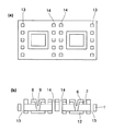
図1に示す本発明のTABテープの平面図と側断面図である。まず長尺帯状の基板の両端部に形成するスプロケットホール13は、従来通り金型にて打抜く方法で形成した。該基板両端に形成する第1のスプロケットホール13はTABテープを製造する工程で使用する基板の搬送用ものである。次に、基板の内部領域には、半導体素子実装時に使用する第2のスプロケットホール14を形成している。スプロケットホール14の形成は、基板の両面に形成した銅箔のうち、片面の銅箔にフォトエッチング法にて、スプロケットホールをエッチングして作るメタルマスクに炭酸ガスレーザーを照射する方法や、又は、UV‐YAGレーザー加工機等にて、片側の銅箔とポリイミドとも同時に打ち抜く加工方法を使い、内部領域スプロケットホールの外周形状とした外堀状の溝状の穴を穿設する。外堀状の溝状の穴の囲まれた基板部位は他方の銅箔のみで保持される。すなわち、前記他方の銅箔のみで保持された基板部位は、他方の銅箔をエッチングする工程の終了後に脱落する。すなわち、前記外堀状の溝状の穴と、他方の銅箔のエッチング部とにより、貫通したスプロケットホールが形成される。
【0017】
なお、最近では、片側に銅箔を接着した基材に適度な接着性のある銅箔複合材を張り合わせた両面銅箔付の基材を使い、片面配線TABを作ることもある。しかし、この本発明の技術は両面銅付基材から作られる両面配線TABテープのみに限定されるものではなく、片面配線TABテープにも適用可能な技術である。
【0018】
図2図3は本発明の製造工程を説明する工程図を示した物であり、図2(a)〜(e)及び図3(f)〜(h)は各工程の側断面図である。
【0019】
図2(a)は、両面銅箔付ポリイミド基板の断面を示す。
【0020】
図2(b)は、打ち抜き金型で打ち抜きを行い両面銅箔付ポリイミド基板の端部に第1のスプロケットホール13を形成した断面を示す。
【0021】
次いで、UV‐YAGレーザー加工機等を用いて、内部領域のスプロケットホールの外形を形成する外堀状の溝状の穴4、及び表裏面の銅箔間を電気的に接続するための導通用非貫通孔5に対応した片面の銅箔にのみ穴を穿孔しており、他方の銅箔端そのままとしている。すなわち、穴4,5は他方の銅箔12を残した非貫通の穴としている。図2(c)参照する。
【0022】
次いで図2(d)は、穴4,5に形成面側から銅めっきを行う。銅めっきのより導通用非貫通孔5穴内全面に銅めっきが付くことで、表裏面の銅箔間が電気的に接続される。
【0023】
図2(e)は、片方の銅箔側に配線パターンを形成するために所定の開口部を有するエッチング用レジストをパターン7を形成した。他方の銅箔12の全面に保護用(エッチング防止のため)レジスト(保護用感光性レジスト8)を形成した。
【0024】
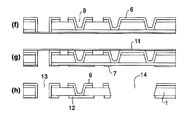
図3(f)は、塩化鉄液などをエッチング液として、銅箔をエッチングした後、レジストを剥膜を行う。これにより銅箔2側に所定の配線パターンが形成される。なお、他方の銅箔12側は、保護されているため、エッチングされずに残る。
【0025】
図3(g)は、銅箔12側に所定の配線パターンを形成するために、所定の開口部を有するエッチング用レジストパターン7を形成する。なお、銅箔2側には保護用に全面塗布した感光性レジスト11を形成している。又、内部領域の第2のスプロケットホールを形成する領域のレジストパターン7部位は、当該スプロケットホールと略同一の開口部を形成している。
【0026】
図3(h)は、他方の銅箔12側にエッチングを行った後、レジスト7,11を剥膜する。本考案の方法で作成したスプロケットホールの断面を示す。端部スプロケットホール13と、内部領域に第2のスプロケットホール14を有するTABテープが得られる。
【0027】
ここで、銅箔12がエッチングされた際、内部領域スプロケットホール14を形成すべき部位に残された基板部位は、支えとなる銅箔12がエッチングされなくなる、そのためエッチング時、若しくは剥膜時に前記の残された基板部位は脱落して、最終的に内部領域スプロケットホール14が得られる。又、スプロケットホールの穴内全面に付着した銅めっきも同時にエッチング除去される。
【0028】
【実施例】
本発明のTABテープの製造方法の一事例を図4に示す工程図(a)〜(d)によって説明する。なお、図4は本発明を示す工程図の平面図と、該側断面図を並列して記している。
【0029】
<実施例1>
図4(a)の基板は105mm幅であり、50μm厚のポリイミド1、その両面に各々厚み12μmの銅箔を表銅箔2と、裏銅箔12を接着したテープ状基板を作製した。
【0030】
次に、このテープ状の基板の端部に、幅方向の中心線から左右に46.52mm離れた位置を中心とする1.98mm角の穴を2個1組としてテープ状基板の長手方向に4.75mmずつの間隔で第1スプロケットホール3を金型を用いて、打ち抜き加工した。
【0031】
次に、図4(b)は、内部領域に第2スプロケットホールの外形となる外堀状の溝状の非貫通穴列4と、表裏間の導通用ビア用の非貫通穴5のパターンをUV‐YAGレーザー加工機にて形成した。なお、加工の際、他方の銅箔12には貫通しないようにレーザー加工したもので、穴4,5は他方の銅箔12により非貫通となっている。
【0032】
UV‐YAGレーザーによる加工はレーザーをスポット状にしたものを決められた位置に照射し、加工を行うもので、加工を始める際に基準となる点が必要である。本実施例においては、レーザーで加工する非貫通穴の位置をある1つのスプロケットホールの重心位置を基準とした。加工は、所定のピッチにて、同じ作業を繰り返し行った。又加工位置の決め方について説明すると、最初に指定したスプロケットホールから光学的に重心位置に算出し、レーザー加工を行い、次に長尺方向に4個先のスプロケットホールについて重心位置を算出し、新たな基準とする様にして、連続的に加工を行った。
【0033】
レーザー加工機で作成する非貫通穴は、直径60μmの非貫通穴とし、レーザーは銅箔2側の表面より照射した。
【0034】
なお、本実施例では、レーザー加工の基準として、スプロケットホールの重心位置を用いたが、別方法として、スプロケットホールを形成する際に直径100から500μmのスプロケットホールより小さい貫通穴をスプロケットホールの外周部の近傍に作成し、これをレーザー加工を行うスプロケットホールの基準とする方法もある。
【0035】
次いで、得られた非貫通穴に銅めっきすることで、表裏銅箔間の導通とる導通ビア9が作られる。本実施例では、銅めっきを行う前に、レーザー加工で付着したススなどを除去するために過マンガン酸カリウムの水溶液で基板表面の洗浄処理を行なった。次に、絶縁材料であるポリイミドにも電気銅めっきが付くように無電解銅めっき処理を行った。この際、スプロケットホール用のレーザー加工穴にめっきが入ってしまうが、銅めっきされてしまっても問題ない。この点に付いては後述する。なお、電気銅めっきを行う前に、銅箔2側にのみ銅が析出される様に、裏面の銅箔12側は液状のレジスト材を全面に塗布して保護してから行った。
【0036】
図4(c)は、上記銅めっき後、銅箔2および12を所定の配線パターンに形成するが、本実施例では、銅箔2側、銅箔12側の順に別々にパターン形成を行った。手順は配線を形成する側の銅箔に液状の感光性レジストをロールコーターで塗布し、配線パターンを露光した後、感光性レジストを現像して、銅箔エッチング用のマスクを作成した。その際、エッチング装置内に脱落する個片状のポリイミド部位が回収できる様であれば、この部分のレジストによる保護は不要であるが、こうした機構がない場合、貫通していないスプロケットホールの部分は感光性レジストによって、エッチングされないように保護する必要がある。なお、反対側の銅箔がエッチングされないように液状の感光性レジストを全面塗布した感光性レジスト8を形成し保護した。
【0037】
次に、表の銅箔2をエッチング処理し、感光性レジストを剥膜した。次に、裏面の銅箔12側の配線形成も銅箔2側と同様にして行った。すなわち、銅箔2側全面に保護用レジストを形成し、銅箔12側に配線パターン用の開口部を有するレジストパターンした後、エッチングを行ったものである。この際、穴4で囲まれた内部領域スプロケットホール部位面の他方の銅箔12がエッチングが入る様に、当該部位には感光性レジストが無いように開口部状態とした。
【0038】
他方の銅箔12側のエッチング処理を行うと、前記銅箔12側に所定の配線パターンが形成されると同時に内部領域スプロケットホール部位面の銅箔もエッチングされ銅箔12による保持を失う。しかし、保護用レジストで保持されている。しかる後、感光性レジストを剥離すると、保護用レジストで保持されていた前記部位が(貫通していなかったスプロケットホールの部分が)脱落する。貫通穴の状態となり、貫通している基板内部のスプロケットホール14が得られる。
【0039】
【発明の効果】
従来はパターニング用の感光性レジストの塗工をディップコートにより行っていたが、本発明によりロールコーターで感光性レジストが塗工できる様になり、より狭い配線パターンをつくることができる様になった。製造工程でマスキングの手間が省け、製造効率が向上する。又、二度手間によるパンチングに起因する収率の低下を防止できる。
【図面の簡単な説明】
【図1】 本発明のテープキャリアの一例を示す概略図で、(a)は平面図で、(b)は側断面図である。
【図2】 本発明の製造工程を説明する工程図を示した物であり、(a)〜(e)は各工程の側断面図である。
【図3】 本発明の製造工程を説明する工程図を示した物であり、(f)〜(h)は各工程の側断面図である。
【図4】 本発明の製造工程を説明する工程図を平面図及び側断面図で示した物であり、(a)〜(d)は各工程の平面図及び側断面図である。
【図5】 従来の製造工程を説明する部分工程図を示した物であり(a)は従来の工程の平面図で(b)は本発明の工程の平面図である。
【符号の説明】
1…ポリイミド
2…銅箔
3…貫通している基板端部のスプロケットホール
4…外堀状の溝状の穴
5…導通用非貫通孔
6…銅めっき
7…エッチング用レジストパターン
8…保護用感光性レジスト
9…表裏導通ビア
10…貫通している基板内部のスプロケットホール
11…保護用感光性レジスト
12…銅箔
13…端部スプロケットホール
14…内部領域スプロケットホール
15…TABテープ
16…半導体素子搭載領域[0001]
BACKGROUND OF THE INVENTION
The present invention relates to a method for manufacturing a TAB tape used as a member of a semiconductor package for mounting a semiconductor element on a printed wiring board.
[0002]
[Prior art]
In electronic devices typified by personal computers, OA devices, home appliances, audio devices, game machines, etc., it is difficult to mount semiconductor elements directly on a printed wiring board. For this reason, the semiconductor element is often mounted on an electronic device after it is in the form of a semiconductor package mounted on a substrate called an interposer.
[0003]
In mounting work, parts must be efficiently supplied to an automatic mounting machine that mounts a semiconductor package on a printed wiring board. Therefore, a semiconductor element is placed on a tape-shaped (long band) interposer substrate, electrically conductive wiring is provided, and the periphery of the semiconductor element is resin-sealed to form a predetermined interval on the tape-shaped interposer substrate. With this, a continuous semiconductor package is made. This is generally called TAB (Tape Automated Bonding).
[0004]
A film substrate that is a substrate for a tape-shaped interposer substrate has a standard size of 35 mm, 48 mm, and 70 mm. After the copper plating is applied to the surface of the film substrate, a photoetching process such as resist coating, resist pattern exposure, development, etching, and resist stripping is performed to form an interposer substrate having a wiring layer formed on the film substrate. Usually, square holes are provided at predetermined intervals at both ends in the width direction of the film substrate. The called the square hole of the sprocket holes, the conveying system of an automatic mounting machine is performing the conveyance of the interposer substrate and the like takes either hit the teeth of the gear to the sprocket holes. In addition, since the transport system of the automatic mounting machine is an application of technology such as a movie projector, the dimensional standard for sprocket holes is made in the same standard as the rectangular hole attached to the end of a film such as a movie.
[0005]
As shown in FIG. 5A, this sprocket hole has been conventionally formed by punching a film substrate with a mold at the beginning of the process of manufacturing an interposer substrate.
[0006]
In recent years, taking into account mass productivity, TAB is often manufactured in a multi-strip layout so that a plurality of semiconductor elements can be mounted in the width direction at a time using a wide film substrate of 100 mm or more. .
[0007]
[Problems to be solved by the invention]
FIG. 5A shows an example of a film substrate when a multi-stripe layout is adopted. The broken line portion in FIG. 5 indicates a region where a semiconductor element is mounted. As shown in the figure, in the multi-row layout, it is necessary to form sprocket holes in the inner region in addition to the end portion of the film substrate. However, if the necessary sprocket holes are formed at the initial stage of the process in the multi-strike layout as before, the through holes are opened not only at the ends in the width direction of the tape but also inside the substrate. Therefore, when coating a liquid wiring pattern forming resist resin, the liquid resist material may be broken through, or in the copper plating process performed only on one side of the film substrate, the coating may be broken through, or a chemical solution However, there is a problem that the time and effort for masking through the sprocket hole so as not to get through is increased.
[0008]
In the prior art, as a method for solving this problem, only the sprocket hole row at the end in the width direction of the wide base material is provided in the initial stage of the process, and the formation of the wiring pattern and the insulating resin layer There is a method of punching the inner region sprocket hole of the substrate with a mold after the formation.
[0009]
However, in this method, since the same process is performed twice, not only the processing capacity of the punching device is halved, but the TAB tape before punching is almost finished as a product, so punching in this process If the position is wrong, it can be a risky operation that affects yield and yield.
[0010]
SUMMARY OF THE INVENTION An object of the present invention is to provide a method for manufacturing a TAB tape having a multi-strip layout, and a problem that a coating liquid is exposed through a sprocket hole through-hole formed in an inner region of a substrate during a resist resin coating process. When the copper plating process is performed only on one side of the substrate, it is necessary to eliminate the problem of increasing the effort of masking the sprocket holes formed in the internal region so that the chemical solution does not escape on the back side. Another object of the present invention is to eliminate the problem of a decrease in yield due to twice punching.
[0011]
[Means for Solving the Problems]
In order to solve the above problems, the invention according to
Invention of
(A) a step of providing an outer moat-like groove-like hole in the copper foil and the insulating resin on one side of both sides of the TAB tape;
(B) Etching from the opposite surface of the surface of the TAB tape opposite to the surface provided with the outer moat-shaped groove-shaped hole, and removing the portion surrounded by the outer moat-shaped groove-shaped hole in the substrate portion The method for producing a TAB tape according to
According to the third aspect of the present invention, after mounting the first sprocket hole for transporting the substrate on both ends of the substrate in which the copper foil is laminated on both surfaces of the insulating resin, A TAB tape manufacturing method for drilling a second sprocket hole used for transporting
(A) drilling a first sprocket hole;
(B) irradiating a metal mask made by photoetching on one side of the copper foil formed on both sides of the substrate to form the second sprocket hole with a carbon dioxide laser; The method for producing a TAB tape according to
[0014]
[Action]
In the manufacturing method of TAB tape of multi-strip layout, the sprocket holes necessary for transporting TAB tape are changed from the conventional method in which the necessary sprocket holes are formed at the first stage of the TAB tape manufacturing process at the beginning of the process. At this stage, only the end in the width direction of the tape is formed, and the sprocket hole used for mounting the semiconductor element formed in the inner region of the substrate is changed to a method of split formation that is opened simultaneously with the copper foil etching process.
[0015]
DETAILED DESCRIPTION OF THE INVENTION
Hereinafter, embodiments of the present invention will be described with reference to the drawings.
[0016]
It is the top view and side sectional drawing of the TAB tape of this invention shown in FIG. First, the
[0017]
Recently, a single-sided wiring TAB is sometimes made using a base material with a double-sided copper foil in which a copper foil composite material having an appropriate adhesive property is bonded to a base material having a copper foil bonded to one side. However, the technique of the present invention is not limited to the double-sided wiring TAB tape made of the double-sided copper-attached base material, but can be applied to a single-sided wiring TAB tape.
[0018]
FIG. 2 is a process diagram illustrating the manufacturing process of the present invention, and FIGS. 2 (a) to (e) and FIGS. 3 (f) to (h) are side sectional views of the respective processes. .
[0019]
Fig.2 (a) shows the cross section of a polyimide board with a double-sided copper foil.
[0020]
FIG. 2B shows a cross section in which the
[0021]
Next, using a UV-YAG laser processing machine or the like, a non-conductive layer for electrically connecting the outer moat-shaped groove-shaped
[0022]
Next, in FIG. 2D, copper plating is performed on the
[0023]
In FIG. 2E, a
[0024]
FIG. 3 (f) and iron chloride solution as an etching solution, after the copper foil has been etched, performs剥膜resist. Thereby, a predetermined wiring pattern is formed on the
[0025]
Figure 3 (g), in order to form a predetermined wiring pattern on the
[0026]
In FIG. 3 (h), after etching the
[0027]
Here, when the
[0028]
【Example】
An example of the method for producing the TAB tape of the present invention will be described with reference to process diagrams (a) to (d) shown in FIG. FIG. 4 shows a plan view of the process diagram showing the present invention and a side sectional view in parallel.
[0029]
<Example 1>
The substrate shown in FIG. 4A was 105 mm wide, and a tape-like substrate was prepared by adhering 50 μm-
[0030]
Next, at the end of the tape-shaped substrate, two 1.98 mm square holes centering on a position 46.52 mm away from the center line in the width direction are set in the longitudinal direction of the tape-shaped substrate. The first sprocket holes 3 were punched using a mold at intervals of 4.75 mm.
[0031]
Next, FIG. 4B shows a pattern of the outer trench-shaped groove-like non-through-
[0032]
The processing by the UV-YAG laser is to perform processing by irradiating a laser beam in a spot shape to a predetermined position, and a reference point is required when starting processing. In this embodiment, the position of the non-through hole processed by the laser is based on the position of the center of gravity of one sprocket hole. In the processing, the same operation was repeated at a predetermined pitch. Also, how to determine the machining position will be explained. First, the center of gravity is optically calculated from the specified sprocket hole, laser processing is performed, then the center of gravity is calculated for the four sprocket holes ahead in the longitudinal direction. In this way, continuous processing was performed.
[0033]
The non-through holes created by the laser processing machine were non-through holes with a diameter of 60 μm, and the laser was irradiated from the surface on the
[0034]
In this embodiment, the position of the center of gravity of the sprocket hole is used as a reference for laser processing. Alternatively, when the sprocket hole is formed, a through hole smaller than the sprocket hole having a diameter of 100 to 500 μm is formed on the outer periphery of the sprocket hole. There is also a method in which it is created in the vicinity of a part and used as a reference for a sprocket hole for laser processing.
[0035]
Next, by conducting copper plating on the obtained non-through hole, a conductive via 9 is formed which conducts electricity between the front and back copper foils. In this example, the substrate surface was cleaned with an aqueous solution of potassium permanganate in order to remove soot and the like attached by laser processing before copper plating. Next, the electroless copper plating process was performed so that the copper which is an insulating material was also electroplated. At this time, the laser processing hole for the sprocket hole is plated, but there is no problem even if it is plated with copper. This point will be described later. Before performing the copper electroplating, the
[0036]
In FIG. 4C, after the copper plating, the copper foils 2 and 12 are formed in a predetermined wiring pattern. In this example, the patterns were formed separately in the order of the
[0037]
Next, the
[0038]
When the
[0039]
【The invention's effect】
Conventionally, the photosensitive resist for patterning was applied by dip coating. However, according to the present invention, the photosensitive resist can be applied with a roll coater, and a narrower wiring pattern can be formed. . This eliminates the masking process in the manufacturing process and improves manufacturing efficiency. Moreover, the fall of the yield resulting from punching by 2 times labor can be prevented.
[Brief description of the drawings]
FIG. 1 is a schematic view showing an example of a tape carrier of the present invention, where (a) is a plan view and (b) is a side sectional view.
FIGS. 2A to 2E are process diagrams illustrating the manufacturing process of the present invention, and FIGS. 2A to 2E are side sectional views of the respective processes. FIGS.
FIGS. 3A to 3H are process diagrams illustrating the manufacturing process of the present invention, and FIGS. 3F to 3H are side sectional views of the respective processes. FIGS.
4A and 4B are plan views and side sectional views showing process drawings for explaining the manufacturing process of the present invention, and FIGS. 4A to 4D are plan views and side sectional views of the respective steps.
FIG. 5 is a partial process diagram for explaining a conventional manufacturing process, in which (a) is a plan view of the conventional process and (b) is a plan view of the process of the present invention.
[Explanation of symbols]
DESCRIPTION OF
Claims (3)
(a)前記TABテープの両面のうち片側の面の銅箔及び絶縁性樹脂に外堀状の溝状の穴を設ける工程と、
(b)前記TABテープの両面のうち前記外堀状の溝状の穴を設けた面の反対の面からエッチングをして、基板部分のうち外堀状の溝状の穴に囲まれた部分を脱落させる工程と、
を含んでなることを特徴とする請求項1に記載のTABテープの製造方法。 In the TAB tape manufacturing method, the second sprocket hole drilling step includes:
(A) a step of providing an outer moat-like groove-like hole in the copper foil and the insulating resin on one side of both sides of the TAB tape;
(B) Etching from the opposite surface of the surface of the TAB tape opposite to the surface provided with the outer moat-shaped groove-shaped hole, and removing the portion surrounded by the outer moat-shaped groove-shaped hole in the substrate portion A process of
The method for producing a TAB tape according to claim 1, comprising:
(a)第1のスプロケットホールを穿設する工程と、(A) drilling a first sprocket hole;
(b)第2のスプロケットホールを形成するため、基板の両面に形成した銅箔のうち、片面の銅箔にフォトエッチング法にて作ったメタルマスクを解してレーザー照射する工程と、(B) to form a second sprocket hole, among the copper foils formed on both sides of the substrate, a step of irradiating a laser with a metal mask made by photoetching on one side of the copper foil;
を含んでなることを特徴とする請求項1に記載のTABテープの製造方法。The method for producing a TAB tape according to claim 1, comprising:
Priority Applications (1)
| Application Number | Priority Date | Filing Date | Title |
|---|---|---|---|
| JP2002016683A JP3965553B2 (en) | 2002-01-25 | 2002-01-25 | TAB tape manufacturing method |
Applications Claiming Priority (1)
| Application Number | Priority Date | Filing Date | Title |
|---|---|---|---|
| JP2002016683A JP3965553B2 (en) | 2002-01-25 | 2002-01-25 | TAB tape manufacturing method |
Publications (2)
| Publication Number | Publication Date |
|---|---|
| JP2003218171A JP2003218171A (en) | 2003-07-31 |
| JP3965553B2 true JP3965553B2 (en) | 2007-08-29 |
Family
ID=27652667
Family Applications (1)
| Application Number | Title | Priority Date | Filing Date |
|---|---|---|---|
| JP2002016683A Expired - Fee Related JP3965553B2 (en) | 2002-01-25 | 2002-01-25 | TAB tape manufacturing method |
Country Status (1)
| Country | Link |
|---|---|
| JP (1) | JP3965553B2 (en) |
-
2002
- 2002-01-25 JP JP2002016683A patent/JP3965553B2/en not_active Expired - Fee Related
Also Published As
| Publication number | Publication date |
|---|---|
| JP2003218171A (en) | 2003-07-31 |
Similar Documents
| Publication | Publication Date | Title |
|---|---|---|
| JP2005236244A (en) | Circuit board manufacturing method | |
| JP2011139064A (en) | Circuit board and method for manufacturing the same | |
| JP6819608B2 (en) | Multi-layer printed wiring board and its manufacturing method | |
| JP2004119968A (en) | Fine wire circuit | |
| JP7333210B2 (en) | Method for manufacturing printed wiring board | |
| JPH1051137A (en) | Method for manufacturing printed wiring board | |
| JP2004031710A (en) | Manufacturing method of wiring board | |
| JP5317491B2 (en) | Method for manufacturing printed wiring board | |
| JP3965553B2 (en) | TAB tape manufacturing method | |
| JP4456834B2 (en) | Laser processing method and metal foil with carrier used therefor | |
| TWI429348B (en) | Multi-layer pcb modules with lateral conductive pads and fabrication methods thereof | |
| JP2007173727A (en) | Wiring board manufacturing method | |
| KR100772432B1 (en) | Printed Circuit Board Manufacturing Method | |
| JPH10189805A (en) | Electronic component mounting substrate and method of manufacturing the same | |
| JP2004087697A (en) | Manufacturing method of wiring board | |
| JP2001358257A (en) | Method of manufacturing substrate for semiconductor device | |
| JP4150464B2 (en) | Two-metal tape carrier package and its manufacturing method | |
| JP2005057077A (en) | Wiring board manufacturing method | |
| TWI234423B (en) | Method for making a circuit board | |
| JPH0770834B2 (en) | Printed circuit board with exposed inner layer pattern part, and method of manufacturing the same | |
| JP5235107B2 (en) | Printed wiring board and manufacturing method thereof | |
| JPH1117315A (en) | Manufacture of flexible circuit board | |
| JP2647007B2 (en) | Manufacturing method of printed wiring board | |
| JPH0336319B2 (en) | ||
| JP4252227B2 (en) | Manufacturing method of double-sided flexible circuit board |
Legal Events
| Date | Code | Title | Description |
|---|---|---|---|
| A621 | Written request for application examination |
Free format text: JAPANESE INTERMEDIATE CODE: A621 Effective date: 20041216 |
|
| A977 | Report on retrieval |
Free format text: JAPANESE INTERMEDIATE CODE: A971007 Effective date: 20051110 |
|
| A131 | Notification of reasons for refusal |
Free format text: JAPANESE INTERMEDIATE CODE: A131 Effective date: 20051115 |
|
| A521 | Written amendment |
Free format text: JAPANESE INTERMEDIATE CODE: A523 Effective date: 20060116 |
|
| A131 | Notification of reasons for refusal |
Free format text: JAPANESE INTERMEDIATE CODE: A131 Effective date: 20070206 |
|
| A521 | Written amendment |
Free format text: JAPANESE INTERMEDIATE CODE: A523 Effective date: 20070405 |
|
| TRDD | Decision of grant or rejection written | ||
| A01 | Written decision to grant a patent or to grant a registration (utility model) |
Free format text: JAPANESE INTERMEDIATE CODE: A01 Effective date: 20070502 |
|
| A61 | First payment of annual fees (during grant procedure) |
Free format text: JAPANESE INTERMEDIATE CODE: A61 Effective date: 20070515 |
|
| R150 | Certificate of patent or registration of utility model |
Free format text: JAPANESE INTERMEDIATE CODE: R150 |
|
| FPAY | Renewal fee payment (event date is renewal date of database) |
Free format text: PAYMENT UNTIL: 20100608 Year of fee payment: 3 |
|
| FPAY | Renewal fee payment (event date is renewal date of database) |
Free format text: PAYMENT UNTIL: 20110608 Year of fee payment: 4 |
|
| FPAY | Renewal fee payment (event date is renewal date of database) |
Free format text: PAYMENT UNTIL: 20110608 Year of fee payment: 4 |
|
| FPAY | Renewal fee payment (event date is renewal date of database) |
Free format text: PAYMENT UNTIL: 20120608 Year of fee payment: 5 |
|
| FPAY | Renewal fee payment (event date is renewal date of database) |
Free format text: PAYMENT UNTIL: 20120608 Year of fee payment: 5 |
|
| FPAY | Renewal fee payment (event date is renewal date of database) |
Free format text: PAYMENT UNTIL: 20130608 Year of fee payment: 6 |
|
| LAPS | Cancellation because of no payment of annual fees |