JP3962441B2 - Semiconductor device - Google Patents
Semiconductor device Download PDFInfo
- Publication number
- JP3962441B2 JP3962441B2 JP25176596A JP25176596A JP3962441B2 JP 3962441 B2 JP3962441 B2 JP 3962441B2 JP 25176596 A JP25176596 A JP 25176596A JP 25176596 A JP25176596 A JP 25176596A JP 3962441 B2 JP3962441 B2 JP 3962441B2
- Authority
- JP
- Japan
- Prior art keywords
- wiring
- input
- transistor
- transistors
- output cell
- Prior art date
- Legal status (The legal status is an assumption and is not a legal conclusion. Google has not performed a legal analysis and makes no representation as to the accuracy of the status listed.)
- Expired - Lifetime
Links
Images


Classifications
-
- H—ELECTRICITY
- H01—ELECTRIC ELEMENTS
- H01L—SEMICONDUCTOR DEVICES NOT COVERED BY CLASS H10
- H01L27/00—Devices consisting of a plurality of semiconductor or other solid-state components formed in or on a common substrate
- H01L27/02—Devices consisting of a plurality of semiconductor or other solid-state components formed in or on a common substrate including semiconductor components specially adapted for rectifying, oscillating, amplifying or switching and having at least one potential-jump barrier or surface barrier; including integrated passive circuit elements with at least one potential-jump barrier or surface barrier
- H01L27/04—Devices consisting of a plurality of semiconductor or other solid-state components formed in or on a common substrate including semiconductor components specially adapted for rectifying, oscillating, amplifying or switching and having at least one potential-jump barrier or surface barrier; including integrated passive circuit elements with at least one potential-jump barrier or surface barrier the substrate being a semiconductor body
- H01L27/10—Devices consisting of a plurality of semiconductor or other solid-state components formed in or on a common substrate including semiconductor components specially adapted for rectifying, oscillating, amplifying or switching and having at least one potential-jump barrier or surface barrier; including integrated passive circuit elements with at least one potential-jump barrier or surface barrier the substrate being a semiconductor body including a plurality of individual components in a repetitive configuration
- H01L27/118—Masterslice integrated circuits
-
- H—ELECTRICITY
- H01—ELECTRIC ELEMENTS
- H01L—SEMICONDUCTOR DEVICES NOT COVERED BY CLASS H10
- H01L24/00—Arrangements for connecting or disconnecting semiconductor or solid-state bodies; Methods or apparatus related thereto
- H01L24/01—Means for bonding being attached to, or being formed on, the surface to be connected, e.g. chip-to-package, die-attach, "first-level" interconnects; Manufacturing methods related thereto
- H01L24/02—Bonding areas ; Manufacturing methods related thereto
- H01L24/04—Structure, shape, material or disposition of the bonding areas prior to the connecting process
- H01L24/06—Structure, shape, material or disposition of the bonding areas prior to the connecting process of a plurality of bonding areas
-
- H—ELECTRICITY
- H01—ELECTRIC ELEMENTS
- H01L—SEMICONDUCTOR DEVICES NOT COVERED BY CLASS H10
- H01L2224/00—Indexing scheme for arrangements for connecting or disconnecting semiconductor or solid-state bodies and methods related thereto as covered by H01L24/00
- H01L2224/01—Means for bonding being attached to, or being formed on, the surface to be connected, e.g. chip-to-package, die-attach, "first-level" interconnects; Manufacturing methods related thereto
- H01L2224/02—Bonding areas; Manufacturing methods related thereto
- H01L2224/04—Structure, shape, material or disposition of the bonding areas prior to the connecting process
- H01L2224/05—Structure, shape, material or disposition of the bonding areas prior to the connecting process of an individual bonding area
- H01L2224/0554—External layer
- H01L2224/0555—Shape
- H01L2224/05552—Shape in top view
- H01L2224/05554—Shape in top view being square
Description
【0001】
【発明の属する技術分野】
本発明は半導体装置(IC)に係り、より詳しくは入出力セル領域に関する。
近年の半導体装置は、製造プロセス技術の進歩により高集積化が進み、半導体チップに構成できる回路の増加に応じて外部ピンの増加が要求されている。半導体装置の多ピン化を図るためには、半導体チップの周縁に沿うように配置される入出力用の外部パッドの配置ピッチを短縮することが必要である。これと同時に、外部パッドの内側において半導体チップの周縁に沿うように配置される入出力回路を構成するための入出力セル領域の幅、すなわち、入出力セル領域の配置方向における長さを短縮することが必要である。
【0002】
【従来の技術】
ICの1つの形態としてゲートアレイがある。図8は従来のCMOSゲートアレイの入出力セル領域100を使用して構成された出力回路101を示す。入出力セル領域100は4個のnMOSトランジスタ102及び4個のpMOSトランジスタ103を備えている。MOSトランジスタのゲートがnMOSトランジスタ102及びpMOSトランジスタ103として示されている。
【0003】
4つのnMOSトランジスタ102の3つの電極であるゲート、ソース及びドレインは入出力セル領域100の幅方向、すなわち、複数の入出力セル領域100の配置方向に並ぶように配置され、4個のpMOSトランジスタ103の3つの電極であるゲート、ソース及びドレインも入出力セル領域100の幅方向に並ぶように配置されている。4個のnMOSトランジスタ102及び4個のpMOSトランジスタ103は入出力セル領域100の高さ方向、すなわち、入出力セル領域100の配置方向と直交する方向に配置されており、4個のnMOSトランジスタ102及び4個のpMOSトランジスタ103はそれぞれ対応している。
【0004】
各nMOSトランジスタ102のソース上には入出力セル領域100の配置方向と直交する方向に金属配線層第1層のアルミニウム配線104が設けられている。アルミニウム配線104は、入出力セル領域100の配置方向に延びかつ低電位電源(VSS)を供給するための金属配線層第2層のアルミニウム電源配線106に接続されている。各pMOSトランジスタ103のソース上には入出力セル領域100の配置方向と直交する方向に金属配線層第1層のアルミニウム配線105が設けられている。アルミニウム配線105は入出力セル領域100の配置方向に延びかつ高電位電源(VDD)を供給するための金属配線層第2層のアルミニウム電源配線107に接続されている。それぞれ対応するnMOSトランジスタ102及びpMOSトランジスタ103のドレインは、入出力セル領域100の配置方向と直交する方向に延びる金属配線層第1層のアルミニウム配線108を介して図示しない外部パッドに接続されている。
【0005】
【発明が解決しようとする課題】
ところが、上記の入出力セル領域100では、nMOSトランジスタ102のソースに低電位電源を供給するアルミニウム配線104、pMOSトランジスタ103のソースに高電位電源を供給するアルミニウム配線105、対応するnMOSトランジスタ102及びpMOSトランジスタ103のドレインを外部パッドに接続するためのアルミニウム配線108は、金属配線層第1層に設けられている。そのため、金属配線層第1層は、アルミニウム配線104,105,108や、ゲートコンタクト用の配線で混雑する。
【0006】
また、対応するnMOSトランジスタ102及びpMOSトランジスタ103のドレインを外部パッドに接続するためのアルミニウム配線108はソース上のアルミニウム配線に接触しないように避けて設ける必要があるとともに、エレクトロマイグレーション耐性を向上するためにアルミニウム配線108の幅W0を太くする必要がある。そのため、入出力セル領域100の幅CW0は、第1層のアルミニウム配線104,105,108の配線領域を確保するために大きくなっていた。
【0007】
その結果、1つの入出力セル領域100当たりの配置ピッチを短縮することができず、この配置ピッチはパッドピッチに対して大きくなり、多ピン化の妨げとなっていた。
【0008】
本発明は上記問題点を解決するためになされたものであって、その目的は、金属配線層第1層の配線領域の面積を縮小し、入出力セル領域の配置ピッチを縮小して、多ピン化を図ることができる半導体装置を提供することにある。
【0009】
【課題を解決するための手段】
上記の目的を達成するため、請求項1の発明では、半導体チップの外周に沿って配置された複数のパッドと、前記複数のパッドに対応し、前記半導体チップの周方向に並ぶように配置された複数の入出力セル領域と、を備えた半導体装置において、前記複数の入出力セル領域の各々は、前記半導体チップの周方向と直交する方向に並ぶように配置された複数のトランジスタを含み、前記複数のトランジスタの各々に電源を供給するための電源配線を前記半導体チップの周方向に沿って第1の配線層に設け、前記複数のトランジスタを該複数のトランジスタを含む前記入出力セル領域に対応する前記パッドに接続するための金属配線を前記第1の配線層の上方に積層された第2の配線層に設けた。
【0010】
請求項2の発明では、前記複数のトランジスタは、nMOSトランジスタとpMOSトランジスタとを含む。
請求項3の発明では、前記金属配線は、前記nMOSトランジスタ及び前記pMOSトランジスタの各々のドレインに接続される。
【0011】
請求項4の発明では、前記複数のトランジスタは、npnトランジスタとpnpトランジスタとを含む。
請求項5の発明では、前記金属配線は、前記npnトランジスタ及び前記pnpトランジスタの各々のコレクタに接続される。
請求項6の発明では、前記複数のトランジスタの各々は3つの電極を備えており、前記3つの電極は、ソース、ドレイン及びゲートである。
請求項7の発明では、前記複数のトランジスタの各々は3つの電極を備えており、前記3つの電極は、ベース、エミッタ及びコレクタである。
請求項8の発明では、前記半導体チップは、各々前記半導体チップの周方向に沿って配置され、かつ互いに積層された第1の配線層と第2の配線層とを含み、前記nMOSトランジスタのソースに接続されている電源配線及び前記pMOSトランジスタのソースに接続されている電源配線が前記第1の配線層に形成されており、前記nMOSトランジスタのドレインと前記pMOSトランジスタのドレインに共通に接続されている金属配線が前記第2の配線層に形成されている。
【0012】
(作用)
請求項1〜8の発明によれば、各入出力セル領域の複数のトランジスタに電源を供給するための電源配線を第1の配線層に設け、各入出力セル領域と対応するパッドとを接続するための金属配線を第1の配線層の上方に積層された第2の配線層に設けることにより、第1の配線層における配線幅を縮小することができる。これにより、半導体チップの周方向に沿った入出力セル領域の幅を小さくすることができ、入出力セル領域の配置ピッチを縮小して多ピン化を図ることが可能になる。
【0013】
【発明の実施の形態】
[第1の実施の形態]
以下、本発明の第1の実施の形態を図1〜図3に従って説明する。
【0014】
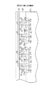
図1は本形態の半導体装置としてのゲートアレイ10を示す。ゲートアレイ10の半導体チップ11の中央部には内部セル領域12が形成され、この内部セル領域12にはpMOSトランジスタ及びnMOSトランジスタよりなる公知の基本セルが多数形成されており、一又は複数の基本セルを使用して種々の論理回路が構成される。
【0015】
半導体チップ11の周縁寄りには複数の外部パッド14がチップ11の周方向に並ぶように所定のピッチをもって配置され、これらの外部パッド14は図示しないボンディングワイヤ又はバンプによってパッケージの複数の入出力ピンと接続される。なお、パッドピッチはボンディング装置またはプローブ試験を行う試験装置の能力に基づいて決められる最小の値である。
【0016】
複数の入出力セル領域13は、複数の外部パッド14と内部セル領域12との間において半導体チップ11の周縁に沿うように形成されている。入出力セル領域13を使用して出力回路15が構成される。これらの入出力セル領域13の上方には低電位電源(VSS)を供給するための環状の電源配線31,32,33と、高電位電源(VDD)を供給するための環状の複数の電源配線34,35,36が設けられている。電源配線31,32,33及び電源配線34,35,36は金属配線層第1層に設けられている。
【0017】
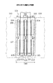
図2に示すように、入出力セル領域13は入出力回路を構成するための複数のトランジスタとしてのnMOSトランジスタ16及びpMOSトランジスタ17を備えている。本実施の形態ではnMOSトランジスタ16及びpMOSトランジスタ17はそれぞれ4個ずつ設けられている。
【0018】
それぞれ4個のnMOSトランジスタ16及びpMOSトランジスタ17は、半導体チップ11の周方向と直交する方向に並ぶように配置されている。各nMOSトランジスタ16はゲート16a、ソース16b及びドレイン16cの3つの電極を備え、これらゲート16a、ソース16b及びドレイン16cは半導体チップ11の周方向と直交する方向に並ぶように設けられている。各pMOSトランジスタ17はゲート17a、ソース17b及びドレイン17cの3つの電極を備え、これらゲート17a、ソース17b及びドレイン17cは半導体チップ11の周方向と直交する方向に並ぶように設けられている。
【0019】
各nMOSトランジスタ16のソース16b上を通過するように前記電源配線31,32,33が設けられている。nMOSトランジスタ16のソース16bは図示しない複数のコンタクトによって電源配線31,32,33に接続される。nMOSトランジスタ16のドレイン16c上には金属配線層第1層にアルミニウムよりなるドレイン配線20が設けられている。ドレイン配線20は複数のコンタクト21によってドレイン16cに接続されている。
【0020】
また、各pMOSトランジスタ17のソース17b上を通過するように前記電源配線34,35,36が設けられている。pMOSトランジスタ17のソース17bは図示しない複数のコンタクトによって電源配線34,35,36に接続される。pMOSトランジスタ17のドレイン17c上には金属配線層第1層にアルミニウムよりなるドレイン配線23が設けられている。ドレイン配線23は複数のコンタクト24によってドレイン17cに接続されている。
【0021】
入出力セル領域13上の金属配線層第2層には、入出力セル領域13の配置方向と直交するように延びるアルミニウム配線26が設けられている。アルミニウム配線26は図示しないコンタクトによって前記外部パッド14に接続される。アルミニウム配線26はコンタクト22によって前記ドレイン配線20に接続されるとともに、コンタクト25によって前記ドレイン配線23に接続されている。従って、各nMOSトランジスタ16及びpMOSトランジスタ17のドレインは、アルミニウム配線26を介して外部パッド14に接続される。
【0022】
図3は図2のA−A断面図であり、チップ基板41には1つのp型ウェル42及び1つのn型ウェル43が形成されている。p型ウェル42内にn+ 型のドレイン16b及びソース16cが交互に形成されている。チップ基板41上には絶縁層43が設けられ、ドレイン16b及びソース16c間の上方にはポリシリコンよりなるゲート16aが設けられている。n型ウェル43内にp+ 型のドレイン17b及びソース17cが交互に形成されている。絶縁層43には、ドレイン17b及びソース17c間の上方にポリシリコンよりなるゲート17aが設けられている。さらに、金属配線層第1層には前記電源配線31〜33,34〜36が設けられるとともに、ドレイン配線20,23が設けられている。金属配線層第2層には前記アルミニウム配線26が設けられている。
【0023】
本形態はこのように構成されているので、以下の効果がある。
(1)本形態の入出力セル領域13は、複数のnMOSトランジスタ16及びpMOSトランジスタ17を半導体チップ11の周方向と直交する方向に並ぶように配置するとともに、nMOSトランジスタ16及びpMOSトランジスタ17の3つの電極としてのゲート、ソース及びドレインを半導体チップ11の周方向と直交する方向に並ぶように設けた。そして、nMOSトランジスタ16に低電位電源を供給するための電源配線31〜33を金属配線層第1層に設けるとともに、pMOSトランジスタ17に高電位電源を供給するための電源配線34〜36を第1層の金属配線層に設け、入出力回路15の出力を外部パッド14に伝達するためのアルミニウム配線26を金属配線層第2層に設けた。そのため、各入出力セル領域13の上方における金属配線層第1層の配線領域の幅を縮小することができ、入出力セル領域13の配置ピッチを縮小することができる。よって、半導体チップ11の周方向に配置される入出力セル領域13の数が増加し、ゲートアレイ10の多ピン化を図ることができる。
【0024】
[第2の実施の形態]
次に、本発明の第2の実施の形態を図4,5に従って説明する。
図4に示すように、入出力セル領域50は入出力回路を構成するための複数のnMOSトランジスタ51及び複数のpMOSトランジスタ52を備えている。本実施の形態ではnMOSトランジスタ51及びpMOSトランジスタ52は入出力セル領域50の配置方向(図4において左右方向)、すなわち、半導体チップの周方向においてそれぞれ2列設けられ、入出力セル領域50の高さ方向(図4において上下方向)にそれぞれ6個ずつ設けられている。なお、図4において、MOSトランジスタのゲートがMOSトランジスタとして示されている。
【0025】
各nMOSトランジスタ51はゲート、ソース及びドレインの3つの電極を備え、これらゲート、ソース及びドレインは入出力セル領域50の高さ方向に並ぶように設けられている。各pMOSトランジスタ52はゲート、ソース及びドレインの3つの電極を備え、これらゲート、ソース及びドレインは入出力セル領域50の高さ方向に並ぶように設けられている。
【0026】
各nMOSトランジスタ51のソース上を通過するように金属配線層第1層に低電位電源(VSS)を供給するための電源配線53が設けられている。5個のnMOSトランジスタ51のドレイン上には金属配線層第1層にアルミニウムよりなるドレイン配線54が設けられている。ドレイン配線54は複数のコンタクト(実線で示す)によって対応するnMOSトランジスタ51のドレインに接続されている。また、上記5個のnMOSトランジスタ51のゲートは金属配線層第1層に設けられた信号線57に接続され、同信号線57には第1の信号線58を介して第1の信号IN1が入力される。第1の信号線58は金属配線層第2層に設けられたアルミニウム配線59,60と、金属配線層第1層に設けられたアルミニウム配線61とからなる。
【0027】
各pMOSトランジスタ52のソース上を通過するように金属配線層第1層に高電位電源(VDD)を供給するための電源配線55が設けられている。10個のpMOSトランジスタ52のドレイン上には金属配線層第1層にアルミニウムよりなるドレイン配線56が設けられている。ドレイン配線56は複数のコンタクト(実線で示す)によって対応するpMOSトランジスタ52のドレインに接続されている。また、上記10個のpMOSトランジスタ52のゲートは金属配線層第1層に設けられた信号線62に接続され、同信号線62には第2の信号線63を介して第2の信号IN2が入力される。第2の信号線63は金属配線層第2層に設けられたアルミニウム配線からなる。
【0028】
入出力セル領域50において、各列上の金属配線層第2層には、入出力セル領域50の高さ方向に延びるアルミニウム配線64が設けられている。アルミニウム配線64は破線で示すコンタクトによって図示しない外部パッドに接続される。アルミニウム配線64はコンタクト(破線で示す)によって前記ドレイン配線54,56に接続されている。従って、各nMOSトランジスタ51及びpMOSトランジスタ52のドレインは、アルミニウム配線64を介して外部パッドに接続される。
【0029】
図5は図4に示す入出力セル領域50に構成された出力回路の等価回路を示す。なお、5個のnMOSトランジスタ51は並列に接続されているため、図5においては5個のnMOSトランジスタ51は1個にまとめて図示されている。同様に、10個のpMOSトランジスタ52は並列に接続されているため、図5においては10個のpMOSトランジスタ52も1個にまとめて図示されている。
【0030】
本形態においても、前記第1の形態と同様の効果があるとともに、入出力セル領域50内の第1及び第2の信号線58,63はその大部分が金属配線層第2層に設けられており、電源配線53,55の影響を受けない。
【0031】
[第3の実施の形態]
次に、本発明の第3の実施の形態を図6,7に従って説明する。
図6に示すように、入出力セル領域70は入出力回路を構成するための複数のトランジスタとしてのnpnトランジスタ71及びpnpトランジスタ72を備えている。
【0032】
npnトランジスタ71及びpnpトランジスタ72は、入出力セル領域70の高さ方向(図6において上下方向)、すなわち、半導体チップの周方向と直交する方向に並ぶように配置されている。npnトランジスタ71はベースコンタクト71a、エミッタ71b及びコレクタコンタクト71cの3つの電極を備える。本形態において、ベースコンタクト71aは3つ、エミッタ71bは2つ、コレクタコンタクト71cは2つ設けられている。ベースコンタクト71a、エミッタ71b及びコレクタコンタクト71cは入出力セル領域70の高さ方向、すなわち、半導体チップの周方向と直交する方向に並ぶように配置されている。
【0033】
pnpトランジスタ72はベースコンタクト72a、エミッタコンタクト72b及びコレクタ72cの3つの電極を備える。本形態において、ベースコンタクト72aは3つ、エミッタコンタクト72bは2つ、コレクタ72cは2つ設けられている。ベースコンタクト72a、エミッタコンタクト72b及びコレクタ72cは入出力セル領域70の高さ方向、すなわち、半導体チップの周方向と直交する方向に並ぶように配置されている。
【0034】
npnトランジスタ71のエミッタ71b上を通過するように金属配線層第1層に低電位電源(VSS)を供給するための電源配線75が設けられている。npnトランジスタ71のエミッタ71bは図示しない複数のコンタクトによって電源配線75に接続される。2つのコレクタコンタクト71cの上方には金属配線層第1層にアルミニウムよりなるコレクタ配線76が設けられている。コレクタ配線76は複数のコンタクト78によってコレクタコンタクト71cに接続されている。3つのベースコンタクト71aの上方には金属配線層第1層にアルミニウムよりなるベース配線77が設けられている。npnトランジスタ71のベースコンタクト71aは図示しない複数のコンタクトによってベース配線77に接続される。
【0035】
pnpトランジスタ72のエミッタコンタクト72b上を通過するように金属配線層第1層に高電位電源(VDD)を供給するための電源配線80が設けられている。pnpトランジスタ72のエミッタコンタクト72bは図示しない複数のコンタクトによって電源配線80に接続される。2つのコレクタ72cの上方には金属配線層第1層にアルミニウムよりなるコレクタ配線81が設けられている。コレクタ配線81は複数のコンタクト83によってコレクタ72cに接続されている。3つのベースコンタクト72aの上方には金属配線層第1層にアルミニウムよりなるベース配線82が設けられている。pnpトランジスタ72のベースコンタクト72aは図示しない複数のコンタクトによってベース配線82に接続される。
【0036】
入出力セル領域70上の金属配線層第2層には、入出力セル領域70の配置方向と直交するように延びるアルミニウム配線85が設けられている。アルミニウム配線85は図示しないコンタクトによって外部パッド86に接続される。アルミニウム配線85はコンタクト79によって前記コレクタ配線76に接続されるとともに、コンタクト84によって前記コレクタ配線81に接続されている。従って、npnトランジスタ71のコレクタ及びpnpトランジスタ72のコレクタは、アルミニウム配線85を介して外部パッド86に接続される。
【0037】
図7は図6のB−B断面図であり、チップ基板91にはn型のコレクタ領域92内にp型のベース領域93が形成されている。コレクタ領域92にはn+ 型の2つのコレクタコンタクト71cが形成されている。ベース領域93内にp+ 型の3つのベースコンタクト71aとn+ 型のエミッタ71bとが交互に形成されている。また、チップ基板91にはp型のエミッタ領域94内にn型のベース領域95が形成されている。エミッタ領域94にはp+ 型の2つのエミッタコンタクト72bが形成されている。ベース領域95内にn+ 型の3つのベースコンタクト72aとp+ 型のコレクタ72cとが交互に形成されている。
【0038】
チップ基板91上には絶縁層96が設けられている。絶縁層96には、金属配線層第1層には前記電源配線75、コレクタ配線76、ベース配線77、電源配線80、コレクタ配線81及びベース配線82が設けられている。金属配線層第2層には前記アルミニウム配線85が設けられている。
【0039】
本形態はこのように構成されているので、以下の効果がある。
(1)本形態の入出力セル領域73は、npnトランジスタ71及びpnpトランジスタ72を半導体チップの周方向と直交する方向に並ぶように配置するとともに、npnトランジスタ71及びpnpトランジスタ72の3つの電極としてのベース、エミッタ及びコレクタを半導体チップの周方向と直交する方向に並ぶように設けた。そして、npnトランジスタ71に低電位電源を供給するための電源配線75を金属配線層第1層に設けるとともに、pnpトランジスタ72に高電位電源を供給するための電源配線80を第1層の金属配線層に設け、入出力回路の出力を外部パッド86に伝達するためのアルミニウム配線85を金属配線層第2層に設けた。そのため、入出力セル領域70の上方における金属配線層第1層の配線領域の幅を縮小することができ、入出力セル領域70の配置ピッチを縮小することができる。よって、半導体チップの周方向に配置される入出力セル領域70の数が増加し、ゲートアレイの多ピン化を図ることができる。
【0040】
なお、本発明は次のように任意に変更して具体化することも可能である。
(1)pMOSトランジスタ又はnMOSトランジスタのみを備えたMOSトランジスタ構成の入出力セル領域を備えた半導体装置に具体化してもよい。この場合にも、上記各実施の形態と同様の効果がある。
【0041】
(2)pnpトランジスタ又はnpnトランジスタのみを備えたバイポーラトランジスタ構成の入出力セル領域を備えた半導体装置に具体化してもよい。この場合にも、上記各実施の形態と同様の効果がある。
【0042】
(3)上記各形態では半導体装置としてのゲートアレイ10に具体化したが、複数の入出力セル領域が半導体チップの周縁に沿うように配置される形態の他のすべての半導体装置に具体化してもよい。
【0043】
【発明の効果】
以上詳述したように、本発明は、金属配線層第1層の配線領域の面積を縮小し、入出力セル領域の配置ピッチを縮小して、多ピン化を図ることができる。
【図面の簡単な説明】
【図1】第1の実施の形態の半導体装置を示すレイアウト図
【図2】第1の実施の形態の入出力セル領域の一例を示す平面図
【図3】図2のA−A線における断面図
【図4】第2の実施の形態の入出力セル領域の平面図
【図5】図4の出力回路の回路図
【図6】第3の実施の形態の入出力セル領域を示す平面図
【図7】図6のB−B線における断面図
【図8】従来の入出力セル領域を示す平面図
【符号の説明】
13,50,70 入出力セル領域
15 入出力回路
16,51 nMOSトランジスタ
17,52 pMOSトランジスタ
71 npnトランジスタ
72 pnpトランジスタ[0001]
BACKGROUND OF THE INVENTION
The present invention relates to a semiconductor device (IC), and more particularly to an input / output cell region.
In recent years, semiconductor devices have been highly integrated due to advances in manufacturing process technology, and an increase in the number of external pins is required in accordance with an increase in the number of circuits that can be formed on a semiconductor chip. In order to increase the number of pins of a semiconductor device, it is necessary to shorten the arrangement pitch of external pads for input / output arranged along the periphery of the semiconductor chip. At the same time, the width of the input / output cell region for configuring the input / output circuit arranged along the periphery of the semiconductor chip inside the external pad, that is, the length in the arrangement direction of the input / output cell region is shortened. It is necessary.
[0002]
[Prior art]
One form of IC is a gate array. FIG. 8 shows an
[0003]
The gates, sources, and drains, which are the three electrodes of the four
[0004]
On the source of each
[0005]
[Problems to be solved by the invention]
However, in the input /
[0006]
In addition, it is necessary to avoid the
[0007]
As a result, the arrangement pitch per input /
[0008]
The present invention has been made to solve the above-described problems, and its object is to reduce the area of the wiring area of the first layer of the metal wiring layer and reduce the arrangement pitch of the input / output cell areas. An object of the present invention is to provide a semiconductor device that can be pinned.
[0009]
[Means for Solving the Problems]
To achieve the above object, the invention of
[0010]
According to a second aspect of the present invention , the plurality of transistors include an nMOS transistor and a pMOS transistor .
According to a third aspect of the invention , the metal wiring is connected to each drain of the nMOS transistor and the pMOS transistor .
[0011]
According to a fourth aspect of the present invention , the plurality of transistors include an npn transistor and a pnp transistor .
According to a fifth aspect of the present invention , the metal wiring is connected to each collector of the npn transistor and the pnp transistor .
According to a sixth aspect of the present invention , each of the plurality of transistors includes three electrodes, and the three electrodes are a source, a drain, and a gate .
According to a seventh aspect of the present invention , each of the plurality of transistors includes three electrodes, and the three electrodes are a base, an emitter, and a collector .
According to an eighth aspect of the present invention , each of the semiconductor chips includes a first wiring layer and a second wiring layer which are arranged along the circumferential direction of the semiconductor chip and are stacked on each other, and the source of the nMOS transistor And a power supply wiring connected to the source of the pMOS transistor are formed in the first wiring layer, and are connected in common to the drain of the nMOS transistor and the drain of the pMOS transistor. A metal wiring is formed in the second wiring layer .
[0012]
(Function)
According to the invention of claim 1-8, the power source wiring for supplying power to the plurality of transistors of each output cell area in the first wiring layer, connecting the pads corresponding to each output cell region by providing a metal wiring for the first second wiring layer laminated on the upper wiring layer, it is possible to reduce the wiring width of the first wiring layer. As a result, the width of the input / output cell region along the circumferential direction of the semiconductor chip can be reduced, and the arrangement pitch of the input / output cell region can be reduced to increase the number of pins.
[0013]
DETAILED DESCRIPTION OF THE INVENTION
[First Embodiment]
Hereinafter, a first embodiment of the present invention will be described with reference to FIGS.
[0014]
FIG. 1 shows a
[0015]
Near the periphery of the
[0016]
The plurality of input /
[0017]
As shown in FIG. 2, the input /
[0018]
Each of the four
[0019]
The
[0020]
The
[0021]
In the second layer of the metal wiring layer on the input /
[0022]
FIG. 3 is a cross-sectional view taken along the line AA of FIG. 2. One p-
[0023]
Since the present embodiment is configured as described above, the following effects are obtained.
(1) In the input /
[0024]
[Second Embodiment]
Next, a second embodiment of the present invention will be described with reference to FIGS.
As shown in FIG. 4, the input /
[0025]
Each
[0026]
A
[0027]
A
[0028]
In the input /
[0029]
FIG. 5 shows an equivalent circuit of the output circuit configured in the input /
[0030]
In this embodiment, the same effect as that of the first embodiment is obtained, and most of the first and
[0031]
[Third Embodiment]
Next, a third embodiment of the present invention will be described with reference to FIGS.
As shown in FIG. 6, the input /
[0032]
The
[0033]
The
[0034]
A
[0035]
A
[0036]
In the second metal wiring layer on the input /
[0037]
FIG. 7 is a cross-sectional view taken along the line B-B of FIG. 6. A p-
[0038]
An insulating
[0039]
Since the present embodiment is configured as described above, the following effects are obtained.
(1) In the input / output cell region 73 of this embodiment, the
[0040]
It should be noted that the present invention can be arbitrarily modified and embodied as follows.
(1) The present invention may be embodied in a semiconductor device including an input / output cell region having a MOS transistor configuration including only a pMOS transistor or an nMOS transistor. Also in this case, the same effects as those of the above embodiments are obtained.
[0041]
(2) The present invention may be embodied in a semiconductor device including an input / output cell region having a bipolar transistor configuration including only a pnp transistor or an npn transistor. Also in this case, the same effects as those of the above embodiments are obtained.
[0042]
(3) Although the above embodiments are embodied in the
[0043]
【The invention's effect】
As described in detail above, the present invention can reduce the area of the wiring region of the first layer of the metal wiring layer and reduce the arrangement pitch of the input / output cell regions, thereby achieving a high pin count.
[Brief description of the drawings]
FIG. 1 is a layout diagram showing a semiconductor device according to a first embodiment. FIG. 2 is a plan view showing an example of an input / output cell region according to the first embodiment. FIG. 4 is a plan view of the input / output cell region of the second embodiment. FIG. 5 is a circuit diagram of the output circuit of FIG. 4. FIG. 6 is a plan view of the input / output cell region of the third embodiment. FIG. 7 is a sectional view taken along line BB in FIG. 6. FIG. 8 is a plan view showing a conventional input / output cell region.
13, 50, 70 Input /
Claims (8)
前記複数のパッドに対応し、前記半導体チップの周方向に並ぶように配置された複数の入出力セル領域と、
を備えた半導体装置において、
前記複数の入出力セル領域の各々は、前記半導体チップの周方向と直交する方向に並ぶように配置された複数のトランジスタを含み、
前記複数のトランジスタの各々に電源を供給するための電源配線を前記半導体チップの周方向に沿って第1の配線層に設け、
前記複数のトランジスタを該複数のトランジスタを含む前記入出力セル領域に対応する前記パッドに接続するための金属配線を前記第1の配線層の上方に積層された第2の配線層に設けた、
ことを特徴とする半導体装置。 A plurality of pads arranged along the outer periphery of the semiconductor chip;
A plurality of input / output cell regions corresponding to the plurality of pads and arranged in a circumferential direction of the semiconductor chip ;
In a semiconductor device comprising:
Each of the plurality of input / output cell regions includes a plurality of transistors arranged in a direction orthogonal to a circumferential direction of the semiconductor chip,
A power supply wiring for supplying power to each of the plurality of transistors is provided in the first wiring layer along the circumferential direction of the semiconductor chip,
Metal wiring for connecting the plurality of transistors to the pad corresponding to the input / output cell region including the plurality of transistors is provided in a second wiring layer stacked above the first wiring layer.
Wherein a.
ことを特徴とする請求項1に記載の半導体装置。 The plurality of transistors include an nMOS transistor and a pMOS transistor.
The semiconductor device according to claim 1 .
ことを特徴とする請求項2に記載の半導体装置。 The metal wiring is connected to the drain of each of the nMOS transistor and the pMOS transistor.
The semiconductor device according to claim 2, characterized in that.
ことを特徴とする請求項1に記載の半導体装置。 The plurality of transistors include an npn transistor and a pnp transistor,
The semiconductor device according to claim 1, characterized in that.
ことを特徴とする請求項4に記載の半導体装置。 The metal wiring is connected to collectors of the npn transistor and the pnp transistor,
The semiconductor device according to claim 4, characterized in that.
前記3つの電極は、ソース、ドレイン及びゲートである、
ことを特徴とする請求項1に記載の半導体装置。 Each of the plurality of transistors includes three electrodes,
The three electrodes are a source, a drain and a gate,
The semiconductor device according to claim 1, characterized in that.
前記3つの電極は、ベース、エミッタ及びコレクタである、
ことを特徴とする請求項1に記載の半導体装置。 Each of the plurality of transistors includes three electrodes,
The three electrodes are a base, an emitter and a collector,
The semiconductor device according to claim 1, characterized in that.
前記nMOSトランジスタのソースに接続されている電源配線及び前記pMOSトランジスタのソースに接続されている電源配線が前記第1の配線層に形成されており、
前記nMOSトランジスタのドレインと前記pMOSトランジスタのドレインに共通に接続されている金属配線が前記第2の配線層に形成されている、
ことを特徴とする請求項2に記載の半導体装置。 Each of the semiconductor chips includes a first wiring layer and a second wiring layer that are arranged along the circumferential direction of the semiconductor chip and stacked on each other,
A power supply line connected to the source of the nMOS transistor and a power supply line connected to the source of the pMOS transistor are formed in the first wiring layer;
A metal wiring commonly connected to the drain of the nMOS transistor and the drain of the pMOS transistor is formed in the second wiring layer;
The semiconductor device according to claim 2, characterized in that.
Priority Applications (4)
| Application Number | Priority Date | Filing Date | Title |
|---|---|---|---|
| JP25176596A JP3962441B2 (en) | 1996-09-24 | 1996-09-24 | Semiconductor device |
| US08/859,036 US5903019A (en) | 1996-09-24 | 1997-05-20 | Semiconductor device having a plurality of input/output cell areas with reduced pitches therebetween |
| KR1019970023724A KR100260345B1 (en) | 1996-09-24 | 1997-06-10 | Semiconductor device |
| TW086106802A TW337614B (en) | 1996-09-24 | 1997-09-27 | A semiconductor device |
Applications Claiming Priority (1)
| Application Number | Priority Date | Filing Date | Title |
|---|---|---|---|
| JP25176596A JP3962441B2 (en) | 1996-09-24 | 1996-09-24 | Semiconductor device |
Publications (2)
| Publication Number | Publication Date |
|---|---|
| JPH1098108A JPH1098108A (en) | 1998-04-14 |
| JP3962441B2 true JP3962441B2 (en) | 2007-08-22 |
Family
ID=17227590
Family Applications (1)
| Application Number | Title | Priority Date | Filing Date |
|---|---|---|---|
| JP25176596A Expired - Lifetime JP3962441B2 (en) | 1996-09-24 | 1996-09-24 | Semiconductor device |
Country Status (4)
| Country | Link |
|---|---|
| US (1) | US5903019A (en) |
| JP (1) | JP3962441B2 (en) |
| KR (1) | KR100260345B1 (en) |
| TW (1) | TW337614B (en) |
Families Citing this family (9)
| Publication number | Priority date | Publication date | Assignee | Title |
|---|---|---|---|---|
| JP3989038B2 (en) * | 1996-04-17 | 2007-10-10 | 株式会社ルネサステクノロジ | Semiconductor integrated circuit device |
| JP3914649B2 (en) * | 1999-02-10 | 2007-05-16 | 株式会社東芝 | Semiconductor device |
| US6696712B1 (en) * | 2000-08-11 | 2004-02-24 | Seiko Epson Corporation | Semicustom IC having adjacent macrocells |
| JP2001339047A (en) * | 2000-05-29 | 2001-12-07 | Matsushita Electric Ind Co Ltd | Semiconductor device |
| JP4798881B2 (en) * | 2001-06-18 | 2011-10-19 | 富士通セミコンダクター株式会社 | Semiconductor integrated circuit device |
| US7217966B1 (en) * | 2005-02-18 | 2007-05-15 | National Semiconductor Corporation | Self-protecting transistor array |
| US7594198B2 (en) * | 2007-02-27 | 2009-09-22 | Taiwan Semiconductor Manufacturing Co., Ltd. | Ultra fine pitch I/O design for microchips |
| US9972624B2 (en) | 2013-08-23 | 2018-05-15 | Qualcomm Incorporated | Layout construction for addressing electromigration |
| US9786663B2 (en) * | 2013-08-23 | 2017-10-10 | Qualcomm Incorporated | Layout construction for addressing electromigration |
Family Cites Families (6)
| Publication number | Priority date | Publication date | Assignee | Title |
|---|---|---|---|---|
| US5300796A (en) * | 1988-06-29 | 1994-04-05 | Hitachi, Ltd. | Semiconductor device having an internal cell array region and a peripheral region surrounding the internal cell array for providing input/output basic cells |
| JPH02152254A (en) * | 1988-12-02 | 1990-06-12 | Mitsubishi Electric Corp | Semiconductor integrated circuit device |
| JP3185271B2 (en) * | 1991-09-13 | 2001-07-09 | 日本電気株式会社 | Semiconductor integrated circuit |
| JP3228583B2 (en) * | 1992-03-31 | 2001-11-12 | 株式会社東芝 | Semiconductor integrated circuit device |
| JP2822781B2 (en) * | 1992-06-11 | 1998-11-11 | 三菱電機株式会社 | Master slice type semiconductor integrated circuit device |
| JPH06326194A (en) * | 1993-05-17 | 1994-11-25 | Mitsubishi Electric Corp | Semiconductor integrated circuit device |
-
1996
- 1996-09-24 JP JP25176596A patent/JP3962441B2/en not_active Expired - Lifetime
-
1997
- 1997-05-20 US US08/859,036 patent/US5903019A/en not_active Expired - Lifetime
- 1997-06-10 KR KR1019970023724A patent/KR100260345B1/en not_active IP Right Cessation
- 1997-09-27 TW TW086106802A patent/TW337614B/en not_active IP Right Cessation
Also Published As
| Publication number | Publication date |
|---|---|
| JPH1098108A (en) | 1998-04-14 |
| KR100260345B1 (en) | 2000-07-01 |
| KR19980024049A (en) | 1998-07-06 |
| US5903019A (en) | 1999-05-11 |
| TW337614B (en) | 1998-08-01 |
Similar Documents
| Publication | Publication Date | Title |
|---|---|---|
| US4893168A (en) | Semiconductor integrated circuit device including bonding pads and fabricating method thereof | |
| KR920008396B1 (en) | Semiconductor integrated circuit device | |
| US5060046A (en) | Semiconductor integrated circuit device having enlarged cells formed on ends of basic cell arrays | |
| JPH03165061A (en) | Semiconductor integrated circuit device | |
| US4771327A (en) | Master-slice integrated circuit having an improved arrangement of transistor elements for simplified wirings | |
| JP3962441B2 (en) | Semiconductor device | |
| US7595561B2 (en) | Semiconductor device including multiple rows of peripheral circuit units | |
| JPH02152254A (en) | Semiconductor integrated circuit device | |
| JPH07118507B2 (en) | Semiconductor integrated circuit using bump mounting | |
| JP4017060B2 (en) | Semiconductor device | |
| JP2000252363A (en) | Semiconductor integrated circuit | |
| JPS586157A (en) | Cmos master slice lsi | |
| KR0129126B1 (en) | Semiconductor integrated circuit device | |
| JP3211871B2 (en) | I / O protection circuit | |
| JPH0122736B2 (en) | ||
| JPH0562469B2 (en) | ||
| JPH0787240B2 (en) | Semiconductor integrated circuit | |
| JPS62263653A (en) | Manufacture of semiconductor integrated circuit device | |
| JPS6329545A (en) | Semiconductor integrated circuit device | |
| JPH02310946A (en) | Semiconductor integrated circuit device | |
| JPH0245957A (en) | Semiconductor integrated circuit device | |
| JP3038896B2 (en) | Semiconductor device | |
| KR920005798B1 (en) | Borderless master slice semiconductor device | |
| JPH0831524B2 (en) | Semiconductor integrated circuit device | |
| JPH098227A (en) | Semiconductor integrated circuit device |
Legal Events
| Date | Code | Title | Description |
|---|---|---|---|
| A977 | Report on retrieval |
Free format text: JAPANESE INTERMEDIATE CODE: A971007 Effective date: 20040114 |
|
| A131 | Notification of reasons for refusal |
Free format text: JAPANESE INTERMEDIATE CODE: A131 Effective date: 20040203 |
|
| A521 | Written amendment |
Free format text: JAPANESE INTERMEDIATE CODE: A523 Effective date: 20040405 |
|
| A131 | Notification of reasons for refusal |
Free format text: JAPANESE INTERMEDIATE CODE: A131 Effective date: 20050208 |
|
| A521 | Written amendment |
Free format text: JAPANESE INTERMEDIATE CODE: A523 Effective date: 20050411 |
|
| A711 | Notification of change in applicant |
Free format text: JAPANESE INTERMEDIATE CODE: A711 Effective date: 20050830 |
|
| A131 | Notification of reasons for refusal |
Free format text: JAPANESE INTERMEDIATE CODE: A131 Effective date: 20060808 |
|
| RD04 | Notification of resignation of power of attorney |
Free format text: JAPANESE INTERMEDIATE CODE: A7424 Effective date: 20060814 |
|
| A521 | Written amendment |
Free format text: JAPANESE INTERMEDIATE CODE: A523 Effective date: 20061010 |
|
| TRDD | Decision of grant or rejection written | ||
| A01 | Written decision to grant a patent or to grant a registration (utility model) |
Free format text: JAPANESE INTERMEDIATE CODE: A01 Effective date: 20070515 |
|
| A61 | First payment of annual fees (during grant procedure) |
Free format text: JAPANESE INTERMEDIATE CODE: A61 Effective date: 20070521 |
|
| R150 | Certificate of patent or registration of utility model |
Free format text: JAPANESE INTERMEDIATE CODE: R150 |
|
| S111 | Request for change of ownership or part of ownership |
Free format text: JAPANESE INTERMEDIATE CODE: R313111 |
|
| FPAY | Renewal fee payment (event date is renewal date of database) |
Free format text: PAYMENT UNTIL: 20100525 Year of fee payment: 3 |
|
| R350 | Written notification of registration of transfer |
Free format text: JAPANESE INTERMEDIATE CODE: R350 |
|
| FPAY | Renewal fee payment (event date is renewal date of database) |
Free format text: PAYMENT UNTIL: 20100525 Year of fee payment: 3 |
|
| FPAY | Renewal fee payment (event date is renewal date of database) |
Free format text: PAYMENT UNTIL: 20110525 Year of fee payment: 4 |
|
| FPAY | Renewal fee payment (event date is renewal date of database) |
Free format text: PAYMENT UNTIL: 20110525 Year of fee payment: 4 |
|
| S531 | Written request for registration of change of domicile |
Free format text: JAPANESE INTERMEDIATE CODE: R313531 |
|
| S533 | Written request for registration of change of name |
Free format text: JAPANESE INTERMEDIATE CODE: R313533 |
|
| FPAY | Renewal fee payment (event date is renewal date of database) |
Free format text: PAYMENT UNTIL: 20110525 Year of fee payment: 4 |
|
| R350 | Written notification of registration of transfer |
Free format text: JAPANESE INTERMEDIATE CODE: R350 |
|
| FPAY | Renewal fee payment (event date is renewal date of database) |
Free format text: PAYMENT UNTIL: 20120525 Year of fee payment: 5 |
|
| FPAY | Renewal fee payment (event date is renewal date of database) |
Free format text: PAYMENT UNTIL: 20120525 Year of fee payment: 5 |
|
| FPAY | Renewal fee payment (event date is renewal date of database) |
Free format text: PAYMENT UNTIL: 20130525 Year of fee payment: 6 |
|
| FPAY | Renewal fee payment (event date is renewal date of database) |
Free format text: PAYMENT UNTIL: 20140525 Year of fee payment: 7 |
|
| S111 | Request for change of ownership or part of ownership |
Free format text: JAPANESE INTERMEDIATE CODE: R313111 |
|
| R350 | Written notification of registration of transfer |
Free format text: JAPANESE INTERMEDIATE CODE: R350 |
|
| EXPY | Cancellation because of completion of term |