JP3961985B2 - Organic electroluminescence device - Google Patents
Organic electroluminescence device Download PDFInfo
- Publication number
- JP3961985B2 JP3961985B2 JP2003150772A JP2003150772A JP3961985B2 JP 3961985 B2 JP3961985 B2 JP 3961985B2 JP 2003150772 A JP2003150772 A JP 2003150772A JP 2003150772 A JP2003150772 A JP 2003150772A JP 3961985 B2 JP3961985 B2 JP 3961985B2
- Authority
- JP
- Japan
- Prior art keywords
- layer
- organic
- hole injection
- electrode layer
- injection electrode
- Prior art date
- Legal status (The legal status is an assumption and is not a legal conclusion. Google has not performed a legal analysis and makes no representation as to the accuracy of the status listed.)
- Expired - Fee Related
Links
Images

Classifications
-
- H—ELECTRICITY
- H10—SEMICONDUCTOR DEVICES; ELECTRIC SOLID-STATE DEVICES NOT OTHERWISE PROVIDED FOR
- H10K—ORGANIC ELECTRIC SOLID-STATE DEVICES
- H10K50/00—Organic light-emitting devices
- H10K50/80—Constructional details
- H10K50/805—Electrodes
- H10K50/81—Anodes
- H10K50/816—Multilayers, e.g. transparent multilayers
-
- H—ELECTRICITY
- H10—SEMICONDUCTOR DEVICES; ELECTRIC SOLID-STATE DEVICES NOT OTHERWISE PROVIDED FOR
- H10K—ORGANIC ELECTRIC SOLID-STATE DEVICES
- H10K2102/00—Constructional details relating to the organic devices covered by this subclass
- H10K2102/301—Details of OLEDs
- H10K2102/331—Nanoparticles used in non-emissive layers, e.g. in packaging layer
Landscapes
- Physics & Mathematics (AREA)
- Optics & Photonics (AREA)
- Electroluminescent Light Sources (AREA)
Description
【0001】
【発明の属する技術分野】
本発明は、発光を素子の両側から取り出すことができる、耐久性に優れた有機エレクトロルミネッセンス素子に関する。
【0002】
【従来の技術】
電界発光を利用したエレクトロルミネッセンス素子(以下、EL素子と略記する)は、自己発光のため視認性が高く、かつ完全固体素子であるため、耐衝撃性に優れるなどの特徴を有することから、各種表示装置における発光素子としての利用が注目されている。
【0003】
EL素子には、発光材料として無機化合物を用いる無機EL素子と、有機化合物を用いる有機EL素子とがあり、このうち、有機EL素子は、印加電圧を大幅に低くし得るので小型化が容易であり、そのため次世代の表示素子としてその実用化研究が積極的になされている。有機EL素子の構成は、下部電極/発光層/対向電極の構成を基本とし、ガラス板等を用いた基板上に、下部電極を設ける構成が通常採用されている。この場合、発光は基板側に取り出される。
【0004】
ところで、近年以下の理由で、対向電極を透明にして発光を対向電極側に取り出す試みがなされている。
(ア)下部電極を透明とすれば、透明な発光素子ができる。
(イ)透明な発光素子の背景色として任意の色が採用でき、発光時以外もカラフルなディスプレイとすることができ、装飾性が改良される。又、背景色として黒を採用した場合には、発光時のコントラストが向上する。
【0005】
(ウ)カラーフィルターや色変換層を用いる場合は、発光素子の上にこれらを置くことができる。このため、これらの層を考慮することなく素子を製造することができる。その利点として、例えば、下部電極を形成させる際に基板温度を高くすることができ、これにより下部電極の抵抗値を下げることができる。対向電極を透明にすることにより、前記のような利点が得られるため、透明な対向電極を用いた有機EL素子を作成する試みがなされている。
【0006】
特許文献1には、透明導電層よりなる下部電極と、超薄膜の電子注入金属層及びその上に形成される透明導電層よりなる対向電極を設けた、透明な有機EL素子が開示されている。前記公報には、これらの透明導電層を構成する物質として、ITO(インジウムチンオキサイド)やSnO2 が開示されている。しかし、これらはX線回折ピークが消失する程度にまで結晶性を低減することはできず、本質的に結晶質である。このため、有機層を介して基板に積層するに際して、有機層の損傷を防ぐために基板温度を室温〜100℃近くに設定して蒸着した場合、比抵抗値の高い透明導電層が形成される(ITOでは、1×10⁻³Ω・cm程度以上となる)。そして、そのような有機EL素子においては、透明導電層の配線ラインで電圧降下が発生し、発光に不均一性が生じるため、比抵抗値を下げる等の改良が求められている。その上、ITOやSnO2 は、本質的に結晶質であるため、結晶粒界より水分や酸素が侵入し易い。このため、隣接して積層される電子注入金属層が劣化を受け易く、その結果発光欠陥が生じたり、発光しなくなったりする等、耐久性が十分とは言えず、更なる改良が求められている。
【0007】
又、別の技術として、直接、有機層に透明導電層である酸化物膜をスパッタリングにて形成し対向電極とする場合がある。しかしながら、この方法では、スパッタリング時に発生する酸素プラズマにより有機層が損傷を受け、良好な性能が発揮できないという問題がある。
【特許文献1】
特開平8−185984号公報
【0008】
【発明が解決しようとする課題】
本発明の目的は、上記従来技術の課題を解決し、低抵抗かつ高透明の対向電極を有する有機EL素子を提供することにある。又、対向電極を構成する透明導電膜から水分や酸素が侵入しにくく、耐久性に優れ、更に、透明導電膜の形成時に有機層が損傷を受けない構成の陽極を有する有機EL素子を提供することにある。
【0009】
【課題を解決するための手段】
本発明者らは、上記課題を解決するために鋭意研究を重ねた結果、対向電極を構成する透明導電膜として非晶質の透明導電膜を採用することにより、上記の課題が解決されることを見出した。本発明は、かかる知見に基づいて完成させたものである。
【0010】
即ち、本発明の要旨は以下の通りである。
(1)下部電極である陰極と、前記陰極の対向電極である陽極との間に有機発光層を含む有機層が介在してなる有機エレクトロルミネッセンス素子であって、前記陽極が正孔注入電極層と非晶質透明導電膜とからなり、かつ前記正孔注入電極層が前記有機層と接することを特徴とする有機エレクトロルミネッセンス素子であって、前記正孔注入電極層が、正孔注入性のカーボンを用いて、膜厚0.5〜20nmの超薄膜状に形成され、前記陰極が、陽極酸化法により作製されてなるAl2 O3 又はAlOX (1<x≦3/2)を電子注入電極層として含むことを特徴とする有機エレクトロルミネッセンス素子。
(2)正孔注入電極層が、正孔注入性のカーボンと正孔伝達性の有機物の混合層であることを特徴とする前記(1)記載の有機エレクトロルミネッセンス素子。
【0012】
(3)正孔注入電極層が、不連続に形成され有機層の表面を覆いつくしていない島状正孔注入域からなることを特徴とする前記(1)記載の有機エレクトロルミネッセンス素子。
(4)非晶質透明導電膜が、インジウム(In)、亜鉛(Zn)、酸素(O)からなる酸化物を用いて、形成されていることを特徴とする前記(1)〜(3)のいずれかに記載の有機エレクトロルミネッセンス素子。
(5)前記正孔注入電極層が、膜厚0.5〜7nmの超薄膜状に形成されている前記(1)〜(4)のいずれかに記載の有機エレクトロルミネッセンス素子。
(6)前記正孔注入電極層の光線透過率が50%以上である前記(1)〜(5)のいずれかに記載の有機エレクトロルミネッセンス素子。
【0013】
【発明の実施の形態】
以下、本発明を詳細に説明する。本発明の有機EL素子は、下部電極と対向電極との間に有機発光層を含む有機層が介在しており、対向電極は正孔注入電極層と非晶質透明導電膜とによって構成されており、しかも正孔注入電極層が有機層と接するという構成である。この構成は、例えば、図1により模式的に表すことができる。以下に、これらの構成について説明する。
【0014】
<非晶質透明導電膜>
先ず、本発明の有機EL素子において対向電極を構成する非晶質透明導電膜について説明する。本発明で用いる非晶質透明導電膜は、非晶質であって透明性を有するものであればよいが、前記したように、電圧降下とそれに起因する発光の不均一性を排除するため、比抵抗値が5×10⁻⁴Ω・cm以下であることが好ましい。
【0015】
又、材質としては、In−Zn−O系の酸化物膜が好ましい。ここで、In−Zn−O系の酸化物膜とは、主要カチオン元素としてインジウム(In)及び亜鉛(Zn)を含有する非晶質酸化物からなる透明導電膜のことである。Inの原子比〔In/(In+Zn)〕は0.45〜0.90が好ましい。なぜならば、この範囲外では導電性が低くなる可能性があるからである。Inの原子比〔In/(In+Zn)〕は、導電性の観点からは0.50〜0.90が特に好ましく、0.70〜0.85が更に好ましい。
【0016】
上記非晶質酸化物は、主要カチオン元素として実質的にIn及びZnのみを含有するものであってもよいし、その他に価数が正3価以上の1種以上の第3元素を含有するものであってもよい。前記第3元素の具体例としては、スズ(Sn)、アルミニウム(Al)、アンチモン(Sb)、ガリウム(Ga)、ゲルマニウム(Ge)、チタン(Ti)等が挙げられるが、導電性の向上という観点からは、Snを含有するものが特に好ましい。又、第3元素の含有量は、その総量の原子比[(全第3元素)/〔In+Zn+(全第3元素)〕]が0.2以下となる量が好ましい。第3元素の総量の原子比が0.2を超えると、イオンの散乱により導電性が低くなる場合がある。この第3元素の総量の特に好ましい原子比は0.1以下である。尚、組成が同じであっても、結晶化したものは非晶質のものより導電性に劣るので、この点からも非晶質の透明導電膜を使用する必要がある。
【0017】
上述の非晶質酸化物は、薄膜にすることで透明導電膜として利用可能となる。この時の膜厚は、概ね3〜3000nmとするのが好ましい。なぜならば、3nm未満では導電性が不十分となり易く、3000nmを超えると光透過性が低下したり、有機EL素子を製造する過程や製造後において、故意又は不可避的に有機EL素子を変形させた時に透明導電膜にクラック等が生じ易くなるからである。この透明導電膜の特に好ましい膜厚は5〜1000nmであり、更に好ましい膜厚は10〜800nmである。
【0018】
本発明の有機EL素子において、基板上に下部電極及び有機層を介して対向電極が形成される場合、正孔注入電極層の上に非晶質透明導電膜(酸化膜)が形成される。非晶質透明導電膜の形成手法としては、スパッタリング法の他、化学蒸着法、ゾルゲル法、イオンプレーティング法等を採用できるが、有機層への熱的な影響が少ないことや簡便性の観点より、スパッタリング法が好ましい。この場合、スパッタリング時に発生するプラズマにより有機層が損傷を受けないように注意する必要がある。又、有機層の耐熱性は低いので、基板の温度を200℃以下とするのが好ましい。
【0019】
スパッタリングの方法は、RFあるいはDCマグネトロンスパッタリング等でも反応性スパッタリングでもよく、使用するスパッタリングターゲットの組成やスパッタリングの条件は、成膜しようとする透明導電膜の組成等に応じて適宜選択される。RFあるいはDCマグネトロンスパッタリング等によりIn−Zn−O系の透明導電膜を形成させる場合には、下記(i)、(ii)のスパッタリングターゲットを用いることが好ましい。
【0020】
(i)酸化インジウムと酸化亜鉛との組成物からなる焼結体ターゲットで、インジウムの原子比が所定のもの。ここで、「インジウムの原子比が所定のもの」とは、最終的に得られる膜におけるInの原子比〔In/(In+Zn)〕が0.45〜0.90の範囲内の所望値となるものを意味するが、焼結体ターゲットにおける原子比が概ね0.50〜0.90のものである。この焼結体ターゲットは、酸化インジウムと酸化亜鉛との混合物からなる焼結体であってもよいし、In2 O3 (ZnO)m (m=2〜20)で表される六方晶層状化合物の1種以上から実質的になる焼結体であってもよいし、In2 O3 (ZnO)m (m=2〜20)で表される六方晶層状化合物の1種以上とIn2 O3 及び/又はZnOとから実質的になる焼結体であってもよい。尚、六方晶層状化合物を表す前記式においてmを2〜20に限定する理由は、mが前記範囲外では六方晶層状化合物とならないからである。
【0021】
(ii)酸化物系ディスクと、このディスク上に配置した1種以上の酸化物系タブレットとからなるスパッタリングターゲット。酸化物系ディスクは、酸化インジウム又は酸化亜鉛から実質的になるものであってもよいし、In2 O3 (ZnO)m (m=2〜20)で表される六方晶層状化合物の1種以上から実質的になる焼結体であってもよいし、In2 O3 (ZnO)m (m=2〜20)で表される六方晶層状化合物の1種以上とIn2 O3 及び/又はZnOとから実質的になる焼結体であってもよい。又、酸化物系タブレットとしては、上記酸化物系ディスクと同様のものを使用することができる。酸化物系ディスク及び酸化物系タブレットの組成並びに使用割合は、最終的に得られる膜におけるInの原子比〔In/(In+Zn)〕が0.45〜0.80の範囲内の所望値となるように適宜決定される。
【0022】
前記(i)、(ii)のいずれのスパッタリングターゲットもその純度は98%以上であることが好ましい。スパッタリングターゲットの純度が98%未満では、不純物の存在により、得られる膜の耐湿熱性(耐久性)が低下したり、導電性が低下したり、光透過性が低下したりすることがある。より好ましい純度は99%以上であり、更に好ましい純度は99.9%以上である。
【0023】
又、焼結体ターゲットを用いる場合、このターゲットの相対密度は70%以上とすることが好ましい。相対密度が70%未満では、成膜速度の低下や膜質の低下を招き易い。より好ましい相対密度は85%以上であり、更に好ましくは90%以上である。ダイレクトスパッタリング法により透明導電膜を設ける場合のスパッタリング条件は、ダイレクトスパッタリングの方法やスパッタリングターゲットの組成、用いる装置の特性等により種々変わってくるため、一概に規定することは困難であるが、DCダイレクトスパッタリング法による場合には例えば下記のように設定することが好ましい。
【0024】
スパッタリング時の真空度及びターゲット印加電圧は次のように設定することが好ましい。即ち、スパッタリング時の真空度は1.3×10⁻² 〜6.7×100 Pa程度、より好ましくは1.7×10⁻²〜1.3×100 Pa程度、更に好ましくは4.0×10⁻²〜6.7×10⁻¹Pa程度とする。又、ターゲットの印加電圧は200〜500Vが好ましい。スパッタリング時の真空度が1.3×10⁻²Paに満たない(1.3×10⁻²Paよりも圧力が低い)とプラズマの安定性が悪く、6.7×100 Paよりも高い(6.7×100 Paよりも圧力が高い)とスパッタリングターゲットへの印加電圧を高くすることができなくなる。又、ターゲット印加電圧が200V未満では、良質の薄膜を得るのが困難になったり、成膜速度が制限されることがある。
【0025】
雰囲気ガスとしては、アルゴンガス等の不活性ガスと酸素ガスとの混合ガスが好ましい。不活性ガスとしてアルゴンガスを用いる場合、このアルゴンガスと酸素ガスとの混合比(体積比)は概ね1:1〜99.99:0.01、好ましくは9:1〜99.9:0.1とする。この範囲を外れると、低抵抗かつ光線透過率の高い膜が得られない場合がある。
【0026】
基板温度は、有機層の耐熱性に応じて、当該有機層が熱により変形や変質を起こさない温度の範囲内で適宜選択される。基板温度が室温未満では冷却用の機器が別途必要になるため、製造コストが上昇する。又、基板温度を高温に加熱する場合、別途そのための加熱処理装置が必要になるため、製造コストが上昇する。このため、基板温度は室温〜200℃とするのが好ましい。
【0027】
前記した(i)、(ii)のスパッタリングターゲットを用いて、上述したような条件でダイレクトスパッタリングを行うことにより、目的とする透明導電膜を有機層上に設けることができる。
【0028】
<正孔注入電極層>
次に、正孔注入電極層について説明する。正孔注入電極層とは、発光層を含む有機層に良好に正孔注入ができる電極の層であり、透明発光素子を得るためには、光線透過率が50%以上であることが好ましく、これを達成するためには膜厚を0.5〜20nm程度の超薄膜とすることが望ましい。
【0029】
正孔注入電極層としては、例えば、仕事関数4.8eV以上の金属(正孔注入性の金属)、例えば、Pt、Ni、Pd、Os等を用いて、膜厚を1〜20nmとした層を挙げることができる。この場合において、50%以上、特に60%以上の光線透過率を与える構成が好ましい。他の好ましい例としては、前記の仕事関数4.8eV以上の金属(複数種でもよい)と他の金属との合金(正孔注入性の合金)を用いた正孔注入電極層を挙げることができる。このような合金としては、正孔注入電極層の形成が可能な合金であれば足りるが、例えば、金−インジウム合金、金−アルミニウム合金、インジウム−白金合金、鉛−金合金、ビスマス−金合金、スズ−金合金、アルミニウム−白金合金、アルミニウム−ニッケル合金、アルミニウム−パラジウム合金を挙げることができる。この場合においても、膜厚を1〜20nmとすることが好ましく、50%以上、特に60%以上の光線透過率を与える層とすることが好ましい。
【0030】
前記の金属又は合金を用いて正孔注入電極層を形成させる場合、好適には抵抗加熱蒸着法又は電子ビーム蒸着法を用いる。この場合、基板温度を10〜100℃の間で設定し、蒸着速度を0.05〜20nm/秒の間に設定するのが好ましい。又、特に合金を蒸着する場合には、2元蒸着法を用い、2種の金属の蒸着速度を個別に設定して蒸着することができる。この場合、Pt、Ni、Pd、Au等の蒸着速度を0.01〜0.1nm/秒の間に設定し、In等の他の金属の蒸着速度を1〜10nm/秒の間に設定して同時に蒸着するという手法が採用できる。又、合金を蒸着する場合に、1元蒸着法を用いることもできる。この場合、予め所望の割合で正孔注入性の金属を母体金属に仕込んだ蒸着ペレット又は粒状体を抵抗加熱ボートやフィラメントに設置し、加熱蒸着する。
【0031】
更に別の好ましい形態としては、薄膜状の正孔注入性のカーボンであって、膜厚が0.1〜20nmの超薄膜を挙げることができる。前記カーボンとしては、例えば、グラファイト、非晶質カーボンを好ましいものとして挙げることができる。カーボン層の形成手法としては、アーク放電蒸着法によりカーボンを蒸着する方法を採用することもできる。
【0032】
尚、これまで説明した、正孔注入性の金属、合金、カーボンについては、1種のみでなく2種以上を用いて正孔注入電極層を形成することもできる。更に他の好ましい例として、正孔注入電極層は、正孔注入性の金属、合金あるいはカーボンと正孔伝達性の化合物との混合層であってもよい。正孔注入性の金属、合金、カーボンとしては、前記した金属、合金、カーボンを挙げることができる。又、これらは、1種のみでなく2種以上を用いることもできる。一方、正孔伝達性の化合物は、正孔を伝達する化合物であればよく、好ましい化合物として、一種の正孔輸送芳香族第三アミンを含有しているものである。この、芳香族第三アミンは、炭素原子(その内の一つは芳香環の環員である)にのみ結合している少なくとも一個の三価の窒素原子を有する化合物である。これらの一態様として、芳香族第三アミンは、モノアリールアミン、ジアリールアミン、トリアリールアミン又は高分子アリールアミン等のアリールアミンが挙げられる。低分子トリアリールアミンは、クラプフル等(Klupfel et. al. )による米国特許第3,180,730号公報に開示されている。ビニルあるいはビニレンラジカルで置換され、そして/又は少なくとも一個の水素含有基を含有している他の適当なトリアリールアミンは、ブラントレイ等(Brantley et. al.)による米国特許第3,567,450号公報及び米国特許第3,658,520号公報に開示されている。好ましい種類の芳香族第三アミンは、少なくとも二個のアミン成分を含むものである。このような化合物としては、以下の構造式[I] で表されるものが挙げられる。
【0033】
【化1】

式中、Q1 及びQ2 は各々独立した芳香族第三アミン成分であり、Gは、アリレーン基、シクロアルキレン基、アルキレン基、又は炭素−炭素結合を表している。構造式[I] を満足し、そして2個のトリアリール成分を含有する、特に好ましい種類のトリアリールアミンは、以下の構造式[II]を満足するものである。
【0035】
【化2】
式中、R1 及びR2 は、各々独立した水素原子、アリール基又はアルキル基を表すか、あるいはR1 とR2 が結合してシクロアルキル基を完成している基を表し、R3 及びR4 は、各々独立して以下の構造式[III] で示されるようなジアリール置換アミノ基で置換されたアリール基を表す。
【0037】
【化3】
式中、R5 及びR6 は、各々独立して選択されたアリール基である。別の好ましい種類の芳香族第三アミンとしては、テトラアリールジアミンが挙げられる。このテトラアリールジアミンは、アリーレン基を介して結合した構造式[III] で表されるジアリール基を2個含むことが好ましい。好ましいテトラアリーレンジアミンとしては、以下の構造式[IV]により表されるものが挙げられる。
【0039】
【化4】
式中、Areはアリーレン基であり、nは1〜4の整数であり、Ar、R7 、R8 及びR9 は独立して選択されたアリール基である。上記の構造式[I] 、[II]、[III] 、及び[IV]の種々のアルキル、アルキレン、アリール及びアリーレン成分は、各々置換されていてもよい。典型的な置換基としては、例えば、アルキル基、アルコキシ基、アリール基、アリールオキシ基並びにフッ素、塩素及び臭素等のハロゲンが挙げられる。種々のアルキル及びアルキレン成分は、典型的には、炭素数が約1〜6である。シクロアルキル成分の炭素数は約3〜10であるが、典型的には、5個、6個又は7個の環炭素原子を含み、例えば、シクロペンチル、シクロヘキシル及びシクロヘプチル環構造を有しているものである。アリール及びアリーレン成分は、フェニル及びフェニレン構造であることが好ましい。
【0041】
又、正孔注入性の金属、合金、カーボンと正孔伝達性の化合物との混合比(重量比)は、100:1〜1:100とすることが好ましい。正孔注入性の金属、合金及び電子伝達性の化合物との混合層は、2元同時蒸着法により形成するのが好ましい。その時の基板温度は、10〜100℃の間で設定すればよい。
【0042】
更に他の好ましい例として、正孔注入電極層が島状の正孔注入域である構成を挙げることができる。ここで、島状とは、例えば図2に示すように、不連続に正孔注入性化合物層が形成されていて、この層は有機層の表面を覆いつくすことがないことを意味する。島状正孔注入域は、例えば仕事関数4.8eV以上の高仕事関数の金属、酸化物、合金、カーボン等を島状に不連続に形成させたものであり、その形状及び大きさについては特に制限はないが、微粒子状又は結晶状であって、大きさが0.5nm〜5μm程度のものが好ましい。
【0043】
又、この正孔注入域は、薄膜状を指すものでも、孤立原子分散の状態を示すものでもない。上記の高仕事関数の金属又は化合物が、粒子状の形態で導電性薄膜上又は有機化合物層内に分散されている状態を指す。上記島状正孔注入域を構成する高仕事関数の金属及び合金としては、仕事関数4.8eV以上のものが好ましく、例えば、前記した金属及び合金を挙げることができる。又、高仕事関数の酸化物としては、酸化ニッケル、酸化マンガンが好ましい。
【0044】
島状正孔注入域の形成方法としては、抵抗加熱蒸着法や電子ビーム蒸着法を採用することができる。後者の場合、高融点の酸化物やカーボンを電子ビーム蒸着により島状に不連続に形成させる。本発明の有機EL素子においては、対向電極である陽極が正孔注入電極層と非晶質透明導電膜とで構成されているため、非晶質透明導電膜の形成時に正孔注入電極層が損傷を受けることより有機層が保護される。この結果として良好な有機EL素子を作製できる。
【0045】
又、正孔注入電極層が有機層と接することで、正孔が有機層に注入される。これにより、下部電極である陰極側からの電子の注入とあいまってEL素子へ良好に電荷注入がなされる。本発明の有機EL素子においては、通常、基板上に下部電極である陰極を積層し、その上に有機層を積層する構成を採用するが、この場合、有機発光層を含む有機層の上に正孔注入電極層を形成する。形成方法は、前記の通りであり、他の好ましい方法としてスパッタリング法があるが、この手法を用いるに際しては、プラズマにより有機層が損傷を受けないように注意する必要がある。
【0046】
他の好ましい正孔注入電極層としては、導電性のポリマー、例えば全共役系ポリマーである、ポリアリーレンビニレン、ポリチオフェン、ポリチェニレンビニレン、ポリアニリン等も用いることができる。
【0047】
<有機層>
本発明の有機EL素子において、陽極と陰極との間に介在する有機層は、少なくとも発光層を含む。有機層は、発光層のみからなる層であってもよく、又、発光層とともに、正孔注入輸送層等を積層した多層構造のものであってもよい。
【0048】
この有機EL素子において、発光層は(1)電界印加時に、陽極又は正孔輸送層により正孔を注入することができ、かつ電子注入層より電子を注入することができる機能、(2)注入した電荷(電子と正孔)を電界の力で移動させる輸送機能、(3)電子と正孔の再結合の場を発光層内部に提供し、これを発光につなげる発光機能等を有している。この発光層に用いられる発光材料の種類については特に制限はなく、従来から知られている有機EL素子において公知のものを用いることができる。
【0049】
又、正孔注入輸送層は、正孔伝達化合物からなる層であって、陽極より注入された正孔を発光層に伝達する機能を有し、この正孔注入輸送層を陽極と発光層との間に介在させることにより、より低い電界で多くの正孔が発光層に注入される。その上、電子注入層より発光層に注入された電子は、発光層と正孔注入輸送層の界面に存在する電子の障壁により、この発光層内の界面近くに蓄積されたEL素子の発光効率を向上させ、その結果発光性能の優れたEL素子となる。この正孔注入輸送層に用いられる正孔伝達化合物については特に制限はなく、従来から有機EL素子において使用されてきた、正孔伝達化合物として公知のものを使用することができる。正孔注入輸送層は、単層のみでなく多層とすることもできる。
【0050】
<陰極>
次に、陰極について説明する。陰極とは、発光層を含む有機層に良好に電子注入ができる電極の層であり、透明発光素子を得るためには、光線透過率が50%以上であることが好ましく、このためには膜厚を0.5〜20nm程度の超薄膜とすることが望ましい。
【0051】
陰極としては、例えば、仕事関数3.8eV以下の金属(電子注入性の金属)、例えば、Mg、Ca、Ba、Sr、Li、Yb、Eu、Y、Sc等を用いて膜厚を1〜500nmとした層を挙げることができる。この場合において、50%以上、特に60%以上の光線透過率を与える構成が望ましい時には、膜厚を1〜20nmとすることが必要である。
【0052】
他の好ましい例としては、前記の仕事関数3.8eV以下の金属(複数種でもよい)と仕事関数4.0eV以上の金属との合金(電子注入性の合金)を用いた電子注入電極層を挙げることができる。このような合金としては、電子注入電極層の形成が可能な合金であれば足りるが、例えば、アルミニウム−リチウム合金、マグネシウム−アルミニウム合金、インジウム−リチウム合金、鉛−リチウム合金、ビスマス−リチウム合金、スズ−リチウム合金、アルミニウム−カルシウム合金、アルミニウム−バリウム合金、アルミニウム−スカンジウム合金等を挙げることができる。この場合においても、膜厚を1〜20nmとすることで、50%以上、特に60%以上の光線透過率を与える層とすることができる。
【0053】
前記の金属又は合金を用いて陰極を形成させる場合、好適には抵抗加熱蒸着法を用いる。この場合、基板温度を10〜100℃の間で設定し、蒸着速度を0.05〜20nm/秒の間に設定するのが好ましい。又、特に合金を蒸着する場合には、2元蒸着法を用い、2種の金属の蒸着速度を個別に設定して蒸着するすることができる。この場合、Li、Ba、Ca、Sc、Mg等の蒸着速度を0.01〜0.1nm/秒の間に設定し、Al等の母体金属の蒸着速度を1〜10nm/秒の間に設定して同時に蒸着するという手法が採用できる。又、合金を蒸着する場合に、1元蒸着法を用いることもできる。この場合、予め所望の割合で電子注入性の金属を母体金属に仕込んだ蒸着ペレット又は粒状体を抵抗加熱ボートやフィラメントに設置し、加熱蒸着する。
【0054】
更に別の好ましい形態としては、薄膜状の電子注入性のアルカリ土類金属酸化物、アルカリ酸化物又はアルカリフッ化物であって、膜厚が0.1〜10nmの超薄膜を挙げることができる。前記アルカリ土類金属酸化物としては、例えば、BaO、SrO、CaO及びこれらを混合したBax Sr1-x O(0<x <1)や、BaXCa1-XO(0<x <1)を好ましいものとして挙げることができる。アルカリ酸化物又はアルカリフッ化物としては、LiF、Li2O、NaF等が挙げられる。
【0055】
アルカリ土類金属酸化物層の形成手法としては、抵抗加熱蒸着法によりアルカリ土類金属を蒸着しながら、真空槽内に酸素を導入して真空度を10-3〜10-4Paとし、酸素とアルカリ土類金属を反応させながら蒸着させる方法が好ましい。又、アルカリ土類金属酸化物を電子ビーム蒸着法により製膜する方法を採用することできる。
【0056】
アルカリ酸化物の形成方法としては、上記アルカリ土類金属酸化物の形成方法と同様の方法を用いることができる。アルカリフッ化物の形成方法としては、電子ビーム蒸着法又は、抵抗加熱蒸着法が挙げられる。尚、これまで説明した、電子注入性の金属、合金、アルカリ土類金属酸化物については、1種のみでなく2種以上を用いて電子注入電極層を形成することもできる。
【0057】
更に好ましい例としては、Al2 O3 又はAlOX (1<x ≦3/2)が挙げられる。この作製方法としては、Alの自然酸化、プラズマによる酸化が挙げられる。この他の作製方法としては、Al2 O3 を電子ビーム蒸着する方法、真空槽内に酸素を導入して真空度を10-3〜10-4Paとし、酸素とAlを反応させながら蒸着させる方法が好ましい。
【0058】
又、更に好ましい方法は、Alを電解質液中でこれを陽極として、通電、酸化する陽極酸化法が挙げられる。陽極酸化法の詳細な条件としては、クエン酸、リン酸、ホウ酸アンモニウム、酒石酸アンモニウムの希釈溶液中で、前記のAlを陽極とし、白金等の貴金属を陰極として、5〜300Vの電圧を定電流で通電する。この時、pHを調整し、pH6〜8の範囲に保つことにより作製すると、緻密なAlOX (1<x ≦3/2)ができる。
【0059】
<有機EL素子の構成>
本発明の有機EL素子は、陽極と陰極との間に有機発光層を含む有機層が介在しており、陽極は正孔注入電極層と非晶質透明導電膜とによって構成され、しかも正孔注入電極層が有機層と接するという構成を具備していれば、本発明の目的を達成することができるが、更に他の構成を付加して、種々の機能を持たせることができる。以下に本発明の有機EL素子を利用した構成を例示する。
【0060】
(1) 透明陰極/有機層/正孔注入電極層/非晶質透明電極
(2) 陰極/有機層/正孔注入電極層/非晶質透明電極/カラーフィルター
(3) 陰極/有機層/正孔注入電極層/非晶質透明電極/色変換層
(4) 透明陰極/有機層/正孔注入電極層/非晶質透明電極/黒色光吸収層
(5) 透明陰極/有機層/正孔注入電極層/非晶質透明電極/背景色形成層
(6) 黒色光吸収層/透明陰極/有機層/正孔注入電極層/非晶質透明電極
(7) 背景色形成層/透明陰極/有機層/正孔注入電極層/非晶質透明電極前記
(8) の構成の場合、両方の電極が透明なので、透明表示素子が形成される。
【0061】
前記(2) や(3) の構成の場合、陰極を支持基板上に形成し、支持基板とは逆方向に発光の取り出しができるので、カラーフィルターや色変換層上に陽極を形成する必要がない。従って、陰極を形成する際に基板温度が150℃以上となるようなプロセスを採用することができ、形成する陰極によっては高温プロセスの採用に限定される場合や、陰極の抵抗値を下げる面で大きなメリットがある。又、カラーフィルターや色変換層は陰極形成後に形成されるため、高温プロセスの採用による劣化を心配する必要がない。図3に、前記(2) の構成を例示する。尚、ここで、色変換層としては、蛍光性色素を含有する透明性ポリマーからなり、EL発光色を蛍光により別の色に変換するものであることが好ましい。
【0062】
又、前記(2) や(3) の構成で、多くの画素を構成させた態様においては、基板上に陽極以外の補助配線やTFT(Thin Film Transister)が形成されるため、基板方向に光を取り出すと、補助配線やTFTが光を遮断し、光取り出しの開口率が落ち、結果としてディスプレイの輝度が小さくなり、画質が落ちるという欠点がある。それ故、本発明を用いれば基板とは逆の方向に光の取り出しができ、この場合には光が遮断されず光取り出しの開口率が落ちないという効果がある。
【0063】
【実施例】
以下、本発明を実施例に基づき詳細に説明するが、本発明はこれらの例によって何ら限定されるものではない。
〔実施例1〕
<有機EL素子の作製>
25mm×75mm×1mmのガラス基板上に、ITOを100nmの膜厚で製膜したもの(ジオマティックス社製)を、基板上に導電性薄膜が成膜してあるものとして使用した。次に、これをイソプロピルアルコール中に浸漬し、超音波洗浄を行った後、サムコインターナショナル製の紫外線照射機UV−300を用いて紫外線とオゾンとを併用して30分間洗浄した。
【0064】
次に、真空蒸着装置にてAlを15nmの膜厚で蒸着した。次いで、0.1モル/リットルの酒石酸アンモニウム水溶液とエチレングリコールを1:9の容量比で混合し、これに少量のアンモニウム水溶液を添加して調整した溶液に、上記のAlを形成したガラス基板を浸漬し、これを陽極として陽極酸化した。尚、陽極酸化は生成する酸化膜の膜厚が3nmとなるよう電圧を4〜6Vに設定した。これにより、ITO上にAl/酸化アルミニウムの陰極が形成された。
【0065】
次に、この基板をイソプロピルアルコール中に浸漬し、超音波洗浄を行った後、上記と同じ紫外線照射機UV−300(サムコインターナショナル製)にて紫外線とオゾンを併用し、5分間洗浄した。上記基板を真空蒸着装置の基板ホルダーに取り付け、8−キノリノールアルミニウム錯体(以下Alqと略記する)を60nm蒸着した。次に、N,N’−ビス(3−メチルフェニル)−N,N’−ジフェニル−(1,1’−ビフェニル)−4,4’−ジアミン(以下TPDと略記する)を20nm蒸着した。次に、4,4’−ビス−(N,N−ジ−m−トリルアミノ)−4”−フェニル−トリフェニルアミン(以下TPD74と略記する)を80nm蒸着した。ここで、Alq、TPD、TPD74は各々、発光層、正孔輸送層、正孔注入層としての機能を果たす。次に、カーボンをアーク放電蒸着により10nm蒸着した。このカーボンは、正孔注入電極層としての機能を果たす。
【0066】
次に、上記真空蒸着装置に連結されている別の真空槽の基板ホルダーに基板を移送しセットした。尚、この間真空度は保たれたままである。上記、別の真空槽はDCマグネトロンスパッタリングによりIn−Zn−O系酸化物膜を形成できるように設備されている。In−Zn−O系酸化物膜を形成させるためのターゲットは、In2 O3 とZnOとからなる焼結体であり、Inの原子比〔In/(In+Zn)〕は0.67である。この真空槽のアルゴンガスと酸素ガスの混合ガス(体積比で1000:2.8)を3×10-1Paとなるまで導入し、スパッタリング出力を100W、基板温度を室温に設定して膜厚200nmの非晶質透明導電膜を形成させた。尚、In−Zn−O系酸化物膜が非晶質であることは、ITO薄膜が蒸着されていないガラス基板を用いて上記と同様の方法により積層体を形成し、X線回折により確認した。
【0067】
次に有機EL素子を評価した。先ず、非晶質透明導電膜について、三菱油化株式会社製のロレスタFPを用いた四探針法により面抵抗値を調べたところ、23Ω/□であった。そして、膜厚が200nmであるから、比抵抗値は、4.6×10-4Ω・cmと低いことが確認された。次に、ITO/Al/酸化アルミニウムを陰極として、前記カーボン層/In−Zn−O透明導電膜を陽極として、電圧を7V印加したところ、2.0mA/cm2 の電流密度となり、非晶質透明導電膜側より観測したところ、輝度70Cd/m2 の発光があった。この発光は、Alqより生じた緑色発光であった。
【0068】
更に、この素子を大気中、70%RH(相対湿度)の雰囲気に500時間放置したところ、無発光点は目視では観測されず、素子の発光性能も維持されていた。本発明の透明陽極は、空気中の水分、酸素に対しても耐性のあることが判った。
【0069】
〔比較例1〕
実施例1と同様の方法により有機EL素子を作製した。但し、In−Zn−O系酸化物膜を形成させる代わりに、In−Sn−O系酸化物(ITO)をDCマグネトロンスパッタリングで結晶質透明導電膜であるところのITO膜を形成させた。
【0070】
その後、実施例1と同様の方法により有機EL素子の性能を評価したところ、面抵抗値は300Ω/□と大きな値を示した。そして、膜厚が200nmであるから、比抵抗値は、6×10-3Ω・cmと高いことが確認された。次に、ITO/Al/酸化アルミニウムを陰極として、前記カーボン層/In−Sn−O透明導電膜を陽極として、この有機EL素子に電圧を8V印加したところ、2.4mA/cm2 の電流密度となり、非晶質透明導電膜側より観測したところ、輝度60Cd/m2 の発光があった。この発光は、Alqより生じた緑色発光であった。
【0071】
この素子を大気中、70%RH(相対湿度)の雰囲気に500時間放置したところ、無発光点は目視で多数(3000個/cm2 以上)確認され、発光欠陥の多いことが確認された。更に、基板温度が室温の場合、結晶質であるITO基板は高い抵抗値を示し、これを1mm程度以下に細線化して発光させると、輝度が不均一化することが判った。
【0072】
〔比較例2〕
実施例1と同様の方法により有機EL素子を作製した。但し、カーボン(正孔注入電極層)は形成しないで、直接In−Zn−O透明導電膜をTPD74上に製膜した。
【0073】
実施例1と同様の方法により有機EL素子の性能を評価したところ、非晶質透明導電膜の面抵抗値は、25Ω/□と実施例1の場合とほぼ同じであった。そして、膜厚が200nmであるから、比抵抗値の面では、4×10-4Ω・cmと優れていることが確認された。次に、ITO/Al/酸化アルミニウムを陰極として、前記In−Zn−O透明導電膜を陽極として、この有機EL素子に電圧を7V印加したが、電流密度は0.2mA/cm2 と実施例1に比べて低い値を示した。又、非晶質透明導電膜側より観測したところ、輝度70Cd/m2 を与える電流量が4.0mA/cm2 と大きくなり、効率が著しく低下した。この理由は、In−Zn−OのDCマグネトロンスパッタリング時に、プラズマによる損傷をTPD74が受けているためと考えられる。正孔注入電極層はプラズマダメージ(特に酸素プラズマと想定される)を防ぐために必要であることが判った。
【0080】
〔実施例2〕
正孔伝達性の化合物であるTPD74とカーボンを蒸着法にて、重量比1:1で混合し、正孔注入電極層とした以外は、実施例1と同様の方法により有機EL素子を作製した。
【0081】
実施例1と同様の方法により有機EL素子を評価した。即ち、ITO/Al/酸化アルミニウムを陰極として、カーボンとTPD74の混合層/In−Zn−O透明導電膜を陽極として、電圧を7V印加したところ電流密度は2.1mA/cm2 、輝度は78Cd/m2 であった。そして、対向電極の面抵抗値は21Ω/□であった。
【0082】
又、実施例1と同様に大気中放置テストを行ったが、無発光点は目視では観測できず、発光性能は維持されていた。次に、ITO/Al/酸化アルミニウムを陰極とし、カーボンとTPD74の混合層/In−Zn−O透明導電膜を陽極とし、電圧を8V印加したところ、3.8mA/cm2 の電流密度となった。そして、非晶質透明導電膜側より観測したところ、輝度65Cd/m2 の発光があった。この発光は、Alqより生じた緑色発光であった。
【0083】
更に、この素子を大気中、70%RHの雰囲気に500時間放置したところ、無発光点は目視では観測されず、素子の発光効率も落ちず、発光性能が維持されていた。
【0084】
【発明の効果】
本発明の有機EL素子は、低抵抗かつ高透明の陽極を有するため、発光を効率よく素子の両面から取り出すことができる。又、耐久性に優れる。このため、本発明の有機EL素子は、例えば情報機器のディスプレイ等に好適に用いられる。
【図面の簡単な説明】
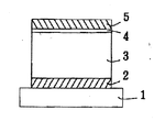
【図1】 本発明の有機EL素子の一例の構成を示す断面図である。
【図2】 本発明の有機EL素子において、島状正孔注入域が、非晶質透明導電膜と有機層との界面に存在する場合の一例の構成を示す断面図である。
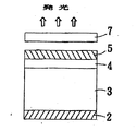
【図3】 本発明の有機EL素子の利用態様の一例を単純化して示したものであって、非晶質透明導電膜の外側にカラーフィルターを付加した構成を示す断面図である。
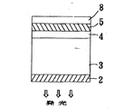
【図4】 本発明の有機EL素子の利用態様の一例を単純化して示したものであって、非晶質透明導電膜の外側に黒色吸収層を備えた構成を示す断面図である。
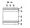
【図5】 本発明の有機EL素子の利用態様の一例を単純化して示したものであって、透明陰極の外側に背景色形成層を備えた構成を示す断面図である。
【符号の説明】
1:基板
2:陰極(下部電極)
3:有機層
4:正孔注入電極層
5:非晶質透明導電膜
6:島状注入域
7:カラーフィルター
8:黒色光吸収層
9:背景色形成層[0001]
BACKGROUND OF THE INVENTION
The present invention relates to an organic electroluminescence device having excellent durability that can extract light emitted from both sides of the device.
[0002]
[Prior art]
An electroluminescence element utilizing electroluminescence (hereinafter abbreviated as EL element) has high visibility due to self-emission and is a completely solid element, and therefore has characteristics such as excellent impact resistance. The use as a light emitting element in a display device has attracted attention.
[0003]
EL elements include inorganic EL elements that use inorganic compounds as light emitting materials and organic EL elements that use organic compounds. Among these, organic EL elements can be significantly reduced in size because the applied voltage can be significantly reduced. For this reason, research into practical use as a next-generation display element has been actively conducted. The configuration of the organic EL element is basically the configuration of the lower electrode / light emitting layer / counter electrode, and a configuration in which the lower electrode is provided on a substrate using a glass plate or the like is usually employed. In this case, the emitted light is extracted to the substrate side.
[0004]
By the way, in recent years, attempts have been made to extract the emitted light to the counter electrode side by making the counter electrode transparent.
(A) If the lower electrode is transparent, a transparent light emitting element can be produced.
(A) Any color can be adopted as the background color of the transparent light-emitting element, and a colorful display can be obtained even when light is emitted, and the decorativeness is improved. In addition, when black is used as the background color, the contrast during light emission is improved.
[0005]
(C) When a color filter or a color conversion layer is used, these can be placed on the light emitting element. For this reason, an element can be manufactured without considering these layers. As an advantage thereof, for example, the substrate temperature can be increased when the lower electrode is formed, thereby reducing the resistance value of the lower electrode. Since the advantages described above can be obtained by making the counter electrode transparent, an attempt has been made to produce an organic EL element using the transparent counter electrode.
[0006]
[0007]
As another technique, there is a case where an oxide film, which is a transparent conductive layer, is directly formed on the organic layer by sputtering to form a counter electrode. However, this method has a problem that the organic layer is damaged by oxygen plasma generated during sputtering, and good performance cannot be exhibited.
[Patent Document 1]
JP-A-8-185984
[Problems to be solved by the invention]
An object of the present invention is to solve the above-described problems of the prior art and to provide an organic EL element having a low resistance and highly transparent counter electrode. Also provided is an organic EL device having an anode having a structure in which moisture and oxygen hardly enter from the transparent conductive film constituting the counter electrode, has excellent durability, and the organic layer is not damaged when the transparent conductive film is formed. There is.
[0009]
[Means for Solving the Problems]
As a result of intensive studies to solve the above problems, the present inventors have solved the above problems by adopting an amorphous transparent conductive film as the transparent conductive film constituting the counter electrode. I found. The present invention has been completed based on such knowledge.
[0010]
That is, the gist of the present invention is as follows.
(1) An organic electroluminescence device in which an organic layer including an organic light emitting layer is interposed between a cathode as a lower electrode and an anode as a counter electrode of the cathode, wherein the anode is a hole injection electrode layer And an amorphous transparent conductive film, and the hole injection electrode layer is in contact with the organic layer, wherein the hole injection electrode layer has a hole injection property. Carbon is used to form Al 2 O 3 or AlO x (1 <x ≦ 3/2), which is formed into an ultrathin film having a film thickness of 0.5 to 20 nm and the cathode is made by an anodic oxidation method. An organic electroluminescence device comprising an injection electrode layer.
(2) The organic electroluminescence device as described in (1) above, wherein the hole injection electrode layer is a mixed layer of a hole injection carbon and a hole transfer organic substance.
[0012]
(3) hole-injection electrode layer is discontinuously formed above, wherein the formed of island-shaped hole injection zone that is not exhausted covers the surface of the organic layer (1) Symbol placement of the organic electroluminescent device.
( 4 ) The amorphous transparent conductive film is formed using an oxide made of indium (In), zinc (Zn), and oxygen (O), (1) to ( 3 ) above An organic electroluminescence device according to any one of the above.
( 5 ) The organic electroluminescence device according to any one of (1) to ( 4 ), wherein the hole injection electrode layer is formed in an ultrathin film having a thickness of 0.5 to 7 nm.
( 6 ) The organic electroluminescence device according to any one of (1) to ( 5 ), wherein the light transmittance of the hole injection electrode layer is 50% or more.
[0013]
DETAILED DESCRIPTION OF THE INVENTION
Hereinafter, the present invention will be described in detail. In the organic EL device of the present invention, an organic layer including an organic light emitting layer is interposed between a lower electrode and a counter electrode, and the counter electrode is constituted by a hole injection electrode layer and an amorphous transparent conductive film. In addition, the hole injection electrode layer is in contact with the organic layer. This configuration can be schematically represented by, for example, FIG. Below, these structures are demonstrated.
[0014]
<Amorphous transparent conductive film>
First, the amorphous transparent conductive film constituting the counter electrode in the organic EL element of the present invention will be described. The amorphous transparent conductive film used in the present invention only needs to be amorphous and transparent, but as described above, in order to eliminate voltage drop and non-uniformity of light emission resulting therefrom, The specific resistance value is preferably 5 × 10 −4 Ω · cm or less.
[0015]
As a material, an In—Zn—O-based oxide film is preferable. Here, the In—Zn—O-based oxide film is a transparent conductive film made of an amorphous oxide containing indium (In) and zinc (Zn) as main cation elements. The atomic ratio [In / (In + Zn)] of In is preferably 0.45 to 0.90. This is because the conductivity may be low outside this range. The atomic ratio [In / (In + Zn)] of In is particularly preferably 0.50 to 0.90 and more preferably 0.70 to 0.85 from the viewpoint of conductivity.
[0016]
The amorphous oxide may substantially contain only In and Zn as main cation elements, and may contain one or more third elements having a valence of at least positive trivalence. It may be a thing. Specific examples of the third element include tin (Sn), aluminum (Al), antimony (Sb), gallium (Ga), germanium (Ge), titanium (Ti), and the like. From the viewpoint, those containing Sn are particularly preferable. The content of the third element is preferably such that the atomic ratio [(total third elements) / [In + Zn + (total third elements)]] of the total amount is 0.2 or less. When the atomic ratio of the total amount of the third element exceeds 0.2, the conductivity may be lowered due to ion scattering. A particularly preferable atomic ratio of the total amount of the third element is 0.1 or less. Even if the composition is the same, the crystallized one is inferior in conductivity to the amorphous one, and it is necessary to use an amorphous transparent conductive film also from this point.
[0017]
The amorphous oxide described above can be used as a transparent conductive film by forming a thin film. The film thickness at this time is preferably about 3 to 3000 nm. This is because if the thickness is less than 3 nm, the electrical conductivity tends to be insufficient, and if it exceeds 3000 nm, the light transmittance is lowered, or the organic EL device is intentionally or inevitably deformed during or after the process of manufacturing the organic EL device. This is because sometimes a crack or the like is likely to occur in the transparent conductive film. A particularly preferable film thickness of this transparent conductive film is 5 to 1000 nm, and a more preferable film thickness is 10 to 800 nm.
[0018]
In the organic EL device of the present invention, when the counter electrode is formed on the substrate via the lower electrode and the organic layer, an amorphous transparent conductive film (oxide film) is formed on the hole injection electrode layer. As a method for forming the amorphous transparent conductive film, in addition to the sputtering method, a chemical vapor deposition method, a sol-gel method, an ion plating method, and the like can be adopted. However, there is little thermal influence on the organic layer and the viewpoint of simplicity. A sputtering method is more preferable. In this case, care must be taken so that the organic layer is not damaged by the plasma generated during sputtering. In addition, since the heat resistance of the organic layer is low, the temperature of the substrate is preferably 200 ° C. or lower.
[0019]
The sputtering method may be RF or DC magnetron sputtering or reactive sputtering. The composition of the sputtering target used and the sputtering conditions are appropriately selected according to the composition of the transparent conductive film to be formed. When an In—Zn—O based transparent conductive film is formed by RF or DC magnetron sputtering or the like, it is preferable to use the following sputtering targets (i) and (ii).
[0020]
(I) A sintered compact target made of a composition of indium oxide and zinc oxide, having an indium atomic ratio of a predetermined value. Here, “the atomic ratio of indium is a predetermined one” means that the In atomic ratio [In / (In + Zn)] in the finally obtained film is a desired value within the range of 0.45 to 0.90. This means that the atomic ratio of the sintered compact target is approximately 0.50 to 0.90. The sintered body target may be a sintered body made of a mixture of indium oxide and zinc oxide, or a hexagonal layered compound represented by In 2 O 3 (ZnO) m (m = 2 to 20). In addition, one or more of the hexagonal layered compounds represented by In 2 O 3 (ZnO) m (m = 2 to 20) and In 2 O may be used. It may be a sintered body substantially composed of 3 and / or ZnO. In the above formula representing the hexagonal layered compound, m is limited to 2 to 20 because m is not a hexagonal layered compound outside the above range.
[0021]
(Ii) A sputtering target comprising an oxide disk and one or more oxide tablets arranged on the disk. The oxide-based disk may be substantially composed of indium oxide or zinc oxide, or one of hexagonal layered compounds represented by In 2 O 3 (ZnO) m (m = 2 to 20). It may be a sintered body substantially consisting of the above, or one or more of hexagonal layered compounds represented by In 2 O 3 (ZnO) m (m = 2 to 20), In 2 O 3 and / or Alternatively, it may be a sintered body substantially composed of ZnO. Moreover, as an oxide type tablet, the thing similar to the said oxide type disc can be used. The composition and usage ratio of the oxide-based disk and the oxide-based tablet are desired values within the range where the atomic ratio [In / (In + Zn)] of In in the finally obtained film is 0.45 to 0.80. As appropriate.
[0022]
The purity of any of the sputtering targets (i) and (ii) is preferably 98% or more. If the purity of the sputtering target is less than 98%, due to the presence of impurities, the heat and humidity resistance (durability) of the resulting film may decrease, the conductivity may decrease, and the light transmission may decrease. More preferable purity is 99% or more, and further preferable purity is 99.9% or more.
[0023]
Moreover, when using a sintered compact target, it is preferable that the relative density of this target shall be 70% or more. When the relative density is less than 70%, the film forming speed and the film quality are easily lowered. A more preferable relative density is 85% or more, and still more preferably 90% or more. Sputtering conditions in the case of providing a transparent conductive film by the direct sputtering method vary depending on the direct sputtering method, the composition of the sputtering target, the characteristics of the apparatus used, and the like. In the case of the sputtering method, for example, it is preferable to set as follows.
[0024]
The degree of vacuum and target applied voltage during sputtering are preferably set as follows. That is, the degree of vacuum during sputtering is about 1.3 × 10 −2 to 6.7 × 10 0 Pa, more preferably about 1.7 × 10 −2 to 1.3 × 10 0 Pa, and still more preferably 4. It is set to about 0 × 10 −2 to 6.7 × 10 −1 Pa. The applied voltage of the target is preferably 200 to 500V. Vacuum degree during sputtering is less than 1.3 × 10 -2 Pa (1.3 × 10 -2 is lower pressure than Pa) and plasma stability is poor, higher than 6.7 × 10 0 Pa (The pressure is higher than 6.7 × 10 0 Pa), the applied voltage to the sputtering target cannot be increased. On the other hand, if the target applied voltage is less than 200V, it may be difficult to obtain a good quality thin film, or the film forming speed may be limited.
[0025]
As the atmospheric gas, a mixed gas of an inert gas such as argon gas and oxygen gas is preferable. When argon gas is used as the inert gas, the mixing ratio (volume ratio) of the argon gas and oxygen gas is generally 1: 1 to 99.99: 0.01, preferably 9: 1 to 99.9: 0. Set to 1. Outside this range, a film with low resistance and high light transmittance may not be obtained.
[0026]
The substrate temperature is appropriately selected within the range of temperatures at which the organic layer does not deform or deteriorate due to heat, depending on the heat resistance of the organic layer. If the substrate temperature is lower than room temperature, an additional cooling device is required, which increases the manufacturing cost. In addition, when the substrate temperature is heated to a high temperature, a separate heat treatment apparatus is required, which increases the manufacturing cost. Therefore, the substrate temperature is preferably room temperature to 200 ° C.
[0027]
The target transparent conductive film can be provided on the organic layer by performing direct sputtering under the above-described conditions using the sputtering targets (i) and (ii) described above.
[0028]
<Hole injection electrode layer>
Next, the hole injection electrode layer will be described. The hole injection electrode layer is an electrode layer that can favorably inject holes into an organic layer including a light emitting layer, and in order to obtain a transparent light emitting element, the light transmittance is preferably 50% or more, In order to achieve this, it is desirable to use an ultra-thin film with a thickness of about 0.5 to 20 nm.
[0029]
As the hole injection electrode layer, for example, a layer having a film thickness of 1 to 20 nm using a metal having a work function of 4.8 eV or more (hole injection metal) such as Pt, Ni, Pd, Os or the like. Can be mentioned. In this case, a configuration that gives a light transmittance of 50% or more, particularly 60% or more is preferable. As another preferable example, a hole injection electrode layer using an alloy (a hole injection alloy) of a metal (a plurality of types) having a work function of 4.8 eV or more and another metal may be mentioned. it can. As such an alloy, an alloy capable of forming a hole injection electrode layer is sufficient. For example, a gold-indium alloy, a gold-aluminum alloy, an indium-platinum alloy, a lead-gold alloy, a bismuth-gold alloy. , Tin-gold alloy, aluminum-platinum alloy, aluminum-nickel alloy, and aluminum-palladium alloy. Also in this case, it is preferable that the film thickness is 1 to 20 nm, and it is preferable that the layer gives a light transmittance of 50% or more, particularly 60% or more.
[0030]
When the hole injection electrode layer is formed using the metal or alloy, a resistance heating vapor deposition method or an electron beam vapor deposition method is preferably used. In this case, it is preferable to set the substrate temperature between 10 to 100 ° C. and the deposition rate between 0.05 to 20 nm / second. In particular, when depositing an alloy, it is possible to perform vapor deposition by using a binary vapor deposition method and individually setting the vapor deposition rates of the two metals. In this case, the deposition rate of Pt, Ni, Pd, Au, etc. is set between 0.01 and 0.1 nm / sec, and the deposition rate of other metals such as In is set between 1-10 nm / sec. It is possible to employ a technique of vapor deposition at the same time. Moreover, when vapor-depositing an alloy, a single vapor deposition method can also be used. In this case, vapor deposition pellets or granular materials in which a hole-injecting metal is charged in a base metal at a desired ratio in advance are placed on a resistance heating boat or filament, and heat-deposited.
[0031]
Yet another preferred embodiment is a thin film-like hole-injecting carbon having an ultrathin film thickness of 0.1 to 20 nm. As said carbon, a graphite and an amorphous carbon can be mentioned as a preferable thing, for example. As a method for forming the carbon layer, a method of depositing carbon by an arc discharge deposition method can also be employed.
[0032]
In addition, about the hole injection | pouring metal, alloy, and carbon demonstrated so far, a hole injection electrode layer can also be formed using not only 1 type but 2 or more types. As still another preferred example, the hole injection electrode layer may be a hole injection metal, alloy, or a mixed layer of carbon and a hole transport compound. Examples of the hole injecting metal, alloy, and carbon include the metal, alloy, and carbon described above. Moreover, not only 1 type but 2 or more types can also be used for these. On the other hand, the hole-transmitting compound may be any compound that transmits holes, and includes a kind of hole-transporting aromatic tertiary amine as a preferable compound. The aromatic tertiary amine is a compound having at least one trivalent nitrogen atom bonded only to a carbon atom (one of which is a member of an aromatic ring). In one embodiment of these, examples of the aromatic tertiary amine include arylamines such as monoarylamine, diarylamine, triarylamine, and polymer arylamine. Low molecular weight triarylamines are disclosed in US Pat. No. 3,180,730 by Klupfel et al. Other suitable triarylamines substituted with vinyl or vinylene radicals and / or containing at least one hydrogen-containing group are described in US Pat. No. 3,567,450 by Brantley et al. And U.S. Pat. No. 3,658,520. A preferred class of aromatic tertiary amines are those containing at least two amine components. Examples of such a compound include those represented by the following structural formula [I].
[0033]
[Chemical 1]
In the formula, Q 1 and Q 2 are each an independent aromatic tertiary amine component, and G represents an arylene group, a cycloalkylene group, an alkylene group, or a carbon-carbon bond. A particularly preferred class of triarylamines satisfying structural formula [I] and containing two triaryl components are those satisfying the following structural formula [II]:
[0035]
[Chemical 2]
Wherein, R 1 and R 2 each independently represent a hydrogen atom, or represents an aryl group or an alkyl group, or a group R 1 and R 2 are completing a cycloalkyl group attached, R 3 and R 4 each independently represents an aryl group substituted with a diaryl-substituted amino group as represented by the following structural formula [III].
[0037]
[Chemical 3]
In the formula, R 5 and R 6 are each independently selected aryl groups. Another preferred class of aromatic tertiary amines includes tetraaryldiamines. This tetraaryldiamine preferably contains two diaryl groups represented by the structural formula [III] bonded via an arylene group. Preferred tetraarylenediamines include those represented by the following structural formula [IV].
[0039]
[Formula 4]
In the formula, Are is an arylene group, n is an integer of 1 to 4, and Ar, R 7 , R 8 and R 9 are independently selected aryl groups. The various alkyl, alkylene, aryl and arylene components of the above structural formulas [I], [II], [III] and [IV] may each be substituted. Typical substituents include, for example, alkyl groups, alkoxy groups, aryl groups, aryloxy groups, and halogens such as fluorine, chlorine and bromine. The various alkyl and alkylene components are typically about 1 to 6 carbon atoms. The cycloalkyl component has about 3 to 10 carbon atoms, but typically contains 5, 6 or 7 ring carbon atoms and has, for example, cyclopentyl, cyclohexyl and cycloheptyl ring structures. Is. The aryl and arylene components are preferably phenyl and phenylene structures.
[0041]
The mixing ratio (weight ratio) of the hole-injecting metal, alloy, carbon and hole-transporting compound is preferably 100: 1 to 1: 100. The mixed layer of the hole injecting metal, the alloy and the electron transporting compound is preferably formed by a binary co-evaporation method. What is necessary is just to set the substrate temperature at that time between 10-100 degreeC.
[0042]
Still another preferred example is a configuration in which the hole injection electrode layer is an island-shaped hole injection region. Here, the island shape means that a hole injecting compound layer is formed discontinuously as shown in FIG. 2, for example, and this layer does not cover the surface of the organic layer. The island-shaped hole injection region is formed by discontinuously forming a high work function metal, oxide, alloy, carbon, or the like having a work function of 4.8 eV or more in an island shape. Although there is no restriction | limiting in particular, The thing of a particulate form or a crystalline form and a magnitude | size about 0.5 nm-5 micrometers is preferable.
[0043]
Further, this hole injection region does not indicate a thin film shape, nor does it indicate a state of isolated atom dispersion. The high work function metal or compound is in a state of being dispersed in a particulate form on the conductive thin film or in the organic compound layer. As the metal and alloy having a high work function constituting the island-shaped hole injection region, those having a work function of 4.8 eV or more are preferable, and examples thereof include the metals and alloys described above. Further, as the oxide having a high work function, nickel oxide and manganese oxide are preferable.
[0044]
As a method for forming the island-shaped hole injection region, a resistance heating vapor deposition method or an electron beam vapor deposition method can be employed. In the latter case, a high melting point oxide or carbon is discontinuously formed in an island shape by electron beam evaporation. In the organic EL device of the present invention, since the anode as the counter electrode is composed of the hole injection electrode layer and the amorphous transparent conductive film, the hole injection electrode layer is not formed when the amorphous transparent conductive film is formed. The organic layer is protected from being damaged. As a result, a favorable organic EL element can be produced.
[0045]
In addition, the hole injection electrode layer is in contact with the organic layer, whereby holes are injected into the organic layer. Thereby, charge injection into the EL element is performed well together with the injection of electrons from the cathode side which is the lower electrode. In the organic EL device of the present invention, a configuration is generally employed in which a cathode as a lower electrode is laminated on a substrate and an organic layer is laminated thereon. In this case, on the organic layer including the organic light emitting layer. A hole injection electrode layer is formed. The formation method is as described above, and there is a sputtering method as another preferable method. However, when this method is used, care must be taken so that the organic layer is not damaged by the plasma.
[0046]
As another preferable hole injection electrode layer, a conductive polymer, for example, polyarylene vinylene, polythiophene, polychenylene vinylene, polyaniline and the like, which are all conjugated polymers, can also be used.
[0047]
<Organic layer>
In the organic EL device of the present invention, the organic layer interposed between the anode and the cathode includes at least a light emitting layer. The organic layer may be a layer composed only of the light emitting layer, or may have a multilayer structure in which a hole injecting and transporting layer and the like are laminated together with the light emitting layer.
[0048]
In this organic EL device, the light emitting layer is (1) a function capable of injecting holes from an anode or a hole transport layer when an electric field is applied, and (2) injection. A transport function that moves the generated charges (electrons and holes) by the force of an electric field, and (3) a light-emitting function that provides a recombination field between electrons and holes inside the light-emitting layer and connects it to light emission. Yes. There is no restriction | limiting in particular about the kind of luminescent material used for this light emitting layer, A well-known thing can be used in the conventionally known organic EL element.
[0049]
The hole injecting and transporting layer is a layer made of a hole transfer compound and has a function of transmitting holes injected from the anode to the light emitting layer. By interposing between them, many holes are injected into the light emitting layer with a lower electric field. In addition, the electrons injected from the electron injection layer into the light emitting layer are accumulated near the interface in the light emitting layer due to an electron barrier existing at the interface between the light emitting layer and the hole injecting and transporting layer. As a result, an EL element having excellent light emission performance is obtained. There is no restriction | limiting in particular about the hole transfer compound used for this hole injection transport layer, The well-known thing can be used as a hole transfer compound conventionally used in the organic EL element. The hole injecting and transporting layer can be not only a single layer but also a multilayer.
[0050]
<Cathode>
Next, the cathode will be described. The cathode is an electrode layer that can inject electrons well into an organic layer including a light emitting layer. In order to obtain a transparent light emitting element, the light transmittance is preferably 50% or more. It is desirable to use an ultra-thin film with a thickness of about 0.5 to 20 nm.
[0051]
As the cathode, for example, a metal having a work function of 3.8 eV or less (electron-injecting metal), for example, Mg, Ca, Ba, Sr, Li, Yb, Eu, Y, Sc, or the like is used. A layer having a thickness of 500 nm can be exemplified. In this case, when it is desirable to provide a light transmittance of 50% or more, particularly 60% or more, the film thickness needs to be 1 to 20 nm.
[0052]
As another preferred example, an electron injecting electrode layer using an alloy (electron injecting alloy) of the above-described metal having a work function of 3.8 eV or less (may be plural types) and a metal having a work function of 4.0 eV or more. Can be mentioned. As such an alloy, an alloy capable of forming an electron injection electrode layer is sufficient. For example, an aluminum-lithium alloy, a magnesium-aluminum alloy, an indium-lithium alloy, a lead-lithium alloy, a bismuth-lithium alloy, Examples thereof include a tin-lithium alloy, an aluminum-calcium alloy, an aluminum-barium alloy, and an aluminum-scandium alloy. Even in this case, by setting the film thickness to 1 to 20 nm, a layer that gives a light transmittance of 50% or more, particularly 60% or more can be obtained.
[0053]
When the cathode is formed using the metal or alloy, a resistance heating vapor deposition method is preferably used. In this case, it is preferable to set the substrate temperature between 10 to 100 ° C. and the deposition rate between 0.05 to 20 nm / second. In particular, in the case of depositing an alloy, it is possible to perform vapor deposition by separately setting the vapor deposition rates of two kinds of metals using a binary vapor deposition method. In this case, the deposition rate of Li, Ba, Ca, Sc, Mg, etc. is set between 0.01 and 0.1 nm / second, and the deposition rate of the base metal such as Al is set between 1 and 10 nm / second. Then, it is possible to employ a technique of vapor deposition at the same time. Moreover, when vapor-depositing an alloy, a single vapor deposition method can also be used. In this case, vapor deposition pellets or granular materials in which an electron injecting metal is previously charged in the base metal at a desired ratio are placed on a resistance heating boat or filament, and heat vapor deposited.
[0054]
Still another preferred form is an ultrathin film having a film thickness of 0.1 to 10 nm, which is a thin-film electron-injecting alkaline earth metal oxide, alkali oxide or alkali fluoride. Examples of the alkaline earth metal oxide include BaO, SrO, CaO and Bax Sr1-x O (0 <x <1) mixed with BaO, SrO, CaO, and Ba X Ca 1-X O (0 <x <1). Can be mentioned as preferred. Examples of the alkali oxide or alkali fluoride include LiF, Li 2 O, and NaF.
[0055]
As a method for forming the alkaline earth metal oxide layer, oxygen is introduced into the vacuum chamber while the alkaline earth metal is deposited by resistance heating vapor deposition, and the degree of vacuum is set to 10 −3 to 10 −4 Pa. A method in which vapor deposition is carried out while reacting an alkaline earth metal with is preferred. Further, a method of forming an alkaline earth metal oxide film by an electron beam evaporation method can be employed.
[0056]
As a method for forming the alkali oxide, a method similar to the method for forming the alkaline earth metal oxide can be used. Examples of the method for forming the alkali fluoride include an electron beam vapor deposition method and a resistance heating vapor deposition method. In addition, about the electron injection metal, alloy, and alkaline earth metal oxide which were demonstrated so far, an electron injection electrode layer can also be formed using not only 1 type but 2 or more types.
[0057]
More preferable examples include Al 2 O 3 or AlO x (1 <x ≦ 3/2). Examples of the production method include natural oxidation of Al and oxidation by plasma. As other manufacturing methods, Al 2 O 3 is deposited by electron beam evaporation, oxygen is introduced into the vacuum chamber, the degree of vacuum is set to 10 −3 to 10 −4 Pa, and vapor deposition is performed while reacting oxygen and Al. The method is preferred.
[0058]
A more preferred method is an anodic oxidation method in which Al is energized and oxidized in an electrolyte solution using this as an anode. The detailed conditions of the anodic oxidation method are as follows. In a diluted solution of citric acid, phosphoric acid, ammonium borate, and ammonium tartrate, a voltage of 5 to 300 V is set with the aforementioned Al as the anode and a noble metal such as platinum as the cathode. Energize with current. At this time, when the pH is adjusted and kept within the range of
[0059]
<Configuration of organic EL element>
In the organic EL device of the present invention, an organic layer including an organic light emitting layer is interposed between an anode and a cathode, and the anode is composed of a hole injection electrode layer and an amorphous transparent conductive film, If the injection electrode layer has a configuration in contact with the organic layer, the object of the present invention can be achieved, but other configurations can be added to provide various functions. Below, the structure using the organic EL element of this invention is illustrated.
[0060]
(1) Transparent cathode / organic layer / hole injection electrode layer / amorphous transparent electrode
(2) Cathode / organic layer / hole injection electrode layer / amorphous transparent electrode / color filter
(3) Cathode / organic layer / hole injection electrode layer / amorphous transparent electrode / color conversion layer
(4) Transparent cathode / organic layer / hole injection electrode layer / amorphous transparent electrode / black light absorption layer
(5) Transparent cathode / organic layer / hole injection electrode layer / amorphous transparent electrode / background color forming layer
(6) Black light absorbing layer / transparent cathode / organic layer / hole injection electrode layer / amorphous transparent electrode
(7) Background color forming layer / transparent cathode / organic layer / hole injection electrode layer / amorphous transparent electrode
In the case of the configuration (8), since both electrodes are transparent, a transparent display element is formed.
[0061]
In the case of the configurations of (2) and (3), the cathode is formed on the support substrate, and light emission can be taken out in the direction opposite to the support substrate. Therefore, it is necessary to form the anode on the color filter or the color conversion layer. Absent. Therefore, when forming the cathode, it is possible to adopt a process in which the substrate temperature is 150 ° C. or higher. Depending on the cathode to be formed, it is limited to adopting a high-temperature process, or in terms of reducing the resistance value of the cathode. There is a big merit. In addition, since the color filter and the color conversion layer are formed after the cathode is formed, there is no need to worry about deterioration due to the use of a high temperature process. FIG. 3 illustrates the configuration (2). Here, it is preferable that the color conversion layer is made of a transparent polymer containing a fluorescent pigment and converts the EL emission color into another color by fluorescence.
[0062]
Further, in the embodiment in which many pixels are configured in the configurations (2) and (3), auxiliary wiring other than the anode and TFT (Thin Film Transistor) are formed on the substrate. If the light is taken out, the auxiliary wiring or TFT blocks the light, and the aperture ratio for light extraction is lowered. As a result, the brightness of the display is reduced, and the image quality is lowered. Therefore, if the present invention is used, light can be extracted in the direction opposite to the substrate, and in this case, there is an effect that the light is not blocked and the aperture ratio of the light extraction does not decrease.
[0063]
【Example】
EXAMPLES Hereinafter, although this invention is demonstrated in detail based on an Example, this invention is not limited at all by these examples.
[Example 1]
<Production of organic EL element>
A glass substrate having a thickness of 100 nm (manufactured by Geomatics) formed on a 25 mm × 75 mm × 1 mm glass substrate was used as a conductive thin film formed on the substrate. Next, this was immersed in isopropyl alcohol, subjected to ultrasonic cleaning, and then cleaned for 30 minutes using ultraviolet rays and ozone in combination using an ultraviolet irradiator UV-300 manufactured by Samco International.
[0064]
Next, Al was vapor-deposited with a film thickness of 15 nm by a vacuum vapor deposition apparatus. Next, a glass substrate on which the above Al was formed was added to a solution prepared by mixing a 0.1 mol / liter ammonium tartrate aqueous solution and ethylene glycol in a volume ratio of 1: 9, and adding a small amount of ammonium aqueous solution thereto. It was immersed and anodized with this as the anode. In the anodic oxidation, the voltage was set to 4 to 6 V so that the thickness of the generated oxide film was 3 nm. As a result, an Al / aluminum oxide cathode was formed on the ITO.
[0065]
Next, this substrate was immersed in isopropyl alcohol and subjected to ultrasonic cleaning, and then was cleaned for 5 minutes by using ultraviolet rays and ozone in combination with the same UV irradiator UV-300 (manufactured by Samco International). The substrate was attached to a substrate holder of a vacuum deposition apparatus, and 8-quinolinol aluminum complex (hereinafter abbreviated as Alq) was deposited by 60 nm. Next, N, N′-bis (3-methylphenyl) -N, N′-diphenyl- (1,1′-biphenyl) -4,4′-diamine (hereinafter abbreviated as TPD) was deposited by 20 nm. Next, 4,4′-bis- (N, N-di-m-tolylamino) -4 ″ -phenyl-triphenylamine (hereinafter abbreviated as TPD74) was deposited by 80 nm. Here, Alq, TPD, TPD74. Each function as a light emitting layer, a hole transport layer, and a hole injection layer, and then carbon is deposited by arc discharge deposition to a thickness of 10 nm, which functions as a hole injection electrode layer.
[0066]
Next, the substrate was transferred and set in a substrate holder of another vacuum chamber connected to the vacuum deposition apparatus. During this time, the degree of vacuum remains maintained. The other vacuum chamber is equipped so that an In—Zn—O-based oxide film can be formed by DC magnetron sputtering. The target for forming the In—Zn—O-based oxide film is a sintered body made of In 2 O 3 and ZnO, and the atomic ratio [In / (In + Zn)] of In is 0.67. A gas mixture of argon gas and oxygen gas (volume ratio of 1000: 2.8) in this vacuum chamber was introduced until it reached 3 × 10 −1 Pa, the sputtering output was set to 100 W, and the substrate temperature was set to room temperature. A 200 nm amorphous transparent conductive film was formed. The fact that the In—Zn—O-based oxide film is amorphous was confirmed by X-ray diffraction after forming a laminate by the same method as described above using a glass substrate on which no ITO thin film was deposited. .
[0067]
Next, the organic EL element was evaluated. First, the surface resistance of the amorphous transparent conductive film was examined by a four-probe method using Loresta FP manufactured by Mitsubishi Yuka Co., Ltd. and found to be 23Ω / □. And since the film thickness was 200 nm, it was confirmed that the specific resistance value is as low as 4.6 × 10 −4 Ω · cm. Next, when a voltage of 7 V was applied using ITO / Al / aluminum oxide as a cathode and the carbon layer / In—Zn—O transparent conductive film as an anode, a current density of 2.0 mA / cm 2 was obtained. When observed from the transparent conductive film side, light emission with a luminance of 70 Cd / m 2 was observed. This light emission was green light emission generated from Alq.
[0068]
Further, when the device was left in the atmosphere at 70% RH (relative humidity) for 500 hours, no light-emitting point was observed visually, and the light-emitting performance of the device was maintained. The transparent anode of the present invention was found to be resistant to moisture and oxygen in the air.
[0069]
[Comparative Example 1]
An organic EL element was produced by the same method as in Example 1. However, instead of forming the In—Zn—O-based oxide film, an ITO film, which is a crystalline transparent conductive film, was formed by DC magnetron sputtering of In—Sn—O-based oxide (ITO).
[0070]
Then, when the performance of the organic EL element was evaluated by the same method as in Example 1, the sheet resistance value showed a large value of 300Ω / □. And since the film thickness was 200 nm, it was confirmed that the specific resistance value is as high as 6 × 10 −3 Ω · cm. Next, when ITO / Al / aluminum oxide was used as a cathode and the carbon layer / In—Sn—O transparent conductive film was used as an anode, a voltage of 8 V was applied to the organic EL device, and a current density of 2.4 mA / cm 2 was obtained. When observed from the amorphous transparent conductive film side, light emission with a luminance of 60 Cd / m 2 was observed. This light emission was green light emission generated from Alq.
[0071]
When this device was allowed to stand in an atmosphere of 70% RH (relative humidity) for 500 hours in the air, a large number of non-light emitting points were visually confirmed (3000 / cm 2 or more), and it was confirmed that there were many light emitting defects. Further, when the substrate temperature is room temperature, the crystalline ITO substrate shows a high resistance value, and it has been found that the luminance becomes non-uniform when light is emitted by thinning it to about 1 mm or less.
[0072]
[Comparative Example 2]
An organic EL element was produced by the same method as in Example 1. However, carbon (hole injection electrode layer) was not formed, and an In—Zn—O transparent conductive film was directly formed on TPD74.
[0073]
When the performance of the organic EL element was evaluated by the same method as in Example 1, the sheet resistance value of the amorphous transparent conductive film was 25Ω / □, which was almost the same as in Example 1. And since the film thickness was 200 nm, it was confirmed that it was excellent with respect to a specific resistance value of 4 × 10 −4 Ω · cm. Next, using ITO / Al / aluminum oxide as a cathode and the In—Zn—O transparent conductive film as an anode, a voltage of 7 V was applied to the organic EL element, and the current density was 0.2 mA / cm 2. The value was lower than 1. Further, when observed from the amorphous transparent conductive film side, the amount of current giving a luminance of 70 Cd / m 2 was increased to 4.0 mA / cm 2 , and the efficiency was remarkably lowered. The reason for this is considered that the TPD 74 is damaged by plasma during DC magnetron sputtering of In—Zn—O. It has been found that the hole injection electrode layer is necessary to prevent plasma damage (particularly assumed to be oxygen plasma).
[0080]
[Example 2 ]
An organic EL device was produced in the same manner as in Example 1 except that TPD74, which is a hole transporting compound, and carbon were mixed by a vapor deposition method at a weight ratio of 1: 1 to form a hole injection electrode layer. .
[0081]
The organic EL device was evaluated by the same method as in Example 1. That is, when ITO / Al / aluminum oxide was used as a cathode, a mixed layer of carbon and TPD74 / In—Zn—O transparent conductive film as an anode and a voltage of 7 V was applied, the current density was 2.1 mA / cm 2 and the luminance was 78 Cd. / M 2 . The surface resistance value of the counter electrode was 21Ω / □.
[0082]
In addition, a test was conducted in the air as in Example 1. However, no light-emitting point could not be visually observed, and the light emission performance was maintained. Next, when ITO / Al / aluminum oxide was used as a cathode, a mixed layer of carbon and TPD74 / In—Zn—O transparent conductive film was used as an anode, and a voltage of 8 V was applied, a current density of 3.8 mA / cm 2 was obtained. It was. When observed from the amorphous transparent conductive film side, light emission with a luminance of 65 Cd / m 2 was observed. This light emission was green light emission generated from Alq.
[0083]
Furthermore, when this device was left in the atmosphere in an atmosphere of 70% RH for 500 hours, no light-emitting point was not visually observed, the light emission efficiency of the device was not lowered, and the light emission performance was maintained.
[0084]
【The invention's effect】
Since the organic EL element of the present invention has a low resistance and highly transparent anode, light emission can be efficiently extracted from both sides of the element. Moreover, it is excellent in durability. For this reason, the organic EL element of this invention is used suitably for the display etc. of information equipment, for example.
[Brief description of the drawings]
FIG. 1 is a cross-sectional view showing a configuration of an example of an organic EL element of the present invention.
FIG. 2 is a cross-sectional view showing an example of the configuration when an island-shaped hole injection region is present at the interface between an amorphous transparent conductive film and an organic layer in the organic EL device of the present invention.
FIG. 3 is a simplified cross-sectional view showing an example of a usage mode of an organic EL element of the present invention, and is a cross-sectional view showing a configuration in which a color filter is added to the outside of an amorphous transparent conductive film.
FIG. 4 is a simplified cross-sectional view showing an example of a usage mode of an organic EL element of the present invention, and is a cross-sectional view showing a configuration in which a black absorption layer is provided outside an amorphous transparent conductive film.
FIG. 5 is a simplified cross-sectional view showing an example of a mode of use of the organic EL element of the present invention, and is a cross-sectional view showing a configuration in which a background color forming layer is provided outside a transparent cathode.
[Explanation of symbols]
1: Substrate 2: Cathode (lower electrode)
3: Organic layer 4: Hole injection electrode layer 5: Amorphous transparent conductive film 6: Island injection region 7: Color filter 8: Black light absorption layer 9: Background color forming layer
Claims (6)
前記正孔注入電極層が、正孔注入性のカーボンを用いて、膜厚0.5〜20nmの超薄膜状に形成され、前記陰極が、陽極酸化法により作製されてなるAl2 O3 又はAlOX (1<x≦3/2)を電子注入電極層として含むことを特徴とする有機エレクトロルミネッセンス素子。An organic electroluminescence device comprising an organic layer including an organic light emitting layer between a cathode as a lower electrode and an anode as a counter electrode of the cathode, wherein the anode is non-crystalline with a hole injection electrode layer An organic electroluminescence element comprising a transparent conductive film, wherein the hole injection electrode layer is in contact with the organic layer,
The hole injection electrode layer, using the carbon of the hole injection property, are formed on the ultra-thin film having a thickness of 0.5 to 20 nm, wherein the cathode, formed by produced by anodic oxidation Al 2 O 3 or An organic electroluminescence device comprising AlO x (1 <x ≦ 3/2) as an electron injection electrode layer.
Priority Applications (1)
| Application Number | Priority Date | Filing Date | Title |
|---|---|---|---|
| JP2003150772A JP3961985B2 (en) | 2003-05-28 | 2003-05-28 | Organic electroluminescence device |
Applications Claiming Priority (1)
| Application Number | Priority Date | Filing Date | Title |
|---|---|---|---|
| JP2003150772A JP3961985B2 (en) | 2003-05-28 | 2003-05-28 | Organic electroluminescence device |
Related Parent Applications (1)
| Application Number | Title | Priority Date | Filing Date |
|---|---|---|---|
| JP11823497A Division JP3571171B2 (en) | 1997-05-08 | 1997-05-08 | Organic electroluminescence device |
Related Child Applications (1)
| Application Number | Title | Priority Date | Filing Date |
|---|---|---|---|
| JP2007028716A Division JP2007149703A (en) | 2007-02-08 | 2007-02-08 | Organic electroluminescence device |
Publications (2)
| Publication Number | Publication Date |
|---|---|
| JP2003323987A JP2003323987A (en) | 2003-11-14 |
| JP3961985B2 true JP3961985B2 (en) | 2007-08-22 |
Family
ID=29546163
Family Applications (1)
| Application Number | Title | Priority Date | Filing Date |
|---|---|---|---|
| JP2003150772A Expired - Fee Related JP3961985B2 (en) | 2003-05-28 | 2003-05-28 | Organic electroluminescence device |
Country Status (1)
| Country | Link |
|---|---|
| JP (1) | JP3961985B2 (en) |
Families Citing this family (6)
| Publication number | Priority date | Publication date | Assignee | Title |
|---|---|---|---|---|
| JP4731996B2 (en) * | 2004-05-20 | 2011-07-27 | 株式会社半導体エネルギー研究所 | Light emitting element and display device |
| KR101161722B1 (en) | 2004-05-20 | 2012-07-06 | 가부시키가이샤 한도오따이 에네루기 켄큐쇼 | Light-emitting element and display device |
| JP2006054098A (en) * | 2004-08-11 | 2006-02-23 | Optrex Corp | Method for producing transparent conductive film and organic EL light emitting device |
| US7800301B2 (en) | 2004-09-06 | 2010-09-21 | Fujifilm Corporation | Organic electroluminescent device comprising a prism structure |
| JP5109303B2 (en) | 2006-07-31 | 2012-12-26 | ソニー株式会社 | Organic light emitting device and display device |
| JP6110695B2 (en) * | 2012-03-16 | 2017-04-05 | 株式会社半導体エネルギー研究所 | Light emitting device |
-
2003
- 2003-05-28 JP JP2003150772A patent/JP3961985B2/en not_active Expired - Fee Related
Also Published As
| Publication number | Publication date |
|---|---|
| JP2003323987A (en) | 2003-11-14 |
Similar Documents
| Publication | Publication Date | Title |
|---|---|---|
| JP3571171B2 (en) | Organic electroluminescence device | |
| JP4354019B2 (en) | Organic electroluminescence device | |
| JPH10162959A (en) | Organic electroluminescence device | |
| JP3773423B2 (en) | Organic EL device | |
| JP5073899B2 (en) | Organic electroluminescence device and organic light emitting medium | |
| JP3797317B2 (en) | Target for transparent conductive thin film, transparent conductive thin film and manufacturing method thereof, electrode material for display, organic electroluminescence element | |
| EP1119221B1 (en) | Organic electroluminescent device | |
| JP4318689B2 (en) | N-type inorganic semiconductor, n-type inorganic semiconductor thin film, and manufacturing method thereof | |
| US20120025180A1 (en) | Organic electroluminescent device | |
| JP3650552B2 (en) | Organic electroluminescence device and panel using the same | |
| US20080309223A1 (en) | Sputtering target, sintered article, conductive film fabricated by utilizing the same, organic el device, and substrate for use therein | |
| US7326476B2 (en) | Fluorescent material, organic electroluminescent element and organic electroluminescent display | |
| JPH08222374A (en) | Organic electroluminescent device | |
| JPH1187068A (en) | Organic EL device and method of manufacturing the same | |
| JP2004014511A (en) | Organic light-emitting diode device | |
| JP2003109770A (en) | Organic light-emitting diode device and its manufacturing method | |
| JP4543446B2 (en) | Organic EL device | |
| CN1215739C (en) | Mfg. method of display, and display | |
| JP2007149703A (en) | Organic electroluminescence device | |
| JP3903038B2 (en) | Organic light emitting device | |
| CN1269690A (en) | Organic EL element | |
| TW432898B (en) | Organic electroluminescent light emitting devices | |
| JP3961985B2 (en) | Organic electroluminescence device | |
| JP2000268954A (en) | Light emitting element | |
| CN1417180A (en) | Dinaphthyl pyrene compound and organic electroluminescent element and organic electroluminescent display with the compound |
Legal Events
| Date | Code | Title | Description |
|---|---|---|---|
| A621 | Written request for application examination |
Free format text: JAPANESE INTERMEDIATE CODE: A621 Effective date: 20040415 |
|
| A131 | Notification of reasons for refusal |
Free format text: JAPANESE INTERMEDIATE CODE: A131 Effective date: 20060801 |
|
| A521 | Request for written amendment filed |
Free format text: JAPANESE INTERMEDIATE CODE: A523 Effective date: 20061002 |
|
| A02 | Decision of refusal |
Free format text: JAPANESE INTERMEDIATE CODE: A02 Effective date: 20061212 |
|
| A521 | Request for written amendment filed |
Free format text: JAPANESE INTERMEDIATE CODE: A523 Effective date: 20070208 |
|
| A911 | Transfer to examiner for re-examination before appeal (zenchi) |
Free format text: JAPANESE INTERMEDIATE CODE: A911 Effective date: 20070308 |
|
| A131 | Notification of reasons for refusal |
Free format text: JAPANESE INTERMEDIATE CODE: A131 Effective date: 20070403 |
|
| A521 | Request for written amendment filed |
Free format text: JAPANESE INTERMEDIATE CODE: A523 Effective date: 20070417 |
|
| TRDD | Decision of grant or rejection written | ||
| A01 | Written decision to grant a patent or to grant a registration (utility model) |
Free format text: JAPANESE INTERMEDIATE CODE: A01 Effective date: 20070508 |
|
| A61 | First payment of annual fees (during grant procedure) |
Free format text: JAPANESE INTERMEDIATE CODE: A61 Effective date: 20070517 |
|
| R150 | Certificate of patent or registration of utility model |
Free format text: JAPANESE INTERMEDIATE CODE: R150 |
|
| LAPS | Cancellation because of no payment of annual fees |