JP3951292B2 - Cutting tool made of surface-coated cemented carbide that provides excellent chipping resistance with a hard coating layer in high-speed intermittent machining - Google Patents
Cutting tool made of surface-coated cemented carbide that provides excellent chipping resistance with a hard coating layer in high-speed intermittent machining Download PDFInfo
- Publication number
- JP3951292B2 JP3951292B2 JP2002034140A JP2002034140A JP3951292B2 JP 3951292 B2 JP3951292 B2 JP 3951292B2 JP 2002034140 A JP2002034140 A JP 2002034140A JP 2002034140 A JP2002034140 A JP 2002034140A JP 3951292 B2 JP3951292 B2 JP 3951292B2
- Authority
- JP
- Japan
- Prior art keywords
- component
- content point
- point
- cutting
- carbide
- Prior art date
- Legal status (The legal status is an assumption and is not a legal conclusion. Google has not performed a legal analysis and makes no representation as to the accuracy of the status listed.)
- Expired - Fee Related
Links
Images


Description
【0001】
【発明の属する技術分野】
この発明は、硬質被覆層が高強度と高靭性を有し、かつ高温硬さと耐熱性にもすぐれ、したがって特に各種の鋼や鋳鉄などの断続切削加工を、高い熱的機械的衝撃を伴う高切り込みや高送りなどの重切削条件で、かつ高速で行なった場合に、硬質被覆層がすぐれた耐チッピング性を発揮する表面被覆超硬合金製切削工具(以下、被覆超硬工具という)に関するものである。
【0002】
【従来の技術】
一般に、被覆超硬工具には、各種の鋼や鋳鉄などの被削材の旋削加工や平削り加工にバイトの先端部に着脱自在に取り付けて用いられるスローアウエイチップ、切刃が断続切削加工形態をとる穴あけ切削加工などに用いられるドリルやミニチュアドリル、さらに同じく断続切削加工形態をとる面削加工や溝加工、肩加工などに用いられるソリッドタイプのエンドミルなどがあり、また前記スローアウエイチップを着脱自在に取り付けて前記ソリッドタイプのエンドミルと同様に切削加工を行うスローアウエイエンドミル工具などが知られている。
【0003】
また、被覆超硬工具として、炭化タングステン(以下、WCで示す)基超硬合金または炭窒化チタン(以下、TiCNで示す)基サーメットからなる基体(以下、これらを総称して超硬基体と云う)の表面に、組成式:(Ti1-X SiX )N(ただし、原子比で、Xは0.20〜0.50を示す)を満足するTiとSiの複合窒化物[以下、(Ti,Si)Nで示す]層からなる硬質被覆層を1〜15μmの平均層厚で物理蒸着してなる被覆超硬工具が提案され、各種の鋼や鋳鉄などの連続切削や断続切削加工への実用化が試みられている。
【0004】
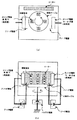
さらに、上記の被覆超硬工具が、例えば図2に概略説明図で示される物理蒸着装置の1種であるアークイオンプレーティング装置に上記の超硬基体を装入し、ヒータで装置内を、例えば500℃の温度に加熱した状態で、アノード電極と所定組成を有するTi−Si合金がセットされたカソード電極(蒸発源)との間に、例えば電圧:35V、電流:90Aの条件でアーク放電を発生させ、同時に装置内に反応ガスとして窒素ガスを導入して、例えば2Paの反応雰囲気とし、一方上記超硬基体には、例えば−100Vのバイアス電圧を印加した条件で、前記超硬合金基体の表面に、上記(Ti,Si)N層からなる硬質被覆層を蒸着することにより製造されることも知られている。
【0005】
【発明が解決しようとする課題】
近年の切削加工装置の高性能化はめざましく、一方で切削加工に対する省力化および省エネ化、さらに低コスト化の要求は強く、これに伴い、切削加工は高速化し、かつ切削条件は高切り込みや高送りなどの重切削化の傾向にあるが、上記の従来被覆超硬工具においては、これを通常の切削加工条件で用いた場合には問題はないが、断続切削加工を高い熱的機械的衝撃を伴う高切り込みや高送りなどの重切削条件で、かつ高速で行なった場合には、特に硬質被覆層の強度および靭性不足が原因でチッピング(微小割れ)が発生し易くなり、比較的短時間で使用寿命に至るのが現状である。
【0006】
【課題を解決するための手段】
そこで、本発明者等は、上述のような観点から、特に高速断続重切削加工で硬質被覆層がすぐれた耐チッピング性を発揮する被覆超硬工具を開発すべく、上記の従来被覆超硬工具を構成する硬質被覆層に着目し、研究を行った結果、
(a)上記の図2に示されるアークイオンプレーティング装置を用いて形成された従来被覆超硬工具を構成する(Ti,Si)N層は、層厚全体に亘って実質的に均一な組成を有し、したがって均質な高温硬さと耐熱性を有するが、例えば図1(a)に概略平面図で、同(b)に概略正面図で示される構造のアークイオンプレーティング装置、すなわち装置中央部に超硬基体装着用回転テーブルを設け、前記回転テーブルを挟んで、一方側にSi成分を含有したTi−Si合金、他方側に金属Tiをいずれもカソード電極(蒸発源)として対向配置したアークイオンプレーティング装置を用い、この装置の前記回転テーブルの外周部に沿って複数の超硬基体をリング状に装着し、この状態で装置内雰囲気を窒素雰囲気として前記回転テーブルを回転させると共に、蒸着形成される硬質被覆層の層厚均一化を図る目的で超硬基体自体も自転させながら、前記の両側のカソード電極(蒸発源)とアノード電極との間にアーク放電を発生させて、前記超硬基体の表面に(Ti,Si)N層を形成すると、この結果の(Ti,Si)N層においては、回転テーブル上にリング状に配置された前記超硬基体が上記の一方側のTi−Si合金のカソード電極(蒸発源)に最も接近した時点で層中にSi成分最高含有点が形成され、また前記超硬基体が上記の他方側の金属Tiのカソード電極に最も接近した時点で層中にTiN点(Si成分不含有点)が形成され、上記回転テーブルの回転によって層中には層厚方向にそって前記Si成分最高含有点とSi成分不含有点が所定間隔をもって交互に繰り返し現れると共に、前記Si成分最高含有点から前記Si成分不含有点、前記Si最低含有点から前記Si成分不含有点へSi成分含有量が連続的に変化する成分濃度分布構造をもつようになること。
【0007】
(b)上記(a)の繰り返し連続変化成分濃度分布構造の(Ti,Si)N層において、対向配置の一方側のカソード電極(蒸発源)であるTi−Si合金におけるSi成分含有量を上記の従来Ti−Si合金のSi成分含有量に相当するものとする共に、超硬基体が装着されている回転テーブルの回転速度を制御して、
上記Si成分最高含有点が、組成式:(Ti1-X SiX )N(ただし、原子比で、Xは0.20〜0.50を示す)、
を満足し、かつ隣り合う上記Si成分最高含有点とSi成分不含有点の厚さ方向の間隔を0.01〜0.1μmとすると、
上記Si成分最高含有点部分では、上記の従来(Ti,Si)N層のもつ高温硬さと耐熱性に相当するすぐれた高温硬さと耐熱性(高温特性)を示し、一方上記Si成分不含有点部分では、実質的にTiN点を中心にしてSi成分含有量の著しく低いものとなるので、TiNのもつ高強度と高靭性が確保され、かつこれらSi成分最高含有点とSi成分不含有点の間隔をきわめて小さくしたことから、層全体の特性としてすぐれた高温特性を保持した状態で一段とすぐれた強度と靭性を具備するようになり、したがって、硬質被覆層がかかる構成の(Ti,Si)N層からなる被覆超硬工具は、特に各種の鋼や鋳鉄などの断続切削加工を、高い熱的機械的衝撃を伴う高切り込みや高送りなどの重切削条件で、かつ高速で行なった場合にも、硬質被覆層がすぐれた耐チッピング性を発揮するようになること。
以上(a)および(b)に示される研究結果を得たのである。
【0008】
この発明は、上記の研究結果に基づいてなされたものであって、超硬基体の表面に、(Ti,Si)N層からなる硬質被覆層を1〜15μmの全体平均層厚で物理蒸着してなる被覆超硬工具において、
上記硬質被覆層が、層厚方向にそって、Si成分最高含有点(Ti成分最低含有点)とSi成分不含有点(TiN点)とが所定間隔をおいて交互に繰り返し存在し、かつ前記Si成分最高含有点から前記Si成分不含有点、前記Si成分不含有点から前記Si成分最高含有点へSi成分含有量が連続的に変化する成分濃度分布構造を有し、
さらに、上記Si成分最高含有点が、組成式:(Ti1-X SiX )N(ただし、原子比で、Xは0.20〜0.50を示す)、
を満足し、かつ隣り合う上記Si成分最高含有点とSi成分不含有点の間隔が、0.01〜0.1μmである、
高速断続重切削加工で硬質被覆層がすぐれた耐チッピング性を発揮する被覆超硬工具に特徴を有するものである。
【0009】
つぎに、この発明の被覆超硬工具において、これを構成する硬質被覆層の構成を上記の通りに限定した理由を説明する。
(a)Si成分最高含有点の組成
(Ti,Si)N層におけるSi成分は、高強度および高靭性を有するTiN層の高温硬さおよび耐熱性(高温特性)を向上させる目的で含有するものであり、したがってSi成分の含有割合が高くなればなるほど高温特性は向上したものになるが、その割合(X値)がTiとの合量に占める割合(原子比)で0.50を越えて高くなると、高強度および高靭性を有するTiN点が隣接して存在しても層自体の強度および靭性の低下は避けられず、この結果チッピングなどが発生し易くなり、一方その割合(X値)が同0.20未満では前記高温特性に所望の向上効果が得られないことから、その割合を0.20〜0.50と定めた。
【0010】
(b)Si成分最高含有点とSi成分不含有点間の間隔
その間隔が0.01μm未満ではそれぞれの点を上記の組成で明確に形成することが困難であり、この結果層に所望の高温特性と強度および靭性を確保することができなくなり、またその間隔が0.1μmを越えるとそれぞれの点もつ欠点、すなわちSi成分最高含有点であれば強度および靭性不足、Si不含有点であれば高温特性不足が層内に局部的に現れ、これが原因でチッピングが発生し易くなったり、摩耗進行が促進されるようになることから、その間隔を0.01〜0.1μmと定めた。
【0011】
(d)硬質被覆層の全体平均層厚
その層厚が1μm未満では、所望の耐摩耗性を確保することができず、一方その平均層厚が15μmを越えると、チッピングが発生し易くなることから、その平均層厚を1〜15μmと定めた。
【0012】
【発明の実施の形態】
つぎに、この発明の被覆超硬工具を実施例により具体的に説明する。
(実施例1)
原料粉末として、いずれも1〜3μmの平均粒径を有するWC粉末、TiC粉末、VC粉末、TaC粉末、NbC粉末、Cr3 C2 粉末、およびCo粉末を用意し、これら原料粉末を、表1に示される配合組成に配合し、ボールミルで72時間湿式混合し、乾燥した後、100MPa の圧力で圧粉体にプレス成形し、この圧粉体を6Paの真空中、温度:1400℃に1時間保持の条件で焼結し、焼結後、切刃部分にR:0.03のホーニング加工を施してISO規格・CNMG120408のチップ形状をもったWC基超硬合金製の超硬基体A1〜A10を形成した。
【0013】
また、原料粉末として、いずれも0.5〜2μmの平均粒径を有するTiCN(重量比でTiC/TiN=50/50)粉末、Mo2 C粉末、ZrC粉末、NbC粉末、TaC粉末、WC粉末、Co粉末、およびNi粉末を用意し、これら原料粉末を、表2に示される配合組成に配合し、ボールミルで24時間湿式混合し、乾燥した後、100MPaの圧力で圧粉体にプレス成形し、この圧粉体を2kPaの窒素雰囲気中、温度:1500℃に1時間保持の条件で焼結し、焼結後、切刃部分にR:0.03のホーニング加工を施してISO規格・CNMG120408のチップ形状をもったTiCN系サーメット製の超硬基体B1〜B6を形成した。
【0014】
ついで、上記の超硬基体A1〜A10およびB1〜B6のそれぞれを、アセトン中で超音波洗浄し、乾燥した状態で、図1に示されるアークイオンプレーティング装置内の回転テーブル上に外周部にそって装着し、一方側のカソード電極(蒸発源)として、種々の成分組成をもったSi成分最高含有点形成用Ti−Si合金、他方側のカソード電極(蒸発源)としてSi成分不含有点形成用金属Tiを前記回転テーブルを挟んで対向配置し、まず、装置内を排気して0.5Paの真空に保持しながら、ヒーターで装置内を500℃に加熱した後、Arガスを装置内に導入して10PaのAr雰囲気とし、前記回転テーブル上で自転しながら回転する超硬基体に−1000Vの直流バイアス電圧を印加して、超硬基体表面をArガスボンバート洗浄し、ついで装置内に反応ガスとして窒素ガスを導入して2Paの反応雰囲気とすると共に、前記回転テーブル上で自転しながら回転する超硬基体に−100Vの直流バイアス電圧を印加して、それぞれのカソード電極(前記Si成分最高含有点形成用Ti−Si合金およびSi成分不含有点形成用金属Ti)とアノード電極との間にアーク放電を発生させ、もって前記超硬基体の表面に、層厚方向に沿って表3,4に示される目標組成のSi成分最高含有点とSi成分不含有点(TiN点)とが交互に同じく表3,4に示される目標間隔で繰り返し存在し、かつ前記Si成分最高含有点から前記Si成分不含有点、前記Si成分不含有点から前記Si成分最高含有点へSi成分含有量が連続的に変化する成分濃度分布構造を有し、かつ同じく表3,4に示される目標全体層厚の硬質被覆層を蒸着することにより、図3(a)に概略斜視図で、同(b)に概略縦断面図で示される形状を有する本発明被覆超硬工具としての本発明表面被覆超硬合金製スローアウエイチップ(以下、本発明被覆超硬チップと云う)1〜16をそれぞれ製造した。
【0015】
また、比較の目的で、これら超硬基体A1〜A10およびB1〜B6を、アセトン中で超音波洗浄し、乾燥した状態で、それぞれ図2に示される通常のアークイオンプレーティング装置に装入し、一方カソード電極(蒸発源)として種々の成分組成をもったTi−Si合金を装着し、装置内を排気して0.5Paの真空に保持しながら、ヒーターで装置内を500℃に加熱した後、Arガスを装置内に導入して10PaのAr雰囲気とし、この状態で超硬基体に−1000Vのバイアス電圧を印加して超硬基体表面をArガスボンバート洗浄し、ついで装置内に反応ガスとして窒素ガスを導入して2Paの反応雰囲気とすると共に、前記超硬基体に印加するバイアス電圧を−100Vに下げて、前記カソード電極とアノード電極との間にアーク放電を発生させ、もって前記超硬基体A1〜A10およびB1〜B6のそれぞれの表面に、表5,6に示される目標組成および目標層厚を有し、かつ層厚方向に沿って実質的に組成変化のない(Ti,Si)N層からなる硬質被覆層を蒸着することにより、同じく図3に示される形状の従来被覆超硬工具としての従来表面被覆超硬合金製スローアウエイチップ(以下、従来被覆超硬チップと云う)1〜16をそれぞれ製造した。
【0016】
つぎに、上記本発明被覆超硬チップ1〜16および従来被覆超硬チップ1〜16について、これを工具鋼製バイトの先端部に固定治具にてネジ止めした状態で、
被削材:JIS・SCM440の長さ方向等間隔4本縦溝入り丸棒、
切削速度:400m/min.、
切り込み:5mm、
送り:0.3mm/rev.、
切削時間:5分、
の条件での合金鋼の乾式高速断続高切り込み切削加工試験、
被削材:JIS・S45Cの長さ方向等間隔4本縦溝入り丸棒、
切削速度:350m/min.、
切り込み:2.5mm、
送り:0.5mm/rev.、
切削時間:10分、
の条件での炭素鋼の乾式高速断続高送り切削加工試験、さらに、
被削材:JIS・FC300の長さ方向等間隔4本縦溝入り丸棒、
切削速度:350m/min.、
切り込み:5mm、
送り:0.35mm/rev.、
切削時間:5分、
の条件での鋳鉄の乾式高速断続高切り込み切削加工試験を行い、いずれの切削加工試験でも切刃の逃げ面摩耗幅を測定した。この測定結果を表3〜6に示した。
【0017】
【表1】

【表2】
【表3】
【表4】
【表5】
【表6】
(実施例2)
原料粉末として、平均粒径:5.5μmを有する中粗粒WC粉末、同0.8μmの微粒WC粉末、同1.3μmのTaC粉末、同1.2μmのNbC粉末、同1.2μmのZrC粉末、同2.3μmのCr3C2粉末、同1.5μmのVC粉末、同1.0μmの(Ti,W)C粉末、および同1.8μmのCo粉末を用意し、これら原料粉末をそれぞれ表7に示される配合組成に配合し、さらにワックスを加えてアセトン中で24時間ボールミル混合し、減圧乾燥した後、100MPaの圧力で所定形状の各種の圧粉体にプレス成形し、これらの圧粉体を、6Paの真空雰囲気中、7℃/分の昇温速度で1370〜1470℃の範囲内の所定の温度に昇温し、この温度に1時間保持後、炉冷の条件で焼結して、直径が8mm、13mm、および26mmの3種の超硬基体形成用丸棒焼結体を形成し、さらに前記の3種の丸棒焼結体から、研削加工にて、表7に示される組合せで、切刃部の直径×長さがそれぞれ6mm×13mm、10mm×22mm、および20mm×45mmの寸法をもった超硬基体(エンドミル)C−1〜C−8をそれぞれ製造した。
【0024】
ついで、これらの超硬基体(エンドミル)C−1〜C−8の表面に、ホーニングを施し、アセトン中で超音波洗浄し、乾燥した状態で、同じく図1に示されるアークイオンプレーティング装置に装入し、上記実施例1と同一の条件で、層厚方向に沿って表8に示される目標組成のSi成分最高含有点とSi成分不含有点とが交互に同じく表8に示される目標間隔で繰り返し存在し、かつ前記Si成分最高含有点から前記Si成分不含有点、前記Si成分不含有点から前記Si成分最高含有点へSi成分含有量が連続的に変化する成分濃度分布構造を有し、かつ同じく表8に示される目標全体層厚の硬質被覆層を蒸着することにより、図4(a)に概略正面図で、同(b)に切刃部の概略横断面図で示される形状を有する本発明被覆超硬工具としての本発明表面被覆超硬合金製エンドミル(以下、本発明被覆超硬エンドミルと云う)1〜8をそれぞれ製造した。
【0025】
また、比較の目的で、上記の超硬基体(エンドミル)C−1〜C−8の表面に、ホーニングを施し、アセトン中で超音波洗浄し、乾燥した状態で、同じく図2に示される通常のアークイオンプレーティング装置に装入し、上記実施例1と同一の条件で、表9に示される目標組成および目標層厚を有し、かつ層厚方向に沿って実質的に組成変化のない(Ti,Si)N層からなる硬質被覆層を蒸着することにより、従来被覆超硬工具としての従来表面被覆超硬合金製エンドミル(以下、従来被覆超硬エンドミルと云う)1〜8をそれぞれ製造した。
【0026】
つぎに、上記本発明被覆超硬エンドミル1〜8および従来被覆超硬エンドミル1〜8のうち、本発明被覆超硬エンドミル1〜3および従来被覆超硬エンドミル1〜3については、
被削材:平面寸法:100mm×250mm、厚さ:50mmのJIS・SKD11(硬さ:HB210)の板材、
切削速度:120m/min.、
溝深さ(切り込み):6mm、
テーブル送り:500mm/分、
の条件での工具鋼の湿式高速高切り込み溝切削加工試験、本発明被覆超硬エンドミル4〜6および従来被覆超硬エンドミル4〜6については、
被削材:平面寸法:100mm×250mm、厚さ:50mmのJIS・SUS304の板材、
切削速度:140m/min.、
溝深さ(切り込み):10mm、
テーブル送り:380mm/分、
の条件でのステンレス鋼の湿式高速高切り込み溝切削加工試験、本発明被覆超硬エンドミル7,8および従来被覆超硬エンドミル7,8については、
被削材:平面寸法:100mm×250mm、厚さ:50mmのJIS・SNCM439の板材、
切削速度:200m/min.、
溝深さ(切り込み):10mm、
テーブル送り:900mm/分、
の条件での合金鋼の湿式高速高送り溝切削加工試験(いずれの試験も水溶性切削油使用)、
をそれぞれ行い、いずれの溝切削加工試験でも切刃部先端面の直径が使用寿命の目安とされる0.2mm減少するまでの切削溝長を測定した。この測定結果を表8、9にそれぞれ示した。
【0027】
【表7】
【表8】
【表9】
(実施例3)
上記の実施例2で製造した直径が8mm(超硬基体C−1〜C−3形成用)、13mm(超硬基体C−4〜C−6形成用)、および26mm(超硬基体C−7、C−8形成用)の3種の丸棒焼結体を用い、この3種の丸棒焼結体から、研削加工にて、溝形成部の直径×長さがそれぞれ4mm×13mm(超硬基体D−1〜D−3)、8mm×22mm(超硬基体D−4〜D−6)、および16mm×45mm(超硬基体D−7、D−8)の寸法をもった超硬基体(ドリル)D−1〜D−8をそれぞれ製造した。
【0031】
ついで、これらの超硬基体(ドリル)D−1〜D−8の表面に、ホーニングを施し、アセトン中で超音波洗浄し、乾燥した状態で、同じく図1に示されるアークイオンプレーティング装置に装入し、上記実施例1と同一の条件で、層厚方向に沿って表10に示される目標組成のSi成分最高含有点とSi成分不含有点とが交互に同じく表10に示される目標間隔で繰り返し存在し、かつ前記Si成分最高含有点から前記Si成分不含有点、前記Si成分不含有点から前記Si成分最高含有点へSi成分含有量が連続的に変化する成分濃度分布構造を有し、かつ同じく表10に示される目標全体層厚の硬質被覆層を蒸着することにより、図5(a)に概略正面図で、同(b)に溝形成部の概略横断面図で示される形状を有する本発明被覆超硬工具としての本発明表面被覆超硬合金製ドリル(以下、本発明被覆超硬ドリルと云う)1〜8をそれぞれ製造した。
【0032】
また、比較の目的で、上記の超硬基体(ドリル)D−1〜D−8の表面に、ホーニングを施し、アセトン中で超音波洗浄し、乾燥した状態で、同じく図2に示される通常のアークイオンプレーティング装置に装入し、上記実施例1と同一の条件で、表11に示される目標組成および目標層厚を有し、かつ層厚方向に沿って実質的に組成変化のない(Ti,Si)N層からなる硬質被覆層を蒸着することにより、従来被覆超硬工具としての従来表面被覆超硬合金製エンドミル(以下、従来被覆超硬エンドミルと云う)1〜8をそれぞれ製造した。
【0033】
つぎに、上記本発明被覆超硬ドリル1〜8および従来被覆超硬ドリル1〜8のうち、本発明被覆超硬ドリル1〜3および従来被覆超硬ドリル1〜3については、
被削材:平面寸法:100mm×250厚さ:12mmのJIS・SKD61(硬さ:HRC52)の板材、
切削速度:60m/min.、
送り:0.20mm/rev、
の条件での工具鋼の湿式高速高送り穴あけ切削加工試験、本発明被覆超硬ドリル4〜6および従来被覆超硬ドリル4〜6については、
被削材:平面寸法:100mm×250mm、厚さ:24mmのJIS・FCD400の板材、
切削速度:80m/min.、
送り:0.35mm/rev、
の条件でのダクタイル鋳鉄の湿式高速高送り穴あけ切削加工試験、本発明被覆超硬ドリル7,8および従来被覆超硬ドリル7,8については、
被削材:平面寸法:100mm×250mm、厚さ:50mmのJIS・FC300の板材、
切削速度:90m/min.、
送り:0.45mm/rev、
の条件での鋳鉄の湿式高速高送り穴あけ切削加工試験、をそれぞれ行い、いずれの湿式高速穴あけ切削加工試験(水溶性切削油使用)でも先端切刃面の逃げ面摩耗幅が0.3mmに至るまでの穴あけ加工数を測定した。この測定結果を表10、11にそれぞれ示した。
【0034】
【表10】
【表11】
この結果得られた本発明被覆超硬工具としての本発明被覆超硬チップ1〜16、本発明被覆超硬エンドミル1〜8、および本発明被覆超硬ドリル1〜8を構成する硬質被覆層におけるSi成分最高含有点とSi成分不含有点の組成、並びに従来被覆超硬工具としての従来被覆超硬チップ1〜16、従来被覆超硬エンドミル1〜8、および従来被覆超硬ドリル1〜8の硬質被覆層の組成をオージェ分光分析装置を用いて測定したところ、それぞれ目標組成と実質的に同じ組成を示した。
なお、上記の本発明被覆超硬工具を構成する硬質被覆層において、Si成分最高含有点のSi含有割合が高い場合に、同Si成分不含有点に5原子%以下の割合でSiの含有が見られる場合があった。
また、これらの本発明被覆超硬工具の硬質被覆層におけるSi成分最高含有点とSi成分不含有点間の間隔、およびこれの全体層厚、並びに従来被覆超硬工具の硬質被覆層の厚さを、透過型電子顕微鏡を用いて断面測定したところ、いずれも目標値と実質的に同じ値を示した。
【0037】
【発明の効果】
表3〜11に示される結果から、硬質被覆層が層厚方向に、すぐれた高温硬さと耐熱性を有するSi成分最高含有点と高強度と高靭性を有するSi成分不含有点とが交互に所定間隔をおいて繰り返し存在し、かつ前記Si成分最高含有点から前記Si成分不含有点、前記Si成分不含有点から前記Si成分最高含有点へSi成分含有量が連続的に変化する成分濃度分布構造を有する本発明被覆超硬工具は、いずれも各種の鋼や鋳鉄などの断続切削加工を、高い熱的機械的衝撃を伴う高切り込みや高送りなどの重切削条件で、かつ高速で行なった場合にも、硬質被覆層がすぐれた耐チッピング性を発揮するのに対して、硬質被覆層が層厚方向に沿って実質的に組成変化のない(Ti,Si)N層からなる従来被覆超硬工具においては、前記硬質被覆層がすぐれた高温硬さと耐熱性を有するものの、強度および靭性に劣るものであるために、チッピングが発生し、これが原因で比較的短時間で使用寿命に至ることが明らかである。
上述のように、この発明の被覆超硬工具は、通常の条件での切削加工は勿論のこと、特に各種の鋼や鋳鉄などの断続切削加工を、高い熱的機械的衝撃を伴う高切り込みや高送りなどの重切削条件で、かつ高速で行なった場合にも、すぐれた耐チッピング性を発揮し、長期に亘ってすぐれた耐摩耗性を示すものであるから、切削加工装置の高性能化、並びに切削加工の省力化および省エネ化、さらに低コスト化に十分満足に対応できるものである。
【図面の簡単な説明】
【図1】この発明の被覆超硬工具を構成する硬質被覆層を形成するのに用いたアークイオンプレーティング装置を示し、(a)は概略平面図、(b)は概略正面図である。
【図2】従来被覆超硬工具を構成する硬質被覆層を形成するのに用いた通常のアークイオンプレーティング装置の概略説明図である。
【図3】(a)は被覆超硬チップの概略斜視図、(b)は被覆超硬チップの概略縦断面図である。
【図4】(a)は被覆超硬エンドミル概略正面図、(b)は同切刃部の概略横断面図である。
【図5】(a)は被覆超硬ドリルの概略正面図、(b)は同溝形成部の概略横断面図である。[0001]
BACKGROUND OF THE INVENTION
In this invention, the hard coating layer has high strength and high toughness, and is excellent in high temperature hardness and heat resistance. Therefore, particularly in intermittent cutting of various steels and cast irons, high thermal mechanical impact is required. Related to surface-coated cemented carbide cutting tools (hereinafter referred to as coated carbide tools) that exhibit excellent chipping resistance with a hard coating layer when performed at high speed under heavy cutting conditions such as cutting and high feed It is.
[0002]
[Prior art]
In general, coated carbide tools have a throw-away tip and cutting blade that are used by attaching to the tip of the cutting tool for turning and planing of various steels and cast irons. There are drills and miniature drills that are used for drilling and cutting, and also solid type end mills that are used for surface cutting, grooving, shoulder processing, etc. that also take the form of intermittent cutting. There is known a slow-away end mill tool that can be freely mounted and cut in the same manner as the solid type end mill.
[0003]
Further, as a coated carbide tool, a substrate made of tungsten carbide (hereinafter referred to as WC) -based cemented carbide or titanium carbonitride (hereinafter referred to as TiCN) -based cermet (hereinafter collectively referred to as a cemented carbide substrate). ), A composite nitride of Ti and Si satisfying the composition formula: (Ti 1-X Si X ) N (wherein X is 0.20 to 0.50 in atomic ratio) [hereinafter, ( Coated carbide tools formed by physically vapor-depositing hard coating layers consisting of [Ti, Si) N] layers with an average layer thickness of 1 to 15 μm have been proposed, for continuous cutting and intermittent cutting of various steels and cast iron Has been tried to put to practical use.
[0004]
Furthermore, the above-mentioned coated carbide tool is, for example, the above-mentioned carbide substrate is inserted into an arc ion plating apparatus which is one type of physical vapor deposition apparatus schematically shown in FIG. For example, arc discharge between the anode electrode and the cathode electrode (evaporation source) on which a Ti—Si alloy having a predetermined composition is set in a state heated to a temperature of 500 ° C., for example, under conditions of voltage: 35 V and current: 90 A At the same time, nitrogen gas is introduced into the apparatus as a reaction gas to form a reaction atmosphere of, for example, 2 Pa. On the other hand, the cemented carbide substrate is subjected to, for example, a bias voltage of −100 V, for example. It is also known that it is produced by vapor-depositing a hard coating layer composed of the above (Ti, Si) N layer on the surface.
[0005]
[Problems to be solved by the invention]
In recent years, the performance of cutting machines has improved dramatically, while there has been a strong demand for labor-saving and energy-saving and low-cost cutting, which has led to cutting speeds and cutting conditions with high cutting depth and high cutting conditions. Although there is a tendency for heavy cutting such as feeding, there is no problem when using the above conventional coated carbide tools under normal cutting conditions, but intermittent cutting is highly thermal mechanical shock. When it is performed at high speeds and under heavy cutting conditions such as high depth of cut and high feed with high hardness, chipping (microcracking) is likely to occur, especially due to insufficient strength and toughness of the hard coating layer. At present, the service life is reached.
[0006]
[Means for Solving the Problems]
In view of the above, the present inventors have developed the above-mentioned conventional coated carbide tool in order to develop a coated carbide tool that exhibits excellent chipping resistance with a hard coating layer particularly excellent in high-speed intermittent heavy cutting. As a result of conducting research focusing on the hard coating layer that composes
(A) The (Ti, Si) N layer constituting the conventional coated carbide tool formed using the arc ion plating apparatus shown in FIG. 2 has a substantially uniform composition over the entire layer thickness. Therefore, for example, the arc ion plating apparatus having the structure shown in the schematic plan view of FIG. 1A and the schematic front view of FIG. A rotating table for mounting a carbide substrate is provided in the part, and a Ti-Si alloy containing Si component is placed on one side and metal Ti is placed on the other side as a cathode electrode (evaporation source) across the rotating table. Using an arc ion plating apparatus, a plurality of carbide substrates are mounted in a ring shape along the outer periphery of the rotary table of the apparatus, and in this state, the atmosphere in the apparatus is set to a nitrogen atmosphere to form the rotary table. Arc discharge is generated between the cathode electrode (evaporation source) and the anode electrode on both sides while rotating and rotating the carbide substrate itself for the purpose of uniforming the thickness of the hard coating layer to be deposited. When the (Ti, Si) N layer is formed on the surface of the cemented carbide substrate, the cemented carbide substrate arranged in a ring shape on the rotary table is the above-described (Ti, Si) N layer. When the Ti-Si alloy cathode electrode (evaporation source) closest to the Ti-Si alloy on one side is formed, a point containing the highest Si component is formed in the layer, and the carbide substrate becomes the cathode electrode of the metal Ti on the other side. At the closest point, TiN points (Si component-free points) are formed in the layer, and by rotation of the rotary table, the Si component highest content point and Si component-free points are formed in the layer along the layer thickness direction. Alternately at predetermined intervals It has a component concentration distribution structure in which the Si component content continuously changes from the Si component highest content point to the Si component non-contained point and from the Si lowest content point to the Si component non-contained point. To become a.
[0007]
(B) In the (Ti, Si) N layer having the repeated continuous change component concentration distribution structure of (a) above, the Si component content in the Ti—Si alloy which is the cathode electrode (evaporation source) on one side of the opposing arrangement is described above. And corresponding to the Si component content of the conventional Ti-Si alloy, and controlling the rotation speed of the turntable on which the carbide substrate is mounted,
The Si component highest content point is the composition formula: (Ti 1-X Si X ) N (wherein X is 0.20 to 0.50 in atomic ratio),
And the distance between the adjacent Si component highest content point and Si component non-contained point in the thickness direction is 0.01 to 0.1 μm,
The above Si component highest content point shows excellent high temperature hardness and heat resistance (high temperature characteristics) corresponding to the high temperature hardness and heat resistance of the conventional (Ti, Si) N layer, while the Si component non-contained point In the portion, since the Si component content is substantially low centering on the TiN point, the high strength and high toughness of TiN are ensured, and the highest Si component content point and the Si component non-contained point are secured. Since the distance is extremely small, the layer has a higher strength and toughness while maintaining excellent high-temperature characteristics as the characteristics of the entire layer. Therefore, (Ti, Si) N having a structure in which the hard coating layer is applied. Coated carbide tools consisting of layers, especially when intermittent cutting of various types of steel and cast iron is performed at high speed under heavy cutting conditions such as high cutting and high feed with high thermal mechanical impact. , Hard To become possible to exert chipping resistance of the coating layer is excellent.
The research results shown in (a) and (b) above were obtained.
[0008]
The present invention has been made based on the above research results. A hard coating layer composed of a (Ti, Si) N layer is physically vapor-deposited on the surface of a cemented carbide substrate with an overall average layer thickness of 1 to 15 μm. In the coated carbide tool
In the hard coating layer, the Si component highest content point (Ti component lowest content point) and the Si component non-content point (TiN point) are alternately present at predetermined intervals along the layer thickness direction, and A component concentration distribution structure in which the Si component content continuously changes from the Si component highest content point to the Si component non-content point, from the Si component non-content point to the Si component highest content point,
Further, the highest Si component content point is a composition formula: (Ti 1-X Si x ) N (wherein X is 0.20 to 0.50 in atomic ratio),
And the distance between the adjacent Si component highest content point and the Si component non-contained point is 0.01 to 0.1 μm,
This is characterized by a coated carbide tool that exhibits excellent chipping resistance with a hard coating layer in high-speed intermittent heavy cutting.
[0009]
Next, in the coated carbide tool of the present invention, the reason why the structure of the hard coating layer constituting the tool is limited as described above will be described.
(A) Composition with the highest Si component content point (Ti, Si) The Si component in the N layer is contained for the purpose of improving the high temperature hardness and heat resistance (high temperature characteristics) of the TiN layer having high strength and high toughness. Therefore, the higher the content ratio of the Si component, the higher the high temperature characteristics, but the ratio (X value) exceeds 0.50 in the ratio (atomic ratio) to the total amount with Ti. When it becomes high, even if TiN points having high strength and high toughness are present adjacent to each other, a decrease in the strength and toughness of the layer itself is inevitable, and as a result, chipping and the like are likely to occur, while the ratio (X value) However, if it is less than 0.20, the desired improvement effect cannot be obtained in the high temperature characteristics, so the ratio was set to 0.20 to 0.50.
[0010]
(B) Interval between Si component highest content point and Si component non-content point If the distance is less than 0.01 μm, it is difficult to clearly form each point with the above composition. It becomes impossible to secure the characteristics, strength and toughness, and when the distance exceeds 0.1 μm, each point has a defect, that is, if the Si component is the highest content point, the strength and toughness is insufficient, if the Si content is not included Insufficient high-temperature characteristics appear locally in the layer, which makes it easy for chipping to occur and promotes the progress of wear. Therefore, the interval was set to 0.01 to 0.1 μm.
[0011]
(D) Overall average layer thickness of hard coating layer If the layer thickness is less than 1 μm, desired wear resistance cannot be ensured. On the other hand, if the average layer thickness exceeds 15 μm, chipping tends to occur. Therefore, the average layer thickness was determined to be 1 to 15 μm.
[0012]
DETAILED DESCRIPTION OF THE INVENTION
Next, the coated carbide tool of the present invention will be specifically described with reference to examples.
Example 1
As raw material powders, WC powder, TiC powder, VC powder, TaC powder, NbC powder, Cr 3 C 2 powder, and Co powder, all having an average particle diameter of 1 to 3 μm, were prepared. And then wet-mixed with a ball mill for 72 hours, dried, and press-molded into a green compact at a pressure of 100 MPa. The green compact was vacuumed at 6 Pa at a temperature of 1400 ° C. for 1 hour. Sintered under the holding conditions, and after sintering, the cutting edge portion was subjected to a honing process of R: 0.03, and the carbide bases A1 to A10 made of WC-based cemented carbide having ISO / CNMG120408 chip shape Formed.
[0013]
In addition, as raw material powders, all are TiCN (weight ratio TiC / TiN = 50/50) powder, Mo 2 C powder, ZrC powder, NbC powder, TaC powder, WC powder having an average particle diameter of 0.5 to 2 μm. Co powder and Ni powder are prepared, and these raw material powders are blended in the blending composition shown in Table 2, wet mixed by a ball mill for 24 hours, dried, and then pressed into a compact at a pressure of 100 MPa. The green compact was sintered in a nitrogen atmosphere of 2 kPa at a temperature of 1500 ° C. for 1 hour, and after sintering, the cutting edge portion was subjected to a honing process of R: 0.03 to obtain ISO standard / CNMG120408. TiCN-based cermet carbide substrates B1 to B6 having the following chip shape were formed.
[0014]
Next, each of the above-mentioned carbide substrates A1 to A10 and B1 to B6 is ultrasonically cleaned in acetone and dried, on the rotary table in the arc ion plating apparatus shown in FIG. Therefore, as one cathode electrode (evaporation source), a Ti-Si alloy for forming the highest Si component point with various component compositions, and as the other cathode electrode (evaporation source), no Si component-containing point The forming metal Ti is disposed opposite to the rotary table, and first, the interior of the apparatus is heated to 500 ° C. with a heater while evacuating the apparatus and maintaining a vacuum of 0.5 Pa, and then Ar gas is introduced into the apparatus. Is introduced into a 10 Pa Ar atmosphere, a DC bias voltage of −1000 V is applied to the carbide substrate rotating while rotating on the rotary table, and the surface of the carbide substrate is subjected to Ar gas bombardment. Next, nitrogen gas is introduced into the apparatus as a reaction gas to form a reaction atmosphere of 2 Pa, and a DC bias voltage of −100 V is applied to a carbide substrate that rotates while rotating on the rotary table. Arc discharge was generated between the cathode electrode (Ti-Si alloy for forming Si component highest content point and metal Ti for not forming Si component point) and the anode electrode, and a layer was formed on the surface of the carbide substrate. Along with the thickness direction, the Si component highest content point and Si component non-contained point (TiN point) of the target composition shown in Tables 3 and 4 are alternately present at the target intervals shown in Tables 3 and 4, and Having a component concentration distribution structure in which the Si component content continuously changes from the Si component highest content point to the Si component non-content point, from the Si component non-content point to the Si component highest content point, and By depositing a hard coating layer having a target total layer thickness shown in Tables 3 and 4, the coating of the present invention having a shape shown in a schematic perspective view in FIG. 3A and a schematic longitudinal sectional view in FIG. The present invention surface-coated cemented carbide throwaway tips (hereinafter referred to as the present invention coated carbide tips) 1 to 16 as carbide tools were produced, respectively.
[0015]
Further, for the purpose of comparison, these carbide substrates A1 to A10 and B1 to B6 are ultrasonically cleaned in acetone and dried, and then loaded into a normal arc ion plating apparatus shown in FIG. On the other hand, Ti—Si alloys having various component compositions were attached as cathode electrodes (evaporation sources), and the inside of the apparatus was heated to 500 ° C. with a heater while the inside of the apparatus was evacuated and maintained at a vacuum of 0.5 Pa. Thereafter, Ar gas is introduced into the apparatus to form an Ar atmosphere of 10 Pa. In this state, a bias voltage of −1000 V is applied to the cemented carbide substrate to clean the surface of the cemented carbide substrate with Ar gas bombardment, and then the reaction gas is introduced into the device. Nitrogen gas is introduced to form a reaction atmosphere of 2 Pa, and the bias voltage applied to the cemented carbide substrate is lowered to −100 V so that an arc is provided between the cathode electrode and the anode electrode. A discharge is generated, so that the surfaces of the cemented carbide substrates A1 to A10 and B1 to B6 have the target compositions and target layer thicknesses shown in Tables 5 and 6, and substantially along the layer thickness direction. By depositing a hard coating layer composed of a (Ti, Si) N layer having no composition change, a conventional surface-coated cemented carbide throwaway tip (hereinafter, referred to as a conventional coated carbide tool having the shape shown in FIG. 3). 1 to 16 were manufactured.
[0016]
Next, with the present invention coated carbide tips 1-16 and conventional coated carbide tips 1-16, in a state where this is screwed to the tip of the tool steel tool with a fixing jig,
Work material: JIS · SCM440 lengthwise equidistant 4 vertical grooved round bar,
Cutting speed: 400 m / min. ,
Cutting depth: 5mm,
Feed: 0.3 mm / rev. ,
Cutting time: 5 minutes
Dry high-speed intermittent high-cut cutting test of alloy steel under the conditions
Work material: JIS · S45C lengthwise equal 4 round grooved round bars,
Cutting speed: 350 m / min. ,
Incision: 2.5mm,
Feed: 0.5 mm / rev. ,
Cutting time: 10 minutes,
Carbon steel dry high-speed intermittent high-feed cutting test,
Work material: JIS / FC300 lengthwise equidistant 4 bars with vertical grooves,
Cutting speed: 350 m / min. ,
Cutting depth: 5mm,
Feed: 0.35 mm / rev. ,
Cutting time: 5 minutes
The dry high-speed intermittent high-cut cutting test of cast iron was performed under the conditions described above, and the flank wear width of the cutting edge was measured in any cutting test. The measurement results are shown in Tables 3-6.
[0017]
[Table 1]
[Table 2]
[Table 3]
[Table 4]
[Table 5]
[Table 6]
(Example 2)
As raw material powders, medium coarse WC powder having an average particle diameter of 5.5 μm, fine WC powder of 0.8 μm, TaC powder of 1.3 μm, NbC powder of 1.2 μm, ZrC of 1.2 μm Prepare a powder, 2.3 μm Cr 3 C 2 powder, 1.5 μm VC powder, 1.0 μm (Ti, W) C powder, and 1.8 μm Co powder. Each was blended in the blending composition shown in Table 7, further added with wax, ball milled in acetone for 24 hours, dried under reduced pressure, then pressed into various compacts of a predetermined shape at a pressure of 100 MPa. The green compact is heated to a predetermined temperature in the range of 1370 to 1470 ° C. at a rate of temperature increase of 7 ° C./min in a 6 Pa vacuum atmosphere, held at this temperature for 1 hour, and then fired under furnace cooling conditions. Finally, the diameters are 8mm, 13mm, and 26 3 types of sintered carbide rod forming bodies for forming a carbide substrate of m, and further, the diameter of the cutting edge portion by the combination shown in Table 7 by grinding from the above three types of sintered rods. X Carbide substrates (end mills) C-1 to C-8 having lengths of 6 mm x 13 mm, 10 mm x 22 mm, and 20 mm x 45 mm, respectively, were produced.
[0024]
Next, honing is performed on the surfaces of these carbide substrates (end mills) C-1 to C-8, ultrasonic cleaning is performed in acetone, and the surface is dried, and the arc ion plating apparatus shown in FIG. In the same conditions as in Example 1 above, the Si component highest content point and Si component non-contained point of the target composition shown in Table 8 along the layer thickness direction are alternately shown in Table 8 A component concentration distribution structure that repeatedly exists at intervals, and in which the Si component content continuously changes from the Si component highest content point to the Si component non-content point, and from the Si component non-content point to the Si component highest content point. And by depositing a hard coating layer having a target total layer thickness also shown in Table 8, it is shown in a schematic front view in FIG. 4 (a) and in a schematic cross-sectional view of the cutting edge part in FIG. 4 (b). Coated carbide tool of the present invention having a shape The present invention surface coating cemented carbide end mill of Te (hereinafter, the present invention refers to the coating end mills) 1-8 were prepared, respectively.
[0025]
Further, for comparison purposes, the surfaces of the above-mentioned carbide substrates (end mills) C-1 to C-8 are honed, ultrasonically cleaned in acetone, and dried. And having the target composition and target layer thickness shown in Table 9 under the same conditions as in Example 1 and substantially no composition change along the layer thickness direction. By vapor-depositing a hard coating layer composed of a (Ti, Si) N layer, conventional surface-coated cemented carbide end mills (hereinafter referred to as conventional coated carbide end mills) 1 to 8 are manufactured as conventional coated carbide tools, respectively. did.
[0026]
Next, of the present invention coated carbide end mills 1-8 and conventional coated carbide end mills 1-8, the present invention coated carbide end mills 1-3 and conventional coated carbide end mills 1-3 are as follows:
Work material: Plane dimension: 100 mm × 250 mm, thickness: 50 mm JIS / SKD11 (hardness: HB210) plate material,
Cutting speed: 120 m / min. ,
Groove depth (cut): 6 mm
Table feed: 500 mm / min,
With respect to the tool steel wet high-speed high-cut groove cutting test, the coated carbide end mills 4 to 6 and the conventional coated carbide end mills 4 to 6 of the present invention,
Work material: Plane dimension: 100 mm × 250 mm, thickness: 50 mm JIS / SUS304 plate,
Cutting speed: 140 m / min. ,
Groove depth (cut): 10 mm,
Table feed: 380 mm / min,
For stainless steel wet high-speed high-grooving groove cutting test, coated carbide end mills 7 and 8 of the present invention and conventional coated carbide end mills 7 and 8
Work material: Plane dimension: 100 mm × 250 mm, thickness: 50 mm JIS / SNCM439 plate material,
Cutting speed: 200 m / min. ,
Groove depth (cut): 10 mm,
Table feed: 900 mm / min,
Wet high-speed high-feed grooving cutting test of alloy steel under the conditions of (All tests use water-soluble cutting oil),
In each of the groove cutting tests, the cutting groove length was measured until the diameter of the tip surface of the cutting edge decreased by 0.2 mm, which is a guide for the service life. The measurement results are shown in Tables 8 and 9, respectively.
[0027]
[Table 7]
[Table 8]
[Table 9]
(Example 3)
The diameters produced in Example 2 above were 8 mm (for forming carbide substrates C-1 to C-3), 13 mm (for forming carbide substrates C-4 to C-6), and 26 mm (for carbide substrates C-). 7, for C-8 formation), from these three types of round bar sintered bodies, the diameter x length of the groove forming portion is 4 mm x 13 mm (by grinding), respectively. Carbide substrates D-1 to D-3), 8 mm × 22 mm (Carbide substrates D-4 to D-6), and 16 mm × 45 mm (Carbide substrates D-7, D-8) Hard substrates (drills) D-1 to D-8 were produced, respectively.
[0031]
Next, honing is performed on the surfaces of these carbide substrates (drills) D-1 to D-8, ultrasonic cleaning is performed in acetone, and the surface is dried, and the arc ion plating apparatus shown in FIG. In the same conditions as in Example 1 above, the Si component highest content point and Si component non-contained point of the target composition shown in Table 10 along the layer thickness direction are also shown in Table 10 alternately. A component concentration distribution structure that repeatedly exists at intervals, and in which the Si component content continuously changes from the Si component highest content point to the Si component non-content point, and from the Si component non-content point to the Si component highest content point. By depositing a hard coating layer having a target total layer thickness shown in Table 10 as well, a schematic front view is shown in FIG. 5 (a), and a schematic cross-sectional view of the groove forming portion is shown in FIG. 5 (b). Carbide coated carbide of the present invention having a shape The present invention surface coating cemented carbide drill as (hereinafter, the present invention refers to the coating carbide drills) 1-8 were prepared, respectively.
[0032]
For comparison purposes, the surfaces of the above-mentioned carbide substrates (drills) D-1 to D-8 are subjected to honing, ultrasonically cleaned in acetone, and dried, as shown in FIG. And having the target composition and target layer thickness shown in Table 11 and substantially no composition change along the layer thickness direction under the same conditions as in Example 1 above. By vapor-depositing a hard coating layer composed of a (Ti, Si) N layer, conventional surface-coated cemented carbide end mills (hereinafter referred to as conventional coated carbide end mills) 1 to 8 are manufactured as conventional coated carbide tools, respectively. did.
[0033]
Next, of the present invention coated carbide drills 1-8 and conventional coated carbide drills 1-8, the present invention coated carbide drills 1-3 and conventional coated carbide drills 1-3,
Work material: Plane dimension: 100 mm x 250 Thickness: 12 mm JIS / SKD61 (hardness: HRC52) plate material,
Cutting speed: 60 m / min. ,
Feed: 0.20mm / rev,
With respect to the tool steel wet high-speed high-feed drilling test, the present invention coated carbide drills 4-6 and the conventional coated carbide drills 4-6,
Work material: Plane dimension: 100 mm × 250 mm, thickness: 24 mm JIS / FCD400 plate material,
Cutting speed: 80 m / min. ,
Feed: 0.35mm / rev,
For the ductile cast iron wet high-speed high-feed drilling test under the conditions of the present invention, the coated carbide drills 7 and 8 of the present invention and the conventional coated carbide drills 7 and 8,
Work material: Plane dimensions: 100 mm x 250 mm, thickness: 50 mm JIS / FC300 plate material,
Cutting speed: 90 m / min. ,
Feed: 0.45mm / rev,
Wet high-speed high-feed drilling machining test of cast iron under the conditions of each, and in any wet high-speed drilling machining test (using water-soluble cutting oil), the flank wear width of the cutting edge surface reaches 0.3 mm The number of drilling processes up to was measured. The measurement results are shown in Tables 10 and 11, respectively.
[0034]
[Table 10]
[Table 11]
In the hard coating layer which comprises this invention coated carbide tip 1-16 as this invention coated carbide tool obtained as a result, this invention coated carbide end mill 1-8, and this invention coated carbide drill 1-8. Composition of Si component highest content point and Si component non-content point, and conventionally coated carbide tips 1 to 16 as conventional coated carbide tools, conventionally coated carbide end mills 1 to 8, and conventionally coated carbide drills 1 to 8 When the composition of the hard coating layer was measured using an Auger spectroscopic analyzer, the composition was substantially the same as the target composition.
In addition, in the hard coating layer constituting the above-described coated carbide tool of the present invention, when the Si content ratio of the Si component highest content point is high, the Si content is not included in the Si component non-contained point and the content of Si is 5 atomic% or less. It was sometimes seen.
In addition, the distance between the Si component highest content point and the Si component non-contained point in the hard coating layer of these coated carbide tools of the present invention, the total layer thickness thereof, and the thickness of the hard coating layer of the conventional coated carbide tool When cross sections were measured using a transmission electron microscope, all showed substantially the same value as the target value.
[0037]
【The invention's effect】
From the results shown in Tables 3 to 11, the hard coating layer alternates in the layer thickness direction with the Si component highest content point having excellent high-temperature hardness and heat resistance and the Si component-free point having high strength and high toughness. Component concentration that repeatedly exists at predetermined intervals, and in which the Si component content continuously changes from the Si component highest content point to the Si component non-content point, and from the Si component non-content point to the Si component highest content point The coated carbide tool of the present invention having a distributed structure performs intermittent cutting of various steels and cast irons at high speed under heavy cutting conditions such as high cutting and high feed with high thermal mechanical impact. In this case, the hard coating layer exhibits excellent chipping resistance, whereas the hard coating layer is a conventional coating composed of a (Ti, Si) N layer having substantially no composition change along the layer thickness direction. For carbide tools, the hard Although covering layer has excellent high-temperature hardness and heat resistance, because it is inferior in strength and toughness, chipping occurs and this is apparent that lead to a relatively short time service life due.
As described above, the coated cemented carbide tool of the present invention can be used not only for cutting under normal conditions, but also for intermittent cutting such as various steels and cast irons. High cutting performance due to excellent chipping resistance and excellent wear resistance over a long period even under heavy cutting conditions such as high feed and at high speeds In addition, it is possible to sufficiently satisfy the labor saving and energy saving of the cutting process and the cost reduction.
[Brief description of the drawings]
FIG. 1 shows an arc ion plating apparatus used for forming a hard coating layer constituting a coated carbide tool of the present invention, wherein (a) is a schematic plan view and (b) is a schematic front view.
FIG. 2 is a schematic explanatory view of a normal arc ion plating apparatus used to form a hard coating layer constituting a conventional coated carbide tool.
FIG. 3A is a schematic perspective view of a coated carbide chip, and FIG. 3B is a schematic longitudinal sectional view of the coated carbide chip.
4A is a schematic front view of a coated carbide end mill, and FIG. 4B is a schematic cross-sectional view of the cutting edge portion.
5A is a schematic front view of a coated carbide drill, and FIG. 5B is a schematic cross-sectional view of the groove forming portion.
Claims (1)
さらに、上記Si成分最高含有点が、組成式:(Ti1-X SiX )N(ただし、原子比で、Xは0.20〜0.50を示す)、
を満足し、かつ隣り合う上記Si成分最高含有点とSi成分不含有点の間隔が、0.01〜0.1μmであること、
を特徴とする高速断続重切削加工で硬質被覆層がすぐれた耐チッピング性を発揮する表面被覆超硬合金製切削工具。Surface-coated carbide formed by physical vapor deposition of a hard coating layer composed of a composite nitride layer of Ti and Si on the surface of a tungsten carbide-based cemented carbide substrate or a titanium carbonitride-based cermet substrate with an overall average layer thickness of 1 to 15 μm. In the alloy cutting tool, the hard coating layer has a Si component highest content point (Ti component lowest content point) and a Si component non-content point (TiN point) alternately at predetermined intervals along the layer thickness direction. It has a component concentration distribution structure that repeatedly exists and the Si component content continuously changes from the Si component highest content point to the Si component non-content point and from the Si component non-content point to the Si component highest content point. ,
Further, the highest Si component content point is a composition formula: (Ti 1-X Si x ) N (wherein X is 0.20 to 0.50 in atomic ratio),
And the distance between the adjacent Si component highest content point and the Si component non-contained point is 0.01 to 0.1 μm,
A surface-coated cemented carbide cutting tool that exhibits excellent chipping resistance in high-speed intermittent heavy-cutting, characterized by its high hardness.
Priority Applications (1)
| Application Number | Priority Date | Filing Date | Title |
|---|---|---|---|
| JP2002034140A JP3951292B2 (en) | 2002-02-12 | 2002-02-12 | Cutting tool made of surface-coated cemented carbide that provides excellent chipping resistance with a hard coating layer in high-speed intermittent machining |
Applications Claiming Priority (1)
| Application Number | Priority Date | Filing Date | Title |
|---|---|---|---|
| JP2002034140A JP3951292B2 (en) | 2002-02-12 | 2002-02-12 | Cutting tool made of surface-coated cemented carbide that provides excellent chipping resistance with a hard coating layer in high-speed intermittent machining |
Publications (2)
| Publication Number | Publication Date |
|---|---|
| JP2003231004A JP2003231004A (en) | 2003-08-19 |
| JP3951292B2 true JP3951292B2 (en) | 2007-08-01 |
Family
ID=27776731
Family Applications (1)
| Application Number | Title | Priority Date | Filing Date |
|---|---|---|---|
| JP2002034140A Expired - Fee Related JP3951292B2 (en) | 2002-02-12 | 2002-02-12 | Cutting tool made of surface-coated cemented carbide that provides excellent chipping resistance with a hard coating layer in high-speed intermittent machining |
Country Status (1)
| Country | Link |
|---|---|
| JP (1) | JP3951292B2 (en) |
Families Citing this family (1)
| Publication number | Priority date | Publication date | Assignee | Title |
|---|---|---|---|---|
| JP3996809B2 (en) | 2002-07-11 | 2007-10-24 | 住友電工ハードメタル株式会社 | Coated cutting tool |
Family Cites Families (5)
| Publication number | Priority date | Publication date | Assignee | Title |
|---|---|---|---|---|
| EP0496053B1 (en) * | 1991-01-21 | 1995-07-26 | Balzers Aktiengesellschaft | Coated highly wear-resistant tool and physical coating method for highly wear-resistant tools |
| JP3416938B2 (en) * | 1994-10-28 | 2003-06-16 | 住友電気工業株式会社 | Laminate |
| JP3572728B2 (en) * | 1995-06-23 | 2004-10-06 | 三菱マテリアル株式会社 | Hard layer coated cutting tool |
| JP3382781B2 (en) * | 1996-06-05 | 2003-03-04 | 日立ツール株式会社 | Multi-layer coated hard tool |
| JP3347687B2 (en) * | 1999-05-19 | 2002-11-20 | 日立ツール株式会社 | Hard coating tool |
-
2002
- 2002-02-12 JP JP2002034140A patent/JP3951292B2/en not_active Expired - Fee Related
Also Published As
| Publication number | Publication date |
|---|---|
| JP2003231004A (en) | 2003-08-19 |
Similar Documents
| Publication | Publication Date | Title |
|---|---|---|
| JP3969230B2 (en) | Surface coated cemented carbide cutting tool with excellent chipping resistance with hard coating layer under heavy cutting conditions | |
| JP3669334B2 (en) | Surface-coated cemented carbide cutting tool with excellent wear resistance due to high-speed cutting and hard coating layer | |
| JP2002239810A (en) | Surface covered cemented carbide made cutting tool excellent in surface lubricity against chip | |
| JP3928480B2 (en) | Surface coated cemented carbide cutting tool with excellent wear resistance with hard coating layer in high speed cutting | |
| JP2003326403A (en) | Cutting tool made of surface coated cemented carbide providing excellent wear resistance by hard layer in high speed heavy cutting | |
| JP3844285B2 (en) | Surface-coated cemented carbide cutting tool with excellent wear resistance due to high-speed cutting and hard coating layer | |
| JP4389152B2 (en) | Surface-coated cemented carbide cutting tool that exhibits excellent chipping resistance under heavy cutting conditions. | |
| JP3695396B2 (en) | Surface-coated cemented carbide cutting tool with excellent wear resistance in high-speed cutting of difficult-to-cut materials | |
| JP4375527B2 (en) | Cutting tool made of surface-coated cemented carbide that exhibits excellent chipping resistance under high-speed heavy cutting conditions. | |
| JP4007102B2 (en) | Surface coated cemented carbide cutting tool with excellent chipping resistance with hard coating layer under high speed heavy cutting conditions | |
| JP3985227B2 (en) | Surface coated cemented carbide cutting tool with excellent chipping resistance with hard coating layer under high speed heavy cutting conditions | |
| JP3982301B2 (en) | Surface coated cemented carbide cutting tool with excellent chipping resistance with hard coating layer under high speed heavy cutting conditions | |
| JP2003136302A (en) | Surface coated cemented carbide cutting tool having hard coating layer exerting excellent wear resistance in high-speed cutting | |
| JP3951292B2 (en) | Cutting tool made of surface-coated cemented carbide that provides excellent chipping resistance with a hard coating layer in high-speed intermittent machining | |
| JP3928461B2 (en) | Surface-coated cemented carbide cutting tool with excellent wear resistance under high-speed heavy cutting conditions. | |
| JP3962910B2 (en) | Surface coated cemented carbide cutting tool with excellent chipping resistance due to hard coating layer in heavy cutting | |
| JP3944900B2 (en) | Surface coated cemented carbide cutting tool with excellent wear resistance with hard coating layer in high speed cutting | |
| JP4366987B2 (en) | Cutting tool made of surface-coated cemented carbide that exhibits excellent chipping resistance under high-speed heavy cutting conditions. | |
| JP3928487B2 (en) | Surface coated cemented carbide cutting tool with excellent wear resistance with hard coating layer in high speed cutting | |
| JP3928459B2 (en) | Cutting tool made of surface-coated cemented carbide that provides excellent wear resistance with a hard coating layer in high-speed cutting of difficult-to-cut materials | |
| JP3928452B2 (en) | Surface coated cemented carbide cutting tool with excellent chipping resistance with hard coating layer under heavy cutting conditions | |
| JP3944901B2 (en) | Cutting tool made of surface-coated cemented carbide that exhibits excellent chipping resistance with a hard coating layer in intermittent heavy cutting | |
| JP3928434B2 (en) | Cutting tool made of surface-coated cemented carbide that exhibits excellent chipping resistance with a hard coating layer in intermittent heavy cutting | |
| JP2004344990A (en) | Cutting tool of surface-coated cemented carbide with hard coating layer achieving excellent abrasion resistance in high speed heavy cutting condition, and method for manufacturing the same | |
| JP3962913B2 (en) | A method of forming a hard coating layer on the cutting tool surface that exhibits excellent wear resistance in high-speed cutting |
Legal Events
| Date | Code | Title | Description |
|---|---|---|---|
| A621 | Written request for application examination |
Free format text: JAPANESE INTERMEDIATE CODE: A621 Effective date: 20050125 |
|
| A977 | Report on retrieval |
Free format text: JAPANESE INTERMEDIATE CODE: A971007 Effective date: 20061110 |
|
| TRDD | Decision of grant or rejection written | ||
| A01 | Written decision to grant a patent or to grant a registration (utility model) |
Free format text: JAPANESE INTERMEDIATE CODE: A01 Effective date: 20070402 |
|
| A61 | First payment of annual fees (during grant procedure) |
Free format text: JAPANESE INTERMEDIATE CODE: A61 Effective date: 20070415 |
|
| R150 | Certificate of patent or registration of utility model |
Free format text: JAPANESE INTERMEDIATE CODE: R150 |
|
| FPAY | Renewal fee payment (event date is renewal date of database) |
Free format text: PAYMENT UNTIL: 20100511 Year of fee payment: 3 |
|
| S111 | Request for change of ownership or part of ownership |
Free format text: JAPANESE INTERMEDIATE CODE: R313115 |
|
| FPAY | Renewal fee payment (event date is renewal date of database) |
Free format text: PAYMENT UNTIL: 20100511 Year of fee payment: 3 |
|
| R360 | Written notification for declining of transfer of rights |
Free format text: JAPANESE INTERMEDIATE CODE: R360 |
|
| FPAY | Renewal fee payment (event date is renewal date of database) |
Free format text: PAYMENT UNTIL: 20100511 Year of fee payment: 3 |
|
| R360 | Written notification for declining of transfer of rights |
Free format text: JAPANESE INTERMEDIATE CODE: R360 |
|
| R371 | Transfer withdrawn |
Free format text: JAPANESE INTERMEDIATE CODE: R371 |
|
| S111 | Request for change of ownership or part of ownership |
Free format text: JAPANESE INTERMEDIATE CODE: R313115 |
|
| FPAY | Renewal fee payment (event date is renewal date of database) |
Free format text: PAYMENT UNTIL: 20100511 Year of fee payment: 3 |
|
| R350 | Written notification of registration of transfer |
Free format text: JAPANESE INTERMEDIATE CODE: R350 |
|
| FPAY | Renewal fee payment (event date is renewal date of database) |
Free format text: PAYMENT UNTIL: 20100511 Year of fee payment: 3 |
|
| S531 | Written request for registration of change of domicile |
Free format text: JAPANESE INTERMEDIATE CODE: R313531 |
|
| FPAY | Renewal fee payment (event date is renewal date of database) |
Free format text: PAYMENT UNTIL: 20100511 Year of fee payment: 3 |
|
| R350 | Written notification of registration of transfer |
Free format text: JAPANESE INTERMEDIATE CODE: R350 |
|
| FPAY | Renewal fee payment (event date is renewal date of database) |
Free format text: PAYMENT UNTIL: 20100511 Year of fee payment: 3 |
|
| FPAY | Renewal fee payment (event date is renewal date of database) |
Free format text: PAYMENT UNTIL: 20110511 Year of fee payment: 4 |
|
| FPAY | Renewal fee payment (event date is renewal date of database) |
Free format text: PAYMENT UNTIL: 20110511 Year of fee payment: 4 |
|
| FPAY | Renewal fee payment (event date is renewal date of database) |
Free format text: PAYMENT UNTIL: 20120511 Year of fee payment: 5 |
|
| FPAY | Renewal fee payment (event date is renewal date of database) |
Free format text: PAYMENT UNTIL: 20120511 Year of fee payment: 5 |
|
| FPAY | Renewal fee payment (event date is renewal date of database) |
Free format text: PAYMENT UNTIL: 20130511 Year of fee payment: 6 |
|
| FPAY | Renewal fee payment (event date is renewal date of database) |
Free format text: PAYMENT UNTIL: 20130511 Year of fee payment: 6 |
|
| LAPS | Cancellation because of no payment of annual fees |