JP3929116B2 - Memory subsystem - Google Patents
Memory subsystem Download PDFInfo
- Publication number
- JP3929116B2 JP3929116B2 JP17996997A JP17996997A JP3929116B2 JP 3929116 B2 JP3929116 B2 JP 3929116B2 JP 17996997 A JP17996997 A JP 17996997A JP 17996997 A JP17996997 A JP 17996997A JP 3929116 B2 JP3929116 B2 JP 3929116B2
- Authority
- JP
- Japan
- Prior art keywords
- clock
- data
- controller
- memory
- signal line
- Prior art date
- Legal status (The legal status is an assumption and is not a legal conclusion. Google has not performed a legal analysis and makes no representation as to the accuracy of the status listed.)
- Expired - Fee Related
Links
Images


Classifications
-
- G—PHYSICS
- G06—COMPUTING; CALCULATING OR COUNTING
- G06F—ELECTRIC DIGITAL DATA PROCESSING
- G06F13/00—Interconnection of, or transfer of information or other signals between, memories, input/output devices or central processing units
- G06F13/14—Handling requests for interconnection or transfer
- G06F13/16—Handling requests for interconnection or transfer for access to memory bus
-
- G—PHYSICS
- G06—COMPUTING; CALCULATING OR COUNTING
- G06F—ELECTRIC DIGITAL DATA PROCESSING
- G06F13/00—Interconnection of, or transfer of information or other signals between, memories, input/output devices or central processing units
- G06F13/38—Information transfer, e.g. on bus
- G06F13/42—Bus transfer protocol, e.g. handshake; Synchronisation
- G06F13/4204—Bus transfer protocol, e.g. handshake; Synchronisation on a parallel bus
- G06F13/4234—Bus transfer protocol, e.g. handshake; Synchronisation on a parallel bus being a memory bus
- G06F13/4243—Bus transfer protocol, e.g. handshake; Synchronisation on a parallel bus being a memory bus with synchronous protocol
Description
【0001】
【発明の属する技術分野】
本発明は、クロックに同期して動作するメモリ又はそのようなメモリを複数個搭載して大容量のメモリとして機能するメモリモジュールを使用して構成するメモリサブシステムに関し、特に簡単な機構で高速のデータ転送が可能なメモリサブシステムに関する。
【0002】
【従来の技術】
半導体装置を使用したコンピュータ等の大規模な半導体装置システムでは、システムの各部分がクロックに同期して動作するように構成されており、データ信号やアドレス信号等の信号の入出力はクロック信号に同期して行われる。図1は、SDRAMなどのクロックに同期して動作するメモリを使用して構成したメモリサブシステムの従来の構成例を示す図である。図示のように、コントローラ12からは、コマンド信号が印加される制御信号バス14、アドレス信号が印加されるアドレス信号バス15、及びデータ信号が印加されるデータ信号バス16が延びており、これらの配線に沿ってメモリ13−1、13−2、…、13−mが配置され、各メモリはこれらの配線に接続される。クロック発生回路10はシステムを構成する各要素に供給するクロックを発生させる回路で、クロック発生回路10で発生されたクロックはクロック分配回路11を介して、コントローラ12、及びメモリ13−1、13−2、…、13−mに供給される。近年、複数のメモリ素子を搭載し、大容量で高速のアクセスが可能なメモリとして機能するDIMM(Dual Inline Memory Module)が使用されているが、これをメモリ13−1、13−2、…、13−mの代わりに使用することも可能である。
【0003】
図1のクロック分配システム11は、分配されたクロックがすべて同一の位相になるように、クロック発生回路10からコントローラ12、及びメモリ13−1、13−2、…、13−mに至る配線長及び負荷が等しい等長配線回路である。
図2は、説明を容易にするため、図1のシステムにおいてメモリが1個とした場合の構成、及びコントローラ12とメモリ13の内部の構成を示す図であり、ここでは2つの構成例が示されている。なお、以下の説明では、データ信号の最小変化周期はクロックの半周期であり、クロックの立ち上がりエッジと立ち下がりエッジの両方のエッジに同期してデータが変化するダブルデータレート(DDR)方式のSDRAMを使用する場合の例を説明することとする。従って、データ信号の入力回路は、データ信号の変化から最小変化周期の1/2、すなわちクロックの1/4周期(90°)ずれたタイミングでデータ信号を取り込むのが最適なタイミングであるとする。また、データ信号以外のコマンド信号やアドレス信号の最小変化周期はデータ信号の最小変化周期より長いため、これらの信号の取込みのタイミングはあまり問題にならない。そこで、これらの信号の伝送については従来と同じ構成が使用されるので、ここでは説明を省略するものとする。更に、説明を容易にするため、データ信号バスを、コントローラ12からメモリ13に書き込む書込データを伝送する書込データバス16aと、メモリ13からコントローラ12に送る読出データを伝送する読出データバス16bとに分けて示すが、書込データと読出データを同一のデータバスで伝送することも可能である。
【0004】
図2の(1)の構成例では、メモリ13にデータを書き込む場合には、コントローラ12は、シフトクロック発生回路21でクロック発生回路10の供給するクロックCLKから1/4周期ずれたシフトクロックを発生させ、メモリ13に書き込む書込データDinをデータ出力回路22からシフトクロックに同期して書込データバス16aに出力する。メモリ13は、データ入力回路32でこの書込データDinをクロックCLKに同期して取り込む。メモリ13からデータを読み出す場合には、メモリ13は、シフトクロック発生回路31でクロック発生回路10の供給するクロックCLKから1/4周期ずれたシフトクロックを発生させ、内部回路34で発生された読出データDoutを、データ出力回路33からシフトクロックに同期して読出データバス16bに出力する。コントローラ12は、データ入力回路23でこの読出データDoutをクロックに同期して取り込む。
【0005】
図3は、図2の(1)に示した構成例におけるデータの入出力動作を示すタイムチャートである。(a)を付したDinとDoutはコントローラ12側のデータであることを、(b)を付したDinとDoutはメモリ13側のデータであることを示す。これは以下の図でも同じである。図示のように、コントローラ12から出力された書込データDin(a)は、クロックCLKの変化エッジから1/4周期ずれた時点で変化している。すなわち、クロックCLKの変化エッジが、書込データDin(a)の最適な取込みタイミングに位置している。書込データDin(a)は、メモリ13までの距離に対応する伝搬時間を経過してメモリ13に到達し、書込データDin(b)となる。メモリ13に供給されるクロックCLKは、コントローラ12に供給されるクロックCLKと同一位相であるから、データ入力回路32は最適なタイミングから上記の伝搬時間分ずれたタイミングで書込データDinを取り込むことになる。
【0006】
逆に、メモリ13からデータを読み出す時には、コントローラ12からメモリ13にクロックCLKの立ち上がりエッジに同期してアドレス信号などの信号が伝送され、それに応じてメモリ13で必要な処理を行って、アクセス時間tAC後から読出データDout(b)がデータ出力回路33から読出データバス16bに出力される。読出データDout(b)は上記の伝搬時間分遅れてコントローラ12に到達し、Dout(a)になる。コントローラ12は、クロックCLKの次の立ち上がりエッジに同期してデータ入力回路23で読出データDoutを取り込む。
【0007】
図2の(1)に示した構成では、メモリ13側はクロックCLKを使用して書込データを取込み、コントローラ12側は次のクロックの立ち上がりエッジを使用して読出データを取り込めばよく、構成が非常に簡単であるが、クロック周波数が十分に小さい場合には、伝搬時間は無視でき、十分な余裕をもって伝送されたデータを取り込むことができ、何ら問題は生じなかった。
【0008】
図2の(1)のシステムでは、データ信号を出力する送信側がデータ信号の出力タイミングをずらすことにより、受信側ではクロックのエッジに同期してデータ信号を取り込めるようにしたが、各種の変形が可能である。例えば、図2の(2)は、送信はクロックのエッジに同期して行い、受信はクロックのエッジからずれたタイミングで行うようにした構成例である。図2の(2)の構成においてデータを書き込む時には、コントローラ12はクロックCLKに同期してデータ出力回路22から書込データを出力し、メモリはこの書込データをデータ入力回路32で、シフトクロック発生回路31で発生されたずれたクロックに同期して取込む。データを読み出す時には、メモリ13はクロックCLKに同期してデータ出力回路33から読出データを出力し、コントローラ12は、シフトクロック発生回路31で発生されたずれたクロックに同期して、この読出データをデータ入力回路23で取り込む。更に、コントローラ12が書込データの出力と読出データの取込みをずれたシフトクロックに同期して行うようにすれば、メモリ13は書込データの取込みと読出データの出力を共にクロックCLKに同期して行うことができ、シフトクロック発生回路はコントローラ12にのみ設ければよい。いずれにしろ、コントローラ12とメモリ13の一方又は両方にそれぞれシフトクロック発生回路が必要である。
【0009】
上記のように、クロック周波数が小さい場合には、信号のばらつきによるシフトクロック発生回路21の精度の低下もほとんど問題にならず、単純な回路構成でも問題は生じなかった。しかし、クロック周波数が大きくなると、伝搬時間のクロック周期に対する割合が大きくなり、信号の伝搬時間による取込みタイミングのずれが問題になってくる。また、シフトクロック発生回路におけるプロセスばらつきや温度の変動によるシフトクロックのずれが問題になってくる。
【0010】
このような問題を解決する高速動作のためのシステム構成がいくつか提案されており、図4はそのようなシステムの構成例を示す図である。図4のシステムは、基本クロックCLKとは別にデータストローブ信号DQSを用いて、データの送信を行う方式を使用しており、書込データDinと読出データDoutの送信の両方でデータストローブ信号DQSを使用する双方向方式(バイディレクショナル方式)と呼ばれる方式を使用する。コントローラ12は、クロックCLKから1/4周期ずれた2つのシフトクロックを発生するシフトクロック発生回路21と、書込データDinを一方のシフトクロックCLKに同期して出力するデータ出力回路22と、他方のシフトクロックを出力するストローブ信号出力回路24と、メモリ13から送信されたストローブ信号を受信するストローブ信号入力回路25と、ストローブ信号入力回路25の受信したストローブ信号に同期してメモリ13から送信された読出データDoutを取り込むデータ入力回路23とを有する。また、メモリ13は、コントローラ12から送信されたストローブ信号を受信するストローブ信号入力回路35と、書込データDinをストローブ信号に同期して取り込むデータ入力回路32と、クロックCLK及び内部回路34で発生する読出データDoutが出力できる状態になったことを示す信号から、1/4周期ずれた2つのシフトクロックを発生するシフトクロック発生回路31と、読出データDoutを一方のシフトクロックCLKに同期して出力するデータ出力回路33と、他方のシフトクロックを出力するストローブ信号出力回路36とを有する。書込データを伝送する書込データバス16aと、読出データを伝送する読出データバス16bと、ストローブ信号を伝送するストローブ信号線17は、同じ伝搬時間になるように並行に等長配線されている。
【0011】
図5は図4のシステムにおける書込データの伝送動作を示すタイムチャートである。書込データの伝送する時、コントローラ12はデータ出力回路22から書込データDin(a)を、ストローブ信号出力回路24からデータストローブ信号DQS(a)を出力する。図5に示すように、書込データDin(a)とデータストローブ信号DQS(a)は、1/4周期ずれている。従って、データストローブ信号DQSの変化エッジは、書込データDinを取り込むのに最適なタイミングである。なお、データストローブ信号DQSとクロックCLKとの間には一定の位相関係はない。書込データDin(a)とデータストローブ信号DQS(a)がメモリ13に伝送されても、書込データバス16aとデータストローブ信号17は並行に設けられているため、ほとんどスキューは生ぜず、そのままの位相関係を維持される。従って、メモリ13における書込データDin(b)とデータストローブ信号DQS(b)は、書込データDin(a)とデータストローブ信号DQS(a)を伝送時間分送らせた信号である。そのため、メモリ13のデータ入力回路32でストローブ信号入力回路35で受信したストローブ信号に同期して書込データを取り込めば最適なタイミングで取り込むことができる。メモリ13に取り込まれた書込データの内部回路34への書込は、取り込んだ後のクロックCLKの立ち上がりエッジから開始される。
【0012】
図6は図4のシステムにおける読出データの伝送動作を示すタイムチャートである。読出データの伝送する時、メモリ13はデータ出力回路33から読出データDout(b)を、ストローブ信号出力回路36からデータストローブ信号DQS(b)を出力する。図6に示すように、読出データDout(b)とデータストローブ信号DQS(b)は、1/4周期ずれている。従って、データストローブ信号DQSの変化エッジは、読出データDoutを取り込むのに最適なタイミングである。なお、データストローブ信号DQSとクロックCLKとの間には一定の位相関係はない。読出データDout(b)とデータストローブ信号DQS(b)がコントローラ12に伝送されても、読出データ信号線16bとデータストローブ信号線17は並行に設けられているため、ほとんどスキューは生ぜず、そのままの位相関係を維持される。従って、コントローラ12における読出データDout(a)とデータストローブ信号DQS(a)は、読出データDout(b)とデータストローブ信号DQS(b)を伝送時間分送らせた信号である。そのため、コントローラ12のデータ入力回路23でストローブ信号入力回路25で受信したストローブ信号に同期して読出データを取り込めば最適なタイミングで取り込むことができる。コントローラ12に取り込まれた読出データのCPUでの処理は、取り込んだ後のクロックCLKの立ち上がりエッジから開始される。
【0013】
以上のように、図4の双方向ストローブ方式であれば、いずれの方向にデータを伝送する場合も、データと同じ方向に取込みに適したストローブ信号が出力されるので、常に最適なタイミングで送信データを取り込むことができる。但し、図2の回路と同様に、図4の回路は、コントローラ12とメモリ13にそれぞれ1/4位相ずれた2つのシフトクロックを発生させるためのシフトクロック発生回路を設ける必要がある。更に、ストローブ信号を伝送するためのストローブ信号線及びその入力回路と出力回路が必要である。
【0014】
図7は、高速動作のためのシステムの別の構成例を示す図である。このシステムは、メモリ13へはコントローラ12からクロックCLKを供給し、クロックCLKを供給するためのクロック信号線18を書込データバス16aに並行に設ける。そして、コントローラ12からメモリ13への書込データの伝送は、クロックCLKを1/4周期ずらした信号に同期して行う。メモリ13からコントローラ12への読出データの伝送は、図4のシステムと同様に、データストローブ信号DQSに同期して行い、一緒にメモリ13からコントローラ12へデータストローブ信号を伝送する。この方式は、一方のデータ信号(ここでは読出データ)の伝送にのみデータストローブ信号DQSを使用するため、片方向方式(ユニディレクショナル方式)と呼ばれる。コントローラ12は、受信したクロックCLKをクロック信号線18をに印加するクロック出力回路27と、クロックCLKから1/4周期ずれたシフトクロックを発生するシフトクロック発生回路21と、書込データDinをシフトクロックCLKに同期して出力するデータ出力回路22と、メモリ13から送信されたストローブ信号を受信するストローブ信号入力回路25と、ストローブ信号入力回路25の受信したストローブ信号から1/4周期ずれたシフトクロックを発生するシフトクロック発生回路26と、シフトクロック発生回路26の出力するシフトクロックに同期して、メモリ13から送信された読出データDoutを取り込むデータ入力回路23とを有する。また、メモリ13は、コントローラ12から送信されたクロック信号CLKを受信するクロック入力回路37と、書込データDinをクロック信号CLKに同期して取り込むデータ入力回路32と、読出データDoutをクロック入力回路37の出力するクロックCLKに同期して出力するデータ出力回路33と、クロック入力回路37の出力するクロックCLKをストローブ信号として出力するストローブ信号出力回路36とを有する。クロックCLKを伝送するクロック信号線18と、書込データを伝送する書込データバス16aと、読出データを伝送する読出データバス16bと、ストローブ信号を伝送するストローブ信号線17bは、同じ伝搬時間になるように並行に等長配線されている。
【0015】
図8は図7のシステムにおける書込データの伝送動作を示すタイムチャートである。コントローラ12はクロック出力回路27からクロックCLKを常時出力し、出力書込データの伝送する時には、データ出力回路22から書込データDin(a)を出力する。図8に示すように、書込データDin(a)とクロックCLKは、1/4周期ずれている。従って、クロックCLKの変化エッジは、書込データDinを取り込むのに最適なタイミングである。書込データDin(a)とクロックCLKがメモリ13に伝送されても、書込データ信号線16aとクロック信号線18は並行に設けられているため、ほとんどスキューは生ぜず、そのままの位相関係を維持される。従って、メモリ13における書込データDin(b)とクロックCLK(b)は、書込データDin(a)とクロックCLK(a)を伝送時間分送らせた信号である。そのため、メモリ13のデータ入力回路32でクロック入力回路37で受信したクロック信号CLKに同期して書込データを取り込めば最適なタイミングで取り込むことができる。
【0016】
図9は図7のシステムにおける読出データの伝送動作を示すタイムチャートである。読出データの伝送する時、メモリ13はデータ出力回路33から読出データDout(b)を、ストローブ信号出力回路36からデータストローブ信号DQS(b)を出力する。図9に示すように、書込データDout(b)とデータストローブ信号DQS(b)は、1/4周期ずれている。従って、データストローブ信号DQSの変化エッジは、書込データDoutを取り込むのに最適なタイミングである。書込データDout(b)とデータストローブ信号DQS(b)がコントローラ12に伝送されても、読出データ信号線16bとデータストローブ信号17は並行に設けられているため、ほとんどスキューは生ぜず、そのままの位相関係を維持される。従って、コントローラ12における読出データDout(a)とデータストローブ信号DQS(a)は、書込データDout(b)とデータストローブ信号DQS(b)を伝送時間分送らせた信号である。そのため、コントローラ12のデータ入力回路23でストローブ信号入力回路25で受信したストローブ信号に同期して書込データを取り込めば最適なタイミングで取り込むことができる。
【0017】
以上のように、図7の片方向ストローブ方式では、いずれの方向にデータを伝送する場合も、常に最適なタイミングで送信データを取り込むことができる。
以上、3つの従来例を説明したが、いずれの従来例においても、位相がデータ信号の最小変化周期の1/2ずれたシフトクロックを発生させることが必要である。具体的には、データ信号の最小変化周期がクロックの周期と同じであれば、クロックと正確に位相が一致した信号と1/2周期(180°)ずれた信号が必要である。データ信号の最小変化周期がクロックの1/2周期で、クロックの立ち上がりエッジと立ち下がりエッジの両方でデータ信号が変化するDDR−SDRAMの場合には、具体的には位相が0又は1周期(360°)、1/4周期(90°)、1/2周期(180°)、3/4周期(270°)のシフトクロックを発生させることが必要である。正確にこのような位相ずれた信号を発生させるためには、DLL(Delay Locked Loop) 回路が使用される。
【0018】
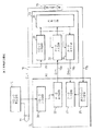
図10は、クロックCLKから等位相(0°)のシフトクロックと、1/4周期(90°)ずつずれたシフトクロックを発生させるDLL回路の基本構成を示す図である。図10において、参照番号41は0°位相のシフトクロックを発生させるDLL回路であり、51は90°ずつずれた4つのシフトクロックを発生させるDLL回路である。
【0019】
0°DLL回路41は、クロックCLKを遅延させ、遅延量が調整できるディレイ回路42と、ディレイ回路42の出力する遅延クロックとクロックCLKの位相を比較する位相比較回路43と、位相比較回路43の比較結果に基づいて2つのクロックの位相が一致するようにディレイ回路42での遅延量を段階的に変化させるディレイ制御回路44とを有する。ディレイ回路42の出力する遅延クロックとクロックCLKの位相が一致した時には、ディレイ回路42の出力する遅延クロックは、クロックCLKに対して1周期遅れた信号である。ディレイ回路42は微少な遅延量を有する遅延素子を多数直列に接続し、各段から出力が取り出せるようにスイッチを設けた回路で、どのスイッチを動作させてどの段から出力を得るかにより、遅延量が変化させられる。
【0020】
90°DLL回路51は、0°位相のシフトクロックを得るための0°DLL回路と同じ構成であるが、ディレイ回路を4分割して4個の1/4ディレイ回路52、53、54、55とし、前段の出力が後段の入力になるように直列に接続してある。ディレイ制御回路57は、4分割された各1/4ディレイ回路の遅延量が同一になるように同時に制御している。位相比較回路56は、最初の1/4ディレイ回路52に入力されるクロック信号φと最終の1/4ディレイ回路55から出力される信号の位相を比較する。ディレイ制御回路57は比較結果に基づいて2つの信号の位相が一致するように4つの1/4ディレイ回路の遅延量を制御する。2つの信号の位相が一致した時には、各1/4ディレイ回路の出力は1/4周期ずつずれている。このようにして、1/4周期ずつずれたシフトクロックが得られる。
【0021】
このように、DLL回路を使用することにより、正確に所定位相ずれた信号を得ることができるが、DLL回路は、かなり複雑で回路規模の大きな回路で、チップ面積も大きく、消費電力も大きい。
【0022】
【発明が解決しようとする課題】
以上説明した従来例では、いずれもコントローラ内部又はメモリ、又は両方に、例えば1/4周期位相のずれた信号を発生させるシフトクロック発生回路を設けて、適当なタイミングで送信データを取り込めるようにしており、正確に所定位相ずれた信号を発生させるためには、DLL回路を使用する必要がある。DDR−SDRAMの場合、立ち上がりエッジと立ち下がりエッジの両方を基準にしてデータを送信し、取り込む必要がある。
【0023】
供給されるクロックのデューティ比が正確に50%の場合は、そのままクロックの立ち上がりエッジと立ち下がりエッジを使用でき、クロックの立ち上がりエッジと立ち下がりエッジから1/4周期位相のずれた信号を発生させる。そこで図10に示した90°DLL回路51を使用することになる。
また、クロックのデューティ比が50%からずれている時には、まず1/2周期(180°)位相の異なる信号を発生させ、その後その信号から1/4周期位相のずれた信号を発生させることが考えられるが、この場合には2個のDLL回路が必要になる。このようなDLL回路を2回使用すると、ディレイ回路の最小変化量で決定されるDLLのジッタが2倍になり、シフトクロックの精度が悪化するという問題がある。
【0024】
そこで、やはり図10に示した90°DLL回路51を使用して、1/4周期(90°)ずれた信号と1/2周期(180°)ずれた信号を発生させる。しかし、図10に示した90°DLL回路51は、DLL回路が4段に接続されており、各DLL回路の最小変化量の4倍のジッタが発生するため、シフトクロックの精度が低くなるという問題がある。
【0025】
更に、DLL回路は、上記のように、複雑な回路であり、このような回路をコントローラ及びメモリに設けると、チップ面積が増大してコストアップになると共に、消費電力も増大するという問題を生じる。
本発明は、このような問題を解決するためのもので、高速のデータ送信が可能なメモリシステムを簡単な構成で実現することを目的とする。
【0026】
【課題を解決するための手段】
本発明のメモリサブシステムは、上記目的を実現するため、コントローラ又はメモリからデータを出力する場合には、クロック又はデータストローブ信号に同期してデータを出力し、データ信号線と並行に設けられたクロック信号線又はデータストローブ信号線でクロック又はデータストローブ信号を伝送するようにしたシステムにおいて、クロック信号線又はデータストローブ信号線に所定の遅延を生じる遅延回路を設けて、伝送先ではクロック又はデータストローブ信号はデータ信号に対して取り込みに適した位相になり、受信したクロック又はデータストローブ信号でそのままデータ信号を取り込めるようにする。このような構成であれば、DLL回路を使用しないで、上記の問題は生じない。また、DDR−SDRAMのように、クロックの立ち上がりエッジと立ち下がりエッジの両方を基準にしてデータを送信し、取り込む必要がある場合でも、180°位相の異なる信号を発生させる180°DLL回路のみを設ければよいので、ジッタの発生が低減される。
【0027】
すなわち、本発明のメモリサブシステムは、読出コマンドを出力する出力回路と、読出データを取り込む読出データ入力回路とを有するコントローラと、それぞれが前記読出コマンドを取り込むコマンド入力回路と、前記読出コマンドに応じて前記読出データを出力する読出データ出力回路とを有する複数のメモリと、前記コントローラと前記複数のメモリの間に接続されたクロック信号線又はデータストローブ信号線と、前記読出データを送るために前記コントローラと前記複数のメモリの間に接続されたデータ信号線とを備え、前記コントローラは、初期化動作時に、前記クロックのサイクル数を計数して、前記コントローラが前記読出コマンドを出力する時点から前記コントローラが前記メモリから前記読出データを取り込む時点までのアクセス時間として記憶し、前記コントローラが前記読出データを正規のタイミングで取り込むことを可能にし、前記メモリサブシステムは、前記コントローラと前記複数のメモリのうちの1つとの間又は前記メモリ間の、前記クロック信号線又は前記データストローブ信号線に配置された少なくとも1つの遅延回路をさらに備え、前記少なくとも1つの遅延回路の遅延量は、前記アクセス時間が前記クロックの前記サイクルの整数倍にほぼ等しい値から偏移するように決定されることを特徴とする。
【0028】
上記の所定の遅延は、クロック又はデータストローブ信号がデータ信号の取り込みに適した位相になる遅延であり、書込データ及び読出データの最小変化周期の1/2の時間であり、DDR−SDRAMの場合であれば、クロック周期の1/4の遅延である。
遅延回路は、信号線の信号伝搬時間を長くするように配線を長くした回路又はディレイ素子を使用したディレイラインで実現できる。
【0029】
クロック信号線とデータストローブ信号線は、インピーダンスが整合していることが望ましい。
遅延回路は、コントローラとメモリの間の部分に設けることが望ましいが、スペースの関係でコントローラとメモリの間に設けることができない場合には、コントローラとメモリの外側に設けることも可能である。
【0030】
クロック信号線へのクロックの印加は、コントローラ又はクロック源から行う。クロック源から行う時には、コントローラに供給するクロックを分岐するか、並行に行う。
データストローブ信号として、メモリが受信したクロックを使用してもよい。その場合、メモリは読出データを伝送する時には、受信したクロックの変化エッジで読出データを変化させ、データストローブ信号線はメモリの付近でクロック信号線に接続される。
【0031】
従来は、クロック又はデータストローブ信号が送信データに対して取り込みに適した位相になるようにするためのシフトクロック発生回路を、コントローラ及びメモリに設けていた。そのため、信号線を長くして位相を調整することができず、DLL回路を使用する必要があった。これに対して、本発明では、チップ外で位相調整するため、信号線を長くするなどの簡単な構成で位相調整が行える。
【0032】
【発明の実施の形態】
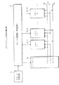
図11の(1)は、本発明の実施例のメモリサブシステムの全体構成を示す図である。図11の(1)に示すように、本実施例のメモリサブシステムは、クロック発生回路10からコントローラ12にクロックが供給され、コントローラ12からは、クロック信号線18、書込データバス16a、読出データバス16b、及びデータストローブ信号線17bが並行に延びている。クロック信号線18とデータストローブ信号線17bには、伝送する信号を所定時間遅延させるために信号線を延長した延長部71と72が設けられている。他にも、コマンド信号を伝送する制御信号バスやアドレス信号を伝送するアドレス信号バスが設けられているが、ここでは省略してある。上記の信号線にはソケット61が設けられており、このソケット61を介してDIMM−SDRAMと呼ばれるメモリモジュール60aから60cが接続されている。DIMM−SDRAMは、図11の(2)に示すように、複数のメモリ素子(ここではSDRAM)を有し、これらを合わせた大容量のメモリとして動作するように、デコーダ64やマルチプレクサ65aと65bなどを有し、外部との接続のための接続ピンが設けられている。この接続ピンがモジュールの両面で独立しているためDual Inline 型と呼ばれる。なお、このようなDIMM−SDRAMでなく、単に接続ピンに直接接続された複数のSDRAMを有するだけで、デコーダ64やマルチプレクサ65aと65bなどがないメモリモジュールでもよく、SDRAM単体でもよい。以下、説明を簡単にするために、単にメモリとして説明を行う。
1つのソケット61には、複数のメモリ(DIMM)が接続されて群を成している。各群内では信号の伝搬時間は無視できる程度の差であるとする。しかし、多数の群が接続されると信号線が長くなり、その伝搬時間の差が問題になる。後述するように、本実施例では、メモリの位置にかかわらず良好なタイミングで伝送データを取り込めるようにしているが、メモリの位置により、データの読み出し時にコントローラ12から各メモリにアクセス信号を出力してからメモリが読み出しデータを出力し、それがコントローラ12に到達するまでの時間に差が生じる。この差が1クロックサイクル以内であれば問題はないが、1クロックサイクル以上の場合には誤動作する可能性がある。そこで、本実施例では、メモリサブシステムの初期化時に、メモリ群毎に、アクセスを開始してから読出データがコントローラ12に到着するまでのクロックサイクルの個数を測定し、それを記憶してコントローラ12が正しいタイミングで読出データを取り込めるようにしている。この場合、アクセスを開始してから読出データが到着するまでの時間がクロックサイクルの整数倍の付近である場合、動作環境の変動によりこの時間が変化すると、隣接する異なるクロックサイクルで取り込む可能性がある。そこで、アクセスに要する時間がクロックサイクルの整数倍付近の場合には、遅延回路62を設けて、アクセスに要する時間をクロックサイクルの整数倍付近からずらしている。
【0033】
また、クロック発生回路10はデューティ比が正確に50%のクロックを発生し、コントローラ12やメモリに供給されたクロックのデューティ比も50%であり、クロックの立ち上がりエッジと立ち下がりエッジで、DDR方式のデータを出力及び取り込めるものとする。
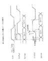
図12は、図11のシステムにおいて、メモリを1個取り出し、それとコントローラ12及びクロック発生回路10の関係を示すようにした図であり、コントローラ12とメモリ13の内部の構成が示されている。図示のように、第1実施例のシステムは、コントローラ12は、クロック発生回路の出力するクロックを受信するクロック入力回路28と、受信したクロックCLKをクロック信号線18に印加するクロック出力回路27と、書込データDinをクロックCLKに同期して出力するデータ出力回路22と、メモリ13から送信されたストローブ信号を受信するストローブ信号入力回路25と、ストローブ信号入力回路25の受信したストローブ信号に同期してメモリ13から送信された読出データDoutを取り込むデータ入力回路23とを有する。また、メモリ13は、コントローラ12から送信されたクロック信号CLKを受信するクロック入力回路37と、書込データDinをクロック信号CLKに同期して取り込むデータ入力回路32と、読出データDoutをクロック入力回路37の出力するクロックCLKに同期して出力するデータ出力回路33と、クロック入力回路37の出力するクロックCLKをストローブ信号として出力するストローブ信号出力回路36とを有する。クロックCLKを伝送するクロック信号線18と、書込データを伝送する書込データバス16aと、読出データを伝送する読出データバス16bと、ストローブ信号を伝送するストローブ信号線17bは、同じ伝搬時間になるように並行に等長配線されている。クロック信号線18とストローブ信号線17bには、伝送するクロック信号とデータストローブ信号をクロックの1/4周期分遅延させるために延長部71と72が設けられている。この延長部71と72は、単にクロック信号線18とストローブ信号線17を長くし、そこを信号が伝搬する時間を長くするものである。このような遅延回路は、DLL回路などの比べて温度などの影響による変動が小さく、遅延量の誤差は小さい。更に、クロック信号線18とストローブ信号線17はインピーダンスが整合されている。
【0034】
図13は図12の第1実施例のシステムにおける書込データの伝送動作を示すタイムチャートである。コントローラ12はクロック出力回路27からクロックCLKを常時出力し、出力書込データの伝送する時には、データ出力回路22からクロックCLKに同期して書込データDin(a)を出力する。ここではDDR方式を使用するから、クロックCLKの立ち上がりエッジと立ち下がりエッジの両方に同期して書込データDin(a)を変化させる。従って、図13に示すように、コントローラ12から出力されたクロックCLK(a)と書込データDin(a)は同じ位相である。
【0035】
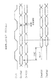
コントローラ12から出力されたクロックCLK(a)と書込データDin(a)は、クロック信号線18と書込データバス16aを通ってメモリ13に伝送される。クロック信号線18には延長部71が設けられているため、ここを通過するとクロックCLK(a)はクロックの1/4周期分遅延され、図示のCLK(a’)になる。従って、クロックCLK(a’)は書込データDin(a)に対してクロックの1/4周期分遅延された信号になり、これらがメモリ13まで伝送される。前述のように、クロック信号線18と書込データバス16aは並行に設けられており、負荷も等しくなるように設定されているので、それらの伝搬時間の差(スキュー)はほとんど無視できる程度である。従って、メモリ13に到着したクロックCLK(b)と書込データDin(b)は、図示のように1/4周期ずれた信号であり、クロックCLK(b)の変化エッジは、書込データDin(b)を取り込むのに最適なタイミングである。従って、データ入力回路32で、クロック入力回路37で取り込んだクロックCLK(b)に同期して書込データDin(b)を取り込めばよい。
【0036】
図14は図12の第1実施例のシステムにおける読出データの伝送動作を示すタイムチャートである。読出データを伝送する時、メモリ13はコントローラ12からコマンドやアドレス信号などのアクセスに必要な信号を受け、内部回路34からデータDoutを読み出す。SDRAMではこのようなアクセス信号に応じて、連続してデータが読み出される。メモリ13は、読出データDoutが読み出された後のクロックCLKの最初の立ち上がりエッジから順次クロックCLKに同期してデータ出力回路33から読出データDoutを出力する。それと同時に、ストローブ信号出力回路36からクロックCLKを出力する。従って、図14に示すように、読出データDout(b)とデータストローブ信号DQS(b)は同じ位相の信号である。
【0037】
メモリ13から出力されたデータストローブ信号DQS(b)と読出データDout(b)は、データストローブ信号線17bと読出データバス16bを通ってコントローラ12に伝送される。前述のように、データストローブ信号線17bと読出データバス16bは並行に設けられており、負荷も等しくなるように設定されているので、それらの伝搬時間の差(スキュー)はほとんど無視できる程度である。しかし、データストローブ信号線17bには延長部72が設けられているため、ここを通過するとデータストローブ信号DQS(b)はクロックの1/4周期分遅延され、図示のDQS(b’)になる。従って、データストローブ信号DQS(b’)は読出データDout(b)に対してクロックの1/4周期分遅延された信号になり、これらがコントローラ12まで伝送される。従って、コントローラ12に到着したデータストローブ信号DQS(a)と読出データDout(a)は、図示のように1/4周期ずれた信号であり、データストローブ信号DQS(a)の変化エッジは、読出データDout(a)を取り込むのに最適なタイミングである。従って、データ入力回路23で、ストローブ信号入力回路25で取り込んだデータストローブ信号DQS(a)に同期して読出データDout(a)を取り込めばよい。
【0038】
以上説明したように、第1実施例では、データを送信する場合に、一緒に送信されるクロック又はデータストローブ信号に同期して送信データが変化され、クロック又はデータストローブ信号は一緒に送信されたデータを取り込むのに適するように途中で位相がずらされる。従って、コントローラ又はメモリでクロック又はデータストローブ信号の位相をずらす必要はなく、DLL回路が必要ない。なお、チップ内部の配線や負荷のために、受信したクロック又はデータストローブ信号をデータ入力回路に供給した場合の遅れが無視できない場合には、受信したクロック又はデータストローブ信号とデータ入力回路に供給する信号の位相を完全に一致させるために0°DLL回路を使用してもよい。その場合でも、0°DLL回路は90°DLL回路に比べてジッタは少なく、精度低下などの問題は生じない。
【0039】
第1実施例では、コントローラ12とメモリ群の間に、クロック信号及びデータストローブ信号を遅延させるための延長部を設けた。信号は1nsで約30cm進むので、例えばクロック周波数が250MHzであれば1/4周期は1nsであり、延長部は15cmを往復する経路が必要である。コントローラとメモリ群は密に配置されているため、コントローラとメモリ群の間にこのようなスペースを取るのが難しい場合がある。第2実施例はそのような条件に対処した実施例である。
【0040】
図15は、第2実施例のメモリサブシステムの構成を示す図であり、(1)が全体構成を、(2)が基本構成を示す。第1実施例と比べて明らかなように、第2実施例のシステムは第1実施例と類似の構成であり、異なるのは、クロック信号線18の延長部71がコントローラ12の外側に、データストローブ信号線17bの延長部72がメモリ群の外側に設けられている点である。クロック発生回路10からコントローラ12にクロックを供給する信号線が設けられているが、この信号線を途中で分岐し、コントローラ12の外側に設けた延長部71の一方に接続する。そして延長部71の他方をクロック信号線18に接続する。各メモリからのデータストローブ信号線は一旦群毎にまとめた上で、コントローラ12に接続されるデータストローブ信号線17bに接続する。例えば、図11の(1)に示した複数のメモリ群が設けられている場合には、各メモリ群毎に延長部72を設け、各群毎にデータストローブ線をまとめた上で対応する延長部72を介してコントローラ12に接続されるデータストローブ線17bに接続する。
【0041】
第1及び第2実施例では、メモリ13は受信したクロックCLKをデータストローブ信号として出力していた。従って、メモリ13に到達したクロックCLKをそのままデータストローブ信号として戻すことも可能である。第3実施例は、データストローブ信号としてクロックCLKを戻すようにした実施例である。
図16は、第3実施例のメモリサブシステムの構成を示す図である。図示のように、第2実施例のシステムと類似の構成を有し、異なるのは、クロック信号線18がメモリ13の部分でストローブ信号線17bに接続され、接続部分にコイルで構成される遅延回路73が設けられている点と、メモリ13にはストローブ信号出力回路が設けられていない点である。遅延回路73は、広く使用されているディレイラインであり、コイルとその前後に設けられた2個のインバータを有する。コイルのインダクタンスを適当に設定することにより、通過する信号を所定量遅延させる。
【0042】
図17と図18は、第3実施例のシステムにおける書込データと読出データの伝送動作を示すタイムチャートである。動作内容は、第1実施例のものとほぼ同じであり、詳しい説明は省略する。
以上、クロックのデューティ比が50%で、クロックの立ち上がりエッジと立ち下がりエッジでデータを出力及び取り込めるとして説明したが、クロックのデューティ比が50%からずれている場合には、コントローラ及びメモリにそれぞれ180°DLL回路を設ける必要がある。しかし、この場合でも1/4周期位相がずれた信号を発生させる必要はない。180°DLL回路は、図10の90°DLL回路51においてディレイ回路を2段とすれば実現でき、90°DLL回路に比べてジッタは半分になる。
【0043】
以上、本発明を、図7に示した片方向ストローブ方式に適用した実施例について説明したが、本発明は同期信号が1方向に送信される信号線を使用する構成であればどのような場合にも適用可能である。
【0044】
【発明の効果】
以上説明したように、本発明によれば、クロック信号線及びデータストローブ信号線に、延長部又はディレイラインなどの遅延回路を設けることにより、コントローラやメモリにDLL回路を搭載せずに、また搭載する場合でも最小限の個数や段数で、データの取込みを良好なタイミングで行うことができる。そのため、ジッタが生じなくなり、ジッタが生じる場合でも小さくできる。
【図面の簡単な説明】
【図1】メモリサブシステムの従来の構成例を示す図である。
【図2】メモリサブシステムの同期方式に関する従来の構成例を示す図である。
【図3】図2のシステムにおけるデータの入出力動作を示すタイムチャートである。
【図4】双方向ストローブ方式のシステムの構成を示す図である。
【図5】双方向ストローブ方式のシステムにおける書込データの伝送動作を示すタイムチャートである。
【図6】双方向ストローブ方式のシステムにおける読出データの伝送動作を示すタイムチャートである。
【図7】従来の片方向ストローブ方式のシステムの構成を示す図である。
【図8】従来の片方向ストローブ方式のシステムにおける書込データの伝送動作を示すタイムチャートである。
【図9】従来の片方向ストローブ方式のシステムにおける読出データの伝送動作を示すタイムチャートである。
【図10】DLL回路を使用したシフトクロック生成回路の構成を示す図である。
【図11】本発明の第1実施例のメモリサブシステムの構成を示す図である。
【図12】第1実施例の基本構成を示す図である。
【図13】第1実施例における書込データの伝送動作を示すタイムチャートである。
【図14】第1実施例における読出データの伝送動作を示すタイムチャートである。
【図15】本発明の第2実施例のメモリサブシステムの構成を示す図である。
【図16】本発明の第3実施例のメモリサブシステムの構成を示す図である。
【図17】第3実施例における書込データの伝送動作を示すタイムチャートである。
【図18】第3実施例における読出データの伝送動作を示すタイムチャートである。
【符号の説明】
10…クロック源(クロック発生回路)
11…クロック分配回路
12…コントローラ
13…メモリ(DIMM)
16…データバス
16a…書込データバス
16b…読出データバス
17b…データストローブ信号線
18…クロック信号線
21、26、31…シフトクロック発生回路
22、33…データ出力回路
23、32…データ入力回路
25…ストローブ信号入力回路
27…クロック出力回路
36…ストローブ信号出力回路
37…クロック入力回路[0001]
BACKGROUND OF THE INVENTION
The present invention relates to a memory subsystem configured by using a memory module that operates in synchronization with a clock or a memory module that functions as a large-capacity memory by mounting a plurality of such memories. The present invention relates to a memory subsystem capable of data transfer.
[0002]
[Prior art]
In a large-scale semiconductor device system such as a computer using a semiconductor device, each part of the system is configured to operate in synchronization with a clock, and a signal such as a data signal or an address signal is input / output to the clock signal. Done synchronously. FIG. 1 is a diagram showing a conventional configuration example of a memory subsystem configured using a memory such as an SDRAM that operates in synchronization with a clock. As shown in the figure, a
[0003]
The
FIG. 2 is a diagram showing the configuration when the number of memories is one in the system of FIG. 1 and the internal configuration of the
[0004]
In the configuration example of (1) in FIG. 2, when data is written to the
[0005]
FIG. 3 is a time chart showing the data input / output operation in the configuration example shown in (1) of FIG. Din and Dout marked with (a) indicate data on the
[0006]
On the other hand, when reading data from the
[0007]
In the configuration shown in FIG. 2A, the
[0008]
In the system of (1) in FIG. 2, the transmission side that outputs the data signal shifts the output timing of the data signal so that the reception side can capture the data signal in synchronization with the clock edge. Is possible. For example, (2) in FIG. 2 is a configuration example in which transmission is performed in synchronization with the clock edge and reception is performed at a timing shifted from the clock edge. When writing data in the configuration of (2) in FIG. 2, the
[0009]
As described above, when the clock frequency is small, the deterioration of the accuracy of the shift
[0010]
Several system configurations for high-speed operation that solve such problems have been proposed, and FIG. 4 is a diagram showing a configuration example of such a system. The system of FIG. 4 uses a method of transmitting data using a data strobe signal DQS separately from the basic clock CLK. The data strobe signal DQS is transmitted by both transmission of write data Din and read data Dout. A method called bi-directional method (bi-directional method) is used. The
[0011]
FIG. 5 is a time chart showing the write data transmission operation in the system of FIG. When transmitting the write data, the
[0012]
FIG. 6 is a time chart showing the read data transmission operation in the system of FIG. When transmitting read data, the
[0013]
As described above, with the bidirectional strobe method shown in FIG. 4, a strobe signal suitable for data acquisition is output in the same direction as the data when data is transmitted in any direction, so transmission is always performed at the optimum timing. Data can be imported. However, like the circuit of FIG. 2, the circuit of FIG. 4 needs to be provided with a shift clock generation circuit for generating two shift clocks shifted by ¼ phase in the
[0014]
FIG. 7 is a diagram illustrating another configuration example of a system for high-speed operation. In this system, a clock CLK is supplied from the
[0015]
FIG. 8 is a time chart showing the write data transmission operation in the system of FIG. The
[0016]
FIG. 9 is a time chart showing the read data transmission operation in the system of FIG. When transmitting read data, the
[0017]
As described above, in the one-way strobe method shown in FIG. 7, transmission data can always be fetched at an optimal timing when data is transmitted in any direction.
As described above, three conventional examples have been described. In any of the conventional examples, it is necessary to generate a shift clock whose phase is shifted by 1/2 of the minimum change period of the data signal. Specifically, if the minimum change period of the data signal is the same as the clock period, a signal whose phase is exactly the same as that of the clock and a signal shifted by ½ period (180 °) are required. In the case of a DDR-SDRAM in which the minimum change period of the data signal is 1/2 of the clock and the data signal changes at both the rising edge and falling edge of the clock, specifically, the phase is 0 or 1 period ( 360 °), 1/4 cycle (90 °), 1/2 cycle (180 °), and 3/4 cycle (270 °) shift clocks must be generated. A DLL (Delay Locked Loop) circuit is used in order to generate such a phase-shifted signal accurately.
[0018]
FIG. 10 is a diagram showing a basic configuration of a DLL circuit that generates a shift clock having an equal phase (0 °) from the clock CLK and a shift clock shifted by ¼ period (90 °). In FIG. 10,
[0019]
The 0 °
[0020]
The 90 °
[0021]
As described above, by using the DLL circuit, it is possible to accurately obtain a signal having a predetermined phase shift. However, the DLL circuit is a complicated circuit having a large circuit scale, a large chip area, and a large power consumption.
[0022]
[Problems to be solved by the invention]
In each of the conventional examples described above, a shift clock generation circuit that generates a signal having a phase difference of, for example, ¼ period is provided in the controller, the memory, or both so that transmission data can be captured at an appropriate timing. In order to accurately generate a signal having a predetermined phase shift, it is necessary to use a DLL circuit. In the case of a DDR-SDRAM, it is necessary to transmit and capture data with reference to both the rising edge and the falling edge.
[0023]
When the duty ratio of the supplied clock is exactly 50%, the rising edge and falling edge of the clock can be used as they are, and a signal whose phase is shifted by 1/4 cycle from the rising edge and falling edge of the clock is generated. . Therefore, the 90 °
When the duty ratio of the clock is deviated from 50%, a signal having a phase difference of 1/2 cycle (180 °) is first generated, and then a signal having a phase shift of 1/4 cycle is generated from the signal. In this case, two DLL circuits are necessary. When such a DLL circuit is used twice, there is a problem that the jitter of the DLL determined by the minimum change amount of the delay circuit is doubled and the accuracy of the shift clock is deteriorated.
[0024]
Therefore, the 90 °
[0025]
Furthermore, the DLL circuit is a complicated circuit as described above. If such a circuit is provided in the controller and the memory, there is a problem that the chip area increases and the cost increases and the power consumption also increases. .
An object of the present invention is to solve such a problem and to realize a memory system capable of high-speed data transmission with a simple configuration.
[0026]
[Means for Solving the Problems]
In order to achieve the above object, the memory subsystem of the present invention outputs data in synchronization with a clock or data strobe signal when data is output from the controller or memory, and is provided in parallel with the data signal line. In a system in which a clock or data strobe signal line transmits a clock or data strobe signal line, a delay circuit that generates a predetermined delay is provided in the clock signal line or data strobe signal line, and a clock or data strobe signal is transmitted to the transmission destination. The signal has a phase suitable for capturing with respect to the data signal, and the data signal can be directly captured by the received clock or data strobe signal. With such a configuration, the above problem does not occur without using a DLL circuit. In addition, as in DDR-SDRAM, even when it is necessary to transmit and capture data based on both the rising edge and falling edge of the clock, only a 180 ° DLL circuit that generates signals having a 180 ° phase difference is used. Since it suffices to provide it, the occurrence of jitter is reduced.
[0027]
That is, the memory subsystem of the present invention includes a controller having an output circuit for outputting a read command and a read data input circuit for fetching read data, a command input circuit for fetching the read command, and a read command corresponding to the read command. A plurality of memories having a read data output circuit for outputting the read data, a clock signal line or a data strobe signal line connected between the controller and the plurality of memories, and the read data to send the read data A data signal line connected between the controller and the plurality of memories, and the controller counts the number of cycles of the clock during an initialization operation, and the controller outputs the read command from the time when the controller outputs the read command. Until the controller fetches the read data from the memory Storing as an access time, allowing the controller to capture the read data at regular timing, wherein the memory subsystem is configured to connect the controller and one of the plurality of memories or between the memories, And further comprising at least one delay circuit disposed on the clock signal line or the data strobe signal line, wherein the delay amount of the at least one delay circuit is such that the access time is approximately equal to an integral multiple of the clock cycle. It is determined to shift.
[0028]
The predetermined delay is a delay in which the clock or data strobe signal becomes a phase suitable for taking in the data signal, and is a half time of the minimum change period of the write data and the read data, and the DDR-SDRAM If this is the case, the delay is 1/4 of the clock period.
The delay circuit can be realized by a circuit having a long wiring so as to lengthen the signal propagation time of the signal line or a delay line using a delay element.
[0029]
The impedance of the clock signal line and the data strobe signal line is preferably matched.
The delay circuit is preferably provided in a portion between the controller and the memory. However, when the delay circuit cannot be provided between the controller and the memory due to space, it can be provided outside the controller and the memory.
[0030]
The clock is applied to the clock signal line from the controller or the clock source. When performing from a clock source, the clock supplied to the controller is branched or performed in parallel.
A clock received by the memory may be used as the data strobe signal. In that case, when the read data is transmitted, the memory changes the read data at the changing edge of the received clock, and the data strobe signal line is connected to the clock signal line near the memory.
[0031]
Conventionally, a shift clock generation circuit is provided in the controller and the memory so that the clock or data strobe signal has a phase suitable for capturing the transmission data. Therefore, the phase cannot be adjusted by lengthening the signal line, and a DLL circuit has to be used. On the other hand, in the present invention, since the phase is adjusted outside the chip, the phase can be adjusted with a simple configuration such as lengthening the signal line.
[0032]
DETAILED DESCRIPTION OF THE INVENTION
FIG. 11 (1) is a diagram showing the overall configuration of the memory subsystem according to the embodiment of the present invention. As shown in (1) of FIG. 11, in the memory subsystem of this embodiment, a clock is supplied from the
A plurality of memories (DIMMs) are connected to one
[0033]
Further, the
FIG. 12 is a diagram in which one memory is taken out from the system of FIG. 11 and shows the relationship between the
[0034]
FIG. 13 is a time chart showing the write data transmission operation in the system of the first embodiment of FIG. The
[0035]
The clock CLK (a) and the write data Din (a) output from the
[0036]
FIG. 14 is a time chart showing the read data transmission operation in the system of the first embodiment of FIG. When transmitting read data, the
[0037]
Data strobe signal DQS (b) and read data Dout (b) output from
[0038]
As described above, in the first embodiment, when data is transmitted, the transmission data is changed in synchronization with the clock or data strobe signal transmitted together, and the clock or data strobe signal is transmitted together. The phase is shifted in the middle to make it suitable for capturing data. Therefore, the controller or memory does not need to shift the phase of the clock or data strobe signal, and no DLL circuit is required. If the delay when the received clock or data strobe signal is supplied to the data input circuit is not negligible due to wiring or a load inside the chip, the received clock or data strobe signal is supplied to the data input circuit. A 0 ° DLL circuit may be used to perfectly match the phase of the signal. Even in such a case, the 0 ° DLL circuit has less jitter than the 90 ° DLL circuit, and does not cause problems such as a decrease in accuracy.
[0039]
In the first embodiment, an extension for delaying the clock signal and the data strobe signal is provided between the
[0040]
FIG. 15 is a diagram showing the configuration of the memory subsystem according to the second embodiment, where (1) shows the overall configuration and (2) shows the basic configuration. As apparent from the comparison with the first embodiment, the system of the second embodiment has a configuration similar to that of the first embodiment except that the
[0041]
In the first and second embodiments, the
FIG. 16 is a diagram showing the configuration of the memory subsystem of the third embodiment. As shown in the figure, it has a configuration similar to that of the system of the second embodiment. The difference is that the
[0042]
17 and 18 are time charts showing the transmission operation of write data and read data in the system of the third embodiment. The content of the operation is almost the same as that of the first embodiment, and detailed description thereof is omitted.
As described above, it has been described that the clock duty ratio is 50%, and data is output and captured at the rising edge and falling edge of the clock. However, if the clock duty ratio deviates from 50%, the controller and the memory It is necessary to provide a 180 ° DLL circuit. However, even in this case, it is not necessary to generate a signal whose phase is shifted by a quarter period. The 180 ° DLL circuit can be realized by using two stages of delay circuits in the 90 °
[0043]
As described above, the embodiment in which the present invention is applied to the one-way strobe method shown in FIG. 7 has been described. However, the present invention is applicable to any configuration as long as it uses a signal line that transmits a synchronization signal in one direction. It is also applicable to.
[0044]
【The invention's effect】
As described above, according to the present invention, a delay circuit such as an extension or a delay line is provided on the clock signal line and the data strobe signal line so that the DLL circuit is not mounted on the controller or the memory. Even in this case, it is possible to fetch data at a good timing with a minimum number of stages and stages. Therefore, jitter does not occur, and even when jitter occurs, it can be reduced.
[Brief description of the drawings]
FIG. 1 is a diagram illustrating a conventional configuration example of a memory subsystem.
FIG. 2 is a diagram illustrating a conventional configuration example regarding a synchronization method of a memory subsystem;
FIG. 3 is a time chart showing data input / output operations in the system of FIG. 2;
FIG. 4 is a diagram showing a configuration of a bidirectional strobe system.
FIG. 5 is a time chart showing a write data transmission operation in a bidirectional strobe system.
FIG. 6 is a time chart showing a read data transmission operation in a bidirectional strobe system.
FIG. 7 is a diagram showing a configuration of a conventional one-way strobe system.
FIG. 8 is a time chart showing a write data transmission operation in a conventional one-way strobe system.
FIG. 9 is a time chart showing a read data transmission operation in a conventional one-way strobe system.
FIG. 10 is a diagram illustrating a configuration of a shift clock generation circuit using a DLL circuit.
FIG. 11 is a diagram showing a configuration of a memory subsystem according to the first exemplary embodiment of the present invention.
FIG. 12 is a diagram showing a basic configuration of the first embodiment.
FIG. 13 is a time chart showing a write data transmission operation in the first embodiment;
FIG. 14 is a time chart showing a read data transmission operation in the first embodiment;
FIG. 15 is a diagram showing a configuration of a memory subsystem according to a second exemplary embodiment of the present invention.
FIG. 16 is a diagram showing a configuration of a memory subsystem according to a third exemplary embodiment of the present invention.
FIG. 17 is a time chart showing a write data transmission operation in the third embodiment;
FIG. 18 is a time chart showing an operation of transmitting read data in the third embodiment.
[Explanation of symbols]
10: Clock source (clock generation circuit)
11 ... Clock distribution circuit
12 ... Controller
13 ... Memory (DIMM)
16: Data bus
16a: Write data bus
16b: Read data bus
17b: Data strobe signal line
18 ... Clock signal line
21, 26, 31... Shift clock generation circuit
22, 33 ... Data output circuit
23, 32 ... Data input circuit
25. Strobe signal input circuit
27. Clock output circuit
36. Strobe signal output circuit
37 ... Clock input circuit
Claims (16)
それぞれが前記読出コマンドを取り込むコマンド入力回路と、前記読出コマンドに応じて前記読出データを出力する読出データ出力回路とを有する複数のメモリと、
前記コントローラと前記複数のメモリの間に接続されたクロック信号線又はデータストローブ信号線と、
前記読出データを送るために前記コントローラと前記複数のメモリの間に接続されたデータ信号線とを備え、
前記コントローラは、初期化動作時に、前記クロックのサイクル数を計数して、前記コントローラが前記読出コマンドを出力する時点から前記コントローラが前記メモリから前記読出データを取り込む時点までのアクセス時間として記憶し、前記コントローラが前記読出データを正規のタイミングで取り込むことを可能にし、
前記コントローラと前記複数のメモリのうちの1つとの間又は前記メモリ間の、前記クロック信号線又は前記データストローブ信号線に配置された少なくとも1つの遅延回路をさらに備え、前記少なくとも1つの遅延回路は、前記アクセス時間が前記クロックの前記サイクルの整数倍にほぼ等しい値から偏移するような遅延時間を有するメモリサブシステム。A controller having an output circuit for outputting a read command and a read data input circuit for fetching read data;
A plurality of memories each having a command input circuit for capturing the read command and a read data output circuit for outputting the read data in response to the read command;
A clock signal line or a data strobe signal line connected between the controller and the plurality of memories;
A data signal line connected between the controller and the plurality of memories for sending the read data;
The controller counts the number of cycles of the clock during an initialization operation, and stores it as an access time from the time when the controller outputs the read command to the time when the controller fetches the read data from the memory, Enabling the controller to capture the read data at regular timing;
And at least one delay circuit disposed on the clock signal line or the data strobe signal line between the controller and one of the plurality of memories or between the memories, the at least one delay circuit comprising: A memory subsystem having a delay time such that the access time deviates from a value approximately equal to an integral multiple of the cycle of the clock.
前記コントローラは、クロックの変化エッジで変化させるように書込データを出力する書込データ出力回路を有し、
各メモリは、調整されたクロックに応じて前記書込データを取り込む書込データ入力回路を有し、
前記読出データ出力回路は、データストローブ信号の変化エッジで変化するように前記読出データを出力し、
前記読出データ入力回路は、調整されたデータストローブ信号に応じて前記読出データを取り込み、
当該メモリサブシステムは、
前記コントローラ及び前記複数のメモリに内蔵されておらず、各メモリの前記書込データ入力回路が前記調整されたクロックの変化エッジで前記書込データを取り込むように、前記クロックを受けて前記調整されたクロックを出力するクロック遅延回路と、
前記コントローラ及び前記複数のメモリに内蔵されておらず、前記コントローラの前記読出データ入力回路が前記調整されたデータストローブ信号の変化エッジで前記読出データを取り込むように、前記データストローブ信号を受けて調整された前記調整されたデータストローブ信号を出力するデータストローブ遅延回路とをさらに備えるメモリサブシステム。The memory subsystem of claim 1, comprising:
The controller has a write data output circuit that outputs write data so as to change at a changing edge of a clock;
Each memory has a write data input circuit that captures the write data in accordance with the adjusted clock,
The read data output circuit outputs the read data so as to change at a change edge of the data strobe signal,
The read data input circuit captures the read data in accordance with the adjusted data strobe signal,
The memory subsystem is
The controller and the plurality of memories are not built in, and the write data input circuit of each memory receives the clock and adjusts the write data so as to capture the write data at the adjusted clock change edge. A clock delay circuit for outputting a clock,
It is not built in the controller and the plurality of memories , and receives and adjusts the data strobe signal so that the read data input circuit of the controller takes in the read data at the changing edge of the adjusted data strobe signal And a data strobe delay circuit for outputting the adjusted data strobe signal.
前記クロック遅延回路の遅延量及び前記データストローブ遅延回路の遅延量は、前記書込データ及び前記読出データの最小変化周期の1/2の時間であるメモリサブシステム。The memory subsystem of claim 2, comprising:
The memory subsystem, wherein a delay amount of the clock delay circuit and a delay amount of the data strobe delay circuit are a half time of a minimum change period of the write data and the read data.
前記クロック遅延回路と前記データストローブ遅延回路は、前記クロック信号線と前記データストローブ信号線の信号伝搬時間を長くするように配線を長くした回路であるメモリサブシステム。A memory subsystem according to claim 2 or 3,
The memory delay system, wherein the clock delay circuit and the data strobe delay circuit are circuits in which wirings are lengthened so as to lengthen the signal propagation time of the clock signal line and the data strobe signal line.
前記クロック遅延回路と前記データストローブ遅延回路は、ディレイ素子を使用したディレイラインであるメモリサブシステム。A memory subsystem according to claim 2 or 3,
The memory subsystem, wherein the clock delay circuit and the data strobe delay circuit are delay lines using delay elements.
前記クロック信号線と前記データストローブ信号線は、インピーダンスが整合しているメモリサブシステム。A memory subsystem according to any one of claims 2 to 5, comprising:
A memory subsystem in which the clock signal line and the data strobe signal line have impedance matching.
前記クロック遅延回路と前記データストローブ遅延回路は、前記クロック信号線と前記データストローブ信号線の前記コントローラと前記メモリの間の部分に設けられているメモリサブシステム。A memory subsystem according to any one of claims 2 to 6, comprising:
The clock delay circuit and the data strobe delay circuit are memory subsystems provided in a portion between the clock signal line and the data strobe signal line between the controller and the memory.
前記クロック遅延回路と前記データストローブ遅延回路は、前記コントローラと前記メモリの間の部分でない外側に設けられているメモリサブシステム。A memory subsystem according to any one of claims 2 to 6, comprising:
The memory delay system, wherein the clock delay circuit and the data strobe delay circuit are provided outside the portion not between the controller and the memory.
前記クロック信号線は前記コントローラから前記メモリに延び、
前記コントローラは、クロック源から供給された前記クロックを、前記クロック信号線に出力するメモリサブシステム。A memory subsystem according to any one of claims 2 to 8, comprising:
The clock signal line extends from the controller to the memory;
The controller is a memory subsystem for outputting the clock supplied from a clock source to the clock signal line.
クロック源から前記コントローラに前記クロックを供給する信号線は、分岐されて前記クロック信号線に接続されているメモリサブシステム。A memory subsystem according to any one of claims 2 to 8, comprising:
A memory subsystem in which a signal line for supplying the clock from a clock source to the controller is branched and connected to the clock signal line.
クロック源から前記クロック信号線に前記クロックを供給する信号線を、前記クロック源から前記コントローラに前記クロックを供給する信号線に並行に設けたメモリサブシステム。A memory subsystem according to any one of claims 2 to 8, comprising:
A memory subsystem in which a signal line for supplying the clock from a clock source to the clock signal line is provided in parallel with a signal line for supplying the clock from the clock source to the controller.
前記データストローブ信号は、前記メモリが受信した前記クロックであり、
前記メモリは、前記コントローラへ読出データを伝送する時には、受信した前記クロックの変化エッジで前記読出データを変化させ、
前記データストローブ信号線は、前記メモリの付近で、前記クロック信号線に接続されているメモリサブシステム。12. A memory subsystem according to any one of claims 2 to 11, comprising:
The data strobe signal is the clock received by the memory;
When the memory transmits read data to the controller, the memory changes the read data at the received change edge of the clock,
The memory subsystem in which the data strobe signal line is connected to the clock signal line in the vicinity of the memory.
前記クロックを供給するクロック源と、
前記コントローラと前記複数のメモリの間で前記書き込み及び読出データ信号を伝送するデータ信号線と、
前記データ信号線に並行に設けられ、前記複数のメモリへ前記調整されたクロックを伝送するクロック信号線と、
前記データ信号線に並行に設けられ、前記コントローラへ前記調整されたデータストローブ信号を伝送するデータストローブ信号線とを備え、
前記クロック信号線は前記クロック遅延回路を有し、前記データストローブ信号線は前記データストローブ遅延回路を有し、前記クロックは前記クロック信号線を介して前記クロック遅延回路に供給され、前記データストローブ信号は前記データストローブ信号線を介して前記データストローブ遅延回路に供給されるメモリサブシステム。The memory subsystem of claim 2, comprising:
A clock source for supplying the clock;
A data signal line for transmitting the write and read data signals between the controller and the plurality of memories;
A clock signal line that is provided in parallel to the data signal line and transmits the adjusted clock to the plurality of memories;
A data strobe signal line provided in parallel to the data signal line and transmitting the adjusted data strobe signal to the controller;
The clock signal line includes the clock delay circuit, the data strobe signal line includes the data strobe delay circuit, the clock is supplied to the clock delay circuit via the clock signal line, and the data strobe signal Is a memory subsystem supplied to the data strobe delay circuit via the data strobe signal line.
前記コントローラの前記読出データ入力回路は、調整されたデータストローブ信号に応じて前記読出データを取り込み、
各メモリは、前記データストローブ信号の変化エッジで変化させるように前記読出データを出力し、
当該サブシステムは、
前記コントローラ及び前記複数のメモリに内蔵されておらず、前記コントローラの前記読出データ入力回路が前記調整されたデータストローブ信号の変化エッジで前記読出データを取り込むように、前記データストローブ信号を受けて調整された前記調整されたデータストローブ信号を出力するデータストローブ遅延回路をさらに備えるメモリサブシステム。The memory subsystem of claim 1, comprising:
The read data input circuit of the controller takes in the read data in accordance with the adjusted data strobe signal,
Each memory outputs the read data so as to change at the changing edge of the data strobe signal,
The subsystem is
It is not built in the controller and the plurality of memories, and receives and adjusts the data strobe signal so that the read data input circuit of the controller takes in the read data at the changing edge of the adjusted data strobe signal A memory subsystem further comprising a data strobe delay circuit for outputting the adjusted data strobe signal.
それぞれが前記読出コマンドを取り込み、前記読出コマンドに応じて前記読出データを出力する複数のメモリデバイスと、
前記コントローラと前記複数のメモリデバイスの間に接続されたクロック信号線又はデータストローブ信号線と、
前記読出データを送るために前記コントローラと前記複数のメモリデバイスの間に接続されたデータ信号線とを備え、
前記コントローラは、初期化動作時に、クロックのサイクル数を計数して、前記コントローラが前記読出コマンドを出力する時点から前記コントローラが各メモリデバイスから前記読出データを取り込む時点までのアクセス時間として記憶し、前記コントローラが前記読出データを正規のタイミングで取り込むことを可能にし、
前記コントローラと前記複数のメモリデバイスのうちの選択された1つとの間の、前記クロック信号線又は前記データストローブ信号線に配置された遅延回路をさらに備え、前記遅延回路の遅延量は、前記アクセス時間が前記クロックの前記サイクルの整数倍にほぼ等しい値から偏移するような遅延時間を有するメモリサブシステム。A controller that outputs a read command to capture read data;
A plurality of memory devices each taking in the read command and outputting the read data in response to the read command;
A clock signal line or a data strobe signal line connected between the controller and the plurality of memory devices;
A data signal line connected between the controller and the plurality of memory devices for sending the read data;
The controller counts the number of clock cycles during an initialization operation and stores it as an access time from the time when the controller outputs the read command to the time when the controller fetches the read data from each memory device. Enabling the controller to capture the read data at regular timing;
Between a selected one of said the previous SL controller plurality of memory devices, further comprising a delay circuit arranged in the clock signal line or the data strobe signal line, the delay amount of the delay circuit, the A memory subsystem having a delay time such that the access time deviates from a value approximately equal to an integral multiple of the cycle of the clock.
前記コントローラは、クロックの変化エッジで変化させるように書き込みデータを出力する書き込みデータ出力回路を有し、
当該メモリサブシステムは、
調整されたクロックに応じて前記書き込みデータを取り込む書き込みデータ入力回路を有するメモリデバイスと、
前記コントローラ及び前記複数のメモリデバイスに内蔵されておらず、各メモリデバイスの前記書き込みデータ入力回路が前記調整されたクロックの変化エッジで前記書き込みデータを取り込むように、前記クロックを受けて前記調整されたクロックを出力するクロック遅延回路とをさらに備えるメモリサブシステム。The memory subsystem of claim 15, comprising:
The controller has a write data output circuit that outputs write data so as to change at a changing edge of a clock;
The memory subsystem is
A memory device having a write data input circuit that captures the write data in accordance with the adjusted clock;
It is not built in the controller and the plurality of memory devices, and is adjusted by receiving the clock so that the write data input circuit of each memory device captures the write data at the changing edge of the adjusted clock. And a clock delay circuit for outputting a clock.
Priority Applications (4)
| Application Number | Priority Date | Filing Date | Title |
|---|---|---|---|
| JP17996997A JP3929116B2 (en) | 1997-07-04 | 1997-07-04 | Memory subsystem |
| US08/970,086 US6397312B1 (en) | 1997-07-04 | 1997-11-13 | Memory subsystem operated in synchronism with a clock |
| TW086116931A TW351787B (en) | 1997-07-04 | 1997-11-13 | Memory subsystem capable of high speed data transfer |
| KR1019970063317A KR100271724B1 (en) | 1997-07-04 | 1997-11-27 | Memory subsystem |
Applications Claiming Priority (1)
| Application Number | Priority Date | Filing Date | Title |
|---|---|---|---|
| JP17996997A JP3929116B2 (en) | 1997-07-04 | 1997-07-04 | Memory subsystem |
Publications (2)
| Publication Number | Publication Date |
|---|---|
| JPH1125029A JPH1125029A (en) | 1999-01-29 |
| JP3929116B2 true JP3929116B2 (en) | 2007-06-13 |
Family
ID=16075154
Family Applications (1)
| Application Number | Title | Priority Date | Filing Date |
|---|---|---|---|
| JP17996997A Expired - Fee Related JP3929116B2 (en) | 1997-07-04 | 1997-07-04 | Memory subsystem |
Country Status (4)
| Country | Link |
|---|---|
| US (1) | US6397312B1 (en) |
| JP (1) | JP3929116B2 (en) |
| KR (1) | KR100271724B1 (en) |
| TW (1) | TW351787B (en) |
Families Citing this family (44)
| Publication number | Priority date | Publication date | Assignee | Title |
|---|---|---|---|---|
| US6314527B1 (en) * | 1998-03-05 | 2001-11-06 | Micron Technology, Inc. | Recovery of useful areas of partially defective synchronous memory components |
| US6621496B1 (en) * | 1999-02-26 | 2003-09-16 | Micron Technology, Inc. | Dual mode DDR SDRAM/SGRAM |
| KR100447051B1 (en) * | 1999-05-31 | 2004-09-04 | 미쓰비시덴키 가부시키가이샤 | Data transfer system |
| DE19926075A1 (en) * | 1999-06-08 | 2000-12-14 | Endress Hauser Gmbh Co | Procedure for the temporal coordination of the sending of data on a bus |
| JP4353324B2 (en) * | 1999-08-31 | 2009-10-28 | エルピーダメモリ株式会社 | Semiconductor device |
| JP4707204B2 (en) * | 1999-10-08 | 2011-06-22 | 富士通セミコンダクター株式会社 | Semiconductor memory device |
| US6621760B1 (en) * | 2000-01-13 | 2003-09-16 | Intel Corporation | Method, apparatus, and system for high speed data transfer using source synchronous data strobe |
| JP4778132B2 (en) * | 2000-05-19 | 2011-09-21 | 富士通セミコンダクター株式会社 | Memory controller and system |
| US6611905B1 (en) * | 2000-06-29 | 2003-08-26 | International Business Machines Corporation | Memory interface with programable clock to output time based on wide range of receiver loads |
| US7017070B1 (en) * | 2000-10-13 | 2006-03-21 | Ati International Srl | Apparatus for synchronization of double data rate signaling |
| US6553472B2 (en) * | 2001-01-12 | 2003-04-22 | Sun Microsystems, Inc. | Method for programming clock delays, command delays, read command parameter delays, and write command parameter delays of a memory controller in a high performance microprocessor |
| US7313715B2 (en) * | 2001-02-09 | 2007-12-25 | Samsung Electronics Co., Ltd. | Memory system having stub bus configuration |
| KR100382736B1 (en) * | 2001-03-09 | 2003-05-09 | 삼성전자주식회사 | Semiconductor memory device having different data rates in read operation and write operation |
| US20030120989A1 (en) * | 2001-12-26 | 2003-06-26 | Zumkehr John F. | Method and circuit to implement double data rate testing |
| US6597202B1 (en) * | 2001-12-28 | 2003-07-22 | Intel Corporation | Systems with skew control between clock and data signals |
| US6819599B2 (en) * | 2002-08-01 | 2004-11-16 | Micron Technology, Inc. | Programmable DQS preamble |
| DE10344959A1 (en) * | 2003-09-27 | 2005-04-28 | Infineon Technologies Ag | RAM memory circuit for scanning received data has selectively addressable memory cells, a data connection, an address input to select memory cells, a command input and a clock input |
| US20050071707A1 (en) * | 2003-09-30 | 2005-03-31 | Hampel Craig E. | Integrated circuit with bi-modal data strobe |
| DE10354034B4 (en) * | 2003-11-19 | 2005-12-08 | Infineon Technologies Ag | A method of operating a semiconductor memory device and semiconductor memory device |
| US7126874B2 (en) * | 2004-08-31 | 2006-10-24 | Micron Technology, Inc. | Memory system and method for strobing data, command and address signals |
| KR100640594B1 (en) * | 2004-10-27 | 2006-11-01 | 삼성전자주식회사 | Interface circuit and memory system for implementing adaptive DQS latch scheme |
| KR100562645B1 (en) * | 2004-10-29 | 2006-03-20 | 주식회사 하이닉스반도체 | Semiconductor memory device |
| JP4785465B2 (en) * | 2005-08-24 | 2011-10-05 | ルネサスエレクトロニクス株式会社 | Interface circuit and semiconductor device |
| US7269093B2 (en) * | 2005-10-31 | 2007-09-11 | Infineon Technologies Ag | Generating a sampling clock signal in a communication block of a memory device |
| US7907472B2 (en) | 2006-08-24 | 2011-03-15 | Panasonic Corporation | Semiconductor integrated circuit for fetching read data from a DDR-SDRAM operating in synchronization with a clock |
| US7666160B2 (en) * | 2006-12-29 | 2010-02-23 | Kimberly-Clark Worldwide, Inc. | Delivery device |
| JP4325685B2 (en) * | 2007-02-21 | 2009-09-02 | セイコーエプソン株式会社 | MEMORY CONTROLLER, MEMORY MODULE, MEMORY CONTROL METHOD, AND COMPUTER FOR CONTROLLING MEMORY |
| US7586355B2 (en) * | 2007-07-11 | 2009-09-08 | United Memories, Inc. | Low skew clock distribution tree |
| CN101373639B (en) * | 2007-08-22 | 2011-02-09 | 智原科技股份有限公司 | Memory time sequence measuring circuit and test method thereof |
| EP2518629A4 (en) | 2009-12-25 | 2013-08-07 | Fujitsu Ltd | Signal receiving circuit, memory controller, processor, computer, and phase control method |
| JP5331902B2 (en) | 2009-12-25 | 2013-10-30 | 富士通株式会社 | Signal restoration circuit, latency adjustment circuit, memory controller, processor, computer, signal restoration method, and latency adjustment method |
| JP5320345B2 (en) * | 2010-06-09 | 2013-10-23 | 株式会社村田製作所 | Wiring board |
| US8782459B2 (en) | 2011-06-21 | 2014-07-15 | Via Technologies, Inc. | Apparatus and method for advanced synchronous strobe transmission |
| US8751850B2 (en) | 2011-06-21 | 2014-06-10 | Via Technologies, Inc. | Optimized synchronous data reception mechanism |
| US8839018B2 (en) | 2011-06-21 | 2014-09-16 | Via Technologies, Inc. | Programmable mechanism for optimizing a synchronous data bus |
| US8683253B2 (en) * | 2011-06-21 | 2014-03-25 | Via Technologies, Inc. | Optimized synchronous strobe transmission mechanism |
| US8782460B2 (en) | 2011-06-21 | 2014-07-15 | Via Technologies, Inc. | Apparatus and method for delayed synchronous data reception |
| US8751851B2 (en) | 2011-06-21 | 2014-06-10 | Via Technologies, Inc. | Programmable mechanism for synchronous strobe advance |
| US8751852B2 (en) | 2011-06-21 | 2014-06-10 | Via Technologies, Inc. | Programmable mechanism for delayed synchronous data reception |
| CN102946293B (en) * | 2012-09-26 | 2015-09-23 | 中国航天科技集团公司第九研究院第七七一研究所 | A kind of parallel receive method based on DS coding and device thereof |
| US9111607B2 (en) * | 2013-05-31 | 2015-08-18 | Freescale Semiconductor, Inc. | Multiple data rate memory with read timing information |
| JP6207551B2 (en) * | 2015-07-10 | 2017-10-04 | 株式会社メガチップス | Memory system |
| JP6188246B2 (en) * | 2015-07-10 | 2017-08-30 | 株式会社メガチップス | Memory system |
| CN107977328B (en) * | 2017-12-20 | 2019-12-10 | 天津瑞发科半导体技术有限公司 | ONFI interface double-clock edge sampling device |
Family Cites Families (31)
| Publication number | Priority date | Publication date | Assignee | Title |
|---|---|---|---|---|
| KR960003526B1 (en) * | 1992-10-02 | 1996-03-14 | 삼성전자주식회사 | Semiconductor memory device |
| FR2460526A1 (en) * | 1979-06-29 | 1981-01-23 | Ibm France | METHOD FOR MEASURING THE MEMORY ADDRESS ACCESS TIME USING THE DATA RECIRCULATION TECHNIQUE, AND TESTER RESULTING THEREFROM |
| DE3501569C2 (en) * | 1984-01-20 | 1996-07-18 | Canon Kk | Data processing device |
| US5278974A (en) * | 1989-12-04 | 1994-01-11 | Digital Equipment Corporation | Method and apparatus for the dynamic adjustment of data transfer timing to equalize the bandwidths of two buses in a computer system having different bandwidths |
| US5239639A (en) * | 1990-11-09 | 1993-08-24 | Intel Corporation | Efficient memory controller with an independent clock |
| US5608896A (en) * | 1992-05-28 | 1997-03-04 | Texas Instruments Incorporated | Time skewing arrangement for operating memory devices in synchronism with a data processor |
| US5615355A (en) * | 1992-10-22 | 1997-03-25 | Ampex Corporation | Method and apparatus for buffering a user application from the timing requirements of a DRAM |
| US5479647A (en) * | 1993-11-12 | 1995-12-26 | Intel Corporation | Clock generation and distribution system for a memory controller with a CPU interface for synchronizing the CPU interface with a microprocessor external to the memory controller |
| US5815016A (en) * | 1994-09-02 | 1998-09-29 | Xilinx, Inc. | Phase-locked delay loop for clock correction |
| US5796673A (en) * | 1994-10-06 | 1998-08-18 | Mosaid Technologies Incorporated | Delay locked loop implementation in a synchronous dynamic random access memory |
| US5623638A (en) * | 1994-11-22 | 1997-04-22 | Advanced Micro Devices, Inc. | Memory control unit with programmable edge generator to minimize delay periods for critical DRAM timing parameters |
| US5577236A (en) * | 1994-12-30 | 1996-11-19 | International Business Machines Corporation | Memory controller for reading data from synchronous RAM |
| US5692165A (en) * | 1995-09-12 | 1997-11-25 | Micron Electronics Inc. | Memory controller with low skew control signal |
| JP3455040B2 (en) * | 1996-12-16 | 2003-10-06 | 株式会社日立製作所 | Source clock synchronous memory system and memory unit |
| US5923611A (en) * | 1996-12-20 | 1999-07-13 | Micron Technology, Inc. | Memory having a plurality of external clock signal inputs |
| JP3979690B2 (en) | 1996-12-27 | 2007-09-19 | 富士通株式会社 | Semiconductor memory device system and semiconductor memory device |
| JPH10241362A (en) * | 1997-02-25 | 1998-09-11 | Mitsubishi Electric Corp | Synchronous semiconductor memory and logical semiconductor device |
| US5987576A (en) * | 1997-02-27 | 1999-11-16 | Hewlett-Packard Company | Method and apparatus for generating and distributing clock signals with minimal skew |
| US6044474A (en) * | 1997-04-08 | 2000-03-28 | Klein; Dean A. | Memory controller with buffered CAS/RAS external synchronization capability for reducing the effects of clock-to-signal skew |
| JPH10308093A (en) * | 1997-05-07 | 1998-11-17 | Mitsubishi Electric Corp | Input signal phase compensating circuit |
| US5946712A (en) * | 1997-06-04 | 1999-08-31 | Oak Technology, Inc. | Apparatus and method for reading data from synchronous memory |
| JPH1174783A (en) * | 1997-06-18 | 1999-03-16 | Mitsubishi Electric Corp | Internal clock signal generation circuit and synchronous semiconductor memory device |
| JP3922765B2 (en) * | 1997-07-22 | 2007-05-30 | 富士通株式会社 | Semiconductor device system and semiconductor device |
| JP3211739B2 (en) * | 1997-08-25 | 2001-09-25 | 日本電気株式会社 | Semiconductor storage device |
| US6185664B1 (en) * | 1997-11-17 | 2001-02-06 | Micron Technology, Inc. | Method for providing additional latency for synchronously accessed memory |
| US6003118A (en) * | 1997-12-16 | 1999-12-14 | Acer Laboratories Inc. | Method and apparatus for synchronizing clock distribution of a data processing system |
| US6072743A (en) * | 1998-01-13 | 2000-06-06 | Mitsubishi Denki Kabushiki Kaisha | High speed operable semiconductor memory device with memory blocks arranged about the center |
| US6105144A (en) * | 1998-03-02 | 2000-08-15 | International Business Machines Corporation | System and method for alleviating skew in a bus |
| US5923613A (en) * | 1998-03-18 | 1999-07-13 | Etron Technology, Inc. | Latched type clock synchronizer with additional 180°-phase shift clock |
| US6016282A (en) * | 1998-05-28 | 2000-01-18 | Micron Technology, Inc. | Clock vernier adjustment |
| US6043694A (en) * | 1998-06-24 | 2000-03-28 | Siemens Aktiengesellschaft | Lock arrangement for a calibrated DLL in DDR SDRAM applications |
-
1997
- 1997-07-04 JP JP17996997A patent/JP3929116B2/en not_active Expired - Fee Related
- 1997-11-13 TW TW086116931A patent/TW351787B/en not_active IP Right Cessation
- 1997-11-13 US US08/970,086 patent/US6397312B1/en not_active Expired - Lifetime
- 1997-11-27 KR KR1019970063317A patent/KR100271724B1/en not_active IP Right Cessation
Also Published As
| Publication number | Publication date |
|---|---|
| TW351787B (en) | 1999-02-01 |
| US6397312B1 (en) | 2002-05-28 |
| KR19990013250A (en) | 1999-02-25 |
| KR100271724B1 (en) | 2000-11-15 |
| JPH1125029A (en) | 1999-01-29 |
Similar Documents
| Publication | Publication Date | Title |
|---|---|---|
| JP3929116B2 (en) | Memory subsystem | |
| US6446158B1 (en) | Memory system using FET switches to select memory banks | |
| JP3979690B2 (en) | Semiconductor memory device system and semiconductor memory device | |
| JP4159415B2 (en) | Memory module and memory system | |
| JP4808414B2 (en) | Computer system and memory system | |
| JP4070051B2 (en) | Data masking method and circuit for semiconductor memory device, and semiconductor memory device having the circuit | |
| JP4212281B2 (en) | Memory system with PTP bus configuration | |
| KR100626375B1 (en) | Semiconductor memory device and module for high frequency operation | |
| WO1999046687A1 (en) | Data transmitter | |
| KR20030033070A (en) | System and method for providing reliable transmission in a buffered memory system | |
| JP2005209168A (en) | Semiconductor memory module, memory system, circuit, semiconductor device and dimm | |
| KR100281952B1 (en) | Data transfer memory device | |
| WO2005106888A1 (en) | Multiple data rate ram memory controller | |
| JP4305616B2 (en) | Control and address clock non-distributed memory system | |
| JP4136577B2 (en) | Memory control device and data processing device | |
| JPH09179819A (en) | Synchronous data transfer system | |
| KR100408397B1 (en) | Memory device having exterior delay control mechanism for adjusting internal clock of data processing and memory module including the same | |
| JP4952177B2 (en) | Storage device | |
| KR100546097B1 (en) | Control and Address Clock Non-Distributed Memory System | |
| JP2006065470A (en) | Memory control method and device | |
| JP2008123543A (en) | Data transmission method, system and device | |
| JPH10187592A (en) | Memory bus system | |
| KR20070044129A (en) | Structure of data signal line in semiconductor memory device |
Legal Events
| Date | Code | Title | Description |
|---|---|---|---|
| A977 | Report on retrieval |
Free format text: JAPANESE INTERMEDIATE CODE: A971007 Effective date: 20060328 |
|
| A131 | Notification of reasons for refusal |
Free format text: JAPANESE INTERMEDIATE CODE: A131 Effective date: 20060404 |
|
| A521 | Written amendment |
Free format text: JAPANESE INTERMEDIATE CODE: A523 Effective date: 20060519 |
|
| A131 | Notification of reasons for refusal |
Free format text: JAPANESE INTERMEDIATE CODE: A131 Effective date: 20061121 |
|
| A521 | Written amendment |
Free format text: JAPANESE INTERMEDIATE CODE: A523 Effective date: 20070119 |
|
| TRDD | Decision of grant or rejection written | ||
| A01 | Written decision to grant a patent or to grant a registration (utility model) |
Free format text: JAPANESE INTERMEDIATE CODE: A01 Effective date: 20070206 |
|
| A61 | First payment of annual fees (during grant procedure) |
Free format text: JAPANESE INTERMEDIATE CODE: A61 Effective date: 20070306 |
|
| R150 | Certificate of patent or registration of utility model |
Free format text: JAPANESE INTERMEDIATE CODE: R150 |
|
| S111 | Request for change of ownership or part of ownership |
Free format text: JAPANESE INTERMEDIATE CODE: R313111 |
|
| FPAY | Renewal fee payment (event date is renewal date of database) |
Free format text: PAYMENT UNTIL: 20100316 Year of fee payment: 3 |
|
| R350 | Written notification of registration of transfer |
Free format text: JAPANESE INTERMEDIATE CODE: R350 |
|
| FPAY | Renewal fee payment (event date is renewal date of database) |
Free format text: PAYMENT UNTIL: 20100316 Year of fee payment: 3 |
|
| FPAY | Renewal fee payment (event date is renewal date of database) |
Free format text: PAYMENT UNTIL: 20110316 Year of fee payment: 4 |
|
| FPAY | Renewal fee payment (event date is renewal date of database) |
Free format text: PAYMENT UNTIL: 20110316 Year of fee payment: 4 |
|
| S531 | Written request for registration of change of domicile |
Free format text: JAPANESE INTERMEDIATE CODE: R313531 |
|
| S533 | Written request for registration of change of name |
Free format text: JAPANESE INTERMEDIATE CODE: R313533 |
|
| FPAY | Renewal fee payment (event date is renewal date of database) |
Free format text: PAYMENT UNTIL: 20110316 Year of fee payment: 4 |
|
| R350 | Written notification of registration of transfer |
Free format text: JAPANESE INTERMEDIATE CODE: R350 |
|
| FPAY | Renewal fee payment (event date is renewal date of database) |
Free format text: PAYMENT UNTIL: 20110316 Year of fee payment: 4 |
|
| FPAY | Renewal fee payment (event date is renewal date of database) |
Free format text: PAYMENT UNTIL: 20120316 Year of fee payment: 5 |
|
| FPAY | Renewal fee payment (event date is renewal date of database) |
Free format text: PAYMENT UNTIL: 20130316 Year of fee payment: 6 |
|
| FPAY | Renewal fee payment (event date is renewal date of database) |
Free format text: PAYMENT UNTIL: 20140316 Year of fee payment: 7 |
|
| S111 | Request for change of ownership or part of ownership |
Free format text: JAPANESE INTERMEDIATE CODE: R313111 |
|
| R350 | Written notification of registration of transfer |
Free format text: JAPANESE INTERMEDIATE CODE: R350 |
|
| LAPS | Cancellation because of no payment of annual fees |