JP3856426B2 - Semiconductor device and manufacturing method thereof - Google Patents
Semiconductor device and manufacturing method thereof Download PDFInfo
- Publication number
- JP3856426B2 JP3856426B2 JP2001271255A JP2001271255A JP3856426B2 JP 3856426 B2 JP3856426 B2 JP 3856426B2 JP 2001271255 A JP2001271255 A JP 2001271255A JP 2001271255 A JP2001271255 A JP 2001271255A JP 3856426 B2 JP3856426 B2 JP 3856426B2
- Authority
- JP
- Japan
- Prior art keywords
- electrode pad
- insulating film
- interlayer insulating
- opening
- wire bonding
- Prior art date
- Legal status (The legal status is an assumption and is not a legal conclusion. Google has not performed a legal analysis and makes no representation as to the accuracy of the status listed.)
- Expired - Fee Related
Links
Images


Classifications
-
- H—ELECTRICITY
- H01—ELECTRIC ELEMENTS
- H01L—SEMICONDUCTOR DEVICES NOT COVERED BY CLASS H10
- H01L24/00—Arrangements for connecting or disconnecting semiconductor or solid-state bodies; Methods or apparatus related thereto
- H01L24/01—Means for bonding being attached to, or being formed on, the surface to be connected, e.g. chip-to-package, die-attach, "first-level" interconnects; Manufacturing methods related thereto
- H01L24/02—Bonding areas ; Manufacturing methods related thereto
- H01L24/04—Structure, shape, material or disposition of the bonding areas prior to the connecting process
- H01L24/05—Structure, shape, material or disposition of the bonding areas prior to the connecting process of an individual bonding area
-
- H—ELECTRICITY
- H01—ELECTRIC ELEMENTS
- H01L—SEMICONDUCTOR DEVICES NOT COVERED BY CLASS H10
- H01L22/00—Testing or measuring during manufacture or treatment; Reliability measurements, i.e. testing of parts without further processing to modify the parts as such; Structural arrangements therefor
- H01L22/30—Structural arrangements specially adapted for testing or measuring during manufacture or treatment, or specially adapted for reliability measurements
- H01L22/32—Additional lead-in metallisation on a device or substrate, e.g. additional pads or pad portions, lines in the scribe line, sacrificed conductors
-
- H—ELECTRICITY
- H01—ELECTRIC ELEMENTS
- H01L—SEMICONDUCTOR DEVICES NOT COVERED BY CLASS H10
- H01L24/00—Arrangements for connecting or disconnecting semiconductor or solid-state bodies; Methods or apparatus related thereto
- H01L24/01—Means for bonding being attached to, or being formed on, the surface to be connected, e.g. chip-to-package, die-attach, "first-level" interconnects; Manufacturing methods related thereto
- H01L24/02—Bonding areas ; Manufacturing methods related thereto
- H01L24/03—Manufacturing methods
-
- H—ELECTRICITY
- H01—ELECTRIC ELEMENTS
- H01L—SEMICONDUCTOR DEVICES NOT COVERED BY CLASS H10
- H01L2224/00—Indexing scheme for arrangements for connecting or disconnecting semiconductor or solid-state bodies and methods related thereto as covered by H01L24/00
- H01L2224/01—Means for bonding being attached to, or being formed on, the surface to be connected, e.g. chip-to-package, die-attach, "first-level" interconnects; Manufacturing methods related thereto
- H01L2224/02—Bonding areas; Manufacturing methods related thereto
- H01L2224/0212—Auxiliary members for bonding areas, e.g. spacers
- H01L2224/02122—Auxiliary members for bonding areas, e.g. spacers being formed on the semiconductor or solid-state body
- H01L2224/02163—Auxiliary members for bonding areas, e.g. spacers being formed on the semiconductor or solid-state body on the bonding area
- H01L2224/02165—Reinforcing structures
- H01L2224/02166—Collar structures
-
- H—ELECTRICITY
- H01—ELECTRIC ELEMENTS
- H01L—SEMICONDUCTOR DEVICES NOT COVERED BY CLASS H10
- H01L2224/00—Indexing scheme for arrangements for connecting or disconnecting semiconductor or solid-state bodies and methods related thereto as covered by H01L24/00
- H01L2224/01—Means for bonding being attached to, or being formed on, the surface to be connected, e.g. chip-to-package, die-attach, "first-level" interconnects; Manufacturing methods related thereto
- H01L2224/02—Bonding areas; Manufacturing methods related thereto
- H01L2224/03—Manufacturing methods
- H01L2224/039—Methods of manufacturing bonding areas involving a specific sequence of method steps
- H01L2224/0392—Methods of manufacturing bonding areas involving a specific sequence of method steps specifically adapted to include a probing step
- H01L2224/03921—Methods of manufacturing bonding areas involving a specific sequence of method steps specifically adapted to include a probing step by repairing the bonding area damaged by the probing step
-
- H—ELECTRICITY
- H01—ELECTRIC ELEMENTS
- H01L—SEMICONDUCTOR DEVICES NOT COVERED BY CLASS H10
- H01L2224/00—Indexing scheme for arrangements for connecting or disconnecting semiconductor or solid-state bodies and methods related thereto as covered by H01L24/00
- H01L2224/01—Means for bonding being attached to, or being formed on, the surface to be connected, e.g. chip-to-package, die-attach, "first-level" interconnects; Manufacturing methods related thereto
- H01L2224/02—Bonding areas; Manufacturing methods related thereto
- H01L2224/04—Structure, shape, material or disposition of the bonding areas prior to the connecting process
- H01L2224/04042—Bonding areas specifically adapted for wire connectors, e.g. wirebond pads
-
- H—ELECTRICITY
- H01—ELECTRIC ELEMENTS
- H01L—SEMICONDUCTOR DEVICES NOT COVERED BY CLASS H10
- H01L2224/00—Indexing scheme for arrangements for connecting or disconnecting semiconductor or solid-state bodies and methods related thereto as covered by H01L24/00
- H01L2224/01—Means for bonding being attached to, or being formed on, the surface to be connected, e.g. chip-to-package, die-attach, "first-level" interconnects; Manufacturing methods related thereto
- H01L2224/02—Bonding areas; Manufacturing methods related thereto
- H01L2224/04—Structure, shape, material or disposition of the bonding areas prior to the connecting process
- H01L2224/05—Structure, shape, material or disposition of the bonding areas prior to the connecting process of an individual bonding area
- H01L2224/05001—Internal layers
- H01L2224/05075—Plural internal layers
- H01L2224/0508—Plural internal layers being stacked
- H01L2224/05082—Two-layer arrangements
-
- H—ELECTRICITY
- H01—ELECTRIC ELEMENTS
- H01L—SEMICONDUCTOR DEVICES NOT COVERED BY CLASS H10
- H01L2224/00—Indexing scheme for arrangements for connecting or disconnecting semiconductor or solid-state bodies and methods related thereto as covered by H01L24/00
- H01L2224/01—Means for bonding being attached to, or being formed on, the surface to be connected, e.g. chip-to-package, die-attach, "first-level" interconnects; Manufacturing methods related thereto
- H01L2224/02—Bonding areas; Manufacturing methods related thereto
- H01L2224/04—Structure, shape, material or disposition of the bonding areas prior to the connecting process
- H01L2224/05—Structure, shape, material or disposition of the bonding areas prior to the connecting process of an individual bonding area
- H01L2224/0554—External layer
- H01L2224/0555—Shape
- H01L2224/05552—Shape in top view
- H01L2224/05553—Shape in top view being rectangular
-
- H—ELECTRICITY
- H01—ELECTRIC ELEMENTS
- H01L—SEMICONDUCTOR DEVICES NOT COVERED BY CLASS H10
- H01L2224/00—Indexing scheme for arrangements for connecting or disconnecting semiconductor or solid-state bodies and methods related thereto as covered by H01L24/00
- H01L2224/01—Means for bonding being attached to, or being formed on, the surface to be connected, e.g. chip-to-package, die-attach, "first-level" interconnects; Manufacturing methods related thereto
- H01L2224/02—Bonding areas; Manufacturing methods related thereto
- H01L2224/04—Structure, shape, material or disposition of the bonding areas prior to the connecting process
- H01L2224/05—Structure, shape, material or disposition of the bonding areas prior to the connecting process of an individual bonding area
- H01L2224/0554—External layer
- H01L2224/0555—Shape
- H01L2224/05552—Shape in top view
- H01L2224/05554—Shape in top view being square
-
- H—ELECTRICITY
- H01—ELECTRIC ELEMENTS
- H01L—SEMICONDUCTOR DEVICES NOT COVERED BY CLASS H10
- H01L2224/00—Indexing scheme for arrangements for connecting or disconnecting semiconductor or solid-state bodies and methods related thereto as covered by H01L24/00
- H01L2224/01—Means for bonding being attached to, or being formed on, the surface to be connected, e.g. chip-to-package, die-attach, "first-level" interconnects; Manufacturing methods related thereto
- H01L2224/02—Bonding areas; Manufacturing methods related thereto
- H01L2224/04—Structure, shape, material or disposition of the bonding areas prior to the connecting process
- H01L2224/05—Structure, shape, material or disposition of the bonding areas prior to the connecting process of an individual bonding area
- H01L2224/0554—External layer
- H01L2224/05599—Material
- H01L2224/056—Material with a principal constituent of the material being a metal or a metalloid, e.g. boron [B], silicon [Si], germanium [Ge], arsenic [As], antimony [Sb], tellurium [Te] and polonium [Po], and alloys thereof
- H01L2224/05617—Material with a principal constituent of the material being a metal or a metalloid, e.g. boron [B], silicon [Si], germanium [Ge], arsenic [As], antimony [Sb], tellurium [Te] and polonium [Po], and alloys thereof the principal constituent melting at a temperature of greater than or equal to 400°C and less than 950°C
- H01L2224/05624—Aluminium [Al] as principal constituent
-
- H—ELECTRICITY
- H01—ELECTRIC ELEMENTS
- H01L—SEMICONDUCTOR DEVICES NOT COVERED BY CLASS H10
- H01L2224/00—Indexing scheme for arrangements for connecting or disconnecting semiconductor or solid-state bodies and methods related thereto as covered by H01L24/00
- H01L2224/01—Means for bonding being attached to, or being formed on, the surface to be connected, e.g. chip-to-package, die-attach, "first-level" interconnects; Manufacturing methods related thereto
- H01L2224/02—Bonding areas; Manufacturing methods related thereto
- H01L2224/04—Structure, shape, material or disposition of the bonding areas prior to the connecting process
- H01L2224/05—Structure, shape, material or disposition of the bonding areas prior to the connecting process of an individual bonding area
- H01L2224/0554—External layer
- H01L2224/05599—Material
- H01L2224/056—Material with a principal constituent of the material being a metal or a metalloid, e.g. boron [B], silicon [Si], germanium [Ge], arsenic [As], antimony [Sb], tellurium [Te] and polonium [Po], and alloys thereof
- H01L2224/05638—Material with a principal constituent of the material being a metal or a metalloid, e.g. boron [B], silicon [Si], germanium [Ge], arsenic [As], antimony [Sb], tellurium [Te] and polonium [Po], and alloys thereof the principal constituent melting at a temperature of greater than or equal to 950°C and less than 1550°C
- H01L2224/05647—Copper [Cu] as principal constituent
-
- H—ELECTRICITY
- H01—ELECTRIC ELEMENTS
- H01L—SEMICONDUCTOR DEVICES NOT COVERED BY CLASS H10
- H01L2224/00—Indexing scheme for arrangements for connecting or disconnecting semiconductor or solid-state bodies and methods related thereto as covered by H01L24/00
- H01L2224/01—Means for bonding being attached to, or being formed on, the surface to be connected, e.g. chip-to-package, die-attach, "first-level" interconnects; Manufacturing methods related thereto
- H01L2224/42—Wire connectors; Manufacturing methods related thereto
- H01L2224/44—Structure, shape, material or disposition of the wire connectors prior to the connecting process
- H01L2224/45—Structure, shape, material or disposition of the wire connectors prior to the connecting process of an individual wire connector
- H01L2224/45001—Core members of the connector
- H01L2224/45099—Material
- H01L2224/451—Material with a principal constituent of the material being a metal or a metalloid, e.g. boron (B), silicon (Si), germanium (Ge), arsenic (As), antimony (Sb), tellurium (Te) and polonium (Po), and alloys thereof
- H01L2224/45138—Material with a principal constituent of the material being a metal or a metalloid, e.g. boron (B), silicon (Si), germanium (Ge), arsenic (As), antimony (Sb), tellurium (Te) and polonium (Po), and alloys thereof the principal constituent melting at a temperature of greater than or equal to 950°C and less than 1550°C
- H01L2224/45144—Gold (Au) as principal constituent
-
- H—ELECTRICITY
- H01—ELECTRIC ELEMENTS
- H01L—SEMICONDUCTOR DEVICES NOT COVERED BY CLASS H10
- H01L2224/00—Indexing scheme for arrangements for connecting or disconnecting semiconductor or solid-state bodies and methods related thereto as covered by H01L24/00
- H01L2224/01—Means for bonding being attached to, or being formed on, the surface to be connected, e.g. chip-to-package, die-attach, "first-level" interconnects; Manufacturing methods related thereto
- H01L2224/42—Wire connectors; Manufacturing methods related thereto
- H01L2224/47—Structure, shape, material or disposition of the wire connectors after the connecting process
- H01L2224/48—Structure, shape, material or disposition of the wire connectors after the connecting process of an individual wire connector
- H01L2224/4805—Shape
- H01L2224/4807—Shape of bonding interfaces, e.g. interlocking features
-
- H—ELECTRICITY
- H01—ELECTRIC ELEMENTS
- H01L—SEMICONDUCTOR DEVICES NOT COVERED BY CLASS H10
- H01L2224/00—Indexing scheme for arrangements for connecting or disconnecting semiconductor or solid-state bodies and methods related thereto as covered by H01L24/00
- H01L2224/01—Means for bonding being attached to, or being formed on, the surface to be connected, e.g. chip-to-package, die-attach, "first-level" interconnects; Manufacturing methods related thereto
- H01L2224/42—Wire connectors; Manufacturing methods related thereto
- H01L2224/47—Structure, shape, material or disposition of the wire connectors after the connecting process
- H01L2224/48—Structure, shape, material or disposition of the wire connectors after the connecting process of an individual wire connector
- H01L2224/4805—Shape
- H01L2224/4809—Loop shape
- H01L2224/48095—Kinked
-
- H—ELECTRICITY
- H01—ELECTRIC ELEMENTS
- H01L—SEMICONDUCTOR DEVICES NOT COVERED BY CLASS H10
- H01L2224/00—Indexing scheme for arrangements for connecting or disconnecting semiconductor or solid-state bodies and methods related thereto as covered by H01L24/00
- H01L2224/01—Means for bonding being attached to, or being formed on, the surface to be connected, e.g. chip-to-package, die-attach, "first-level" interconnects; Manufacturing methods related thereto
- H01L2224/42—Wire connectors; Manufacturing methods related thereto
- H01L2224/47—Structure, shape, material or disposition of the wire connectors after the connecting process
- H01L2224/48—Structure, shape, material or disposition of the wire connectors after the connecting process of an individual wire connector
- H01L2224/484—Connecting portions
- H01L2224/4845—Details of ball bonds
- H01L2224/48451—Shape
- H01L2224/48453—Shape of the interface with the bonding area
-
- H—ELECTRICITY
- H01—ELECTRIC ELEMENTS
- H01L—SEMICONDUCTOR DEVICES NOT COVERED BY CLASS H10
- H01L2224/00—Indexing scheme for arrangements for connecting or disconnecting semiconductor or solid-state bodies and methods related thereto as covered by H01L24/00
- H01L2224/01—Means for bonding being attached to, or being formed on, the surface to be connected, e.g. chip-to-package, die-attach, "first-level" interconnects; Manufacturing methods related thereto
- H01L2224/42—Wire connectors; Manufacturing methods related thereto
- H01L2224/47—Structure, shape, material or disposition of the wire connectors after the connecting process
- H01L2224/48—Structure, shape, material or disposition of the wire connectors after the connecting process of an individual wire connector
- H01L2224/484—Connecting portions
- H01L2224/48463—Connecting portions the connecting portion on the bonding area of the semiconductor or solid-state body being a ball bond
-
- H—ELECTRICITY
- H01—ELECTRIC ELEMENTS
- H01L—SEMICONDUCTOR DEVICES NOT COVERED BY CLASS H10
- H01L2224/00—Indexing scheme for arrangements for connecting or disconnecting semiconductor or solid-state bodies and methods related thereto as covered by H01L24/00
- H01L2224/01—Means for bonding being attached to, or being formed on, the surface to be connected, e.g. chip-to-package, die-attach, "first-level" interconnects; Manufacturing methods related thereto
- H01L2224/42—Wire connectors; Manufacturing methods related thereto
- H01L2224/47—Structure, shape, material or disposition of the wire connectors after the connecting process
- H01L2224/48—Structure, shape, material or disposition of the wire connectors after the connecting process of an individual wire connector
- H01L2224/485—Material
- H01L2224/48505—Material at the bonding interface
- H01L2224/48599—Principal constituent of the connecting portion of the wire connector being Gold (Au)
- H01L2224/486—Principal constituent of the connecting portion of the wire connector being Gold (Au) with a principal constituent of the bonding area being a metal or a metalloid, e.g. boron (B), silicon (Si), germanium (Ge), arsenic (As), antimony (Sb), tellurium (Te) and polonium (Po), and alloys thereof
- H01L2224/48617—Principal constituent of the connecting portion of the wire connector being Gold (Au) with a principal constituent of the bonding area being a metal or a metalloid, e.g. boron (B), silicon (Si), germanium (Ge), arsenic (As), antimony (Sb), tellurium (Te) and polonium (Po), and alloys thereof the principal constituent melting at a temperature of greater than or equal to 400°C and less than 950 °C
- H01L2224/48624—Aluminium (Al) as principal constituent
-
- H—ELECTRICITY
- H01—ELECTRIC ELEMENTS
- H01L—SEMICONDUCTOR DEVICES NOT COVERED BY CLASS H10
- H01L2224/00—Indexing scheme for arrangements for connecting or disconnecting semiconductor or solid-state bodies and methods related thereto as covered by H01L24/00
- H01L2224/01—Means for bonding being attached to, or being formed on, the surface to be connected, e.g. chip-to-package, die-attach, "first-level" interconnects; Manufacturing methods related thereto
- H01L2224/42—Wire connectors; Manufacturing methods related thereto
- H01L2224/47—Structure, shape, material or disposition of the wire connectors after the connecting process
- H01L2224/48—Structure, shape, material or disposition of the wire connectors after the connecting process of an individual wire connector
- H01L2224/485—Material
- H01L2224/48505—Material at the bonding interface
- H01L2224/48599—Principal constituent of the connecting portion of the wire connector being Gold (Au)
- H01L2224/486—Principal constituent of the connecting portion of the wire connector being Gold (Au) with a principal constituent of the bonding area being a metal or a metalloid, e.g. boron (B), silicon (Si), germanium (Ge), arsenic (As), antimony (Sb), tellurium (Te) and polonium (Po), and alloys thereof
- H01L2224/48638—Principal constituent of the connecting portion of the wire connector being Gold (Au) with a principal constituent of the bonding area being a metal or a metalloid, e.g. boron (B), silicon (Si), germanium (Ge), arsenic (As), antimony (Sb), tellurium (Te) and polonium (Po), and alloys thereof the principal constituent melting at a temperature of greater than or equal to 950°C and less than 1550°C
- H01L2224/48647—Copper (Cu) as principal constituent
-
- H—ELECTRICITY
- H01—ELECTRIC ELEMENTS
- H01L—SEMICONDUCTOR DEVICES NOT COVERED BY CLASS H10
- H01L2924/00—Indexing scheme for arrangements or methods for connecting or disconnecting semiconductor or solid-state bodies as covered by H01L24/00
- H01L2924/01—Chemical elements
- H01L2924/01004—Beryllium [Be]
-
- H—ELECTRICITY
- H01—ELECTRIC ELEMENTS
- H01L—SEMICONDUCTOR DEVICES NOT COVERED BY CLASS H10
- H01L2924/00—Indexing scheme for arrangements or methods for connecting or disconnecting semiconductor or solid-state bodies as covered by H01L24/00
- H01L2924/01—Chemical elements
- H01L2924/01005—Boron [B]
-
- H—ELECTRICITY
- H01—ELECTRIC ELEMENTS
- H01L—SEMICONDUCTOR DEVICES NOT COVERED BY CLASS H10
- H01L2924/00—Indexing scheme for arrangements or methods for connecting or disconnecting semiconductor or solid-state bodies as covered by H01L24/00
- H01L2924/01—Chemical elements
- H01L2924/01013—Aluminum [Al]
-
- H—ELECTRICITY
- H01—ELECTRIC ELEMENTS
- H01L—SEMICONDUCTOR DEVICES NOT COVERED BY CLASS H10
- H01L2924/00—Indexing scheme for arrangements or methods for connecting or disconnecting semiconductor or solid-state bodies as covered by H01L24/00
- H01L2924/01—Chemical elements
- H01L2924/01014—Silicon [Si]
-
- H—ELECTRICITY
- H01—ELECTRIC ELEMENTS
- H01L—SEMICONDUCTOR DEVICES NOT COVERED BY CLASS H10
- H01L2924/00—Indexing scheme for arrangements or methods for connecting or disconnecting semiconductor or solid-state bodies as covered by H01L24/00
- H01L2924/01—Chemical elements
- H01L2924/01022—Titanium [Ti]
-
- H—ELECTRICITY
- H01—ELECTRIC ELEMENTS
- H01L—SEMICONDUCTOR DEVICES NOT COVERED BY CLASS H10
- H01L2924/00—Indexing scheme for arrangements or methods for connecting or disconnecting semiconductor or solid-state bodies as covered by H01L24/00
- H01L2924/01—Chemical elements
- H01L2924/01029—Copper [Cu]
-
- H—ELECTRICITY
- H01—ELECTRIC ELEMENTS
- H01L—SEMICONDUCTOR DEVICES NOT COVERED BY CLASS H10
- H01L2924/00—Indexing scheme for arrangements or methods for connecting or disconnecting semiconductor or solid-state bodies as covered by H01L24/00
- H01L2924/01—Chemical elements
- H01L2924/01033—Arsenic [As]
-
- H—ELECTRICITY
- H01—ELECTRIC ELEMENTS
- H01L—SEMICONDUCTOR DEVICES NOT COVERED BY CLASS H10
- H01L2924/00—Indexing scheme for arrangements or methods for connecting or disconnecting semiconductor or solid-state bodies as covered by H01L24/00
- H01L2924/01—Chemical elements
- H01L2924/01074—Tungsten [W]
-
- H—ELECTRICITY
- H01—ELECTRIC ELEMENTS
- H01L—SEMICONDUCTOR DEVICES NOT COVERED BY CLASS H10
- H01L2924/00—Indexing scheme for arrangements or methods for connecting or disconnecting semiconductor or solid-state bodies as covered by H01L24/00
- H01L2924/01—Chemical elements
- H01L2924/01079—Gold [Au]
-
- H—ELECTRICITY
- H01—ELECTRIC ELEMENTS
- H01L—SEMICONDUCTOR DEVICES NOT COVERED BY CLASS H10
- H01L2924/00—Indexing scheme for arrangements or methods for connecting or disconnecting semiconductor or solid-state bodies as covered by H01L24/00
- H01L2924/01—Chemical elements
- H01L2924/01082—Lead [Pb]
-
- H—ELECTRICITY
- H01—ELECTRIC ELEMENTS
- H01L—SEMICONDUCTOR DEVICES NOT COVERED BY CLASS H10
- H01L2924/00—Indexing scheme for arrangements or methods for connecting or disconnecting semiconductor or solid-state bodies as covered by H01L24/00
- H01L2924/049—Nitrides composed of metals from groups of the periodic table
- H01L2924/0494—4th Group
- H01L2924/04941—TiN
-
- H—ELECTRICITY
- H01—ELECTRIC ELEMENTS
- H01L—SEMICONDUCTOR DEVICES NOT COVERED BY CLASS H10
- H01L2924/00—Indexing scheme for arrangements or methods for connecting or disconnecting semiconductor or solid-state bodies as covered by H01L24/00
- H01L2924/049—Nitrides composed of metals from groups of the periodic table
- H01L2924/0504—14th Group
- H01L2924/05042—Si3N4
Description
【0001】
【発明の属する技術分野】
本発明は電極パッドを備えた半導体装置に係り、特にダイソート用電極パッドとワイヤボンディング用電極パッドとを備えた半導体装置及びその製造方法に関するものである。
【0002】
【従来の技術】
従来のボンディングパッドを備えた半導体装置のワイヤボンディング方法について、図9を用いて説明する。
【0003】
図9(A)には、ワイヤボンディングが行なわれる前のボンディングパッド周辺の半導体装置の断面が示される。図9(A)に示されるように半導体基板50上に第1層間絶縁膜51を設けている。この第1層間絶縁膜51上には、内部配線52が設けられ、この内部配線52上及び第1層間絶縁膜51上には、第2層間絶縁膜54が設けられている。内部配線52にはコンタクト53が接続されている。このコンタクト53に接続されて、第2層間絶縁膜54上にワイヤボンディング用電極パッド55が設けられている。このワイヤボンディング用電極パッド55の一部には開口部56が設けられて、その上表面が露出している。この開口部56以外のワイヤボンディング用電極パッド55及び第2層間絶縁膜54の上表面にはパッシベーション層57が設けられている。
【0004】
通常、半導体装置は半導体ウェハー状態での製造工程を終了した後、パッケージアセンブリをする前にウェハーレベルで不良品をスクリーニングするダイソートテストを行っている。
【0005】
このダイソートテストを行なわずにワイヤボンディングを行なった状態が、図9(B)に示される。図9(A)に示された開口部56に露出したワイヤボンディング用電極パッド55の上表面にボンディングワイヤ58が接着されている。
【0006】
次に、図10を用いて、ダイソートテストを行なった場合のワイヤボンディング用電極パッド周辺の半導体装置の構造について説明する。図10(A)には、ダイソートテストの状態の断面が示される。金属製のダイソート用プローブ59を開口部56に露出したワイヤボンディング用電極パッド55の上表面に接触させてダイソートを行なっている。ここで、ダイソート用プローブ59とワイヤボンディング用電極パッド55との電気的な接続を保証するように、ある程度の圧力をかけるために、ワイヤボンディング用電極パッド55には傷60が生じる。
【0007】
このダイソートテストを行なった後で、ダイソート用プローブ59を引き離し、このワイヤボンディング用電極パッド55はパッケージアセンブリ工程でボンディングワイヤ57を接続する。この様子が図10(B)に断面図で示される。ボンディングワイヤ57は、開口部56に露出したワイヤボンディング用電極パッド55上表面に接着される。ここで、ダイソート用プローブ59の接触により生じた傷60が原因でボンディングワイヤ57の下に空隙61ができる。この空隙61により、ボンディングワイヤ57とワイヤボンディング用電極パッド55との接合面積が低下し、コンタクト性の悪化、パッケージ化された半導体装置の信頼性が劣化することが問題となる。
【0008】
この問題を解決するために、従来では図11に示されるような対策が提案されている。図11は特開昭62−261139号公報に記載された技術である。半導体基板65上には、フィールド絶縁膜66が形成されている。このフィールド絶縁膜66上には、層間絶縁膜67が設けられている。この層間絶縁膜67が設けられていないチップ領域の周辺領域からスクライブライン上にかけて、フィールド絶縁膜66の一部の上に検査用電極層68が設けられている。このスクライブライン68の一部分の上には検査用電極層68が設けられ、この層間絶縁膜67が設けられていない接続部分69で配線金属層70に接続されていて、チップ領域内の層間絶縁膜67上に配線金属層70が延在して設けられている。チップ領域内のパッド領域72以外には、表面保護膜71が設けられている。また、スクライブライン上には、検査用電極層68に上表面が露出したダイソート用プローブの針当て領域73が設けられている。このように、チップ領域以外にダイソート用プローブの針当て領域73を設けることで、ダイソート用プローブによる傷がワイヤボンディング用電極パッドに影響を与えないようにしている。
【0009】
また、図12及び図13に示されるような特開平11−87441号公報に記載された提案もある。図12(A)には、第1のタイプの電極パッドの断面構造が示され、図12(B)には、その電極パッドの上面図が示される。このように同一電極パッドをダイソート用プローブの針当て領域75とワイヤボンディング領域76とに分けている。ダイソート用プローブの針当て領域75には、ダイソート用プローブが接触した部分には、窪み状のプローブ接触痕77が形成されている。ワイヤボンディング領域76では、ボンディングワイヤ78がその表面上に接着されている。
【0010】
また、図13(A)には、第2のタイプの電極パッドの断面構造が示され、図13(B)には、その電極パッドの上面図が示される。このように、隣接する電極パッドを配線80でつなぎ、一つ目の電極パッドをダイソート用プローブの針当て領域81に、もう一つの電極パッドをワイヤボンディング領域82としている。ダイソート用プローブの針当て領域81には、ダイソート用プローブが接触した部分には、窪み状のプローブ接触痕83が形成されている。ワイヤボンディング領域82では、ボンディングワイヤ84がその表面上に接着されている。
【0011】
これらの方法でダイソート時にダイソート用プローブにより生じた傷による影響がボンディングワイヤに接着されたパッド電極に及ばないようにしていた。
【0012】
【発明が解決しようとする課題】
以上のような従来の半導体装置では、以下の課題が生じる。
【0013】
図11に示された方法では、スクライブラインの針当て領域とワイヤボンディング用電極パッドが離れてしまうデザイン、例えばチップの中央に電極パッドがある場合、スクライブラインと電極パッドを接続する配線の引き回しが困難になってしまう。またスクライブラインと電極パッドを接続する配線の延長は抵抗値を高めて回路特性を悪化させる要因となる欠点があった。特に高周波半導体装置では、配線長が長いことは抵抗が高くなり特性上の課題となる。
【0014】
また、図12又は図13に示された方法では、電極パッドの面積を広げることになり半導体チップ縮小化への障害や、電極パッドから周辺回路までの配線が長くなることで回路特性を悪化させる要因があった。
【0015】
本発明の目的は以上のような従来技術の課題を解決することにある。
【0016】
特に、本発明の目的は電極パッド領域の面積を増加させずにボンディングワイヤとワイヤボンディング用電極パッドの電気特性を向上させた半導体装置及びその製造方法を提供することにある。
【0017】
【課題を解決するための手段】
上記目的を達成するために、本発明の一態様の半導体装置は、半導体基板と、この半導体基板上に設けられた第1層間絶縁膜と、この第1層間絶縁膜上の一部に設けられた配線層と、前記第1層間絶縁膜上及び前記配線層上に設けられた第2層間絶縁膜と、この第2層間絶縁膜を介して形成され、かつ、前記配線層に接続された第1電極パッドと、この第1電極パッド上及び前記第2層間絶縁膜上に設けられ、その一部に前記第1電極パッド表面を露出させる開口が設けられた第3層間絶縁膜と、この第3層間絶縁膜を介して形成され、前記第3層間絶縁膜の開口上に開口を有する第2電極パッドと、この第2電極パッド上及び前記第3層間絶縁膜上に形成され、前記第2電極パッドの開口上に開口を有するパッシベーション層を備えることを特徴とする。
【0018】
また、本発明の別の態様の半導体装置は、回路素子がその表面に形成された半導体基板と、この半導体基板上に形成された第1層間絶縁膜と、この第1層間絶縁膜上に形成され、前記回路素子に接続された内部配線層と、その内部配線層上と前記第1層間絶縁膜上に形成された第2層間絶縁膜と、その第2層間絶縁膜上に形成されたワイヤボンディング用電極パッドと、このワイヤボンディング用電極パッドと前記内部配線層とを接続する第1コンタクトと、前記ワイヤボンディング用電極パッド上に形成された第3層間絶縁膜と、この第3層間絶縁膜を介して、前記ワイヤボンディング用電極パッド上に形成されたダイソート用電極パッドと、このダイソート用電極パッドと前記ワイヤボンディング用電極パッドとの間に接続された第2コンタクトを備え、前記ダイソート用電極パッドはその一部に開口が設けられ、この開口下の前記第3層間絶縁膜に開口が設けられ、その前記第3層間絶縁膜の開口に前記ワイヤボンディング用電極パッド表面が露出していることを特徴とする。
【0019】
また、本発明の別の態様の半導体装置は、半導体基板と、この半導体基板上に設けられた第1層間絶縁膜と、この第1層間絶縁膜上の一部に設けられた配線層と、前記第1層間絶縁膜上及び前記配線層上に設けられた第2層間絶縁膜と、この第2層間絶縁膜を介して形成され、かつ、前記配線層に接続された第1電極パッドと、この第1電極パッド上及び前記第2層間絶縁膜上に設けられ、その一部に前記第1電極パッド表面を露出させる開口が設けられた第3層間絶縁膜と、この第3層間絶縁膜を介して形成され、前記第3層間絶縁膜の開口上に開口を有する第2電極パッドと、この第2電極パッド上及び前記第3層間絶縁膜上に形成され、前記第2電極パッドの開口上に開口を有するパッシベーション層と、露出した前記第1電極パッド表面の少なくとも一部にワイヤボンディングされたボンディングワイヤを備えることを特徴とする。
【0020】
また、本発明の別の態様の半導体装置の製造方法は、半導体基板上に第1層間絶縁膜を形成する工程と、この第1層間絶縁膜上に内部配線を形成する工程と、この内部配線上及び前記第1層間絶縁膜上に第2層間絶縁膜を形成する工程と、この第2層間絶縁膜上に前記内部配線に接続された第1電極パッドを形成する工程と、この第1電極パッド上及び前記第2層間絶縁膜上に第3層間絶縁膜を形成する工程と、この第3層間絶縁膜上に前記第1電極パッドに接続された第2電極パッドを形成する工程と、この第2電極パッド上及び前記第3層間絶縁膜上にパッシベーション層を形成する工程と、このパッシベーション層の前記第2電極パッド上表面の少なくとも一部を露出させるように開口を設ける工程と、この開口中に露出した前記第2電極パッドにプローブを当てて、ダイソートテストを行なう工程と、前記露出した第2電極パッド及びこの露出した第2電極パッド下方の前記第3層間絶縁膜を除去して、前記第1電極パッド上表面を露出する工程と、この露出した前記第1電極パッド上表面にボンディングワイヤをワイヤボンディングする工程を備えることを特徴とする。
【0021】
【発明の実施の形態】
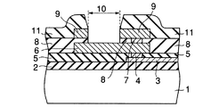
本実施の形態の半導体装置の構造を図1を用いて説明する。シリコンなどからなる半導体基板1上にTEOS等のシリコン酸化膜などからなる第1層間絶縁膜2が形成されている。この第1層間絶縁膜2上には、半導体基板上に形成されているトランジスタ(図示せず)に接続される内部配線3が形成されている。この内部配線3にはAl、Wなどの導電材料が用いられて形成される第1コンタクト4が接続されている。
【0022】
この第1コンタクト4の上、及び第1層間絶縁膜2の上には、第2層間絶縁膜5が形成されている。さらに、この第2層間絶縁膜5上には、ワイヤボンディング用電極パッド6が形成されている。このワイヤボンディング用電極パッド6は例えば、アルミニウム合金や銅合金などから形成されている。このワイヤボンディング用電極パッド6には、第1コンタクト4が接続されている。このようにして、ワイヤボンディング用電極パッド6は第1コンタクト4と内部配線3により、トランジスタなどの回路素子から形成される信号入出力回路や電源回路等に接続される。
【0023】
このワイヤボンディング用電極パッド6及び第2層間絶縁膜5上には、TEOSなどのシリコン酸化膜からなる厚さが例えば、約0.4μm程度の第3層間絶縁膜8が形成されている。この第3層間絶縁膜8中には、ワイヤボンディング用電極パッド6に接続するように第2コンタクト7がAl、Wなどの導電材料が用いられて形成されている。なお、第1コンタクト4及び第2コンタクト7はパッドと同様のアルミニウムなどの材料でもよい。
【0024】
この第2コンタクト7に接続され、第3層間絶縁膜8の上で、かつ、ワイヤボンディング用電極パッド6の直上にダイソート用電極パッド9が形成されている。このダイソート用電極パッド9は例えば、アルミニウム合金や銅合金などから形成されている。ダイソート用電極パッド9は、ワイヤボンディングを行うことがないので、ボンディングワイヤとの接合性を考慮する必要が無く、アルミ合金や銅合金以外にポリシリコン、タングステン、タングステンシリサイド、チタン、窒化チタンなどから適宜、選択的に使用することができる。
【0025】
このダイソート用電極パッド9には、開口部10が設けられ、その開口部10の大きさは例えば60μm四方の四角形で形成されている。また、このダイソート用電極パッド9の開口部10の真下の第3層間絶縁膜8中には、開口部10が設けられ、ワイヤボンディング用電極パッド6の上表面が露出している。
【0026】
ここで、ダイソート用電極パッド9及びワイヤボンディング用電極パッド6の厚さは例えば約1μm程度である。なお、ダイソート用電極パッド9の厚さはさらにより薄く設定してもよい、
さらに、第2層間絶縁膜5及びダイソート用電極パッド9の上には、シリコン窒化膜などから形成されるパッシベーション層11が形成されている。このパッシベーション層11においても、ダイソート用電極パッド9の開口部10の真上に開口部10が形成されている。ダイソート用電極パッド9の表面は開口部10以外では、パッシベーション層11により保護されている。
【0027】
ワイヤボンディング用電極パッド9の開口部10に露出した表面上には、金などから形成されたボンディングワイヤ12が接続されている。
【0028】
ダイソート用電極パッド9とワイヤボンディング用電極パッド6は、半導体基板1上の電極パッドの領域では開口して電極パッドとして機能するが、それ以外の領域では配線としても機能する。
【0029】
また、ダイソート用電極パッド9の大きさをワイヤボンディング用電極パッド6の大きさより小さく形成することで、ボンディング面の開口部を設ける際にワイヤボンディング用電極パッド6の下面と同一面の第2層間絶縁膜5が露出することを防止でき、半導体装置の信頼性向上に役に立つ。なお、ワイヤボンディング用電極パッド6は特に電源パッドとして使用する場合などには、より大きい形状としてもよい。
【0030】
本実施の形態によれば、ダイソート用電極パッドとワイヤボンディング用電極パッドを層構造とすることで半導体チップ表面における電極パッド領域の面積を小さくすることができ、半導体装置の高集積化を図ることができる。すなわち、従来例のようにダイソート用電極パッドとワイヤボンディング用電極パッドとを同一平面上に設けた場合と比べて、ダイソート用電極パッド分の面積を縮小することができる。
【0031】
また、センターパッド方式の半導体装置であっても、センターパッド領域に抵抗の増大無しにダイソート用電極パッドを設けることができ、さらに小面積のパッド領域を得ることができる。
【0032】
また、ダイソート用パッドの露出部は、ワイヤボンディング時には除去されている。このため、ダイソートを多数回繰り返して行って、ダイソート用パッド表面に多数の傷が生じていても、その傷が残ることがない。こうして、表面に凹凸が生じたパッドを持たない半導体装置を提供でき、半導体装置の信頼性を向上できる。
【0033】
次に、本実施の形態の半導体装置の製造方法を図1乃至図8を用いて説明する。
【0034】
図2に断面が示されるように、半導体基板1上にトランジスタ(図示せず)を設け、このトランジスタ上にTEOS膜などからなる第1層間絶縁膜2を設け、その第1層間絶縁膜2中にトランジスタに接続する内部配線3を設ける。
【0035】
さらに、この内部配線3上及び第1層間絶縁膜2上に第2層間絶縁膜5を設ける。さらに、この内部配線3に接続する第1コンタクト4を設ける。
【0036】
次に、この第1コンタクト4に接続して、例えばアルミニウム合金又は銅合金などからなるワイヤボンディング用電極パッド6を第2層間絶縁膜5上に設ける。
【0037】
このワイヤボンディング用電極パッド6及び第2層間絶縁膜5上にTEOS膜などからなる第3層間絶縁膜8を形成する。
【0038】
なお、ワイヤボンディング用電極パッド6に銅合金を使用した場合は、その表面には後の工程において接着されるボンディングワイヤとの接着性を増すためにアルミ二ウムを蒸着しておく。
【0039】
さらに、第3層間絶縁膜8中にワイヤボンディング用電極パッド6に接続する第2コンタクト7を形成する。さらに、この第2コンタクト7に接続させて、ワイヤボンディング用電極パッド6の真上の第3層間絶縁膜8上に、例えばアルミニウム合金又は銅合金などからなるダイソート用電極パッド9を形成する。
【0040】
さらに第3層間絶縁膜8上及びダイソート用電極パッド9上にパッシベーション層11を形成する。さらに、このパッシベーション層11の一部分を除去して開口部13を設けて、ダイソート用電極パッド9の上表面の一部を露出させる。
【0041】
ここでは、半導体基板は各半導体装置となる半導体チップとしては、まだ分割されておらず、半導体ウェハー状態となっている。
【0042】
次に、図3に示されるように、開口部13中で、金属製のダイソート用プローブ14をダイソート用電極パッド9に接触させ、半導体ウェハー状態でのダイソートを行なう。ダイソート用プローブ14と内部配線3は、ダイソート用電極パッド9、第2コンタクト7、ワイヤボンディング用電極パッド6、及び第1コンタクト4を介して電気的に接続されている。
【0043】
次に、図4には、半導体ウェハー状態でのダイソートが終了した段階での半導体装置の断面図が示される。ここでは、ダイソート用プローブ14をダイソート用電極パッド9から取り外した後の状態の断面が示されている。ダイソート用プローブ14を取り外した後の開口部13に露出したダイソート用電極パッド9には傷16が生じている。図4に示されるように傷16が深く形成された場合、第3層間絶縁膜8が露出した状態となっている。
【0044】
さらに傷が深く形成されて、第3層間絶縁膜8中にまで達した場合であっても、後の工程で、当該部分の第3層間絶縁膜8は除去されるので、問題とはならない。
【0045】
次に、図5には、マスク材15を塗布した状態の半導体装置の断面が示される。このマスク材15は感光性レジスト等が使用される。i線等の光源によりダイソート用電極パッド9の開口部13の位置に合わせて、マスク材15がパターニングされる。この時、傷16にマスク材15が残らないように後処理をする。ここで、傷16にマスク材15が残らないように後処理を行うのは、次のアッシャー工程におけるRIE(Reactive Ion Etching)において、マスク材15の残部で不均一なエッチングが行われてしまい、開口部に露出する第3層間絶縁膜8の上表面に凹凸が生じることを防止するためである。
【0046】
次に、図6に示されるように半導体ウェハー表面からCDE(Chemical Dry Etching)、またはRIEのエッチングを行い、ダイソート用電極パッド9に開口部10を設ける。この際、第3層間絶縁膜8の表面はエッチングによりダメージがあるが、その下にあるワイヤボンディング用電極パッド6にはダメージは到達しない。このようにワイヤボンディング用電極パッド6にダメージが到達しないことで、後の工程におけるボンディングワイヤとの良好なボンディング性を維持できる。
【0047】
この工程では、ダイソート用電極パッド9のエッチングが少々オーバー気味に行なわれた場合でも、その下方にある第3層間絶縁膜8を除去することがない。すなわち、使用する薬品と処理方法を変えることで、ダイソート用電極パッド9と第3層間絶縁膜8とを別々に除去することができる。なお、この工程において、ダイソートパッド全体を除去するのではなく、一部分のみを除去することで、開口をエッチングする際のばらつきなどによる周囲部分への影響を無くすことができる。
【0048】
次に、図7に示されるようにレジスト15をマスクとして、開口部10に露出した第3層間絶縁膜8をCDE、又はRIEのエッチングを行って取り除く。こうして、ワイヤボンディング用電極パッド6の上表面の一部が露出する。このとき、ワイヤボンディング用電極パッド6は、エッチングにより若干のダメージがあるが、それにより表面には第3層間絶縁膜8が残っていない状態となる。ここで、形成されるワイヤボンディング用電極パッド6の開口部10の大きさは、図2で形成されるダイソート用電極パッド9の開口部13の大きさよりも大きいことが好ましい。このような開口部の大小関係を持たせることで、ダイソート用電極パッド9に生じたダイソート用プローブ14による損傷部16を完全に除去することができる。
【0049】
この工程においては、ボンディング用電極パッド6表面のエッチングダメージの制御は、RIEを用いた場合、使用する混合雰囲気の濃度とエッチング時間を調整して行なう。また、CDEを用いた場合、使用する薬液濃度とエッチング時間を調整して行う。また、第3層間絶縁膜8のエッチングの際には、少々オーバー気味にエッチングが行なわれてもボンディング用電極パッド6を溶かすことがないので、最終的にボンディング用電極パッド6の表面がダメージなく露出する。
【0050】
なお、ボンディング用電極パッド6まで傷16が到達してしまった場合、その表面をエッチングする際に、その傷16を無くす程度までエッチングを進めると傷を残さなくすることも可能である。
【0051】
ここで、ワイヤボンディング用電極パッド6の上に部分的に第3層間絶縁膜8が残っていると、絶縁膜が後の工程で接着するボンディングワイヤとワイヤボンディング用電極パッド6との間に介在することになり、ボンディング特性がきわだって低下する。このような状態が生じるのを防ぐため、例えば、約0.1μm程度の深さで余分にワイヤボンディング用電極パッド6の上表面を除去する。
【0052】
次に、図8に示されるようにマスク材15を除去して、パッシベーション層11の上表面を露出させる。
【0053】
次に、半導体ウェハーに複数個形成された半導体装置を個別にダイシングを施して、分離した後で、図1に示すようにワイヤボンディング用電極パッド6に例えば金からなるボンディングワイヤ12を接続する。ワイヤボンディング用電極パッド6とボンディングワイヤ12とは良好な接合をしている。すなわち、ダイソート用電極パッド9とワイヤボンディング用電極パッド6を分離して、配置することで、ダイソート用プローブ14がダイソート用電極パッド9に接触するときに生ずる傷16がワイヤボンディング用電極パッド6に影響を与えない。すなわち、ダイソート用電極パッド9とワイヤボンディング用電極パッド6とを分離して設けることで、ダイソート用プローブ14の接触による電極パッドの傷があってもワイヤボンディング性に影響を与えない効果を得ることができる。
【0054】
また、ダイソート用電極パッド9とワイヤボンディング用電極パッド6とを同一平面上に配置するのではなく、上下方向の層構造として配置することで、半導体装置に占める電極パッド領域の割合を小さくできる。
【0055】
ここで、金からなるボンディングワイヤ12が用いられ、アルミニウムからなるワイヤボンディング用電極パッド6が用いられた場合、ワイヤボンディング用電極パッド6のボンディングワイヤ12との接触面には、アルミニウムと金との合金層が形成される。
【0056】
なお、パッシベーション層11とダイソート用電極パッド9との間、ダイソート用電極パッド9と第3層間絶縁膜8との間、ワイヤボンディング電極パッド6と第2層間絶縁膜5との間にそれぞれ、開口部を設けるエッチング工程の際にコロージョンが発生する可能性が見込まれる場合には、開口部に露出する側面をシリコン窒化膜などの保護膜で覆うことで、信頼性を向上することができる。この保護膜は図6に示される工程において、開口部10を形成した後に露出面上にシリコン窒化膜を堆積する。さらに図7に示される工程において、第3層間絶縁膜8上に形成されたシリコン窒化膜を第3層間絶縁膜8とともに除去して、ボンディング用電極パッド6の上表面を露出することで、工程数の増加を最小限に抑制して、形成することができる。
【0057】
また、ワイヤボンディング用電極パッド6に接着されたボンディングワイヤ12が露出しているダイソート用電極パッド9の側面に接触するような状況が生じても、ダイソート用電極パッド9、ワイヤボンディング用電極パッド6、及びボンディングワイヤ12は同一電位であるので、その特性上の問題はない。
【0058】
なお、図6に示された工程において、ダイソート用電極パッド9やダイソート用電極パッド9とボンディング用電極パッド6との間の第2コンタクト7をすべて除去して、ボンディング用電極パッド6の開口部10をより大きく形成することもできる。
【0059】
さらに図6の工程において、ダイソート用電極パッド9やダイソート用電極パッド9とボンディング用電極パッド6との間の第2コンタクト7をすべて除去して、開口部10の位置をダイソート用の開口部13の位置と異ならせて、図6中でより右寄りに設けることもできる。
【0060】
なお、図1で形成されたダイソート用電極パッド9は、すべてのパッドについてダイソートテストを行なう必要がなく、ダイソート用プローブ14をすべてのダイソート用電極パッド9に接触しなくてもよい。そのようなダイソート用電極パッド9には、ダイソート用プローブ14の接触による傷が表面に生じることはない。
【0061】
本実施の形態によれば、ダイソート用電極パッドとワイヤボンディング用電極パッドを層構造とすることで半導体チップ表面における電極パッド領域の面積を小さくすることができ、高集積化された半導体装置の製造方法を提供できる。すなわち、従来例のようにダイソート用電極パッドとワイヤボンディング用電極パッドとを同一平面上に設けた場合と比べて、ダイソート用電極パッド分の面積を縮小した半導体装置の製造方法を提供することができる。
【0062】
また、ダイソート用電極パッド9の露出部は、ワイヤボンディング時には除去されている。このため、ダイソートテストを多数回繰り返して行って、ダイソート用電極パッド9表面に多数の傷16が生じていても、その傷16が残ることがない。こうして、表面に凹凸が生じたワイヤボンディング用電極パッド6を持たない信頼性の高い半導体装置の製造方法を提供できる。
【0063】
【発明の効果】
本発明によれば、電極パッド領域の面積を増加させずにボンディングワイヤとワイヤボンディング用電極パッドの電気特性を向上させた半導体装置及びその製造方法を提供できる。
【図面の簡単な説明】
【図1】 本発明の実施の形態の半導体装置の断面図。
【図2】 本発明の実施の形態の半導体装置の製造方法の一工程を表す断面図。
【図3】 本発明の実施の形態の半導体装置の製造方法の一工程を表す断面図。
【図4】 本発明の実施の形態の半導体装置の製造方法の一工程を表す断面図。
【図5】 本発明の実施の形態の半導体装置の製造方法の一工程を表す断面図。
【図6】 本発明の実施の形態の半導体装置の製造方法の一工程を表す断面図。
【図7】 本発明の実施の形態の半導体装置の製造方法の一工程を表す断面図。
【図8】 本発明の実施の形態の半導体装置の製造方法の一工程を表す断面図。
【図9】 (A)は、従来の第1の技術の半導体装置の電極パッド周辺のワイヤボンディング前の状態を表す断面図であり、(B)は、従来の第1の技術の半導体装置の電極パッド周辺のワイヤボンディング後の状態を表す断面図である。
【図10】 (A)は、従来の第1の技術の半導体装置の電極パッド周辺のダイソートテストを行なっている状態を表す断面図であり、(B)は、従来の第1の技術の半導体装置の電極パッド周辺のダイソートテスト後のワイヤボンディング後の状態を表す断面図である。
【図11】 従来の第2の技術の半導体装置の電極パッド周辺を表す断面図。
【図12】 (A)は、従来の第3の技術の半導体装置の電極パッド周辺を表す断面図であり、(B)は、従来の第3の技術の半導体装置の電極パッド周辺を表す上面図である。
【図13】 (A)は、従来の第4の技術の半導体装置の電極パッド周辺を表す断面図であり、(B)は、従来の第4の技術の半導体装置の電極パッド周辺を表す上面図である。
【符号の説明】
1 半導体基板
2 第1層間絶縁膜
3 内部配線
4 第1コンタクト
5 第2層間絶縁膜
6 ワイヤボンディング用電極パッド
7 第2コンタクト
8 第3層間絶縁膜
9 ダイソート用電極パッド
10,13 開口部
11 パッシベーション層
12 ボンディングワイヤ
14 ダイソート用プローブ
15 マスク材
16 傷[0001]
BACKGROUND OF THE INVENTION
The present invention relates to a semiconductor device including an electrode pad, and more particularly to a semiconductor device including a die sort electrode pad and a wire bonding electrode pad and a manufacturing method thereof.
[0002]
[Prior art]
A conventional wire bonding method for a semiconductor device having a bonding pad will be described with reference to FIG.
[0003]
FIG. 9A shows a cross section of the semiconductor device around the bonding pad before wire bonding is performed. As shown in FIG. 9A, a first interlayer
[0004]
Usually, a semiconductor device performs a die sort test in which defective products are screened at a wafer level after completing a manufacturing process in a semiconductor wafer state and before package assembly.
[0005]
FIG. 9B shows a state in which wire bonding is performed without performing this die sort test. A
[0006]
Next, the structure of the semiconductor device around the wire bonding electrode pad when the die sort test is performed will be described with reference to FIG. FIG. 10A shows a cross section in the state of the die sort test. Die sorting is performed by bringing a metal
[0007]
After performing the die sort test, the
[0008]
In order to solve this problem, conventionally, a countermeasure as shown in FIG. 11 has been proposed. FIG. 11 shows a technique described in Japanese Patent Laid-Open No. 62-261139. A
[0009]
There is also a proposal described in JP-A-11-87441 as shown in FIGS. FIG. 12A shows a cross-sectional structure of the first type of electrode pad, and FIG. 12B shows a top view of the electrode pad. In this way, the same electrode pad is divided into the
[0010]
FIG. 13A shows a cross-sectional structure of a second type of electrode pad, and FIG. 13B shows a top view of the electrode pad. In this way, adjacent electrode pads are connected by the
[0011]
With these methods, the effect of scratches caused by the die sort probe during die sort is prevented from affecting the pad electrode bonded to the bonding wire.
[0012]
[Problems to be solved by the invention]
The conventional semiconductor device as described above has the following problems.
[0013]
In the method shown in FIG. 11, when the needle pad area of the scribe line and the electrode pad for wire bonding are separated, for example, when there is an electrode pad at the center of the chip, wiring for connecting the scribe line and the electrode pad is not routed. It becomes difficult. In addition, the extension of the wiring connecting the scribe line and the electrode pad has a drawback of increasing the resistance value and deteriorating the circuit characteristics. In particular, in a high-frequency semiconductor device, a long wiring length increases resistance and causes a problem in characteristics.
[0014]
Further, in the method shown in FIG. 12 or FIG. 13, the area of the electrode pad is increased, an obstacle to the reduction of the semiconductor chip, and the wiring from the electrode pad to the peripheral circuit becomes longer, thereby deteriorating the circuit characteristics. There was a factor.
[0015]
An object of the present invention is to solve the above-described problems of the prior art.
[0016]
In particular, an object of the present invention is to provide a semiconductor device and a manufacturing method thereof in which the electrical characteristics of the bonding wire and the wire bonding electrode pad are improved without increasing the area of the electrode pad region.
[0017]
[Means for Solving the Problems]
To achieve the above objectiveThe semiconductor device of one embodiment of the present invention includes:A semiconductor substrate, a first interlayer insulating film provided on the semiconductor substrate, a wiring layer provided in a part on the first interlayer insulating film, and on the first interlayer insulating film and the wiring layer; A second interlayer insulating film provided; a first electrode pad formed through the second interlayer insulating film and connected to the wiring layer; the first electrode pad; and the second interlayer insulating film Provided on theAn opening for exposing the surface of the first electrode pad is provided in a part thereof.A third interlayer insulating film, and the third interlayer insulating film,An opening is formed on the opening of the third interlayer insulating film.Formed on the second electrode pad, the second electrode pad and the third interlayer insulating film;An opening is provided on the opening of the second electrode pad.A passivation layer is provided.
[0018]
In addition, a semiconductor device according to another aspect of the present invention includes:A semiconductor substrate having a circuit element formed on the surface thereof; a first interlayer insulating film formed on the semiconductor substrate; an internal wiring layer formed on the first interlayer insulating film and connected to the circuit element; A second interlayer insulating film formed on the internal wiring layer and the first interlayer insulating film, a wire bonding electrode pad formed on the second interlayer insulating film, and the wire bonding electrode pad; A first contact connecting the internal wiring layer, a third interlayer insulating film formed on the wire bonding electrode pad, and formed on the wire bonding electrode pad via the third interlayer insulating film An electrode pad for die sorting, and a second contact connected between the electrode pad for die sorting and the electrode pad for wire bonding,The die sort electrode pad has an opening in a part thereof, an opening is provided in the third interlayer insulating film below the opening, and the wire bonding electrode pad surface is exposed in the opening of the third interlayer insulating film. It is characterized by that.
[0019]
In addition, a semiconductor device according to another aspect of the present invention includes:A semiconductor substrate, a first interlayer insulating film provided on the semiconductor substrate, a wiring layer provided in a part on the first interlayer insulating film, and on the first interlayer insulating film and the wiring layer; A second interlayer insulating film provided; a first electrode pad formed through the second interlayer insulating film and connected to the wiring layer; the first electrode pad; and the second interlayer insulating film Provided on theAn opening for exposing the surface of the first electrode pad is provided in a part thereof.A third interlayer insulating film, and the third interlayer insulating film,An opening is formed on the opening of the third interlayer insulating film.Formed on the second electrode pad, the second electrode pad and the third interlayer insulating film;An opening is provided on the opening of the second electrode pad.A passivation layer,At least part of the exposed surface of the first electrode padIt comprises a bonding wire that is wire-bonded.
[0020]
A method for manufacturing a semiconductor device according to another aspect of the present invention includes:Forming a first interlayer insulating film on the semiconductor substrate; forming an internal wiring on the first interlayer insulating film; and forming a second interlayer insulating film on the internal wiring and on the first interlayer insulating film. A step of forming, a step of forming a first electrode pad connected to the internal wiring on the second interlayer insulating film, and a third interlayer insulating film on the first electrode pad and the second interlayer insulating film Forming a second electrode pad connected to the first electrode pad on the third interlayer insulating film, and a passivation layer on the second electrode pad and on the third interlayer insulating film. Forming an opening so as to expose at least a part of the surface of the passivation layer on the second electrode pad, applying a probe to the second electrode pad exposed in the opening, To test Removing the exposed second electrode pad and the third interlayer insulating film below the exposed second electrode pad to expose the upper surface of the first electrode pad; and A step of wire bonding a bonding wire to the upper surface of the first electrode pad is provided.
[0021]
DETAILED DESCRIPTION OF THE INVENTION
The structure of the semiconductor device of this embodiment will be described with reference to FIG. A first
[0022]
A second
[0023]
On the wire
[0024]
A die
[0025]
The die
[0026]
Here, the thicknesses of the die
Further, a
[0027]
A
[0028]
The die
[0029]
Further, by forming the die
[0030]
According to the present embodiment, the area of the electrode pad region on the surface of the semiconductor chip can be reduced by forming the electrode pad for die sorting and the electrode pad for wire bonding into a layer structure, thereby achieving high integration of the semiconductor device. Can do. That is, the area of the die sort electrode pad can be reduced as compared with the case where the die sort electrode pad and the wire bonding electrode pad are provided on the same plane as in the conventional example.
[0031]
Even in a center pad type semiconductor device, a die sort electrode pad can be provided in the center pad region without an increase in resistance, and a pad region with a smaller area can be obtained.
[0032]
The exposed portion of the die sort pad is removed during wire bonding. For this reason, even if the die sort is repeated many times and many scratches are generated on the die sort pad surface, the scratches will not remain. Thus, it is possible to provide a semiconductor device that does not have a pad with unevenness on the surface, and the reliability of the semiconductor device can be improved.
[0033]
Next, a method for manufacturing the semiconductor device of this embodiment will be described with reference to FIGS.
[0034]
As shown in FIG. 2, a transistor (not shown) is provided on the
[0035]
Further, a second
[0036]
Next, an
[0037]
A third
[0038]
In the case where a copper alloy is used for the wire
[0039]
Further, a
[0040]
Further, a
[0041]
Here, the semiconductor substrate is not yet divided as a semiconductor chip to be each semiconductor device, and is in a semiconductor wafer state.
[0042]
Next, as shown in FIG. 3, a metal
[0043]
Next, FIG. 4 shows a cross-sectional view of the semiconductor device at the stage where die sort in the semiconductor wafer state is completed. Here, a cross section of the state after the
[0044]
Even when the scratches are deeply formed and reach the third
[0045]
Next, FIG. 5 shows a cross section of the semiconductor device with the
[0046]
Next, as shown in FIG. 6, CDE (Chemical Dry Etching) or RIE etching is performed from the surface of the semiconductor wafer to provide an
[0047]
In this step, even if the die
[0048]
Next, as shown in FIG. 7, using the resist 15 as a mask, the third
[0049]
In this step, the etching damage on the surface of the
[0050]
When the
[0051]
Here, if the third
[0052]
Next, as shown in FIG. 8, the
[0053]
Next, a plurality of semiconductor devices formed on the semiconductor wafer are individually diced and separated, and then bonding
[0054]
Further, the die
[0055]
Here, when the
[0056]
Openings are provided between the
[0057]
Even when the
[0058]
In the step shown in FIG. 6, all of the die
[0059]
Further, in the step of FIG. 6, the die
[0060]
The die
[0061]
According to the present embodiment, the area of the electrode pad region on the surface of the semiconductor chip can be reduced by forming the electrode pad for die sorting and the electrode pad for wire bonding in a layered structure, and manufacturing a highly integrated semiconductor device Can provide a method. That is, it is possible to provide a method of manufacturing a semiconductor device in which the area of the die sort electrode pad is reduced as compared with the case where the die sort electrode pad and the wire bonding electrode pad are provided on the same plane as in the conventional example. it can.
[0062]
The exposed portion of the die
[0063]
【The invention's effect】
ADVANTAGE OF THE INVENTION According to this invention, the semiconductor device which improved the electrical characteristic of the bonding wire and the electrode pad for wire bonding, and its manufacturing method can be provided, without increasing the area of an electrode pad area | region.
[Brief description of the drawings]
FIG. 1 is a cross-sectional view of a semiconductor device according to an embodiment of the present invention.
FIG. 2 is a cross-sectional view illustrating a step of a method for manufacturing a semiconductor device according to an embodiment of the present invention.
FIG. 3 is a cross-sectional view illustrating a process of a method for manufacturing a semiconductor device according to an embodiment of the present invention.
FIG. 4 is a cross-sectional view illustrating a step of a method for manufacturing a semiconductor device according to an embodiment of the present invention.
FIG. 5 is a cross-sectional view illustrating a step of the method of manufacturing a semiconductor device according to the embodiment of the present invention.
FIG. 6 is a cross-sectional view illustrating a step of the method of manufacturing a semiconductor device according to the embodiment of the present invention.
FIG. 7 is a cross-sectional view illustrating a step of the method of manufacturing a semiconductor device according to the embodiment of the present invention.
FIG. 8 is a cross-sectional view illustrating a step of the method of manufacturing a semiconductor device according to the embodiment of the present invention.
9A is a cross-sectional view showing a state before wire bonding around an electrode pad of a conventional semiconductor device of the first technology, and FIG. 9B is a cross-sectional view of the conventional semiconductor device of the first technology. It is sectional drawing showing the state after wire bonding around an electrode pad.
FIG. 10A is a cross-sectional view showing a state in which a die sort test is performed around the electrode pad of the semiconductor device of the conventional first technique, and FIG. 10B is a diagram of the conventional first technique. It is sectional drawing showing the state after the wire bonding after the die sort test of the electrode pad periphery of a semiconductor device.
FIG. 11 is a sectional view showing the periphery of an electrode pad of a semiconductor device according to a second conventional technique.
12A is a cross-sectional view illustrating the periphery of an electrode pad of a semiconductor device according to a third conventional technique, and FIG. 12B is a top view illustrating the periphery of the electrode pad of a semiconductor device according to a third conventional technique. FIG.
13A is a cross-sectional view illustrating the periphery of an electrode pad of a semiconductor device according to a fourth conventional technique, and FIG. 13B is a top view illustrating the periphery of the electrode pad of a semiconductor device according to a fourth conventional technique. FIG.
[Explanation of symbols]
1 Semiconductor substrate
2 First interlayer insulating film
3 Internal wiring
4 First contact
5 Second interlayer insulating film
6 Electrode pads for wire bonding
7 Second contact
8 Third interlayer insulating film
9 Die sort electrode pads
10,13 opening
11 Passivation layer
12 Bonding wire
14 Probe for die sort
15 Mask material
16 wounds
Claims (7)
Priority Applications (1)
| Application Number | Priority Date | Filing Date | Title |
|---|---|---|---|
| JP2001271255A JP3856426B2 (en) | 2001-09-07 | 2001-09-07 | Semiconductor device and manufacturing method thereof |
Applications Claiming Priority (1)
| Application Number | Priority Date | Filing Date | Title |
|---|---|---|---|
| JP2001271255A JP3856426B2 (en) | 2001-09-07 | 2001-09-07 | Semiconductor device and manufacturing method thereof |
Publications (2)
| Publication Number | Publication Date |
|---|---|
| JP2003086624A JP2003086624A (en) | 2003-03-20 |
| JP3856426B2 true JP3856426B2 (en) | 2006-12-13 |
Family
ID=19096785
Family Applications (1)
| Application Number | Title | Priority Date | Filing Date |
|---|---|---|---|
| JP2001271255A Expired - Fee Related JP3856426B2 (en) | 2001-09-07 | 2001-09-07 | Semiconductor device and manufacturing method thereof |
Country Status (1)
| Country | Link |
|---|---|
| JP (1) | JP3856426B2 (en) |
Families Citing this family (1)
| Publication number | Priority date | Publication date | Assignee | Title |
|---|---|---|---|---|
| JP5401817B2 (en) | 2008-03-25 | 2014-01-29 | 富士通セミコンダクター株式会社 | Semiconductor device manufacturing method and semiconductor device |
-
2001
- 2001-09-07 JP JP2001271255A patent/JP3856426B2/en not_active Expired - Fee Related
Also Published As
| Publication number | Publication date |
|---|---|
| JP2003086624A (en) | 2003-03-20 |
Similar Documents
| Publication | Publication Date | Title |
|---|---|---|
| JP3616444B2 (en) | Semiconductor device | |
| KR100329407B1 (en) | Electrode structure of semiconductor element | |
| US7105917B2 (en) | Semiconductor device having a fuse connected to a pad and fabrication method thereof | |
| US20060267222A1 (en) | Semiconductor element and manufacturing method thereof | |
| JP2006210438A (en) | Semiconductor device and its manufacturing method | |
| US7429795B2 (en) | Bond pad structure | |
| JP3468188B2 (en) | Semiconductor device and its manufacturing method. | |
| TWI316741B (en) | Method for forming an integrated cricuit, method for forming a bonding pad in an integrated circuit and an integrated circuit structure | |
| US20070290204A1 (en) | Semiconductor structure and method for manufacturing thereof | |
| US9941236B2 (en) | Semiconductor device having wire bonding connection and method for manufacturing the same | |
| US20060180945A1 (en) | Forming a cap above a metal layer | |
| JPH09289224A (en) | Semiconductor chip, manufacturing method thereof and wire bonding method | |
| JP3856426B2 (en) | Semiconductor device and manufacturing method thereof | |
| KR20060078864A (en) | Semiconductor device and method for fabricating the same | |
| JP3599813B2 (en) | Semiconductor device | |
| JP3395747B2 (en) | Manufacturing method of semiconductor integrated circuit | |
| US20090014717A1 (en) | Test ic structure | |
| JP2949830B2 (en) | Failure analysis method for semiconductor device | |
| KR100339414B1 (en) | Forming method of pad using semiconductor power line analsis | |
| KR20040023311A (en) | Method for forming pad of semiconductor drvice | |
| KR100481832B1 (en) | Method for forming a semiconductor device and a semiconductor formed thereof | |
| JP2002373909A (en) | Semiconductor circuit device and manufacturing method therefor | |
| KR20010017176A (en) | method for manufacturing semiconductor devices | |
| KR20030061158A (en) | Semiconductor device having bonding pads and method of fabricating the same | |
| KR20040057516A (en) | Method for forming a bonding pad in semiconductor device |
Legal Events
| Date | Code | Title | Description |
|---|---|---|---|
| A621 | Written request for application examination |
Free format text: JAPANESE INTERMEDIATE CODE: A621 Effective date: 20050401 |
|
| RD02 | Notification of acceptance of power of attorney |
Free format text: JAPANESE INTERMEDIATE CODE: A7422 Effective date: 20050428 |
|
| RD04 | Notification of resignation of power of attorney |
Free format text: JAPANESE INTERMEDIATE CODE: A7424 Effective date: 20050606 |
|
| A977 | Report on retrieval |
Free format text: JAPANESE INTERMEDIATE CODE: A971007 Effective date: 20060607 |
|
| A131 | Notification of reasons for refusal |
Free format text: JAPANESE INTERMEDIATE CODE: A131 Effective date: 20060613 |
|
| A521 | Written amendment |
Free format text: JAPANESE INTERMEDIATE CODE: A523 Effective date: 20060809 |
|
| TRDD | Decision of grant or rejection written | ||
| A01 | Written decision to grant a patent or to grant a registration (utility model) |
Free format text: JAPANESE INTERMEDIATE CODE: A01 Effective date: 20060908 |
|
| A61 | First payment of annual fees (during grant procedure) |
Free format text: JAPANESE INTERMEDIATE CODE: A61 Effective date: 20060911 |
|
| R150 | Certificate of patent or registration of utility model |
Free format text: JAPANESE INTERMEDIATE CODE: R150 |
|
| FPAY | Renewal fee payment (event date is renewal date of database) |
Free format text: PAYMENT UNTIL: 20090922 Year of fee payment: 3 |
|
| FPAY | Renewal fee payment (event date is renewal date of database) |
Free format text: PAYMENT UNTIL: 20100922 Year of fee payment: 4 |
|
| FPAY | Renewal fee payment (event date is renewal date of database) |
Free format text: PAYMENT UNTIL: 20110922 Year of fee payment: 5 |
|
| LAPS | Cancellation because of no payment of annual fees |