JP3793507B2 - Content, addressable, magnetic random access memory - Google Patents
Content, addressable, magnetic random access memory Download PDFInfo
- Publication number
- JP3793507B2 JP3793507B2 JP2002561835A JP2002561835A JP3793507B2 JP 3793507 B2 JP3793507 B2 JP 3793507B2 JP 2002561835 A JP2002561835 A JP 2002561835A JP 2002561835 A JP2002561835 A JP 2002561835A JP 3793507 B2 JP3793507 B2 JP 3793507B2
- Authority
- JP
- Japan
- Prior art keywords
- transistor
- line
- match
- contact
- control terminal
- Prior art date
- Legal status (The legal status is an assumption and is not a legal conclusion. Google has not performed a legal analysis and makes no representation as to the accuracy of the status listed.)
- Expired - Fee Related
Links
Images


Classifications
-
- G—PHYSICS
- G11—INFORMATION STORAGE
- G11C—STATIC STORES
- G11C11/00—Digital stores characterised by the use of particular electric or magnetic storage elements; Storage elements therefor
- G11C11/02—Digital stores characterised by the use of particular electric or magnetic storage elements; Storage elements therefor using magnetic elements
- G11C11/14—Digital stores characterised by the use of particular electric or magnetic storage elements; Storage elements therefor using magnetic elements using thin-film elements
- G11C11/15—Digital stores characterised by the use of particular electric or magnetic storage elements; Storage elements therefor using magnetic elements using thin-film elements using multiple magnetic layers
-
- G—PHYSICS
- G11—INFORMATION STORAGE
- G11C—STATIC STORES
- G11C15/00—Digital stores in which information comprising one or more characteristic parts is written into the store and in which information is read-out by searching for one or more of these characteristic parts, i.e. associative or content-addressed stores
- G11C15/04—Digital stores in which information comprising one or more characteristic parts is written into the store and in which information is read-out by searching for one or more of these characteristic parts, i.e. associative or content-addressed stores using semiconductor elements
- G11C15/046—Digital stores in which information comprising one or more characteristic parts is written into the store and in which information is read-out by searching for one or more of these characteristic parts, i.e. associative or content-addressed stores using semiconductor elements using non-volatile storage elements
-
- G—PHYSICS
- G11—INFORMATION STORAGE
- G11C—STATIC STORES
- G11C15/00—Digital stores in which information comprising one or more characteristic parts is written into the store and in which information is read-out by searching for one or more of these characteristic parts, i.e. associative or content-addressed stores
- G11C15/02—Digital stores in which information comprising one or more characteristic parts is written into the store and in which information is read-out by searching for one or more of these characteristic parts, i.e. associative or content-addressed stores using magnetic elements
Description
本発明はコンピュータメモリに関し、特にキャッシュメモリ等に関するものである。 The present invention relates to computer memory, and more particularly to cache memory and the like.
コンピュータでは、キャッシュメモリは直近にアクセスされたコードまたはデータを保持する中央演算装置(CPU)に近接して配置される高速メモリである。データがキャッシュ内に無いとキャッシュミスが生じ、データがメインメモリから読み出されてキャッシュに収められる。この間、CPUは中断させられ、データが使用できるようになるまで待ち状態に置かれる。 In a computer, the cache memory is a high-speed memory that is placed in close proximity to a central processing unit (CPU) that holds the most recently accessed code or data. If the data is not in the cache, a cache miss occurs and the data is read from the main memory and stored in the cache. During this time, the CPU is suspended and placed in a wait state until data is available.
CPUはキャッシュにアドレスを送信し、キャッシュに保存されるワードを含むキャッシュを確認する。各セルに保存されるデータは一括して「タグ」と呼ばれ、タグワードは一行のタグまたはメモリセルから形成される。CPUにより指定されるワードがキャッシュ内にある場合、そのワードはキャッシュから読み出される。ワードがキャッシュ内に無い場合、メインメモリを指定してそのワードを読み出す。次に、丁度今アクセスされたワードを含む一ブロックのワードがメインメモリからキャッシュに転送される。 The CPU sends the address to the cache and checks the cache containing the words stored in the cache. Data stored in each cell is collectively referred to as a “tag”, and a tag word is formed from a single row of tags or memory cells. If the word specified by the CPU is in the cache, the word is read from the cache. If the word is not in the cache, the main memory is specified and the word is read. Next, a block of words, including the word just accessed, is transferred from main memory to the cache.
キャッシュメモリはCPUからアドレスを受信し、検索を行ってキャッシュに保存されているアドレスを比較する。この比較を並列に高速で行うためには、連想メモリすなわちコンテント・アドレッサブル(内容照合)・メモリ(CAM)が必要となる。メモリ内情報へのアクセス時間は、保存データがアドレスではなくむしろ内容により特定され得るのであれば、大きく減らすことができる。CAMまたは関連メモリは、特にキャッシュメモリ及び変換索引バッファにおいて使用される(TLB)。一般的に、CAMをキャッシュ内で用いて物理アドレスをデータに変換し、かつ、TLB内で用いて仮想アドレスを物理アドレスに変換する。CAMは関連データ処理にとって非常に強力なツールである。 The cache memory receives addresses from the CPU, performs a search, and compares the addresses stored in the cache. In order to perform this comparison in parallel at high speed, an associative memory, that is, a content addressable memory (CAM), is required. Access time to in-memory information can be greatly reduced if the stored data can be specified by content rather than by address. CAM or associated memory is used in particular in cache memory and translation index buffers (TLB). In general, a CAM is used in a cache to convert a physical address to data, and a TLB is used to convert a virtual address to a physical address. CAM is a very powerful tool for related data processing.
速度はキャッシュメモリにとって重要である。というのは、一般的に、キャッシュメモリはメインメモリよりも5〜10倍速くなければならないからである。今日まで、SRAMだけがキャッシュメモリなどが必要とする速度を有している。 Speed is important for cache memory. This is because, in general, cache memory must be 5 to 10 times faster than main memory. To date, only SRAM has the speed required by cache memory and the like.
先行技術においては、ほとんどのキャッシュメモリはSRAMアレイからなる。SRAM型のメモリセルは要求される速度を有するが、それらは揮発性メモリである。先行技術においてはSRAMセルはアレイ状に形成され、すべての比較及び一致検出回路がアレイの周辺または外側に配置される。また、SRAMをベースとするCAMはセルの位置ではターンオフさせることができず、周辺でマスキングしなければならず、結果として電力を浪費する。さらに、一般的に、メインメモリでは異なるメモリセルが使用され、キャッシュメモリ及びメインメモリは異なる処理及び製造工程を必要とする。 In the prior art, most cache memories consist of SRAM arrays. Although SRAM type memory cells have the required speed, they are volatile memory. In the prior art, SRAM cells are formed in an array, and all comparison and match detection circuits are located at the periphery or outside of the array. Also, the SRAM-based CAM cannot be turned off at the cell location and must be masked around, resulting in wasted power. Further, generally, different memory cells are used in the main memory, and the cache memory and the main memory require different processing and manufacturing processes.
従って、これらの問題を解決するキャッシュメモリを提供することが強く望まれている。 Accordingly, it is highly desirable to provide a cache memory that solves these problems.
次に、図1に本発明によるコンテント・アドレッサブル磁気ランダムメモリセル10を示す。セル10は差動接続された対(differentially connected pair)をなす磁気トンネル接合(MTJ)12,14を含む。MTJは回路内で接続して使用するが、回路内で接続することにより、電気がある磁性層から別の磁性層にMTJを形成する積層を垂直に通って流れる。MTJは電気的には抵抗器として表わすこ
とができ、その抵抗の大きさは双安定状態のいずれかにおける2つの磁気ベクトルの向きに依存する。この技術分野の当業者には明らかなように、MTJは磁気ベクトルが揃わない(互いに反対方向を指す)場合に比較的大きな抵抗を示し、磁気ベクトルが揃う場合に比較的小さな抵抗を示す。MTJはこの技術分野では良く知られているところであり、ここでは詳細には議論しない。しかしながら、MTJの製造方法及び動作に関してさらに情報を得たい場合は、「多層磁気トンネル接合メモリセル(Multi−Layer Magnetic Tunneling Junction Memory Cells)」と題する、1998年3月31日発行の米国特許第5,702,831号を参照されたい。この公報は、それを参照することにより本発明の開示に援用される。
Next, FIG. 1 shows a content addressable magnetic
セル10はさらに比較及び一致検出回路15を含み、この回路は差動接続された対をなすMTJ12,14に接続される。回路15は、BL及びBLN(反転ビットライン)と表示される差動タグビットライン、PBL及びPBLNと表示される差動タグプログラムビットライン、ELと表示されるイネーブルライン、WLと表示されるワードライン、DLと表示されるデジットライン、及びMLと表示されるマッチラインを含み、マッチラインMLは差動タグビットライン経由の入力データとセルに保存されるデータとの間の一致を表示する。
特に、MTJ12の(図1における)下側端子16はタグプログラムビットラインPBLに直接接続され、MTJ14の(図1における)下側端子17は反転タグプログラムビットラインPBLNに直接接続される。今ここに以下に詳細に説明する理由により、MTJ12,14の下側端子16,17は積層構造の頂部に位置し、この積層構造はMTJを形成し、上側端子18及び19はそれぞれ積層構造の底面に位置する。MTJ12の上側端子18は、第1スイッチングトランジスタ21及び第2スイッチングトランジスタ22を通して接点24に接続される。MTJ14の上側端子19は、第1スイッチングトランジスタ25及び第2スイッチングトランジスタ26を通して接点27に接続される。スイッチングトランジスタ21,25の制御端子またはゲートはイネーブルラインELに直接接続される。スイッチングトランジスタ22のゲートは接点27に直接接続され、スイッチングトランジスタ26のゲートは接点24に直接接続される。
In particular, the lower terminal 16 (in FIG. 1) of MTJ 12 is directly connected to tag program bit line PBL, and the lower terminal 17 (in FIG. 1) of MTJ 14 is directly connected to inverted tag program bit line PBLN. For reasons that will now be described in detail hereinbelow, the
スイッチングトランジスタ28はVddで表示される電源と接点24との間に接続され、スイッチングトランジスタ29は電源Vddと接点27との間に接続される。スイッチングトランジスタ28の制御端子またはゲートは接点27に直接接続され、スイッチングトランジスタ29の制御端子またはゲートは接点24に直接接続される。ペアスイッチングトランジスタ31及び32は、電源Vddと接点24及び27との間にそれぞれ接続される。スイッチングトランジスタ31及び32の制御端子またはゲートは共にイネーブルラインELに直接接続される。
The
スイッチングトランジスタ34はタグビットラインBLと接点24との間に接続され、このトランジスタの制御端子またはゲートはワードラインWLに直接接続される。スイッチングトランジスタ35は反転タグビットラインBLNと接点27との間に接続され、このトランジスタの制御端子またはゲートはワードラインWLに直接接続される。直列接続された対をなすスイッチングトランジスタ37,38は、電源VddとマッチラインMLとの間に接続される。トランジスタ37の制御端子またはゲートはタグビットラインBLに直接接続され、トランジスタ38の制御端子またはゲートは接点27に直接接続される。別の直列接続の対をなすスイッチングトランジスタ40,41は、電源VddとマッチラインMLとの間に接続される。トランジスタ40の制御端子またはゲートは接点24に直接接続され、トランジスタ41の制御端子またはゲートは反転タグビットラインBLNに直接接続される。
The
さらに図2には、MTJ12,14が、磁性材料、絶縁材料、及び非磁性導電体を公知の方法により組み立てられた積層構造として示される。比較及び一致検出回路15は、通常MTJ12,14の下方において、支持半導体基板(図示せず)の表面内及び表面上に形成される。MTJ12は導電材料45からなる底面層を含み、この底面層は、回路15の上方の層に位置し、かつ、ビア46を通してスイッチングトランジスタ21に接続される。MTJ14は、導電材料47(一般的に材料45と同じ層から形成される)からなる底面層を含み、この底面層は、回路15の上方の層に位置し、かつ、ビア48を通してスイッチングトランジスタ25に接続される。
Further, FIG. 2 shows
デジットラインDLはMTJ12,14双方の下方で実質的に近接して延びるように形成されて、MTJ12,14中に部分的な書き込み磁場(programming magnetic field)を生成する。タグプログラミングビットラインPBLはMTJ12の上方に十分に近接して位置してMTJ12中に部分的な書き込み磁場を生成し、デジットラインDLに直交するように配置される。同様に、反転タグプログラミングビットラインPBLNはMTJ14の上方に十分に近接して位置してMTJ12中に部分的な書き込み磁場を生成し、デジットラインDLに直交するように配置される。このようにして、デジットラインDL、タグプログラミングビットラインPBL、及び反転タグプログラミングビットラインPBLNはメモリへの書き込み動作中に個々のセルを指定するために使用される。
Digit line DL is formed to extend substantially close below both
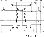
図3、図4、図5及び図6には、本発明によるコンテント・アドレッサブル・磁気ランダムアクセスメモリ(CAMRAMs)のさらにいくつかの実施形態が示される。種々の実施形態には、異なる導電型トランジスタ(例えば、N導電型及びP導電型)と異なる位置の種々の素子のような接続回路における電位変化が示される。図7には、CAMRAMセル10または他のあらゆる形態のセルの拡大図が示されるとともに、種々のI/O接続が示される。
3, 4, 5 and 6 illustrate some further embodiments of content addressable magnetic random access memories (CAMRAMs) according to the present invention. Various embodiments show potential changes in connection circuits such as different conductivity type transistors (eg, N conductivity type and P conductivity type) and various elements at different locations. FIG. 7 shows an enlarged view of the
次に図8には、各セルが図7のセル10と同様な構成のCAMRAMセルアレイ50が示される。アレイにおけるCAMRAMセルは行および列に配置され、各行にはn個のセルが、各列にはm個のセルが配置され、n及びmはあらゆる整数を表す。アレイにおける各セルはタグプログラミングビットライン及び反転タグプログラミングビットライン(それぞれBL0〜BLn、BLN0〜BLNnとして表記される)により接続され、イネーブルライン(EN0〜ENnとして表記される)は列に沿って延び、ワードライン(WL0〜WLmとして表記される)、デジットライン(DL0〜DLmとして表記される)、及びマッチライン(ML0〜MLmとして表記される)は行に沿って延びている。マッチラインML0〜MLmは一致検出回路51に接続され、検出回路51はマッチラインのいずれが一致しているかを検出し、一致信号を出力する(M0〜Miとして表記される)。
Next, FIG. 8 shows a
図1を再度参照すると、相補的情報は次のプロセスによりアレイ50のセルの各セルに書き込まれる。書き込まれている状態のセルを、ロジック0をイネーブルラインに印加する(EN=0)ことにより無効にする。無効期間中に接点24,27をVddに維持するが、この動作は書き込み動作の後、直ちに生じる読み出し及び検索モードへの移行を迅速に行うために重要となる。同時に、ロジック0を印加する(WL=0)ことによりワードラインを無効にする。プログラムビットラインPBL及びPBLNの対を選択するか、または、プログラムビットラインの全ての対を選択して書き込み速度を上げ、一つのデジットラインDLを選択する。選択した書き込みビットラインPBL,PBLN及び選択したデジットラインDLに適切な大きさの電流を流すことにより、特定の行に沿った選択セルが書き込まれる。例えば、PBL0とPBLN0を選択すると第1列のセルが選択される。DL0を選択すると第1列の第1セルが選択される。次に、ラインPBL0,PBLN0及びDL0に適切な大きさの電流を流すことにより、第1列の第1セルに所望の相補的
情報を書き込む。
Referring back to FIG. 1, complementary information is written to each cell of the
検索モードにおいては、次のプロセスが行われる。アレイ50のうち選択された列のセルを、選択されたイネーブルラインにロジック1を印加する(EN=1)ことにより有効にし、イネーブルラインを無効状態(EN=0)から引き上げる。同時に、ワードラインを無効にする(WL=0)。セルが無効になる(EN=0)と、マッチラインMLはグランドにプリチャージする必要がある。タグビットラインPBL及びPBLNは接地する。一旦、セルが無効になり、タグビットラインが接地されると、トランジスタ28,22,21とMTJ12及びトランジスタ29,26,25とMTJ14が再生+Vcをフィードバックすることにより、接点24をVddに維持し、接点27をグランドに近い電圧に引き下げ、或いは逆に、すなわち、接点27をVddに維持し、接点24をグランドに近い電圧に引き下げる。接点24,27の電圧はトランジスタ40及び38のゲートにそれぞれ現われる。このようにして、トランジスタ40,41、或いは、トランジスタ37,38のいずれかは、タグビットラインBL及びBLN経由の入力アドレスに依存する形でマッチラインMLをプルアップする。
In the search mode, the following process is performed. The cells in the selected column of the
以上のプロセスにより、アレイ50における検索開始の準備が整う。この結果、イネーブルラインはハイ(high)となり、高速の並列検索を開始することができる。入力ワード(BL0・・・BLN)はアレイ50のある行に保存されるデータと比較される。各CAMRAMセル10に保存されるデータは「タグ」として知られ、タグワードは一行のCAMRAMセル10により形成される。各行のCAMRAMセル10、または各タグワードはマッチライン(ML0・・・MLN)に接続される。タグワードのビットのいずれかに不一致があると、該当するマッチラインがプルダウンされる。あるタグワードの全ビットが入力ワードと一致すると、該当するマッチラインはハイのままとなる。一致検出回路51はマッチラインの変化を検出し、レジスタにその結果を保存する。アレイ50中の一つまたはそれ以上のビットのマスキング、すなわち、「マスクされた問合せビットポジション( masked interrogate bit position)」(と以後呼ぶこととする)は、所望のビットのイネーブルラインをローに下げることにより容易に実現できる。イネーブルラインがローとなっているビットは、該当する列に沿ったCAMRAMセルをターンオフさせ、局所マスキングすることとなって電力を節約できる。
With the above process, the search for the
読み出し動作モードにおいては、CAMRAMはランダムアクセスメモリとして使用できるか、または、それに連続的にアクセスできるように設計することができる。読み出し動作は次のように行われる。イネーブルラインを無効にする(EN=0)と、タグビットラインBL及びBLNをVddにプリチャージする。接点24,27、並びにビットラインBL及びBLNはVddとなる。プログラミングビットラインPBL及びPBLNは接地する。一致検出回路51を無効にすると、読み出し動作中においてはタグビットラインBL及びBLNはロジックハイレベルまたはロジックローレベルのいずれかであり、この状態によりトランジスタ37,41がターンオンまたはターンオフするので、マッチラインMLが変化することとなる。ランダムアクセス期間中に一致検出回路51を無効にすると、一致検出回路51を不必要に変化させることを防止することができる。ワードラインWLを有効(WL=1)にし、選択されたセルを有効(EN=1)にする。MTJ12,14の状態に依存する形で、接点24,27はVddとなる、またはグランドよりも少し高い電圧となる。接点24または接点27がVddであると、タグビットラインBLまたはBLNはそれぞれVddを維持する。しかしながら、接点24または接点27がグランドよりも少し高い電圧であると、タグビットラインBLまたはBLNはそれぞれグランドに向かってプルダウンされ、そのとき、高速センスアンプ(図示せず)はタグビットラインBL及びBLNに現れる電圧を差分として高速に検知し、検知したデータを出力する。ここで、走査メカニズムは電圧モードまたは電流モードのいずれかにあることを理解されたい。
In the read mode of operation, the CAMRAM can be used as a random access memory or can be designed to allow continuous access to it. The read operation is performed as follows. When the enable line is disabled (EN = 0), the tag bit lines BL and BLN are precharged to Vdd. The
好適には、トランジスタ21,22及び28とトランジスタ25,26及び29、それにMTJ12,14の抵抗は、MTJ12,14の両端に印加される電圧が約100mV〜400mVの範囲となるように選択される。この範囲内で最大MR(最大抵抗と最小抵抗の比)が得られる。一般的に、MTJ12,14の両端に印加される電圧が低くなれば、MRが高くなり、消費電流が小さくなる。
Preferably, the resistances of
単一MTJセルは、処理、バイアス電圧変動、温度等に起因する抵抗変動に遭遇するので、これらの変動の要因と考えられるものが速度劣化につながる。しかしながら、差動形式で書き込まれるデュアルMTJセルにおいては、ここに記載するCAMRAMセルにおけるように、このような変動はすべて同相モードであり、自動的に消去される。さらに、利用可能な出力信号はデュアルMTJ及び差動動作により2倍化される。また、単一MTJセルが、メモリアレイの端部においてデータセンス及びデータ処理を行うメインメモリに使用される場合(例えば、本願とともに係属中であり、2000年8月28日出願された米国出願番号第09/649114号であり、同じ譲受人に譲渡された「高密度MRAMセルアレイ(HIGH DENSITY MRAM CELL ARRAY)」と題する出願を参照されたい)、CAMRAMはメインメモリよりもかなり高速である。 Since a single MTJ cell encounters resistance fluctuations due to processing, bias voltage fluctuations, temperature, etc., what is considered a source of these fluctuations leads to speed degradation. However, in dual MTJ cells written in a differential format, all such variations are in the common mode and are automatically erased, as in the CAMRAM cell described herein. Furthermore, the available output signal is doubled by dual MTJ and differential operation. Also, if a single MTJ cell is used for the main memory that performs data sensing and data processing at the end of the memory array (eg, US application number filed Aug. 28, 2000, pending with this application). No. 09/649114, see the application entitled “High Density MRAM Cell Array” assigned to the same assignee), CAMRAM is much faster than main memory.
ここで、SRAMをベースとするCAMセルはセルの位置でターンオフさせることができず、マスキングはアレイの周辺で行わなければならないので、このCAMセルはマスクすることができないのに対し、CAMRAMセルは、情報を失うことなくセルの位置において局所的にマスキングすることが可能であることにも留意されたい。CAMRAMセルを局所的にマスキングすると電力を相当節約できることとなる。CAMRAMセルはセルのイネーブルラインEN入力を通してマスクすることができ、この入力は一列のセルを接続するイネーブルラインENに接続される。また、CAMRAMセルは、高密度MRAM(上記に引用された本願とともに係属中の出願を参照されたし)に用いられる標準のMTJ構造と異なる構造にする必要は全く無い。 Here, an SRAM-based CAM cell cannot be turned off at the cell location and masking must be done at the periphery of the array, so this CAM cell cannot be masked, whereas a CAMRAM cell Note also that it is possible to mask locally at the cell location without losing information. Masking the CAMRAM cell locally can save considerable power. The CAMRAM cell can be masked through the cell's enable line EN input, which is connected to the enable line EN that connects a row of cells. Also, the CAMRAM cell need not have a different structure from the standard MTJ structure used for high density MRAM (see the pending application with the above cited application).
以上のように、新規の改良されたコンテント・アドレッサブル・磁気ランダムアクセスメモリセルを開示するが、このセルは少なくともSRAMをベースとするメモリと同程度に高速であり、不揮発性である。また、ビットライン電圧は検索中に一致または不一致が検出される場合でも比較的一定に維持される。各セルは差動動作するので、処理に起因する抵抗変動、バイアス電圧変動、温度等は自動的に除去され、動作のために速度を犠牲にする必要が無い。さらに、差動で動作するのでより大きな信号を供給して一層効果的な検出及び動作が可能となる。 Thus, a new and improved content-addressable-magnetic random access memory cell is disclosed, which is at least as fast as a SRAM-based memory and is non-volatile. Also, the bit line voltage is kept relatively constant even if a match or mismatch is detected during the search. Since each cell operates differentially, resistance variation, bias voltage variation, temperature, and the like due to processing are automatically removed, and there is no need to sacrifice speed for operation. Furthermore, since it operates differentially, a larger signal can be supplied to enable more effective detection and operation.
CAMRAMセルは不揮発性であるので、新規のキャッシュ設計態様が生成され、その結果、新規のCPUアーキテクチャが生まれる。高速の検索エンジンは新規のCAMRAMセルを使用して設計することが可能であり、このように設計することにより、関連データを処理するための数多くのシステム及びアプリケーションが提供される。 Since CAMRAM cells are non-volatile, a new cache design aspect is created, resulting in a new CPU architecture. A fast search engine can be designed using the new CAMRAM cell, which provides a number of systems and applications for processing relevant data.
この技術分野の当業者には、一般的にビットラインはMTJセルアレイの各列に関連付けられ、デジットラインはアレイの各行に関連付けられることが理解できるであろう。ビットライン及びデジットラインはアレイの個々のセルを指定するために使用され、それによりアレイにおける情報の読み出し及び書き込み又は保存の双方を行なう。この技術分野の当業者には明らかなことであるが、列及び行は容易に入れ替えることが可能であり、本開示においてはこのような用語は置き換え可能である。また、種々のライン、例えば、ビットライン、ワードライン、デジットライン、セレクトライン等の特殊な呼び名は包括的な名称を意図したものであり、説明を簡単にするためにのみ使用されるのであって、決して本発明を制限するためのものではない。 One skilled in the art will appreciate that a bit line is typically associated with each column of the MTJ cell array and a digit line is associated with each row of the array. Bit lines and digit lines are used to designate individual cells of the array, thereby both reading and writing or storing information in the array. As will be apparent to those skilled in the art, the columns and rows can be easily interchanged, and such terms are interchangeable in this disclosure. Also, special names such as various lines, eg bit line, word line, digit line, select line, etc. are intended to be comprehensive names and are used only for ease of explanation. It is not intended to limit the invention in any way.
本発明の特定の実施形態を示し、記載してきたが、この技術分野の当業者はこれらの実施形態にさらに変形及び改良を加えることができる。従って、本発明が示された特殊な形態に限定されず、添付の請求項は、本発明の技術思想及び技術範囲を逸脱しない範囲のあらゆる変形を含むことが理解されよう。 While particular embodiments of the present invention have been shown and described, those skilled in the art can make further modifications and improvements to these embodiments. Accordingly, it is to be understood that the invention is not limited to the specific forms shown, and that the appended claims encompass all modifications that do not depart from the spirit and scope of the invention.
Claims (2)
前記第1接点は第1トランジスタを通してビットラインに接続され、第1トランジスタの制御端子はワードラインに接続され、前記第2接点は第2トランジスタを通して反転ビットラインに接続され、第2トランジスタの制御端子は前記ワードラインに接続されることと、The first contact is connected to the bit line through the first transistor, the control terminal of the first transistor is connected to the word line, the second contact is connected to the inverted bit line through the second transistor, and the control terminal of the second transistor Is connected to the word line;
前記第1接点は第1イネーブルトランジスタを通して電源入力端子に接続され、第1イネーブルトランジスタの制御端子は前記イネーブルラインに接続され、前記第2接点は第2イネーブルトランジスタを通して前記電源入力端子に接続され、第2イネーブルトランジスタの制御端子が前記イネーブルラインに接続されることと、The first contact is connected to a power input terminal through a first enable transistor, a control terminal of the first enable transistor is connected to the enable line, and the second contact is connected to the power input terminal through a second enable transistor; A control terminal of the second enable transistor is connected to the enable line;
前記第1接点は第1差動トランジスタを通して前記電源入力端子に接続され、第1差動トランジスタの制御端子は前記第1の直列接続された対をなすトランジスタの内の第2のトランジスタの制御端子と前記第2接点とに接続され、前記第2接点は第2差動トランジスタを通して前記電源入力端子に接続され、第2差動トランジスタの制御端子は前記第2の直列接続された対をなすトランジスタの内の第2のトランジスタの制御端子と前記第1接点に接続されることと、The first contact is connected to the power input terminal through a first differential transistor, and a control terminal of the first differential transistor is a control terminal of a second transistor of the first pair of transistors connected in series. And the second contact, the second contact is connected to the power input terminal through a second differential transistor, and the control terminal of the second differential transistor is the second series-connected transistor. Connected to the control terminal of the second transistor of the first and the first contact;
前記電源入力端子とマッチラインとの間に接続される第1の直列接続された対をなすマッチトランジスタと、その第1の直列接続された対をなすマッチトランジスタのうちの第1のマッチトランジスタの制御端子が前記ビットラインに接続され、前記第1の直列接続された対をなすマッチトランジスタのうちの第2のマッチトランジスタの制御端子が前記第2接点に接続されることと、前記電源入力端子と前記マッチラインとの間に接続される第2の直列接続された対をなすマッチトランジスタと、その第2の直列接続された対をなすマッチトランジスタうちの第1のマッチトランジスタの制御端子が前記反転ビットライA first series-connected match transistor connected between the power input terminal and the match line, and a first match transistor of the first series-connected match transistors. A control terminal connected to the bit line, a control terminal of a second match transistor of the first series connected match transistors connected to the second contact, and the power input terminal And a match terminal forming a second series-connected pair connected between the match line and the control terminal of the first match transistor of the second series-connected match transistors Reverse bit line
ンに接続され、前記第2の直列接続された対をなすマッチトランジスタうちの第2のマッチトランジスタの制御端子が前記第1接点に接続されることとを含む、コンテント・アドレッサブル・磁気ランダムアクセスメモリセル。And a control terminal of a second match transistor of the second series-connected match transistors is connected to the first contact, a content addressable magnetic random access memory cell.
前記ラッチに接続されているイネーブルラインと、An enable line connected to the latch;
マッチラインと前記ラッチとの間に結合され、第1および第2ビットラインに応答して、マッチラインを変化させる回路とを備える、磁気ランダムアクセスメモリセル。A magnetic random access memory cell, comprising: a circuit coupled between a match line and the latch, the circuit changing the match line in response to the first and second bit lines.
Applications Claiming Priority (2)
| Application Number | Priority Date | Filing Date | Title |
|---|---|---|---|
| US09/774,934 US6304477B1 (en) | 2001-01-31 | 2001-01-31 | Content addressable magnetic random access memory |
| PCT/US2002/000786 WO2002061755A1 (en) | 2001-01-31 | 2002-01-11 | Content addressable magnetic random access memory |
Publications (3)
| Publication Number | Publication Date |
|---|---|
| JP2004525473A JP2004525473A (en) | 2004-08-19 |
| JP2004525473A5 JP2004525473A5 (en) | 2005-12-22 |
| JP3793507B2 true JP3793507B2 (en) | 2006-07-05 |
Family
ID=25102747
Family Applications (1)
| Application Number | Title | Priority Date | Filing Date |
|---|---|---|---|
| JP2002561835A Expired - Fee Related JP3793507B2 (en) | 2001-01-31 | 2002-01-11 | Content, addressable, magnetic random access memory |
Country Status (6)
| Country | Link |
|---|---|
| US (1) | US6304477B1 (en) |
| JP (1) | JP3793507B2 (en) |
| KR (1) | KR100869659B1 (en) |
| CN (1) | CN1524271B (en) |
| TW (1) | TW565844B (en) |
| WO (1) | WO2002061755A1 (en) |
Families Citing this family (179)
| Publication number | Priority date | Publication date | Assignee | Title |
|---|---|---|---|---|
| US6515895B2 (en) * | 2001-01-31 | 2003-02-04 | Motorola, Inc. | Non-volatile magnetic register |
| US6512690B1 (en) * | 2001-08-15 | 2003-01-28 | Read-Rite Corporation | High sensitivity common source amplifier MRAM cell, memory array and read/write scheme |
| KR100406924B1 (en) * | 2001-10-12 | 2003-11-21 | 삼성전자주식회사 | Content addressable memory cell |
| SG102019A1 (en) * | 2001-12-04 | 2004-02-27 | Inst Data Storage | Magnetic tunnel junction magnetic random access memory |
| JP4278325B2 (en) | 2001-12-19 | 2009-06-10 | 株式会社ルネサステクノロジ | Semiconductor integrated circuit device |
| US7237100B2 (en) * | 2002-01-09 | 2007-06-26 | International Business Machines Corporation | Transaction redirection mechanism for handling late specification changes and design errors |
| US6548849B1 (en) | 2002-01-31 | 2003-04-15 | Sharp Laboratories Of America, Inc. | Magnetic yoke structures in MRAM devices to reduce programming power consumption and a method to make the same |
| JP4133149B2 (en) * | 2002-09-12 | 2008-08-13 | 株式会社ルネサステクノロジ | Semiconductor memory device |
| JP4294307B2 (en) * | 2002-12-26 | 2009-07-08 | 株式会社ルネサステクノロジ | Nonvolatile storage device |
| KR100479810B1 (en) * | 2002-12-30 | 2005-03-31 | 주식회사 하이닉스반도체 | Non-volatile memory device |
| US7173846B2 (en) * | 2003-02-13 | 2007-02-06 | Taiwan Semiconductor Manufacturing Company, Ltd. | Magnetic RAM and array architecture using a two transistor, one MTJ cell |
| EP2261928B1 (en) * | 2003-10-22 | 2012-09-05 | STMicroelectronics Srl | A content addressable memory cell |
| US7333360B2 (en) * | 2003-12-23 | 2008-02-19 | Freescale Semiconductor, Inc. | Apparatus for pulse testing a MRAM device and method therefore |
| US7339818B2 (en) * | 2004-06-04 | 2008-03-04 | Micron Technology, Inc. | Spintronic devices with integrated transistors |
| US7196921B2 (en) * | 2004-07-19 | 2007-03-27 | Silicon Storage Technology, Inc. | High-speed and low-power differential non-volatile content addressable memory cell and array |
| US7130206B2 (en) * | 2004-09-30 | 2006-10-31 | Infineon Technologies Ag | Content addressable memory cell including resistive memory elements |
| US7675765B2 (en) * | 2005-11-03 | 2010-03-09 | Agate Logic, Inc. | Phase-change memory (PCM) based universal content-addressable memory (CAM) configured as binary/ternary CAM |
| JP4231887B2 (en) * | 2006-09-28 | 2009-03-04 | 株式会社東芝 | Nonvolatile latch circuit and nonvolatile flip-flop circuit |
| TWI449040B (en) * | 2006-10-06 | 2014-08-11 | Crocus Technology Sa | System and method for providing content-addressable magnetoresistive random access memory cells |
| JP4435189B2 (en) * | 2007-02-15 | 2010-03-17 | 株式会社東芝 | Magnetic storage element and magnetic storage device |
| US8243502B2 (en) * | 2007-12-14 | 2012-08-14 | Nec Corporation | Nonvolatile latch circuit and logic circuit using the same |
| ATE538474T1 (en) * | 2008-04-07 | 2012-01-15 | Crocus Technology Sa | SYSTEM AND METHOD FOR WRITING DATA TO MAGNETORRESISTIVE RANDOM ACCESS MEMORY CELLS |
| EP2124228B1 (en) * | 2008-05-20 | 2014-03-05 | Crocus Technology | Magnetic random access memory with an elliptical junction |
| US8031519B2 (en) * | 2008-06-18 | 2011-10-04 | Crocus Technology S.A. | Shared line magnetic random access memory cells |
| US8650355B2 (en) * | 2008-10-15 | 2014-02-11 | Seagate Technology Llc | Non-volatile resistive sense memory on-chip cache |
| US8228703B2 (en) * | 2008-11-04 | 2012-07-24 | Crocus Technology Sa | Ternary Content Addressable Magnetoresistive random access memory cell |
| JP2010192053A (en) * | 2009-02-19 | 2010-09-02 | Toshiba Corp | Semiconductor memory device |
| US8489801B2 (en) * | 2009-03-04 | 2013-07-16 | Henry F. Huang | Non-volatile memory with hybrid index tag array |
| US8023299B1 (en) * | 2009-04-09 | 2011-09-20 | Netlogic Microsystems, Inc. | Content addressable memory device having spin torque transfer memory cells |
| JP5483265B2 (en) * | 2009-05-29 | 2014-05-07 | 日本電気株式会社 | Non-volatile CAM |
| CN101567214B (en) * | 2009-06-10 | 2011-06-15 | 哈尔滨工业大学 | Line selector applicable to reading and wiring functions of nine-transistor memory unit |
| US8120939B2 (en) * | 2009-09-24 | 2012-02-21 | Taiwan Semiconductor Manufacturing Co., Ltd. | ROM cell having an isolation transistor formed between first and second pass transistors and connected between a differential bitline pair |
| JP2012089205A (en) * | 2010-10-20 | 2012-05-10 | Renesas Electronics Corp | Associative storage device |
| US8729545B2 (en) | 2011-04-28 | 2014-05-20 | Semiconductor Energy Laboratory Co., Ltd. | Semiconductor memory device |
| JP6013773B2 (en) | 2011-05-13 | 2016-10-25 | 株式会社半導体エネルギー研究所 | Semiconductor device |
| US8908407B1 (en) * | 2011-07-30 | 2014-12-09 | Rambus Inc. | Content addressable memory (“CAM”) |
| US8638582B1 (en) | 2011-08-23 | 2014-01-28 | Netlogic Microsystems, Inc. | Content addressable memory with base-three numeral system |
| JP6004465B2 (en) * | 2012-03-26 | 2016-10-05 | 国立大学法人東北大学 | Nonvolatile functional memory device |
| JP6179818B2 (en) * | 2012-09-06 | 2017-08-16 | 日本電気株式会社 | Non-volatile associative memory |
| US9158667B2 (en) | 2013-03-04 | 2015-10-13 | Micron Technology, Inc. | Apparatuses and methods for performing logical operations using sensing circuitry |
| US8964496B2 (en) | 2013-07-26 | 2015-02-24 | Micron Technology, Inc. | Apparatuses and methods for performing compare operations using sensing circuitry |
| US8971124B1 (en) | 2013-08-08 | 2015-03-03 | Micron Technology, Inc. | Apparatuses and methods for performing logical operations using sensing circuitry |
| US9153305B2 (en) | 2013-08-30 | 2015-10-06 | Micron Technology, Inc. | Independently addressable memory array address spaces |
| US9019785B2 (en) | 2013-09-19 | 2015-04-28 | Micron Technology, Inc. | Data shifting via a number of isolation devices |
| US9449675B2 (en) * | 2013-10-31 | 2016-09-20 | Micron Technology, Inc. | Apparatuses and methods for identifying an extremum value stored in an array of memory cells |
| US9430191B2 (en) | 2013-11-08 | 2016-08-30 | Micron Technology, Inc. | Division operations for memory |
| US9934856B2 (en) | 2014-03-31 | 2018-04-03 | Micron Technology, Inc. | Apparatuses and methods for comparing data patterns in memory |
| US9779019B2 (en) | 2014-06-05 | 2017-10-03 | Micron Technology, Inc. | Data storage layout |
| US9786335B2 (en) | 2014-06-05 | 2017-10-10 | Micron Technology, Inc. | Apparatuses and methods for performing logical operations using sensing circuitry |
| US9830999B2 (en) | 2014-06-05 | 2017-11-28 | Micron Technology, Inc. | Comparison operations in memory |
| US9496023B2 (en) | 2014-06-05 | 2016-11-15 | Micron Technology, Inc. | Comparison operations on logical representations of values in memory |
| US9711207B2 (en) | 2014-06-05 | 2017-07-18 | Micron Technology, Inc. | Performing logical operations using sensing circuitry |
| US10074407B2 (en) | 2014-06-05 | 2018-09-11 | Micron Technology, Inc. | Apparatuses and methods for performing invert operations using sensing circuitry |
| US9711206B2 (en) | 2014-06-05 | 2017-07-18 | Micron Technology, Inc. | Performing logical operations using sensing circuitry |
| US9455020B2 (en) | 2014-06-05 | 2016-09-27 | Micron Technology, Inc. | Apparatuses and methods for performing an exclusive or operation using sensing circuitry |
| US9449674B2 (en) | 2014-06-05 | 2016-09-20 | Micron Technology, Inc. | Performing logical operations using sensing circuitry |
| US9910787B2 (en) | 2014-06-05 | 2018-03-06 | Micron Technology, Inc. | Virtual address table |
| US9704540B2 (en) | 2014-06-05 | 2017-07-11 | Micron Technology, Inc. | Apparatuses and methods for parity determination using sensing circuitry |
| US9747961B2 (en) | 2014-09-03 | 2017-08-29 | Micron Technology, Inc. | Division operations in memory |
| US10068652B2 (en) | 2014-09-03 | 2018-09-04 | Micron Technology, Inc. | Apparatuses and methods for determining population count |
| US9589602B2 (en) | 2014-09-03 | 2017-03-07 | Micron Technology, Inc. | Comparison operations in memory |
| US9740607B2 (en) | 2014-09-03 | 2017-08-22 | Micron Technology, Inc. | Swap operations in memory |
| US9904515B2 (en) | 2014-09-03 | 2018-02-27 | Micron Technology, Inc. | Multiplication operations in memory |
| US9898252B2 (en) | 2014-09-03 | 2018-02-20 | Micron Technology, Inc. | Multiplication operations in memory |
| US9847110B2 (en) | 2014-09-03 | 2017-12-19 | Micron Technology, Inc. | Apparatuses and methods for storing a data value in multiple columns of an array corresponding to digits of a vector |
| US9940026B2 (en) | 2014-10-03 | 2018-04-10 | Micron Technology, Inc. | Multidimensional contiguous memory allocation |
| US9836218B2 (en) | 2014-10-03 | 2017-12-05 | Micron Technology, Inc. | Computing reduction and prefix sum operations in memory |
| US10163467B2 (en) | 2014-10-16 | 2018-12-25 | Micron Technology, Inc. | Multiple endianness compatibility |
| US10147480B2 (en) | 2014-10-24 | 2018-12-04 | Micron Technology, Inc. | Sort operation in memory |
| US9779784B2 (en) | 2014-10-29 | 2017-10-03 | Micron Technology, Inc. | Apparatuses and methods for performing logical operations using sensing circuitry |
| TWI550632B (en) * | 2014-10-30 | 2016-09-21 | 華邦電子股份有限公司 | Non-volatile static random access memory circuits |
| US9747960B2 (en) | 2014-12-01 | 2017-08-29 | Micron Technology, Inc. | Apparatuses and methods for converting a mask to an index |
| US10073635B2 (en) | 2014-12-01 | 2018-09-11 | Micron Technology, Inc. | Multiple endianness compatibility |
| US10032493B2 (en) | 2015-01-07 | 2018-07-24 | Micron Technology, Inc. | Longest element length determination in memory |
| US10061590B2 (en) | 2015-01-07 | 2018-08-28 | Micron Technology, Inc. | Generating and executing a control flow |
| US9583163B2 (en) | 2015-02-03 | 2017-02-28 | Micron Technology, Inc. | Loop structure for operations in memory |
| WO2016126472A1 (en) | 2015-02-06 | 2016-08-11 | Micron Technology, Inc. | Apparatuses and methods for scatter and gather |
| EP3254286B1 (en) | 2015-02-06 | 2019-09-11 | Micron Technology, INC. | Apparatuses and methods for parallel writing to multiple memory device locations |
| EP3254287A4 (en) | 2015-02-06 | 2018-08-08 | Micron Technology, INC. | Apparatuses and methods for memory device as a store for program instructions |
| US10522212B2 (en) | 2015-03-10 | 2019-12-31 | Micron Technology, Inc. | Apparatuses and methods for shift decisions |
| US9741399B2 (en) | 2015-03-11 | 2017-08-22 | Micron Technology, Inc. | Data shift by elements of a vector in memory |
| US9898253B2 (en) | 2015-03-11 | 2018-02-20 | Micron Technology, Inc. | Division operations on variable length elements in memory |
| EP3268965A4 (en) | 2015-03-12 | 2018-10-03 | Micron Technology, INC. | Apparatuses and methods for data movement |
| US10146537B2 (en) | 2015-03-13 | 2018-12-04 | Micron Technology, Inc. | Vector population count determination in memory |
| TWI579860B (en) * | 2015-03-23 | 2017-04-21 | 國立成功大學 | A memory cell and a content addressable memory with the memory cell |
| US10049054B2 (en) | 2015-04-01 | 2018-08-14 | Micron Technology, Inc. | Virtual register file |
| US10140104B2 (en) | 2015-04-14 | 2018-11-27 | Micron Technology, Inc. | Target architecture determination |
| US9959923B2 (en) | 2015-04-16 | 2018-05-01 | Micron Technology, Inc. | Apparatuses and methods to reverse data stored in memory |
| US10073786B2 (en) | 2015-05-28 | 2018-09-11 | Micron Technology, Inc. | Apparatuses and methods for compute enabled cache |
| US9704541B2 (en) | 2015-06-12 | 2017-07-11 | Micron Technology, Inc. | Simulating access lines |
| US9921777B2 (en) | 2015-06-22 | 2018-03-20 | Micron Technology, Inc. | Apparatuses and methods for data transfer from sensing circuitry to a controller |
| US9996479B2 (en) | 2015-08-17 | 2018-06-12 | Micron Technology, Inc. | Encryption of executables in computational memory |
| US9905276B2 (en) | 2015-12-21 | 2018-02-27 | Micron Technology, Inc. | Control of sensing components in association with performing operations |
| US9952925B2 (en) | 2016-01-06 | 2018-04-24 | Micron Technology, Inc. | Error code calculation on sensing circuitry |
| US10048888B2 (en) | 2016-02-10 | 2018-08-14 | Micron Technology, Inc. | Apparatuses and methods for partitioned parallel data movement |
| US9892767B2 (en) | 2016-02-12 | 2018-02-13 | Micron Technology, Inc. | Data gathering in memory |
| US9971541B2 (en) | 2016-02-17 | 2018-05-15 | Micron Technology, Inc. | Apparatuses and methods for data movement |
| US10956439B2 (en) | 2016-02-19 | 2021-03-23 | Micron Technology, Inc. | Data transfer with a bit vector operation device |
| US9899070B2 (en) | 2016-02-19 | 2018-02-20 | Micron Technology, Inc. | Modified decode for corner turn |
| US9697876B1 (en) | 2016-03-01 | 2017-07-04 | Micron Technology, Inc. | Vertical bit vector shift in memory |
| US10262721B2 (en) | 2016-03-10 | 2019-04-16 | Micron Technology, Inc. | Apparatuses and methods for cache invalidate |
| US9997232B2 (en) | 2016-03-10 | 2018-06-12 | Micron Technology, Inc. | Processing in memory (PIM) capable memory device having sensing circuitry performing logic operations |
| US10379772B2 (en) | 2016-03-16 | 2019-08-13 | Micron Technology, Inc. | Apparatuses and methods for operations using compressed and decompressed data |
| US9910637B2 (en) | 2016-03-17 | 2018-03-06 | Micron Technology, Inc. | Signed division in memory |
| US10120740B2 (en) | 2016-03-22 | 2018-11-06 | Micron Technology, Inc. | Apparatus and methods for debugging on a memory device |
| US10388393B2 (en) | 2016-03-22 | 2019-08-20 | Micron Technology, Inc. | Apparatus and methods for debugging on a host and memory device |
| US11074988B2 (en) | 2016-03-22 | 2021-07-27 | Micron Technology, Inc. | Apparatus and methods for debugging on a host and memory device |
| US10474581B2 (en) | 2016-03-25 | 2019-11-12 | Micron Technology, Inc. | Apparatuses and methods for cache operations |
| US10977033B2 (en) | 2016-03-25 | 2021-04-13 | Micron Technology, Inc. | Mask patterns generated in memory from seed vectors |
| US10430244B2 (en) | 2016-03-28 | 2019-10-01 | Micron Technology, Inc. | Apparatuses and methods to determine timing of operations |
| US10074416B2 (en) | 2016-03-28 | 2018-09-11 | Micron Technology, Inc. | Apparatuses and methods for data movement |
| US10453502B2 (en) | 2016-04-04 | 2019-10-22 | Micron Technology, Inc. | Memory bank power coordination including concurrently performing a memory operation in a selected number of memory regions |
| US10607665B2 (en) | 2016-04-07 | 2020-03-31 | Micron Technology, Inc. | Span mask generation |
| US9818459B2 (en) | 2016-04-19 | 2017-11-14 | Micron Technology, Inc. | Invert operations using sensing circuitry |
| US9659605B1 (en) | 2016-04-20 | 2017-05-23 | Micron Technology, Inc. | Apparatuses and methods for performing corner turn operations using sensing circuitry |
| US10153008B2 (en) | 2016-04-20 | 2018-12-11 | Micron Technology, Inc. | Apparatuses and methods for performing corner turn operations using sensing circuitry |
| US10042608B2 (en) | 2016-05-11 | 2018-08-07 | Micron Technology, Inc. | Signed division in memory |
| US9659610B1 (en) | 2016-05-18 | 2017-05-23 | Micron Technology, Inc. | Apparatuses and methods for shifting data |
| US10049707B2 (en) | 2016-06-03 | 2018-08-14 | Micron Technology, Inc. | Shifting data |
| US10387046B2 (en) | 2016-06-22 | 2019-08-20 | Micron Technology, Inc. | Bank to bank data transfer |
| US10037785B2 (en) | 2016-07-08 | 2018-07-31 | Micron Technology, Inc. | Scan chain operation in sensing circuitry |
| US10388360B2 (en) | 2016-07-19 | 2019-08-20 | Micron Technology, Inc. | Utilization of data stored in an edge section of an array |
| US10733089B2 (en) | 2016-07-20 | 2020-08-04 | Micron Technology, Inc. | Apparatuses and methods for write address tracking |
| US10387299B2 (en) | 2016-07-20 | 2019-08-20 | Micron Technology, Inc. | Apparatuses and methods for transferring data |
| US9972367B2 (en) | 2016-07-21 | 2018-05-15 | Micron Technology, Inc. | Shifting data in sensing circuitry |
| US9767864B1 (en) | 2016-07-21 | 2017-09-19 | Micron Technology, Inc. | Apparatuses and methods for storing a data value in a sensing circuitry element |
| US10303632B2 (en) | 2016-07-26 | 2019-05-28 | Micron Technology, Inc. | Accessing status information |
| US10468087B2 (en) | 2016-07-28 | 2019-11-05 | Micron Technology, Inc. | Apparatuses and methods for operations in a self-refresh state |
| US9990181B2 (en) | 2016-08-03 | 2018-06-05 | Micron Technology, Inc. | Apparatuses and methods for random number generation |
| US9934857B2 (en) * | 2016-08-04 | 2018-04-03 | Hewlett Packard Enterprise Development Lp | Ternary content addressable memories having a bit cell with memristors and serially connected match-line transistors |
| US11029951B2 (en) | 2016-08-15 | 2021-06-08 | Micron Technology, Inc. | Smallest or largest value element determination |
| US10606587B2 (en) | 2016-08-24 | 2020-03-31 | Micron Technology, Inc. | Apparatus and methods related to microcode instructions indicating instruction types |
| US10466928B2 (en) | 2016-09-15 | 2019-11-05 | Micron Technology, Inc. | Updating a register in memory |
| US10387058B2 (en) | 2016-09-29 | 2019-08-20 | Micron Technology, Inc. | Apparatuses and methods to change data category values |
| US10014034B2 (en) | 2016-10-06 | 2018-07-03 | Micron Technology, Inc. | Shifting data in sensing circuitry |
| US10529409B2 (en) | 2016-10-13 | 2020-01-07 | Micron Technology, Inc. | Apparatuses and methods to perform logical operations using sensing circuitry |
| US9805772B1 (en) | 2016-10-20 | 2017-10-31 | Micron Technology, Inc. | Apparatuses and methods to selectively perform logical operations |
| CN207637499U (en) | 2016-11-08 | 2018-07-20 | 美光科技公司 | The equipment for being used to form the computation module above memory cell array |
| US10423353B2 (en) | 2016-11-11 | 2019-09-24 | Micron Technology, Inc. | Apparatuses and methods for memory alignment |
| US9761300B1 (en) | 2016-11-22 | 2017-09-12 | Micron Technology, Inc. | Data shift apparatuses and methods |
| US10402340B2 (en) | 2017-02-21 | 2019-09-03 | Micron Technology, Inc. | Memory array page table walk |
| US10268389B2 (en) | 2017-02-22 | 2019-04-23 | Micron Technology, Inc. | Apparatuses and methods for in-memory operations |
| US10403352B2 (en) | 2017-02-22 | 2019-09-03 | Micron Technology, Inc. | Apparatuses and methods for compute in data path |
| US10838899B2 (en) | 2017-03-21 | 2020-11-17 | Micron Technology, Inc. | Apparatuses and methods for in-memory data switching networks |
| US11222260B2 (en) | 2017-03-22 | 2022-01-11 | Micron Technology, Inc. | Apparatuses and methods for operating neural networks |
| US10185674B2 (en) | 2017-03-22 | 2019-01-22 | Micron Technology, Inc. | Apparatus and methods for in data path compute operations |
| US10049721B1 (en) | 2017-03-27 | 2018-08-14 | Micron Technology, Inc. | Apparatuses and methods for in-memory operations |
| US10147467B2 (en) | 2017-04-17 | 2018-12-04 | Micron Technology, Inc. | Element value comparison in memory |
| US10043570B1 (en) | 2017-04-17 | 2018-08-07 | Micron Technology, Inc. | Signed element compare in memory |
| US9997212B1 (en) | 2017-04-24 | 2018-06-12 | Micron Technology, Inc. | Accessing data in memory |
| US10942843B2 (en) | 2017-04-25 | 2021-03-09 | Micron Technology, Inc. | Storing data elements of different lengths in respective adjacent rows or columns according to memory shapes |
| US10236038B2 (en) | 2017-05-15 | 2019-03-19 | Micron Technology, Inc. | Bank to bank data transfer |
| US10068664B1 (en) | 2017-05-19 | 2018-09-04 | Micron Technology, Inc. | Column repair in memory |
| US10013197B1 (en) | 2017-06-01 | 2018-07-03 | Micron Technology, Inc. | Shift skip |
| US10262701B2 (en) | 2017-06-07 | 2019-04-16 | Micron Technology, Inc. | Data transfer between subarrays in memory |
| US10152271B1 (en) | 2017-06-07 | 2018-12-11 | Micron Technology, Inc. | Data replication |
| US10318168B2 (en) | 2017-06-19 | 2019-06-11 | Micron Technology, Inc. | Apparatuses and methods for simultaneous in data path compute operations |
| US10162005B1 (en) | 2017-08-09 | 2018-12-25 | Micron Technology, Inc. | Scan chain operations |
| US10534553B2 (en) | 2017-08-30 | 2020-01-14 | Micron Technology, Inc. | Memory array accessibility |
| US10346092B2 (en) | 2017-08-31 | 2019-07-09 | Micron Technology, Inc. | Apparatuses and methods for in-memory operations using timing circuitry |
| US10416927B2 (en) | 2017-08-31 | 2019-09-17 | Micron Technology, Inc. | Processing in memory |
| US10741239B2 (en) | 2017-08-31 | 2020-08-11 | Micron Technology, Inc. | Processing in memory device including a row address strobe manager |
| US10409739B2 (en) | 2017-10-24 | 2019-09-10 | Micron Technology, Inc. | Command selection policy |
| US10522210B2 (en) | 2017-12-14 | 2019-12-31 | Micron Technology, Inc. | Apparatuses and methods for subarray addressing |
| US10332586B1 (en) | 2017-12-19 | 2019-06-25 | Micron Technology, Inc. | Apparatuses and methods for subrow addressing |
| US10614875B2 (en) | 2018-01-30 | 2020-04-07 | Micron Technology, Inc. | Logical operations using memory cells |
| US10437557B2 (en) | 2018-01-31 | 2019-10-08 | Micron Technology, Inc. | Determination of a match between data values stored by several arrays |
| US11194477B2 (en) | 2018-01-31 | 2021-12-07 | Micron Technology, Inc. | Determination of a match between data values stored by three or more arrays |
| US10725696B2 (en) | 2018-04-12 | 2020-07-28 | Micron Technology, Inc. | Command selection policy with read priority |
| US10440341B1 (en) | 2018-06-07 | 2019-10-08 | Micron Technology, Inc. | Image processor formed in an array of memory cells |
| US10769071B2 (en) | 2018-10-10 | 2020-09-08 | Micron Technology, Inc. | Coherent memory access |
| US11175915B2 (en) | 2018-10-10 | 2021-11-16 | Micron Technology, Inc. | Vector registers implemented in memory |
| US10483978B1 (en) | 2018-10-16 | 2019-11-19 | Micron Technology, Inc. | Memory device processing |
| US11184446B2 (en) | 2018-12-05 | 2021-11-23 | Micron Technology, Inc. | Methods and apparatus for incentivizing participation in fog networks |
| US10867655B1 (en) | 2019-07-08 | 2020-12-15 | Micron Technology, Inc. | Methods and apparatus for dynamically adjusting performance of partitioned memory |
| US11360768B2 (en) | 2019-08-14 | 2022-06-14 | Micron Technolgy, Inc. | Bit string operations in memory |
| US11449577B2 (en) | 2019-11-20 | 2022-09-20 | Micron Technology, Inc. | Methods and apparatus for performing video processing matrix operations within a memory array |
| US11853385B2 (en) | 2019-12-05 | 2023-12-26 | Micron Technology, Inc. | Methods and apparatus for performing diversity matrix operations within a memory array |
| US11227641B1 (en) | 2020-07-21 | 2022-01-18 | Micron Technology, Inc. | Arithmetic operations in memory |
Family Cites Families (7)
| Publication number | Priority date | Publication date | Assignee | Title |
|---|---|---|---|---|
| US4751677A (en) * | 1986-09-16 | 1988-06-14 | Honeywell Inc. | Differential arrangement magnetic memory cell |
| US5452243A (en) * | 1994-07-27 | 1995-09-19 | Cypress Semiconductor Corporation | Fully static CAM cells with low write power and methods of matching and writing to the same |
| JP3767930B2 (en) * | 1995-11-13 | 2006-04-19 | 沖電気工業株式会社 | Information recording / reproducing method and information storage device |
| US5949696A (en) * | 1997-06-30 | 1999-09-07 | Cypress Semiconductor Corporation | Differential dynamic content addressable memory and high speed network address filtering |
| US6034887A (en) * | 1998-08-05 | 2000-03-07 | International Business Machines Corporation | Non-volatile magnetic memory cell and devices |
| US6175515B1 (en) * | 1998-12-31 | 2001-01-16 | Honeywell International Inc. | Vertically integrated magnetic memory |
| US6473336B2 (en) * | 1999-12-16 | 2002-10-29 | Kabushiki Kaisha Toshiba | Magnetic memory device |
-
2001
- 2001-01-31 US US09/774,934 patent/US6304477B1/en not_active Expired - Lifetime
-
2002
- 2002-01-11 KR KR1020037010125A patent/KR100869659B1/en active IP Right Grant
- 2002-01-11 JP JP2002561835A patent/JP3793507B2/en not_active Expired - Fee Related
- 2002-01-11 CN CN028044002A patent/CN1524271B/en not_active Expired - Fee Related
- 2002-01-11 WO PCT/US2002/000786 patent/WO2002061755A1/en active Application Filing
- 2002-01-28 TW TW091101370A patent/TW565844B/en not_active IP Right Cessation
Also Published As
| Publication number | Publication date |
|---|---|
| JP2004525473A (en) | 2004-08-19 |
| TW565844B (en) | 2003-12-11 |
| US6304477B1 (en) | 2001-10-16 |
| WO2002061755A1 (en) | 2002-08-08 |
| CN1524271A (en) | 2004-08-25 |
| KR100869659B1 (en) | 2008-11-21 |
| KR20030072617A (en) | 2003-09-15 |
| CN1524271B (en) | 2010-04-28 |
Similar Documents
| Publication | Publication Date | Title |
|---|---|---|
| JP3793507B2 (en) | Content, addressable, magnetic random access memory | |
| US7248498B2 (en) | Serial transistor-cell array architecture | |
| US6839269B2 (en) | Magnetic random access memory | |
| USRE40995E1 (en) | Multi-element resistive memory | |
| US20040047204A1 (en) | High density magnetic random access memory | |
| US7170776B2 (en) | Non-volatile memory device conducting comparison operation | |
| US7173846B2 (en) | Magnetic RAM and array architecture using a two transistor, one MTJ cell | |
| US7130235B2 (en) | Method and apparatus for a sense amplifier | |
| KR20030011246A (en) | Thin film magnetic memory device | |
| US8018751B1 (en) | Ternary content addressable memory (TCAM) cells with low signal line numbers | |
| US6903965B2 (en) | Thin film magnetic memory device permitting high precision data read | |
| KR20030077602A (en) | Non-volatile magnetic cache memory | |
| JPH11306750A (en) | Magnetic-type semiconductor integrated storage | |
| US7525867B2 (en) | Storage circuit and method therefor | |
| JP2002334585A (en) | Semiconductor memory | |
| US6961263B2 (en) | Memory device with a thermally assisted write | |
| US7471549B2 (en) | Semiconductor memory device | |
| JP4262969B2 (en) | Thin film magnetic memory device | |
| KR20040031467A (en) | Circuit for sensing data stored in magnetic random access memory and method thereof | |
| US7304887B2 (en) | Method and apparatus for multi-plane MRAM | |
| JP5036854B2 (en) | Semiconductor device | |
| JP2012003827A (en) | Semiconductor device |
Legal Events
| Date | Code | Title | Description |
|---|---|---|---|
| A524 | Written submission of copy of amendment under section 19 (pct) |
Free format text: JAPANESE INTERMEDIATE CODE: A524 Effective date: 20041027 |
|
| A621 | Written request for application examination |
Free format text: JAPANESE INTERMEDIATE CODE: A621 Effective date: 20041027 |
|
| A711 | Notification of change in applicant |
Free format text: JAPANESE INTERMEDIATE CODE: A711 Effective date: 20040927 |
|
| A977 | Report on retrieval |
Free format text: JAPANESE INTERMEDIATE CODE: A971007 Effective date: 20050615 |
|
| A131 | Notification of reasons for refusal |
Free format text: JAPANESE INTERMEDIATE CODE: A131 Effective date: 20050628 |
|
| A601 | Written request for extension of time |
Free format text: JAPANESE INTERMEDIATE CODE: A601 Effective date: 20050928 |
|
| A602 | Written permission of extension of time |
Free format text: JAPANESE INTERMEDIATE CODE: A602 Effective date: 20051005 |
|
| A521 | Written amendment |
Free format text: JAPANESE INTERMEDIATE CODE: A523 Effective date: 20051227 |
|
| TRDD | Decision of grant or rejection written | ||
| A01 | Written decision to grant a patent or to grant a registration (utility model) |
Free format text: JAPANESE INTERMEDIATE CODE: A01 Effective date: 20060328 |
|
| A61 | First payment of annual fees (during grant procedure) |
Free format text: JAPANESE INTERMEDIATE CODE: A61 Effective date: 20060407 |
|
| R150 | Certificate of patent or registration of utility model |
Free format text: JAPANESE INTERMEDIATE CODE: R150 |
|
| FPAY | Renewal fee payment (event date is renewal date of database) |
Free format text: PAYMENT UNTIL: 20090414 Year of fee payment: 3 |
|
| S111 | Request for change of ownership or part of ownership |
Free format text: JAPANESE INTERMEDIATE CODE: R313113 |
|
| S531 | Written request for registration of change of domicile |
Free format text: JAPANESE INTERMEDIATE CODE: R313531 |
|
| FPAY | Renewal fee payment (event date is renewal date of database) |
Free format text: PAYMENT UNTIL: 20090414 Year of fee payment: 3 |
|
| R350 | Written notification of registration of transfer |
Free format text: JAPANESE INTERMEDIATE CODE: R350 |
|
| FPAY | Renewal fee payment (event date is renewal date of database) |
Free format text: PAYMENT UNTIL: 20100414 Year of fee payment: 4 |
|
| FPAY | Renewal fee payment (event date is renewal date of database) |
Free format text: PAYMENT UNTIL: 20110414 Year of fee payment: 5 |
|
| FPAY | Renewal fee payment (event date is renewal date of database) |
Free format text: PAYMENT UNTIL: 20120414 Year of fee payment: 6 |
|
| FPAY | Renewal fee payment (event date is renewal date of database) |
Free format text: PAYMENT UNTIL: 20120414 Year of fee payment: 6 |
|
| FPAY | Renewal fee payment (event date is renewal date of database) |
Free format text: PAYMENT UNTIL: 20130414 Year of fee payment: 7 |
|
| LAPS | Cancellation because of no payment of annual fees |