JP4262969B2 - Thin film magnetic memory device - Google Patents
Thin film magnetic memory device Download PDFInfo
- Publication number
- JP4262969B2 JP4262969B2 JP2002353640A JP2002353640A JP4262969B2 JP 4262969 B2 JP4262969 B2 JP 4262969B2 JP 2002353640 A JP2002353640 A JP 2002353640A JP 2002353640 A JP2002353640 A JP 2002353640A JP 4262969 B2 JP4262969 B2 JP 4262969B2
- Authority
- JP
- Japan
- Prior art keywords
- bit line
- current
- channel mos
- bit
- line
- Prior art date
- Legal status (The legal status is an assumption and is not a legal conclusion. Google has not performed a legal analysis and makes no representation as to the accuracy of the status listed.)
- Expired - Fee Related
Links
Images


Classifications
-
- G—PHYSICS
- G11—INFORMATION STORAGE
- G11C—STATIC STORES
- G11C11/00—Digital stores characterised by the use of particular electric or magnetic storage elements; Storage elements therefor
- G11C11/02—Digital stores characterised by the use of particular electric or magnetic storage elements; Storage elements therefor using magnetic elements
- G11C11/14—Digital stores characterised by the use of particular electric or magnetic storage elements; Storage elements therefor using magnetic elements using thin-film elements
- G11C11/15—Digital stores characterised by the use of particular electric or magnetic storage elements; Storage elements therefor using magnetic elements using thin-film elements using multiple magnetic layers
Description
【0001】
【発明の属する技術分野】
この発明は薄膜磁性体記憶装置に関し、特に、磁気トンネル接合(MTJ:Magnetic Tunnel Junction)を有するメモリセルを備えたランダムアクセス可能な薄膜磁性体記憶装置に関する。
【0002】
【従来の技術】
低消費電力で不揮発的なデータの記憶が可能な記憶装置として、MRAM(Magnetic Random Access Memory)デバイスが注目されている。MRAMデバイスは、半導体集積回路に形成された複数の薄膜磁性体を用いて不揮発的なデータ記憶を行ない、薄膜磁性体の各々に対してランダムアクセスが可能な記憶装置である。
【0003】
特に、近年では磁気トンネル接合を利用したトンネル磁気抵抗素子をメモリセルとして用いることによって、MRAMデバイスの性能が飛躍的に進歩することが発表されている。磁気トンネル接合を有するメモリセルを備えたMRAMデバイスについては、たとえば非特許文献1に開示されている。
【0004】
【非特許文献1】
“A 10ns Read and Write Non-Volatile Memory Array Using a Magnetic Tunnel Junction and FET Switch in each Cell”, ISSCC Digest of Technical Papers, TA7.2, Feb. 2000
【0005】
【発明が解決しようとする課題】
このようなMRAMデバイスでは、トンネル磁気抵抗素子にデータ信号を書込むためにはディジット線およびビット線の各々に所定の書込電流を流す必要がある。しかし、従来のMRAMデバイスでは、電源電圧等の変動によって書込電流が変動し、安定したデータ書込みを行うことができないという問題があった。
【0006】
それゆえに、この発明の主たる目的は、安定したデータ書込みを行うことが可能な薄膜磁性体記憶装置を提供することである。
【0007】
【課題を解決するための手段】
この発明に係る薄膜磁性体記憶装置は、複数行複数列に配置され、各々が磁気的にデータを記憶する複数のメモリセルと、それぞれ複数列に対応して設けられた複数のビット線とを含むメモリブロックを備えたものである。メモリブロックは、複数のビット線の延在方向に2つのサブブロックに分割されるとともに、複数のビット線と直交する方向に複数の領域に分割される。複数のビット線は、2つのサブブロックの両方を通るように配置される。データ書込時には、各領域から少なくとも1つのビット線が選択される。この薄膜磁性体記憶装置は、さらに、それぞれ複数の領域に対応して設けられた複数の電流源と、複数のビット線に並行に設けられ、それぞれ複数の電流源に接続された複数の電源線とを備える。領域の数と電流源の数と電源線の数は同一である。この薄膜磁性体記憶装置は、さらに、各領域に対応して設けられて対応の電源線に接続され、対応する領域の選択された各ビット線に対応の電流源の電流を書込データに応じた方向に流す書込回路を備える。書込回路は、各ビット線に対応して設けられ、対応するビット線の一方端に接続された第1のビット線ドライバと、各ビット線に対応して設けられ、対応するビット線の他方端に接続された第2のビット線ドライバと、各ビット線に対応して前記2つのサブブロックの間に設けられ、対応するビット線に接続された第3のビット線ドライバとを含み、選択された各ビット線に対応する第1または第2のビット線ドライバと第3のビット線ドライバとの間に対応の電流源の電流を流す。
【0008】
【発明の実施の形態】
図1は、この発明の一実施の形態によるMRAMデバイスの全体構成を示すブロック図である。図1において、このMRAMデバイスは、メモリアレイ1、行デコーダ2、ドライブ回路3、ディジット線電流制御回路4、列デコーダ5、読出・書込制御回路6,7およびコントロール回路8を備える。
【0009】
メモリアレイ1は、複数のメモリブロックMBを含む。各メモリブロックMBは、図2に示すように、複数行複数列に配置された複数のメモリセルMCと、それぞれ複数行に対応して設けられた複数のワード線WLと、それぞれ複数行に対応して設けれた複数のディジット線DLと、それぞれ複数列に対応して設けられたビット線BLとを含む。
【0010】
各メモリセルMCは、図3に示すように、トンネル磁気抵抗素子TMRおよびアクセストランジスタ(NチャネルMOSトランジスタ)ATRを含む。トンネル磁気抵抗素子TMRおよびアクセストランジスタATRは対応のビット線BLと接地電位VSSのラインとの間に直列接続され、アクセストランジスタATRのゲートは対応のワード線WLに接続される。トンネル磁気抵抗素子TMRは、記憶データの論理に応じて電気抵抗値が変化する素子である。
【0011】
すなわちトンネル磁気抵抗素子TMRは、図4に示すように、電極ELとビット線BLの間に積層された固定磁化膜FL、トンネル絶縁膜TBおよび自由磁化膜VLを含む。固定磁化膜FLおよび自由磁化膜VLの各々は、強磁性体膜で構成されている。固定磁化膜FLの磁化方向は一方方向に固定されている。自由磁化膜VLの磁化方向は、一方方向および他方方向のうちのいずれかの方向に書込まれる。固定磁化膜FLおよび自由磁化膜VLの磁化方向が同一である場合はトンネル磁気抵抗素子TMRの抵抗値は比較的大きな値になり、両者の磁化方向が逆である場合はトンネル磁気抵抗素子TMRの電気抵抗値は比較的小さな値になる。トンネル磁気抵抗素子TMRの2段階の抵抗値は、たとえばデータ信号1,0にそれぞれ対応付けられる。
【0012】
データ書込時は、図4に示すように、ワード線WLが非選択レベルの「L」レベルにされてアクセストランジスタATRが非導通状態にされ、ビット線BLおよびディジット線DLの各々に書込電流が流される。自由磁化膜VLの磁化方向は、ビット線BLおよびディジット線DLに流れる書込電流の方向の組合せによって決定される。
【0013】
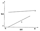
図5は、データ書込時におけるデータ書込電流の方向と磁界方向との関係を示す図である。図5を参照して、横軸で示される磁界Hxは、ディジット線DLを流れるデータ書込電流によって生じる磁界H(DL)を示している。一方、縦軸に示される磁界Hyは、ビット線BLを流れるデータ書込電流によって生じる磁界H(BL)を示している。
【0014】
自由磁化膜VLに記憶される磁界方向は、磁界H(DL)とH(BL)の和が図中に示されるアステロイド特性線の外側の領域に達する場合においてのみ、新たに書込まれる。すなわち、アステロイド特性線の内側の領域に相当する磁界が印加された場合においては、自由磁化膜VLに記憶される磁界方向は更新されない。したがって、トンネル磁気抵抗素子TMRの記憶データを書込動作によって更新するためには、ディジット線DLとビット線BLとの両方に電流を流す必要がある。トンネル磁気抵抗素子TMRに一旦記憶された磁界方向すなわち記憶データは、新たなデータ書込が実行されるまでの間不揮発的に保持される。
【0015】
データ読出時は、図6に示すように、ワード線WLが選択レベルの「H」レベルにされてアクセストランジスタATRが導通し、ビット線BLからトンネル磁気抵抗素子TMRおよびアクセストランジスタATRを介して接地電位VSSのラインに電流Isが流れる。この電流Isの値は、トンネル磁気抵抗素子TMRの抵抗値に応じて変化する。したがって、この電流Isの値を検知することにより、トンネル磁気抵抗素子TMRの記憶データを読出すことができる。
【0016】
図1に戻って、行デコーダ2は、アドレス信号ADDに含まれる行アドレス信号RAに従ってメモリアレイ1の複数行のうちのいずれかの行を選択する。ドライブ回路3は、データ書込時は行デコーダ2によって選択された行のディジット線DLに書込電流を流し、データ読出時は行デコーダ2によって選択された行のワード線WLを選択レベルの「H」レベルに立上げる。ディジット線電流制御回路4は、ディジット線DLの書込電流を制御する。
【0017】
列デコーダ5は、アドレス信号ADDに含まれる列アドレス信号CAに従って、メモリアレイ1の複数のメモリブロックMBのうちのいずれかのメモリブロックMBを選択するとともに、選択したメモリブロックMBの複数の列のうちのいずれかi個の列を選択する。読出・書込制御回路6,7は、データ書込時は、外部から与えられた書込データ信号D1〜Diに従って、列デコーダ5によって選択されたi個の列に対応するi本のビット線BLの各々に書込電流を流し、i個のメモリセルMCの各々にデータ信号を書込む。また、読出・書込制御回路6,7は、データ読出時は、列デコーダ5によって選択されたi個の列に対応するi本のビット線BLの各々に流れる電流Isを検出し、検出結果に応じた論理のデータ信号Q1〜Qiを外部に出力する。コントロール回路8は、外部コマンド信号CMDに従ってMRAMデバイス全体を制御する。
【0018】
以下、この発明の特徴となるビット線BLおよびディジット線DLの書込電流制御方法について説明する。図7は、1つのメモリブロックMBのデータ書込に関連する部分を示す回路ブロック図である。図7において、メモリブロックMBは、ビット線BLの延在方向に2つのサブブロックMBaとMBbに分割されている。各ビット線BLは、サブブロックMBaに属する部分BLaとサブブロックMBbに属する部分BLbとに分割される。2つのサブブロックMBaとMBbの間にビット線ドライバ10が配置され、2つのサブブロックMBa,MBbの両側にビット線ドライバ11,12が配置される。
【0019】
メモリブロックMBは、ディジット線DLの延在する方向に4つの領域A,B,C,Dに分割されている。データ書込時は、メモリブロックMBの複数行のうちのいずれかの行と、メモリブロックMBの複数列のうちのいずれかi個(ここでは、8個とする)の列とが選択される。列は、予め2つずつグループ化されており、4つの領域A〜Dで2つずつ選択される。選択された行のディジット線DLと、そのディジット線DLが属するサブブロック(図ではMBa)の選択された各列のビット線BLaとの各々に書込電流が流される。
【0020】
4つの領域A〜Dに対応してそれぞれ定電流回路13〜16が配置される。定電流回路13〜16の出力電流の各々は、ビット線ドライバ10〜12に与えられる。定電流回路13〜16の出力電流は、ビット線ドライバ10〜12を介して、それぞれ領域A〜Dで選択されたビット線BLaまたはBLbに流される。ビット線ドライバ10〜12は、列デコーダ5によって選択された8本のビット線BLに、それぞれ外部データ信号D1〜D8に応じた方向の書込電流を流す。定電流回路13〜16およびビット線ドライバ10〜12は、図1の読出・書込制御回路6,7に含まれる。
【0021】
2つのサブブロックMBa,MBbに対応してそれぞれディジット線ドライバ17,18が配置され、複数のディジット線DLに共通に定電流回路19が配置される。ディジット線DLの一方端は定電流回路19の出力電流を受け、その他方端はディジット線ドライバ17または18に接続される。ディジット線ドライバ17,18は、行デコーダ2によって選択された行のディジット線DLの他方端を接地してそのディジット線DLに書込電流を流す。ディジット線ドライバ17,18は図1のドライブ回路3に含まれ、定電流回路19は、図1のディジット線電流制御回路4に含まれる。
【0022】
図8は、領域Aにおけるビット線ドライバ10〜12の構成を示す回路図である。図8において、各列に対応して選択信号φS1〜φS4を伝達するための4本の信号線が配置され、ビット線ドライバ10は、各列に対応して設けられた論理ゲート20,21、PチャネルMOSトランジスタ22およびNチャネルMOSトランジスタ23を含む。論理ゲート20は、活性化信号φE0が活性化レベルの「H」レベルにされ、かつ対応の列の選択信号φS1,φS2がともに「L」レベルにされた場合に、活性化レベルの「L」レベルを出力する。論理ゲート21は、活性化信号φE0が活性化レベルの「H」レベルにされ、かつ対応の列の選択信号φS3,φS4がともに「H」レベルにされた場合に、活性化レベルの「H」レベルを出力する。PチャネルMOSトランジスタ22のソースは、定電流回路13の出力ノードに接続され、そのドレインはビット線BLa,BLbの一方端(ビット線BLの中央)に接続され、そのゲートは論理ゲート20の出力信号を受ける。NチャネルMOSトランジスタ22のドレインはビット線BLa,BLbの一方端に接続され、そのソースは接地電位VSSのラインに接続され、そのゲートは論理ゲート21の出力信号を受ける。
【0023】
ビット線ドライバ11は、各列に対応して設けられた論理ゲート24,25、PチャネルMOSトランジスタ26およびNチャネルMOSトランジスタ27を含む。論理ゲート24は、活性化信号φE1が活性化レベルの「H」レベルにされ、かつ対応の列の選択信号φS1,φS2がそれぞれ「L」レベルおよび「H」レベルにされた場合に、活性化レベルの「L」レベルを出力する。論理ゲート25は、活性化信号φE1が活性化レベルの「H」レベルにされ、かつ対応の列の選択信号φS3,φS4がそれぞれ「H」レベルおよび「L」レベルにされた場合に、活性化レベルの「H」レベルを出力する。PチャネルMOSトランジスタ26のソースは、定電流回路13の出力ノードに接続され、そのドレインはビット線BLaの他方端(ビット線BLの一方端)に接続され、そのゲートは論理ゲート24の出力信号を受ける。NチャネルMOSトランジスタ27のドレインはビット線BLaの他方端に接続され、そのソースは接地電位VSSのラインに接続され、そのゲートは論理ゲート27の出力信号を受ける。
【0024】
ビット線ドライバ12は、各列に対応して設けられた論理ゲート28,29、PチャネルMOSトランジスタ30およびNチャネルMOSトランジスタ31を含む。論理ゲート28は、活性化信号φE2が活性化レベルの「H」レベルにされ、かつ対応の列の選択信号φS1,φS2がそれぞれ「H」レベルおよび「L」レベルにされた場合に、活性化レベルの「L」レベルを出力する。論理ゲート29は、活性化信号φE2が活性化レベル「H」レベルにされ、かつ対応の列の選択信号φS3,φS4がそれぞれ「L」レベルおよび「H」レベルにされた場合に、活性化レベルの「H」レベルを出力する。PチャネルMOSトランジスタ30のソースは、定電流回路13の出力ノードに接続され、そのドレインはビット線BLbの他方端(ビット線BLの他方端)に接続され、そのゲートは論理ゲート28の出力信号を受ける。NチャネルMOSトランジスタ31のドレインはビット線BLbの他方端に接続され、そのソースは接地電位VSSのラインに接続され、そのゲートは論理ゲート29の出力信号を受ける。
【0025】
たとえば、図8の上側の列のビット線BLaにおいて図中左側から右側に電流を流す場合は、活性化信号φE0,φE1を「H」レベルにし、上側の列の選択信号φS1〜φS4をそれぞれ「L」レベル、「H」レベル、「H」レベル、「H」レベルにする。これにより、上側の列のPチャネルMOSトランジスタ26およびNチャネルMOSトランジスタ23が導通し、定電流回路13の出力電流がPチャネルMOSトランジスタ26、ビット線BLaおよびNチャネルMOSトランジスタ23を介して接地電位VSSのラインに流れる。
【0026】
また、図8の上側の列のビット線BLbにおいて図中右側から左側に電流を流す場合は、活性化信号φE0,φE2を「H」レベルにし、上側の列の選択信号φS1〜φS4をそれぞれ「H」レベル、「L」レベル、「H」レベル、「H」レベルにする。これにより、上側の列のPチャネルMOSトランジスタ30およびNチャネルMOSトランジスタ23が導通し、定電流源13の出力電流がPチャネルMOSトランジスタ30、ビット線BLbおよびNチャネルMOSトランジスタ23を介して接地電位VSSのラインに流れる。このようにして、領域Aのいずれのビット線についても所望の方向の電流を流すことができる。
【0027】
他の領域B〜Dにおけるビット線ドライバ10〜12の構成も、領域Aにおけるビット線ドライバ10〜12と同じ構成である。ただし、領域BのPチャネルMOSトランジスタ22,26,30のソースは定電流回路14の出力電流を受け、領域CのPチャネルMOSトランジスタ22,26,30のソースは定電流回路15の出力電流を受け、領域DのPチャネルMOSトランジスタ22,26,30のソースは定電流回路16の出力電流を受ける。
【0028】
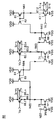
図9は、定電流回路13の要部を示す回路図である。図9において、この定電流回路13は、キャパシタ35、PチャネルMOSトランジスタ36,37およびNチャネルMOSトランジスタ38を含む。キャパシタ35は、定電流回路13の出力ノードN36と接地電位VSSのラインとの間に接続され、ノードN36の電位を安定化させる。PチャネルMOSトランジスタ36,37は、それぞれ電源電位VDDのラインとノードN36,N37との間に接続され、それらのゲートはともにノードN37に接続される。PチャネルMOSトランジスタ36,37は、カレントミラー回路を構成する。PチャネルMOSトランジスタ36と37のサイズ比はxに設定されており、PチャネルMOSトランジスタ37に流れる基準電流Irblのx倍の電流Irbl・xがPチャネルMOSトランジスタ36に流れる。トンネル磁気抵抗素子TMRの自由磁化膜VLの磁化方向を反転させるために必要な書込電流は自由磁化膜VLの温度が高いほど小さくなるので、基準電流Irblは温度上昇に従って減少するように制御される。その制御方法については後に詳述する。
【0029】
NチャネルMOSトランジスタ38は、出力ノードN36と接地電位VSSのラインとの間に接続され、そのゲートは信号ENLを受ける。NチャネルMOSトランジスタ36は、PチャネルMOSトランジスタ38と同じ電流駆動能力を有する。信号ENLは、活性化信号φE1〜φE3が「H」レベルに立ち上げられるときに所定時間だけ「H」レベルにされる。これにより、定電流Irbl・xがNチャネルMOSトランジスタ38を介して接地電位VSSのラインに流出し、ビット線BLの電位VBLが上昇しすぎるのを防止する。
【0030】
図10は、定電流回路13の他の部分を示す回路図である。図10において、この定電流回路13は、さらに、PTAT(Proportional To Absolute temperature)電流発生回路40および温度依存性電流発生回路46を含む。PTAT電流発生回路40は、PチャネルMOSトランジスタ41,42、NチャネルMOSトランジスタ43,44および抵抗素子45を含む。PチャネルMOSトランジスタ41,42は、それぞれ電源電位VDDのラインとノードN41,N42との間に接続され、それらのゲートはノードN41に接続される。NチャネルMOSトランジスタ43および抵抗素子45はノードN41と接地電位VSSのラインとの間に直列接続され、NチャネルMOSトランジスタ44はノードN42と接地電位VSSのラインとの間に接続され、NチャネルMOSトランジスタ43,44のゲートはともにノードN42に接続される。PチャネルMOSトランジスタ41に流れる電流Ipは次式で表わされる。
【0031】
Ip=(kT/q)(1/R1)ln(W2/W1)(W4/W3)
ただし、kはボルツマン定数、Tは絶対温度、qは電子の電荷、R1は抵抗素子45の抵抗値、W1〜W4はそれぞれMOSトランジスタ44,43,41,42のゲート幅である。
【0032】
したがって、PTAT電流Ipは、図11に示すように、絶対温度Tに比例した値になる。また、PTAT電流Ipのレベルを調整するためには、R1,W1〜W4を調整すればよい。
【0033】
図10に戻って、温度依存性電流発生回路46は、抵抗素子47,48、PチャネルMOSトランジスタ49〜52およびNチャネルMOSトランジスタ53〜55を含む。抵抗素子47およびPチャネルMOSトランジスタ49は電源電位VDDのラインとノードN49の間に直列接続され、抵抗素子48およびPチャネルMOSトランジスタ50は電源電位VDDのラインとノードN50の間に直列接続され、PチャネルMOSトランジスタ49,50のゲートはともにノードN49に接続される。NチャネルMOSトランジスタ53,54は、それぞれノードN49,N50と接地電位VSSのラインとの間に接続され、それらのゲートはともにノードN42に接続される。PチャネルMOSトランジスタ51,52は、それぞれ電源電位VDDのラインとノードN50,N52との間に接続され、それらのゲートはともにノードN50に接続される。NチャネルMOSトランジスタ55は、ノードN52と接地電位VSSのラインとの間に接続され、そのゲートはノードN52に接続される。
【0034】
抵抗素子47と48は、互いに異なる抵抗材料で形成されており、互いに異なる温度依存性を有する。抵抗素子47,48の抵抗値R2,R3の大小関係は、ある温度で逆転する。R2≧R3のときは、抵抗素子47およびMOSトランジスタ49,53の経路と抵抗素子48およびMOSトランジスタ50,54の経路とに同じ値の電流が流れ、It=0となる。R2<R3のときは、NチャネルMOSトランジスタ53と54に同じ値の電流を流すためにPチャネルMOSトランジスタ51に電流Itが流れる。この電流Itは、PチャネルMOSトランジスタ52およびNチャネルMOSトランジスタ55にも流れる。電流Itは、図11に示すように、ある温度で発生し、温度上昇に従って増加する。電流Itの温度依存性は、電流Ipの温度依存性よりも大きい。発生温度、温度上昇の程度は、抵抗素子47,48の抵抗材料および抵抗値により調整可能である。
【0035】
図12は、定電流回路13のさらに他の部分を示す回路図である。図12において、定電流回路13は基準電流発生回路60を含み、基準電流発生回路60はPチャネルMOSトランジスタ61,62,63.1〜63.n,64,65,66.1〜66.mおよびNチャネルMOSトランジスタ67.1〜67.q,68〜73を含む。ただし、n,m,qの各々は自然数であり、n>mである。PチャネルMOSトランジスタ61,62は、それぞれ電源電位VDDのラインとノードN61,N62との間に接続され、それらのゲートはノードN61に接続される。PチャネルMOSトランジスタ61,62は、カレントミラー回路を構成する。
【0036】
NチャネルMOSトランジスタ67.1〜67.qは、ノードN61と接地電位VSSのラインとの間に接続され、それらのゲートは図10のノードN52の電位Vtを受ける。NチャネルMOSトランジスタ68,69は、それぞれノードN62,63と接地電位VSSのラインとの間に接続され、それらのゲートはともにノードN62に接続される。NチャネルMOSトランジスタ68と69は、カレントミラー回路を構成する。したがって、MOSトランジスタ61,62,68,69の各々には、温度依存性電流Itのq倍の電流It・qが流れる。
【0037】
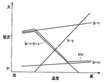
PチャネルMOSトランジスタ63.1〜63.nは、電源電位VDDのラインとのノードN63との間に並列接続され、それらのゲートは図10のノードN41の電位Vpを受ける。NチャネルMOSトランジスタ70,71は、それぞれノードN63,N64と接地電位VSSのラインとの間に接続され、それらのゲートはともにノードN63に接続される。NチャネルMOSトランジスタ70,71は、カレントミラー回路を構成する。PチャネルMOSトランジスタ64,65は、それぞれ電源電位VDDのラインとノードN64,N65の間に接続され、それらのゲートはともにノードN64に接続される。PチャネルMOSトランジスタ64,65は、カレントミラー回路を構成する。PチャネルMOSトランジスタ63.1〜63.nには、PTAT電流Ipのn倍の電流Ip・nが流れる。電流Ip・nのうちのIt・qはNチャネルMOSトランジスタ69に流れる。したがって、MOSトランジスタ70,71,64,65の各々には、電流(Ip・n−It・q)が流れる。この電流(Ip・n−It・q)は、図13に示すように、温度上昇に従って減少する。
【0038】
図12に戻って、PチャネルMOSトランジスタ66.1〜66.mは、電源電位VDDのラインとノードN65との間に並列接続され、それらのゲートはともに図10のノードN41の電位Vpを受ける。NチャネルMOSトランジスタ72,73は、それぞれノードN65,N37と接地電位VSSのラインとの間に接続され、それらのゲートはノードN65に接続される。NチャネルMOSトランジスタ72,73は、カレントミラー回路を構成する。PチャネルMOSトランジスタ66.1〜66.mには、PTAT電流Ipのm倍の電流Ip・mが流れる。したがって、NチャネルMOSトランジスタ72,73の各々に流れる電流Irblは、Ip・m+(Ip・n−It・q)となる。Ip・mは、電流Irblがデッドロックすなわち0になることを防止するための電流である。電流Irblは、図13に示すように、温度上昇に従って減少し、0にならない。この電流Irblは図9のPチャネルMOSトランジスタ37に流れ、定電流回路13の出力電流はIrbl・xとなる。
【0039】
図14は、ディジット線DLの電流制御に関連する部分の構成を示す回路図である。図14を参照して、図7の定電流回路19は、キャパシタ75およびPチャネルMOSトランジスタ76,77を含む。キャパシタ75は、定電流回路19の出力ノードN76と接地電位VSSのラインとの間に接続され、ノードN76の電位を安定化させる。PチャネルMOSトランジスタ76,77は、それぞれ電源電位VDDのラインとノードN76,N77の間に接続され、そのゲートはともにノードN77に接続される。PチャネルMOSトランジスタ76,77は、カレントミラー回路を構成する。PチャネルMOSトランジスタ76と77のサイズ比はyに設定されており、PチャネルMOSトランジスタ77に流れる基準電流Irdlのy倍の電流Irdl・yがPチャネルMOSトランジスタ76に流れる。
【0040】
ノードN77は、図15の基準電流発生回路78のNチャネルMOSトランジスタ73のドレインに接続される。基準電流発生回路78は、図12の基準電流発生回路60と同じ構成である。ただし、PチャネルMOSトランジスタ66.1〜66.mはPチャネルMOSトランジスタ66.1〜66.rで置換され、PチャネルMOSトランジスタ63.1〜63.nはPチャネルMOSトランジスタ63.1〜63.sで置換され、NチャネルMOSトランジスタ67.1〜67.qはNチャネルMOSトランジスタ67.1〜67.tで置換されている。ここで、r,s,qの各々は自然数である。したがって、基準電流Irdlは、Ip・r+(Ip・s−It・t)となり、温度上昇に従って減少し、0にならない。なお、図10のPTAT電流発生回路40および温度依存性電流発生回路46は、定電流回路13,19に共通に設けてもよいし、定電流回路13,19のそれぞれに設けてもよい。
【0041】
図14に戻って、メモリブロックMBに含まれる複数のディジット線DLの一方端は、ともに定電流回路19の出力ノードN76に接続される。各ディジット線DLに対応して、NチャネルMOSトランジスタ80およびANDゲート81が設けられる。NチャネルMOSトランジスタ80およびANDゲート81は、図7のディジット線ドライバ17,18に含まれている。各NチャネルMOSトランジスタ80は、対応のディジット線DLの他方端と接地電位VSSのラインとの間に接続され、そのゲートは対応のANDゲート81の出力信号を受ける。ANDゲート81の一方入力ノードは活性化信号ENDLを受け、その他方入力ノードN81は行デコーダ2に接続される。
【0042】
行デコーダ2は、データ書込時に、行アドレス信号RAに従って複数行のうちのいずれかの行を選択し、その行のノードN81の電位を「L」レベルから「H」レベルに立上げる。活性化信号ENDLが活性化レベルの「H」レベルに立上げられると、行デコーダ2によって選択された行のANDゲート81の出力信号が「H」レベルになり、その行のNチャネルMOSトランジスタ80が導通する。これにより、電源電位VDDのラインからPチャネルMOSトランジスタ76、その行のディジット線DLおよび導通したNチャネルMOSトランジスタ80を介して接地電位VSSのラインに書込電流が流れる。
【0043】
図16は、図7〜図15で示したビット線BLおよびディジット線DLの電流制御方法を示すタイムチャートである。図16において、クロック信号CLKのある立上がりエッジ(時刻t1)において外部コマンド信号CMDに含まれる信号CS,WEがともに「H」レベルにされていると、図14の活性化信号ENDLが活性化レベルの「H」レベルに立上げられ、選択された行のディジット線DLに書込電流IDLが流れる。
【0044】
また、図9の信号ENLが活性化レベルの「H」レベルに立上げられてNチャネルMOSトランジスタ38が導通し、定電流回路13の出力ノードN36の電位VDが低下する。次いで時刻t2において、図9の活性化信号φE0〜φE2のうちのいずれか2つの信号が活性化レベルの「H」レベルに立上げられる。この時点では、信号ENLがまだ「H」レベルにされているので、PチャネルMOSトランジスタ36に流れる定電流Irbl・xはNチャネルMOSトランジスタ38を介して接地電位VSSのラインに流出し、ビット線BLに電流は流れない。次いで信号ENLが「H」レベルから「L」レベルに立下げられると、定電流Irbl・xがビット線ドライバ10〜12を介して2本のビット線BLに分流される。
【0045】
ビット線BLに電流IBL=Irbl・x/2が流されるとビット線BLの電位VBLは上昇するが、その前の期間にNチャネルMOSトランジスタ38を導通させて定電流回路13の出力ノードN36の電位VDを低下させているので、ビット線BLの電位VBLが上昇しぎるのを防止することができる。次に、時刻t3において信号φE0〜φE2が「L」レベルに立下げられてビット線BLの電流IBLが遮断され、さらに時刻t4において信号ENDLが「L」レベルに立下げられてディジット線DLの電流IDLが遮断される。
【0046】
この実施の形態では、データ書込時にビット線BLに流される書込電流を生成するために定電流回路13〜16を設けたので、電源電位VDDの変動などの影響を受けることなく、安定した書込電流を生成することができ、安定したデータ書込みを行うことができる。
【0047】
また、ビット線BLに書込電流を流す前に定電流回路13〜16の出力電流を一旦接地電位VSSのラインに流出させるので、ビット線BLの電位VBLが上昇しすぎることを防止することができる。したがって、メモリセルMCに高電圧が印加されて破壊されることを防止することができ、信頼性の向上を図ることができる。
【0048】
また、データ書込時にディジット線DLに流される書込電流を生成するために定電流回路19を設けたので、電源電位VDDの変動などの影響を受けることなく、安定した書込電流を生成することができ、安定したデータ書込みを行うことができる。
【0049】
また、定電流回路19を設けたので、電源投入時に大きな充電電流がディジット線DLに流れるのを防止することができる。このため、システムの電源にノイズが発生するのを防止することができ、システムの性能の向上を図ることができる。
【0050】
また、定電流回路13〜16,19の出力電流は温度上昇に伴って低下するので、必要以上に大きな書込電流が流れるのを防止することができ、消費電流の低減化および信頼性の向上を図ることができる。
【0051】
また、定電流回路13〜16,19の出力電流が温度上昇に伴って低下するが、デッドロックすることはない。したがって、信頼性を担保することができる。なお、定電流回路13〜16,19の出力電流を温度以外のパラメータに従って制御してもよい。
【0052】
なお、この実施の形態では、メモリブロックMBを4つの領域A〜Dに分割し、4つの領域A〜Dから2つずつ8個のメモリセルMCを選択したが、メモリブロックMBを2つの領域に分割して4つずつ選択してもよいし、メモリブロックMBを8つの領域に分割して1つずつ選択してもよい。また、16個のメモリセルMCを同時に選択する場合は、メモリブロックMBを16の領域に分割して1つずつ選択してもよいし、メモリブロックMBを8つの領域に分割して2つずつ選択してもよいし、メモリブロックMBを4つの領域に分割して4つずつ選択してもよいし、メモリブロックMBを2つの領域に分割して8つずつ選択してもよい。いずれの場合も、1つの領域に対応して1つの定電流回路が設けられる。
【0053】
また、この実施の形態では、1本のディジット線DLと8本のビット線BLとの各々に書込電流を流して8個のメモリセルMCにデータを書込んだが、逆に、1本のビット線BLと8本のディジット線DLとの各々に書込電流を流して8個のメモリセルMCにデータを書込んでもよい。この場合は、メモリブロックMBをビット線BLの延在方向に4つの領域に分割し、4つの領域から2本ずつディジット線DLを選択し、各領域に対応してディジット線DL用の定電流回路を設けるとよい。
【0054】
また、この実施の形態では、定電流回路13〜16は常時活性化されていたが、ビット線ドライバ10〜12を活性化させてから定電流回路13〜16を活性化させてもよい。たとえば図17に示すように、電源電位VDDのラインとPチャネルMOSトランジスタ36のソースとの間に、ビット線ドライバ10〜12が活性化されたことに応じて導通するスイッチ82を介挿するとよい。たとえば活性化信号φE0〜φE2の論理和信号をスイッチ82の制御信号φEとして使用すると良い。
【0055】
また、図18は、冗長方式が採用されたMRAMデバイスにこの発明が適用された例を示すブロック図である。このMRAMデバイスでは、4つの領域A〜Dから2本ずつ8本のビット線BLが選択される。4つの領域A〜Dの各々に2本1組でスペアビット線SBLが設けられる。同時に選択される2本のビット線BLのうちの少なくとも1本のビット線BLが不良である場合は、その2本1組のビット線BLは同じ領域内の2本1組のスペアビット線SBLと置換される。図19に示すように、2本1組のビット線BLと2本1組のスペアビット線SBLには、同じ定電流回路(図では13)から書込電流が供給される。
【0056】
また、図20は、冗長方式が採用されたMRAMデバイスにこの発明が適用された他の例を示すブロック図である。このMRAMデバイスでは、4本1組のビット線BLが同時に選択される。4本のビット線BLには、それぞれ定電流回路13〜16の出力電流が流される。4本1組のスペアビット線SBLが設けられる。同時に選択される4本のビット線BLのうちの少なくとも1本のビット線BLが不良の場合は、その4本1組のビット線BLは4本1組のスペアビット線SBLと置換される。図21に示すように、4本1組のビット線BLのうちの1本のビット線BLと、そのビット線BLに対応するスペアビット線SBLとには、同じ定電流回路(たとえば13)から書込電流が供給される。
【0057】
今回開示された実施の形態はすべての点で例示であって制限的なものではないと考えられるべきである。本発明の範囲は上記した説明ではなくて特許請求の範囲によって示され、特許請求の範囲と均等の意味および範囲内でのすべての変更が含まれることが意図される。
【0058】
【発明の効果】
以上のように、この発明に係る薄膜磁性体記憶装置では、複数行複数列に配置され、各々が磁気的にデータを記憶する複数のメモリセルと、それぞれ複数列に対応して設けられた複数のビット線とを含むメモリブロックとが設けられる。メモリブロックは、複数のビット線の延在方向に2つのサブブロックに分割されるとともに、複数のビット線と直交する方向に複数の領域に分割される。複数のビット線は、2つのサブブロックの両方を通るように配置される。データ書込時には、各領域から少なくとも1つのビット線が選択される。この薄膜磁性体記憶装置は、さらに、それぞれ複数の領域に対応して設けられた複数の電流源と、複数のビット線に並行に設けられ、それぞれ複数の電流源に接続された複数の電源線とを備える。領域の数と電流源の数と電源線の数は同一である。この薄膜磁性体記憶装置は、さらに、各領域に対応して設けられて対応の電源線に接続され、対応する領域の選択された各ビット線に対応の電流源の電流を書込データに応じた方向に流す書込回路を備える。書込回路は、各ビット線に対応して設けられ、対応するビット線の一方端に接続された第1のビット線ドライバと、各ビット線に対応して設けられ、対応するビット線の他方端に接続された第2のビット線ドライバと、各ビット線に対応して前記2つのサブブロックの間に設けられ、対応するビット線に接続された第3のビット線ドライバとを含み、選択された各ビット線に対応する第1または第2のビット線ドライバと第3のビット線ドライバとの間に対応の電流源の電流を流す。したがって、電源電圧が変動しても安定した書込電流をビット線に流すことができ、安定したデータ書込みを行うことができる。
【図面の簡単な説明】
【図1】 この発明の一実施の形態によるMRAMデバイスの全体構成を示すブロック図である。
【図2】 図1に示したメモリブロックの構成を示す回路図である。
【図3】 図2に示したメモリセルの構成を示す回路図である。
【図4】 図3に示したメモリセルのデータ書込方法を説明するための図である。
【図5】 図3に示したメモリセルのデータ書込方法を説明するための他の図である。
【図6】 図3に示したメモリセルのデータ読出方法を説明するための図である。
【図7】 図1に示したMRAMデバイスのデータ書込に関連する部分の構成を示す回路ブロック図である。
【図8】 図7に示したビット線ドライバの構成を示す回路図である。
【図9】 図7に示した定電流回路13の要部を示す回路図である。
【図10】 図7に示した定電流回路13に含まれるPTAT電流発生回路および温度依存性電流発生回路の構成を示す回路図である。
【図11】 図10に示したPTAT電流発生回路および温度依存性電流発生回路の動作を示す図である。
【図12】 図7に示した定電流回路13に含まれる基準電流発生回路の構成を示す回路図である。
【図13】 図12に示した基準電流発生回路の動作を示す図である。
【図14】 図7に示したディジット線ドライバおよび定電流回路19の要部を示す回路図である。
【図15】 図7に示した定電流回路19に含まれる基準電流発生回路の構成を示す回路図である。
【図16】 図1〜図15に示したMRAMデバイスのデータ書込動作を示すタイムチャートである。
【図17】 この実施の形態の変更例を示す回路図である。
【図18】 この実施の形態の他の変更例を示す回路ブロック図である。
【図19】 図18に示したビット線ドライバの構成を示す回路図である。
【図20】 この実施の形態の他の変更例を示す回路ブロック図である。
【図21】 図20に示したビット線ドライバの構成を示す回路図である。
【符号の説明】
1 メモリアレイ、2 行デコーダ、3 ドライブ回路、4 ディジット線電流制御回路、5 列デコーダ、6,7 読出・書込制御回路、8 コントロール回路、MC メモリセル、BL ビット線、SBL スペアビット線、WL ワード線、DL ディジット線、MB メモリブロック、TMR トンネル磁気抵抗素子、ATR アクセストランジスタ、VL 自由磁化膜、TB トンネル絶縁膜、FL 固定磁化膜、10〜12 ビット線ドライバ、13〜16,19 定電流回路、17,18 ディジット線ドライバ、MBa,MBb サブブロック、20,21,24,25,28,29 論理ゲート、22,26,30,36,37,41,42,49〜52,61〜66,76,77 PチャネルMOSトランジスタ、23,27,31,38,43,44,53〜55,67〜73,80 NチャネルMOSトランジスタ、35,75 キャパシタ、40 PTAT電流発生回路、45,47,48 抵抗素子、46 温度依存性電流発生回路、60,78 基準電流発生回路、81 ANDゲート、82 スイッチ。[0001]
BACKGROUND OF THE INVENTION
The present invention relates to a thin film magnetic memory device, and more particularly to a randomly accessible thin film magnetic memory device including a memory cell having a magnetic tunnel junction (MTJ).
[0002]
[Prior art]
An MRAM (Magnetic Random Access Memory) device has attracted attention as a storage device that can store nonvolatile data with low power consumption. An MRAM device is a storage device that performs non-volatile data storage using a plurality of thin film magnetic bodies formed in a semiconductor integrated circuit and allows random access to each of the thin film magnetic bodies.
[0003]
In particular, in recent years, it has been announced that the performance of MRAM devices will be dramatically improved by using a tunnel magnetoresistive element using a magnetic tunnel junction as a memory cell. For example, Non-Patent
[0004]
[Non-Patent Document 1]
“A 10ns Read and Write Non-Volatile Memory Array Using a Magnetic Tunnel Junction and FET Switch in each Cell”, ISSCC Digest of Technical Papers, TA7.2, Feb. 2000
[0005]
[Problems to be solved by the invention]
In such an MRAM device, in order to write a data signal to the tunnel magnetoresistive element, it is necessary to pass a predetermined write current through each of the digit line and the bit line. However, the conventional MRAM device has a problem that the writing current fluctuates due to fluctuations in the power supply voltage and the like, and stable data writing cannot be performed.
[0006]
Therefore, a main object of the present invention is to provide a thin film magnetic memory device capable of performing stable data writing.
[0007]
[Means for Solving the Problems]
The thin film magnetic memory device according to the present invention is Arranged in multiple rows and multiple columns, Each is magnetically T Multiple memory cells to store, multiple each Column Multiple corresponding to And a memory block including a bit line. The memory block is divided into two sub-blocks in the extending direction of the plurality of bit lines, and is divided into a plurality of regions in a direction orthogonal to the plurality of bit lines. The plurality of bit lines are arranged to pass through both of the two sub blocks. At the time of data writing, at least one bit line is selected from each region. The thin-film magnetic memory device further includes a plurality of current sources provided corresponding to the plurality of regions, and a plurality of power supply lines provided in parallel to the plurality of bit lines and respectively connected to the plurality of current sources. With. The number of regions, the number of current sources, and the number of power supply lines are the same. The thin film magnetic memory device is further provided corresponding to each region and connected to a corresponding power supply line, and the current of the current source corresponding to each selected bit line in the corresponding region is determined according to the write data. A writing circuit for flowing in the opposite direction. The write circuit is provided corresponding to each bit line, and is provided corresponding to each bit line, the first bit line driver connected to one end of the corresponding bit line, and the other of the corresponding bit lines A second bit line driver connected to the end and a third bit line driver provided between the two sub-blocks corresponding to each bit line and connected to the corresponding bit line; A current of a corresponding current source is caused to flow between the first or second bit line driver and the third bit line driver corresponding to each bit line .
[0008]
DETAILED DESCRIPTION OF THE INVENTION
FIG. 1 is a block diagram showing the overall configuration of an MRAM device according to an embodiment of the present invention. 1, the MRAM device includes a
[0009]
The
[0010]
Each memory cell MC includes a tunnel magnetoresistive element TMR and an access transistor (N channel MOS transistor) ATR as shown in FIG. Tunneling magneto-resistance element TMR and access transistor ATR are connected in series between corresponding bit line BL and the ground potential VSS line, and the gate of access transistor ATR is connected to corresponding word line WL. Tunneling magneto-resistance element TMR is an element whose electric resistance value changes according to the logic of stored data.
[0011]
That is, as shown in FIG. 4, tunnel magnetoresistive element TMR includes fixed magnetization film FL, tunnel insulating film TB, and free magnetization film VL stacked between electrode EL and bit line BL. Each of the fixed magnetization film FL and the free magnetization film VL is composed of a ferromagnetic film. The magnetization direction of the fixed magnetization film FL is fixed in one direction. The magnetization direction of free magnetic film VL is written in one of one direction and the other direction. When the magnetization directions of the fixed magnetization film FL and the free magnetization film VL are the same, the resistance value of the tunnel magnetoresistive element TMR becomes a relatively large value, and when the magnetization directions of the two are opposite, the tunnel magnetoresistive element TMR The electric resistance value is relatively small. The two-stage resistance values of tunneling magneto-resistance element TMR are associated with
[0012]
At the time of data writing, as shown in FIG. 4, word line WL is set to the “L” level of the non-selection level and access transistor ATR is made non-conductive, and writing is performed to each of bit line BL and digit line DL. A current flows. The magnetization direction of free magnetic film VL is determined by the combination of the directions of the write currents flowing through bit line BL and digit line DL.
[0013]
FIG. 5 is a diagram showing the relationship between the direction of the data write current and the magnetic field direction during data writing. Referring to FIG. 5, a magnetic field Hx indicated by the horizontal axis indicates a magnetic field H (DL) generated by a data write current flowing through digit line DL. On the other hand, the magnetic field Hy indicated on the vertical axis indicates the magnetic field H (BL) generated by the data write current flowing through the bit line BL.
[0014]
The magnetic field direction stored in the free magnetic film VL is newly written only when the sum of the magnetic fields H (DL) and H (BL) reaches a region outside the asteroid characteristic line shown in the drawing. That is, when a magnetic field corresponding to the area inside the asteroid characteristic line is applied, the magnetic field direction stored in the free magnetic film VL is not updated. Therefore, in order to update the storage data of tunneling magneto-resistance element TMR by the write operation, it is necessary to pass a current through both digit line DL and bit line BL. The magnetic field direction once stored in tunneling magneto-resistance element TMR, that is, the stored data is held in a nonvolatile manner until new data writing is executed.
[0015]
At the time of data reading, as shown in FIG. 6, word line WL is set to the “H” level of the selection level and access transistor ATR is turned on, and grounded from bit line BL through tunneling magneto-resistance element TMR and access transistor ATR. A current Is flows through the line of the potential VSS. The value of this current Is changes according to the resistance value of tunneling magneto-resistance element TMR. Therefore, the data stored in tunneling magneto-resistance element TMR can be read by detecting the value of current Is.
[0016]
Returning to FIG. 1, the row decoder 2 selects one of the plurality of rows of the
[0017]
The
[0018]
Hereinafter, a write current control method for bit line BL and digit line DL, which is a feature of the present invention, will be described. FIG. 7 is a circuit block diagram showing a portion related to data writing in one memory block MB. In FIG. 7, the memory block MB is divided into two sub-blocks MBa and MBb in the extending direction of the bit line BL. Each bit line BL is divided into a part BLa belonging to sub-block MBa and a part BLb belonging to sub-block MBb.
[0019]
Memory block MB is divided into four areas A, B, C, and D in the direction in which digit line DL extends. At the time of data writing, any one of the plurality of rows of the memory block MB and any i (here, eight) columns of the plurality of columns of the memory block MB are selected. . Two columns are grouped in advance, and two columns are selected in each of the four areas A to D. A write current is supplied to the digit line DL of the selected row and the bit line BLa of each selected column of the sub-block (MBa in the figure) to which the digit line DL belongs.
[0020]
Constant
[0021]
[0022]
FIG. 8 is a circuit diagram showing the configuration of the
[0023]
[0024]
[0025]
For example, in the case where a current flows from the left side to the right side in FIG. 8 on the bit line BLa in the upper column, the activation signals φE0 and φE1 are set to “H” level, and the selection signals φS1 to φS4 in the upper column are set to “ The L level, the H level, the H level, and the H level are set. As a result, P
[0026]
Further, when a current flows from the right side to the left side in the figure in the bit line BLb in the upper column in FIG. 8, the activation signals φE0 and φE2 are set to the “H” level, and the selection signals φS1 to φS4 in the upper column are set to “ Set to the “H” level, “L” level, “H” level, and “H” level. As a result, P
[0027]
The configuration of the
[0028]
FIG. 9 is a circuit diagram showing a main part of the constant
[0029]
N
[0030]
FIG. 10 is a circuit diagram showing another part of the constant
[0031]
Ip = (kT / q) (1 / R1) ln (W2 / W1) (W4 / W3)
Here, k is a Boltzmann constant, T is an absolute temperature, q is an electron charge, R1 is a resistance value of the
[0032]
Therefore, the PTAT current Ip becomes a value proportional to the absolute temperature T as shown in FIG. In order to adjust the level of the PTAT current Ip, R1, W1 to W4 may be adjusted.
[0033]
Returning to FIG. 10, temperature dependent
[0034]
The
[0035]
FIG. 12 is a circuit diagram showing still another part of the constant
[0036]
N channel MOS transistors 67.1 to 67. q is connected between the node N61 and the line of the ground potential VSS, and the gate thereof receives the potential Vt of the node N52 in FIG. N
[0037]
P-channel MOS transistors 63.1 to 63. n is connected in parallel between the line of the power supply potential VDD and the node N63, and their gates receive the potential Vp of the node N41 in FIG. N-
[0038]
Returning to FIG. 12, P channel MOS transistors 66.1-66. m is connected in parallel between the line of the power supply potential VDD and the node N65, and both gates thereof receive the potential Vp of the node N41 in FIG. N-
[0039]
FIG. 14 is a circuit diagram showing a configuration of a portion related to current control of digit line DL. Referring to FIG. 14, constant
[0040]
Node N77 is connected to the drain of N
[0041]
Returning to FIG. 14, one ends of the plurality of digit lines DL included in the memory block MB are all connected to the output node N76 of the constant
[0042]
Row decoder 2 selects one of a plurality of rows in accordance with row address signal RA at the time of data writing, and raises the potential of node N81 of that row from “L” level to “H” level. When activation signal ENDL is raised to the “H” level of the activation level, the output signal of AND
[0043]
FIG. 16 is a time chart showing a current control method for the bit line BL and the digit line DL shown in FIGS. In FIG. 16, when signals CS and WE included in external command signal CMD are both at “H” level at a certain rising edge (time t1) of clock signal CLK, activation signal ENDL in FIG. 14 is activated. The write current IDL flows through the digit line DL of the selected row.
[0044]
9 is raised to the “H” level of the activation level, N-
[0045]
When current IBL = Irbl · x / 2 flows through bit line BL, potential VBL of bit line BL rises, but N-
[0046]
In this embodiment, the constant
[0047]
In addition, since the output current of the constant
[0048]
In addition, since the constant
[0049]
Further, since the constant
[0050]
In addition, since the output currents of the constant
[0051]
Moreover, although the output currents of the constant
[0052]
In this embodiment, the memory block MB is divided into four areas A to D, and eight memory cells MC are selected from the four areas A to D, but the memory block MB is divided into two areas. The memory block MB may be divided into eight areas and selected one by one. When 16 memory cells MC are simultaneously selected, the memory block MB may be divided into 16 regions and selected one by one, or the memory block MB may be divided into 8 regions and two by two. The memory block MB may be divided into four areas and selected four by four, or the memory block MB may be divided into two areas and selected eight by eight. In either case, one constant current circuit is provided corresponding to one region.
[0053]
In this embodiment, the write current is supplied to each of the one digit line DL and the eight bit lines BL to write data to the eight memory cells MC. Data may be written to the eight memory cells MC by supplying a write current to each of the bit line BL and the eight digit lines DL. In this case, the memory block MB is divided into four regions in the extending direction of the bit line BL, two digit lines DL are selected from each of the four regions, and a constant current for the digit line DL corresponding to each region is selected. A circuit may be provided.
[0054]
In this embodiment, the constant
[0055]
FIG. 18 is a block diagram showing an example in which the present invention is applied to an MRAM device adopting a redundancy method. In this MRAM device, eight bit lines BL are selected from two regions A to D, two by two. In each of the four regions A to D, two spare bit lines SBL are provided as a set. When at least one of the two bit lines BL selected at the same time is defective, the pair of bit lines BL is a pair of two spare bit lines SBL in the same region. Is replaced with As shown in FIG. 19, the write current is supplied from the same constant current circuit (13 in the figure) to the two sets of bit lines BL and the two sets of spare bit lines SBL.
[0056]
FIG. 20 is a block diagram showing another example in which the present invention is applied to an MRAM device adopting a redundancy method. In this MRAM device, a set of four bit lines BL are simultaneously selected. The output currents of the constant
[0057]
The embodiment disclosed this time should be considered as illustrative in all points and not restrictive. The scope of the present invention is defined by the terms of the claims, rather than the description above, and is intended to include any modifications within the scope and meaning equivalent to the terms of the claims.
[0058]
【The invention's effect】
As described above, in the thin film magnetic memory device according to the present invention, Arranged in multiple rows and multiple columns, Each is magnetically T Multiple memory cells to store, multiple each Column Multiple corresponding to Memory block including bit lines And are provided. The memory block is divided into two sub-blocks in the extending direction of the plurality of bit lines, and is divided into a plurality of regions in a direction orthogonal to the plurality of bit lines. The plurality of bit lines are arranged to pass through both of the two sub blocks. At the time of data writing, at least one bit line is selected from each region. The thin-film magnetic memory device further includes a plurality of current sources provided corresponding to the plurality of regions, and a plurality of power supply lines provided in parallel to the plurality of bit lines and respectively connected to the plurality of current sources. With. The number of regions, the number of current sources, and the number of power supply lines are the same. The thin film magnetic memory device is further provided corresponding to each region and connected to a corresponding power supply line, and the current of the current source corresponding to each selected bit line in the corresponding region is determined according to the write data. A writing circuit for flowing in the opposite direction. The write circuit is provided corresponding to each bit line, and is provided corresponding to each bit line, the first bit line driver connected to one end of the corresponding bit line, and the other of the corresponding bit lines A second bit line driver connected to the end and a third bit line driver provided between the two sub-blocks corresponding to each bit line and connected to the corresponding bit line; The current of the corresponding current source is passed between the first or second bit line driver and the third bit line driver corresponding to each bit line. Therefore, a stable write current can be obtained even if the power supply voltage fluctuates. bit The data can be passed through a line, and stable data writing can be performed.
[Brief description of the drawings]
FIG. 1 is a block diagram showing an overall configuration of an MRAM device according to an embodiment of the present invention.
2 is a circuit diagram showing a configuration of a memory block shown in FIG. 1; FIG.
FIG. 3 is a circuit diagram showing a configuration of a memory cell shown in FIG. 2;
4 is a diagram for explaining a data write method of the memory cell shown in FIG. 3; FIG.
5 is another diagram for explaining a data writing method of the memory cell shown in FIG. 3; FIG.
6 is a diagram for explaining a method of reading data from the memory cell shown in FIG. 3;
7 is a circuit block diagram showing a configuration of a portion related to data writing of the MRAM device shown in FIG. 1; FIG.
8 is a circuit diagram showing a configuration of a bit line driver shown in FIG. 7;
9 is a circuit diagram showing a main part of the constant
10 is a circuit diagram showing a configuration of a PTAT current generation circuit and a temperature dependent current generation circuit included in the constant
11 is a diagram showing operations of the PTAT current generation circuit and the temperature dependent current generation circuit shown in FIG.
12 is a circuit diagram showing a configuration of a reference current generating circuit included in constant
13 is a diagram showing an operation of the reference current generating circuit shown in FIG.
14 is a circuit diagram showing the main parts of the digit line driver and constant
15 is a circuit diagram showing a configuration of a reference current generating circuit included in constant
FIG. 16 is a time chart showing a data write operation of the MRAM device shown in FIGS.
FIG. 17 is a circuit diagram showing a modification of this embodiment.
FIG. 18 is a circuit block diagram showing another modification of the embodiment.
FIG. 19 is a circuit diagram showing a configuration of the bit line driver shown in FIG. 18;
FIG. 20 is a circuit block diagram showing another modification of the embodiment.
FIG. 21 is a circuit diagram showing a configuration of the bit line driver shown in FIG. 20;
[Explanation of symbols]
1 memory array, 2 row decoder, 3 drive circuit, 4 digit line current control circuit, 5 column decoder, 6, 7 read / write control circuit, 8 control circuit, MC memory cell, BL bit line, SBL spare bit line, WL word line, DL digit line, MB memory block, TMR tunnel magnetoresistive element, ATR access transistor, VL free magnetic film, TB tunnel insulating film, FL fixed magnetic film, 10-12 bit line driver, 13-16, 19 constant Current circuit, 17, 18 digit line driver, MBa, MBb sub-block, 20, 21, 24, 25, 28, 29 logic gate, 22, 26, 30, 36, 37, 41, 42, 49-52, 61- 66, 76, 77 P-channel MOS transistors, 23, 27, 31, 38, 43, 44, 3 to 55, 67 to 73, 80 N-channel MOS transistor, 35, 75 capacitor, 40 PTAT current generation circuit, 45, 47, 48 resistance element, 46 temperature-dependent current generation circuit, 60, 78 reference current generation circuit, 81 AND gate, 82 switches.
Claims (2)
前記メモリブロックは、前記複数のビット線の延在方向に2つのサブブロックに分割されるとともに、前記複数のビット線と直交する方向に複数の領域に分割され、
前記複数のビット線は、前記2つのサブブロックの両方を通るように配置され、
データ書込時には、各領域から少なくとも1つのビット線が選択され、
さらに、それぞれ前記複数の領域に対応して設けられた複数の電流源と、
前記複数のビット線に並行に設けられ、それぞれ前記複数の電流源に接続された複数の電源線とを備え、
前記領域の数と前記電流源の数と前記電源線の数は同一であり、
さらに、各領域に対応して設けられて対応の電源線に接続され、対応する領域の選択された各ビット線に対応の電流源の電流を書込データに応じた方向に流す書込回路を備え、
前記書込回路は、
各ビット線に対応して設けられ、対応するビット線の一方端に接続された第1のビット線ドライバと、
各ビット線に対応して設けられ、対応するビット線の他方端に接続された第2のビット線ドライバと、
各ビット線に対応して前記2つのサブブロックの間に設けられ、対応するビット線に接続された第3のビット線ドライバとを含み、
選択された各ビット線に対応する第1または第2のビット線ドライバと第3のビット線ドライバとの間に対応の電流源の電流を流す、薄膜磁性体記憶装置。 Arranged in rows and columns, with a memory block including a plurality of memory cells each storing magnetically data and a plurality of bit lines provided corresponding to said plurality of rows,
The memory block is divided into two sub-blocks in the extending direction of the plurality of bit lines, and is divided into a plurality of regions in a direction orthogonal to the plurality of bit lines,
The plurality of bit lines are arranged to pass through both of the two sub-blocks;
At the time of data writing, at least one bit line is selected from each region,
Further, a plurality of current sources provided corresponding to the plurality of regions,
A plurality of power supply lines provided in parallel to the plurality of bit lines, each connected to the plurality of current sources;
The number of the regions, the number of the current sources, and the number of the power supply lines are the same,
Further, a writing circuit is provided corresponding to each region and connected to a corresponding power supply line, and causes a current of a current source corresponding to each selected bit line in the corresponding region to flow in a direction corresponding to the write data Prepared,
The writing circuit includes:
A first bit line driver provided corresponding to each bit line and connected to one end of the corresponding bit line;
A second bit line driver provided corresponding to each bit line and connected to the other end of the corresponding bit line;
A third bit line driver provided between the two sub-blocks corresponding to each bit line and connected to the corresponding bit line;
A thin film magnetic memory device in which a current of a corresponding current source is caused to flow between a first or second bit line driver and a third bit line driver corresponding to each selected bit line .
それぞれ前記第1〜第3のビット線ドライバに対応して設けられ、各々が、対応の電源線と対応のビット線ドライバとの間に接続され、前記複数のビット線と直交する方向に延在する第1〜第3のサブ電源線と、
それぞれ前記第1〜第3のビット線ドライバに対応して設けられ、各々が、対応のビット線ドライバと基準電位のラインとの間に接続され、前記複数のビット線と直交する方向に延在する第1〜第3の基準電位線とを含み、
選択されたビット線に対応するビット線ドライバは、対応のビット線と対応のサブ電源線または基準電位線とを接続する、請求項1に記載の薄膜磁性体記憶装置。 Before Kishokomi circuit,
Provided corresponding to the first to third bit line drivers, each connected between a corresponding power supply line and a corresponding bit line driver, and extending in a direction orthogonal to the plurality of bit lines. First to third sub power supply lines to be
Each is provided corresponding to the first to third bit line drivers, each connected between the corresponding bit line driver and a reference potential line and extending in a direction orthogonal to the plurality of bit lines. Including first to third reference potential lines,
2. The thin film magnetic memory device according to claim 1, wherein the bit line driver corresponding to the selected bit line connects the corresponding bit line and the corresponding sub power supply line or reference potential line .
Priority Applications (4)
| Application Number | Priority Date | Filing Date | Title |
|---|---|---|---|
| JP2002353640A JP4262969B2 (en) | 2002-12-05 | 2002-12-05 | Thin film magnetic memory device |
| TW092107586A TW580701B (en) | 2002-12-05 | 2003-04-03 | Thin film magnetic memory device with memory cell having magnetic tunnel junction |
| US10/412,589 US6958928B2 (en) | 2002-12-05 | 2003-04-14 | Thin film magnetic memory device with memory cell having magnetic tunnel junction |
| CNB031522459A CN100361230C (en) | 2002-12-05 | 2003-07-28 | Thin film magnetic memory device with memory cell having magnetic tunnel junction |
Applications Claiming Priority (1)
| Application Number | Priority Date | Filing Date | Title |
|---|---|---|---|
| JP2002353640A JP4262969B2 (en) | 2002-12-05 | 2002-12-05 | Thin film magnetic memory device |
Publications (3)
| Publication Number | Publication Date |
|---|---|
| JP2004185752A JP2004185752A (en) | 2004-07-02 |
| JP2004185752A5 JP2004185752A5 (en) | 2005-12-22 |
| JP4262969B2 true JP4262969B2 (en) | 2009-05-13 |
Family
ID=32463304
Family Applications (1)
| Application Number | Title | Priority Date | Filing Date |
|---|---|---|---|
| JP2002353640A Expired - Fee Related JP4262969B2 (en) | 2002-12-05 | 2002-12-05 | Thin film magnetic memory device |
Country Status (4)
| Country | Link |
|---|---|
| US (1) | US6958928B2 (en) |
| JP (1) | JP4262969B2 (en) |
| CN (1) | CN100361230C (en) |
| TW (1) | TW580701B (en) |
Families Citing this family (10)
| Publication number | Priority date | Publication date | Assignee | Title |
|---|---|---|---|---|
| JP4365591B2 (en) * | 2003-01-17 | 2009-11-18 | Tdk株式会社 | Magnetic memory device, write current drive circuit, and write current drive method |
| JP4184936B2 (en) * | 2003-11-27 | 2008-11-19 | 株式会社東芝 | Magnetic head inspection apparatus, magnetic head inspection method, and disk drive |
| US7110289B1 (en) * | 2004-03-31 | 2006-09-19 | Western Digital (Fremont), Inc. | Method and system for controlling MRAM write current to reduce power consumption |
| JP2007157206A (en) | 2005-12-01 | 2007-06-21 | Renesas Technology Corp | Semiconductor integrated circuit apparatus |
| US20090201722A1 (en) * | 2008-02-12 | 2009-08-13 | Kamesh Giridhar | Method including magnetic domain patterning using plasma ion implantation for mram fabrication |
| US8535766B2 (en) | 2008-10-22 | 2013-09-17 | Applied Materials, Inc. | Patterning of magnetic thin film using energized ions |
| US8551578B2 (en) | 2008-02-12 | 2013-10-08 | Applied Materials, Inc. | Patterning of magnetic thin film using energized ions and thermal excitation |
| JP5150935B2 (en) | 2008-05-28 | 2013-02-27 | ルネサスエレクトロニクス株式会社 | Semiconductor memory device |
| JP2010040123A (en) * | 2008-08-06 | 2010-02-18 | Renesas Technology Corp | Semiconductor device |
| KR101161745B1 (en) * | 2009-06-05 | 2012-07-02 | 에스케이하이닉스 주식회사 | Semiconductor memory device |
Family Cites Families (4)
| Publication number | Priority date | Publication date | Assignee | Title |
|---|---|---|---|---|
| US342097A (en) * | 1886-05-18 | Variable vernier | ||
| JP3780030B2 (en) * | 1995-06-12 | 2006-05-31 | 株式会社ルネサステクノロジ | Oscillation circuit and DRAM |
| JP4637388B2 (en) * | 2001-03-23 | 2011-02-23 | ルネサスエレクトロニクス株式会社 | Thin film magnetic memory device |
| US6646911B2 (en) * | 2001-10-26 | 2003-11-11 | Mitsubishi Denki Kabushiki Kaisha | Thin film magnetic memory device having data read current tuning function |
-
2002
- 2002-12-05 JP JP2002353640A patent/JP4262969B2/en not_active Expired - Fee Related
-
2003
- 2003-04-03 TW TW092107586A patent/TW580701B/en not_active IP Right Cessation
- 2003-04-14 US US10/412,589 patent/US6958928B2/en not_active Expired - Fee Related
- 2003-07-28 CN CNB031522459A patent/CN100361230C/en not_active Expired - Fee Related
Also Published As
| Publication number | Publication date |
|---|---|
| TW580701B (en) | 2004-03-21 |
| JP2004185752A (en) | 2004-07-02 |
| US20040109348A1 (en) | 2004-06-10 |
| TW200410248A (en) | 2004-06-16 |
| CN100361230C (en) | 2008-01-09 |
| US6958928B2 (en) | 2005-10-25 |
| CN1505039A (en) | 2004-06-16 |
Similar Documents
| Publication | Publication Date | Title |
|---|---|---|
| US7085174B2 (en) | Semiconductor memory device with current driver providing bi-directional current to data write line | |
| JP4656720B2 (en) | Thin film magnetic memory device | |
| US6717844B1 (en) | Semiconductor memory device with latch circuit and two magneto-resistance elements | |
| US7173846B2 (en) | Magnetic RAM and array architecture using a two transistor, one MTJ cell | |
| US7170776B2 (en) | Non-volatile memory device conducting comparison operation | |
| JP2004103104A (en) | Thin film magnetic material storage device | |
| KR100572744B1 (en) | Thin film magnetic memory device conducting data read operation without using a reference cell | |
| JP4208498B2 (en) | Thin film magnetic memory device | |
| JP4084084B2 (en) | Thin film magnetic memory device | |
| US6903965B2 (en) | Thin film magnetic memory device permitting high precision data read | |
| JP4262969B2 (en) | Thin film magnetic memory device | |
| JP2003272375A (en) | Magnetic storage device using ferromagnetic tunnel junction element | |
| US20070058424A1 (en) | Semiconductor memory device | |
| JP2004103202A (en) | Thin-film magnetic material memory device | |
| JP5331998B2 (en) | Nonvolatile semiconductor memory device | |
| JP4315703B2 (en) | Thin film magnetic memory device | |
| JP5036854B2 (en) | Semiconductor device | |
| JP5076175B2 (en) | Nonvolatile semiconductor memory device | |
| JP2009301668A (en) | Read-out circuit of nonvolatile semiconductor memory device | |
| JP4749454B2 (en) | Thin film magnetic memory device | |
| JP2010061727A (en) | Nonvolatile semiconductor memory device | |
| JP2009134794A (en) | Semiconductor device |
Legal Events
| Date | Code | Title | Description |
|---|---|---|---|
| A521 | Request for written amendment filed |
Free format text: JAPANESE INTERMEDIATE CODE: A523 Effective date: 20051104 |
|
| A621 | Written request for application examination |
Free format text: JAPANESE INTERMEDIATE CODE: A621 Effective date: 20051104 |
|
| A977 | Report on retrieval |
Free format text: JAPANESE INTERMEDIATE CODE: A971007 Effective date: 20081021 |
|
| A131 | Notification of reasons for refusal |
Free format text: JAPANESE INTERMEDIATE CODE: A131 Effective date: 20081111 |
|
| A521 | Request for written amendment filed |
Free format text: JAPANESE INTERMEDIATE CODE: A523 Effective date: 20081225 |
|
| TRDD | Decision of grant or rejection written | ||
| A01 | Written decision to grant a patent or to grant a registration (utility model) |
Free format text: JAPANESE INTERMEDIATE CODE: A01 Effective date: 20090203 |
|
| A01 | Written decision to grant a patent or to grant a registration (utility model) |
Free format text: JAPANESE INTERMEDIATE CODE: A01 |
|
| A61 | First payment of annual fees (during grant procedure) |
Free format text: JAPANESE INTERMEDIATE CODE: A61 Effective date: 20090210 |
|
| FPAY | Renewal fee payment (event date is renewal date of database) |
Free format text: PAYMENT UNTIL: 20120220 Year of fee payment: 3 |
|
| R150 | Certificate of patent or registration of utility model |
Free format text: JAPANESE INTERMEDIATE CODE: R150 |
|
| FPAY | Renewal fee payment (event date is renewal date of database) |
Free format text: PAYMENT UNTIL: 20120220 Year of fee payment: 3 |
|
| S111 | Request for change of ownership or part of ownership |
Free format text: JAPANESE INTERMEDIATE CODE: R313111 |
|
| FPAY | Renewal fee payment (event date is renewal date of database) |
Free format text: PAYMENT UNTIL: 20120220 Year of fee payment: 3 |
|
| R350 | Written notification of registration of transfer |
Free format text: JAPANESE INTERMEDIATE CODE: R350 |
|
| FPAY | Renewal fee payment (event date is renewal date of database) |
Free format text: PAYMENT UNTIL: 20130220 Year of fee payment: 4 |
|
| FPAY | Renewal fee payment (event date is renewal date of database) |
Free format text: PAYMENT UNTIL: 20130220 Year of fee payment: 4 |
|
| FPAY | Renewal fee payment (event date is renewal date of database) |
Free format text: PAYMENT UNTIL: 20140220 Year of fee payment: 5 |
|
| S531 | Written request for registration of change of domicile |
Free format text: JAPANESE INTERMEDIATE CODE: R313531 |
|
| R350 | Written notification of registration of transfer |
Free format text: JAPANESE INTERMEDIATE CODE: R350 |
|
| LAPS | Cancellation because of no payment of annual fees |