JP3779199B2 - Semiconductor device - Google Patents
Semiconductor device Download PDFInfo
- Publication number
- JP3779199B2 JP3779199B2 JP2001359160A JP2001359160A JP3779199B2 JP 3779199 B2 JP3779199 B2 JP 3779199B2 JP 2001359160 A JP2001359160 A JP 2001359160A JP 2001359160 A JP2001359160 A JP 2001359160A JP 3779199 B2 JP3779199 B2 JP 3779199B2
- Authority
- JP
- Japan
- Prior art keywords
- type
- semiconductor substrate
- active region
- region
- channel layer
- Prior art date
- Legal status (The legal status is an assumption and is not a legal conclusion. Google has not performed a legal analysis and makes no representation as to the accuracy of the status listed.)
- Expired - Fee Related
Links
- 239000004065 semiconductor Substances 0.000 title claims description 169
- 239000000758 substrate Substances 0.000 claims description 88
- 239000012535 impurity Substances 0.000 claims description 85
- 238000002955 isolation Methods 0.000 claims description 20
- 238000003384 imaging method Methods 0.000 claims description 12
- 230000007547 defect Effects 0.000 description 19
- 230000015572 biosynthetic process Effects 0.000 description 9
- 238000002513 implantation Methods 0.000 description 6
- 230000004048 modification Effects 0.000 description 6
- 238000012986 modification Methods 0.000 description 6
- OAICVXFJPJFONN-UHFFFAOYSA-N Phosphorus Chemical compound [P] OAICVXFJPJFONN-UHFFFAOYSA-N 0.000 description 4
- 229910052785 arsenic Inorganic materials 0.000 description 4
- RQNWIZPPADIBDY-UHFFFAOYSA-N arsenic atom Chemical compound [As] RQNWIZPPADIBDY-UHFFFAOYSA-N 0.000 description 4
- 229910052698 phosphorus Inorganic materials 0.000 description 4
- 239000011574 phosphorus Substances 0.000 description 4
- 238000006243 chemical reaction Methods 0.000 description 3
- 230000000694 effects Effects 0.000 description 3
- 238000005530 etching Methods 0.000 description 3
- 238000000034 method Methods 0.000 description 3
- CIWBSHSKHKDKBQ-JLAZNSOCSA-N Ascorbic acid Chemical compound OC[C@H](O)[C@H]1OC(=O)C(O)=C1O CIWBSHSKHKDKBQ-JLAZNSOCSA-N 0.000 description 2
- ZOXJGFHDIHLPTG-UHFFFAOYSA-N Boron Chemical compound [B] ZOXJGFHDIHLPTG-UHFFFAOYSA-N 0.000 description 2
- 238000009825 accumulation Methods 0.000 description 2
- 229910052796 boron Inorganic materials 0.000 description 2
- 238000010586 diagram Methods 0.000 description 2
- 238000005468 ion implantation Methods 0.000 description 2
- 238000004519 manufacturing process Methods 0.000 description 2
- 238000003860 storage Methods 0.000 description 2
- 230000003321 amplification Effects 0.000 description 1
- 230000000295 complement effect Effects 0.000 description 1
- 238000009792 diffusion process Methods 0.000 description 1
- 239000011159 matrix material Substances 0.000 description 1
- 229910044991 metal oxide Inorganic materials 0.000 description 1
- 150000004706 metal oxides Chemical class 0.000 description 1
- 238000003199 nucleic acid amplification method Methods 0.000 description 1
- 230000003647 oxidation Effects 0.000 description 1
- 238000007254 oxidation reaction Methods 0.000 description 1
- 229920002120 photoresistant polymer Polymers 0.000 description 1
- 230000035945 sensitivity Effects 0.000 description 1
- 229910052710 silicon Inorganic materials 0.000 description 1
- 239000010703 silicon Substances 0.000 description 1
Images


Classifications
-
- H—ELECTRICITY
- H01—ELECTRIC ELEMENTS
- H01L—SEMICONDUCTOR DEVICES NOT COVERED BY CLASS H10
- H01L27/00—Devices consisting of a plurality of semiconductor or other solid-state components formed in or on a common substrate
- H01L27/14—Devices consisting of a plurality of semiconductor or other solid-state components formed in or on a common substrate including semiconductor components sensitive to infrared radiation, light, electromagnetic radiation of shorter wavelength or corpuscular radiation and specially adapted either for the conversion of the energy of such radiation into electrical energy or for the control of electrical energy by such radiation
- H01L27/144—Devices controlled by radiation
- H01L27/146—Imager structures
- H01L27/14601—Structural or functional details thereof
- H01L27/14603—Special geometry or disposition of pixel-elements, address-lines or gate-electrodes
-
- H—ELECTRICITY
- H01—ELECTRIC ELEMENTS
- H01L—SEMICONDUCTOR DEVICES NOT COVERED BY CLASS H10
- H01L27/00—Devices consisting of a plurality of semiconductor or other solid-state components formed in or on a common substrate
- H01L27/14—Devices consisting of a plurality of semiconductor or other solid-state components formed in or on a common substrate including semiconductor components sensitive to infrared radiation, light, electromagnetic radiation of shorter wavelength or corpuscular radiation and specially adapted either for the conversion of the energy of such radiation into electrical energy or for the control of electrical energy by such radiation
- H01L27/144—Devices controlled by radiation
- H01L27/146—Imager structures
- H01L27/14601—Structural or functional details thereof
- H01L27/1463—Pixel isolation structures
Description
【0001】
【発明の属する技術分野】
この発明は、固体撮像素子を備えた半導体装置に関する。
【0002】
【従来の技術】
近年、固体撮像素子の1つとして、増幅型センサを用いたものが提案されている。この素子は、光電変換蓄積部で検出した光の信号を、光電変換蓄積部のごく近傍で増幅するという特徴を有している。
【0003】
図9は、固体撮像素子としてCMOS(Complementary Metal Oxide Semiconductor)型のイメージセンサを備えた半導体装置の回路構成を示す図である。図9に示すように、単位画素あるいは単位セルCがマトリックス状に配置され、各セルCの各々が垂直シフトレジスタVSおよび水平シフトレジスタHSに接続されている。
【0004】
各単位セルCは、フォトダイオードPDと、転送スイッチM1と、リセットスイッチM2と、アンプM3と、選択スイッチM4とを有している。フォトダイオードPDは、入射光を電気信号に変換し、生成された電荷を蓄積する光電変換蓄積部たる役割を有している。転送スイッチM1は、この変換された電気信号をアンプM3へと転送する役割を有し、その制御は垂直シフトレジスタVSからの信号により行われる。リセットスイッチM2は、信号電荷をリセットする役割を有しており、アンプM3は電気信号を増幅する役割を有している。
【0005】
なお、転送スイッチM1、リセットスイッチM2、アンプM3および選択スイッチM4の各々は、MOSトランジスタで構成されている。
【0006】
図10は、図9のうち領域Rの具体的構成を示す上面図である。また、図11は、図10における切断線XI−XIにおける断面図である。
【0007】
図10および図11に示すように、P型半導体基板102の表面には、LOCOS(Local Oxidation of Silicon)法により形成された素子分離絶縁層103が形成されている。さらに、P型半導体基板102の表面には、フォトダイオードPDと転送スイッチM1とリセットスイッチM2とが並んで配置されている。
【0008】
フォトダイオードPDは、P型半導体基板102とN型不純物領域(N型活性領域)104とのPN接合により構成されている。そして、N型不純物領域104の上部(P型半導体基板102の表面近傍)にはP型不純物領域(P型活性領域)105が形成されている。このP型不純物領域105は、P型半導体基板102とN型不純物領域104とのPN接合の空乏層が到達しないような深さに形成されている。P型不純物領域105の存在理由については後述する。
【0009】
転送スイッチM1は、N型ソース領域104、N型ドレイン領域(N型活性領域、なお動作中、浮遊状態となるときがあるのでFD:Floating Diffusionと表示される)106a、およびゲート電極層108aを有している。N型ソース領域104とN型ドレイン領域106aとは、所定の距離だけ離隔してP型半導体基板102内の表面に形成されている。ゲート電極層108aは、P型半導体基板102内のN型ソース領域104とN型ドレイン領域106aとに挟まれる部分の表面上にゲート絶縁層107を介して形成されている。なお、フォトダイオードPDのN型不純物領域104と転送スイッチM1のN型ソース領域104とは同一の領域であり、各素子の観点から別個に呼称しているにすぎない。
【0010】
リセットスイッチM2は、一対のN型ソース/ドレイン領域106aと、ゲート電極層108bとを有している。一対のN型ソース/ドレイン領域106aは、互いに所定の距離を隔てるように半導体基板102の表面に形成されている。ゲート電極層108bは、一対のN型ソース/ドレイン領域106aに挟まれる領域上にゲート絶縁層(図示せず)を介して形成されている。なお、転送スイッチM1のN型ドレイン領域106aとリセットスイッチM2のN型ソース/ドレイン領域106aの一方とも同一の領域であり、各素子の観点から別個に呼称しているにすぎない。
【0011】
【発明が解決しようとする課題】
図10および図11に示したCMOS型イメージセンサでは、フォトダイオードPDで発生した電荷が、転送スイッチM1のゲート絶縁層107直下のP型半導体基板102表面に形成されるチャネルを介してN型ドレイン領域106aへと伝えられる。
【0012】
P型半導体基板102の表面のうち素子分離絶縁層103のエッジの近傍では、素子分離絶縁層103を形成した際に生じる応力に起因して欠陥が発生しやすい。また、ゲート電極層108aをエッチングにより形成した際にも、P型半導体基板102の表面はエッチングダメージを受け、欠陥が生じやすい。さらに、N型ドレイン領域106a等の活性領域の形成に伴う不純物注入によっても、P型半導体基板102の表面は注入ダメージを受け、欠陥が生じやすい。
【0013】
よって、フォトダイオードPDで発生した信号電荷のうち一部がこれらの欠陥を介して流れ、リーク電流を生じさせてしまう。リーク電流が生じるとN型ドレイン領域106aへと転送される電荷量が減少し、固体撮像素子としての感度が低下して画素の特性が悪化する。
【0014】
P型不純物領域105は、このようなリーク電流の抑制を目的として設けられている。すなわち、P型半導体基板102の表面近傍に欠陥が生じていたとしても、P型不純物領域105の存在によりP型不純物領域105とN型不純物領域104との間にPN接合空乏層が形成されてN型不純物領域104内の電荷蓄積領域が欠陥から遮断され、フォトダイオードPDで発生した電荷が欠陥に取り込まれることが防止される。そのため、欠陥に起因するリーク電流を抑制することができる。
【0015】
しかしながら、P型不純物領域105を設けるだけでは、充分にリーク電流を抑制できたとはいえない。上述のように、欠陥は、フォトダイオードPDの部分だけでなく、P型半導体基板102の表面のうち素子分離絶縁層103のエッジの近傍やチャネル層付近などにも生じやすい。よって、これらの部分の欠陥を介してリーク電流が発生する可能性が残る。
【0016】
そこで、この発明の課題は、リーク電流のより発生しにくい、固体撮像素子を備えた半導体装置を提供することにある。
【0017】
【課題を解決するための手段】
請求項1に記載の発明は、第1導電型の半導体基板と、前記半導体基板内の表面に設けられた、前記第1導電型とは異なる第2導電型の第1活性領域と、前記半導体基板内の表面に前記第1活性領域とは離隔して設けられた、前記第2導電型の第2活性領域と、前記半導体基板内の前記第1および第2活性領域に挟まれた部分の表面上に設けられた制御電極と、前記制御電極下の前記半導体基板内に設けられた、前記第1および第2活性領域の両方に接する前記第2導電型の埋め込みチャネル層とを備え、前記半導体基板と前記第1活性領域とは、固体撮像素子の一部たるフォトダイオードを構成し、前記制御電極と前記第1および第2活性領域とは、固体撮像素子の一部たるトランジスタを構成し、前記埋め込みチャネル層の不純物濃度は、前記第1および第2活性領域の不純物濃度よりも低く、前記埋め込みチャネル層は、前記第1活性領域の設けられた部分にまで延在するよう前記第1活性領域に重ねて設けられ、前記第1活性領域およびその近傍において、前記半導体基板の表面からの前記埋め込みチャネル層の深さは少なくとも、前記半導体基板の表面からの前記第1活性領域の深さに達する半導体装置である。
【0018】
請求項2に記載の発明は、請求項1に記載の半導体装置であって、前記第1活性領域内の表面に設けられた、前記第1導電型の第3活性領域をさらに備え、前記半導体基板の表面からの前記埋め込みチャネル層の深さは、前記半導体基板の表面からの前記第3活性領域の深さよりも大きい半導体装置である。
【0019】
請求項3に記載の発明は、請求項1に記載の半導体装置であって、前記第2活性領域を設けず、その代わりに、前記第2活性領域の設けられるべき領域にまで前記埋め込みチャネル層を延在させた半導体装置である。
【0020】
請求項4に記載の発明は、請求項1に記載の半導体装置であって、前記半導体基板表面に設けられた、前記第2活性領域の外縁に沿ったエッジを有する素子分離絶縁層をさらに備え、前記第2活性領域は、その前記外縁が前記素子分離絶縁層の前記エッジから所定の距離だけ離れて前記半導体基板内に設けられた半導体装置である。
【0022】
請求項5に記載の発明は、請求項1に記載の半導体装置であって、前記埋め込みチャネル層は、前記第2活性領域の設けられた部分にまでさらに延在するよう前記第2活性領域に重ねて設けられ、前記第2活性領域およびその近傍においては、前記半導体基板の表面からの前記埋め込みチャネル層の深さは、前記第1活性領域およびその近傍における前記埋め込みチャネル層の深さよりも小さい半導体装置である。
【0023】
【発明の実施の形態】
<実施の形態1>
本実施の形態は、埋め込みチャネル層を設けることで、欠陥が生じやすい半導体基板表面を避けてチャネル形成を行い、リーク電流のより発生しにくい、固体撮像素子を備えた半導体装置を実現するものである。
【0024】
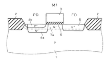
図1は、本実施の形態に係る半導体装置を示す断面図である。図1に示すように、本実施の形態に係る半導体装置は、埋め込みチャネル層7aが設けられている点以外は、図10および図11に示した半導体装置と同様の構成を有している。すなわち、本実施の形態に係る半導体装置はP型半導体基板1を備え、P型半導体基板1の表面には、LOCOS法により形成された素子分離絶縁層2が形成されている。さらに、P型半導体基板1の表面には、フォトダイオードPDと転送スイッチM1とリセットスイッチM2(図1では図示せず)とが並んで配置されている。
【0025】
フォトダイオードPDは、P型半導体基板1とN型不純物領域(N型活性領域)4aとのPN接合により構成されている。そして、N型不純物領域4aの上部(P型半導体基板1の表面近傍)にはP型不純物領域(P型活性領域)4bが形成されている。このP型不純物領域4bは、P型半導体基板1とN型不純物領域4aとのPN接合の空乏層が到達しないような深さに形成されている。
【0026】
転送スイッチM1は、N型ソース領域4a、N型ドレイン領域(N型活性領域、FD領域)5、およびゲート電極層3を有している。N型ソース領域4aとN型ドレイン領域5とは、所定の距離だけ離隔してP型半導体基板1内の表面に形成されている。ゲート電極層3は、P型半導体基板1内のN型ソース領域4aとN型ドレイン領域5とに挟まれる部分の表面上にゲート絶縁層6を介して形成されている。なお、フォトダイオードPDのN型不純物領域4aと転送スイッチM1のN型ソース領域4aとは同一の領域であり、各素子の観点から別個に呼称しているにすぎない。
【0027】
そして、本実施の形態に係る半導体装置では、ゲート電極層3下のP型半導体基板1内チャネル領域、N型ソース領域4aおよびN型ドレイン領域5にわたって、N型ソース領域4aおよびN型ドレイン領域5よりも不純物濃度の低いN型埋め込みチャネル層7aが形成されている。
【0028】
図11に示した半導体装置の構造に加えて、N型埋め込みチャネル層7aをさらに形成した理由は以下のとおりである。
【0029】
図11に示した半導体装置の場合、転送スイッチM1たるMOSトランジスタのチャネルが形成されるのは、P型半導体基板102内の表面部分である。しかし、先述のようにP型半導体基板102内の表面部分には、種々の欠陥が生じやすく、リーク電流を発生させやすい。そこで、チャネルをP型半導体基板102の表面よりも深い部分に形成させることで、それら欠陥の影響を排除することが考えられる。
【0030】
N型埋め込みチャネル層7aをP型半導体基板1内に設けておけば、欠陥の存在するP型半導体基板1の表面付近はポテンシャルが高いが、N型埋め込みチャネル層7aとP型半導体基板1とで構成されるPN接合面付近はポテンシャルが極小となる。よって、転送スイッチM1を動作させたときには、このPN接合面付近にN型ソース領域4aとN型ドレイン領域5とを導通させるチャネルが形成され、リーク電流を発生させることなくN型ソース領域4aに蓄積された電荷をN型ドレイン領域5に伝達することが可能となる。
【0031】
ここで、各領域の不純物種とその濃度の一例を挙げると、P型半導体基板1には、例えばボロンが1×10¹⁵〜1×10¹⁶atoms/cm3程度、N型ソース領域4aおよびN型ドレイン領域5には、例えばリンや砒素が1×1020〜1×1021atoms/cm3程度、P型不純物領域4bには、例えばボロンが1×1017〜1×1018atoms/cm3程度、N型埋め込みチャネル層7aには、例えばリンや砒素が1×1016〜1×1017atoms/cm3程度、それぞれ注入されればよい。
【0032】
なお、上記のような不純物濃度にすることで、N型埋め込みチャネル層7aを設けた場合であっても、転送スイッチM1をエンハンスメント型(ノーマリーオフ型)に保つことができる。
【0033】
また、図1ではN型埋め込みチャネル層7aが、N型ソース領域4aおよびN型ドレイン領域5にまで延在して形成されている。このような構造は、例えばゲート絶縁層6の形成に先立って、素子分離絶縁層2形成済みのP型半導体基板1の表面にリンや砒素等のN型不純物をイオン注入することにより得られる。
【0034】
しかし、N型埋め込みチャネル層7aは、N型ソース領域4aに蓄積された電荷をN型ドレイン領域5に転送するチャネルの機能を有しておればよいので、N型埋め込みチャネル層7aがN型ソース領域4aおよびN型ドレイン領域5にまで延在していることは必ずしも必須ではない。すなわち、N型埋め込みチャネル層7aは、N型ソース領域4aおよびN型ドレイン領域5に接するようにさえ形成されておればよい。
【0035】
本実施の形態によれば、N型ソース領域4aおよびN型ドレイン領域5の両方に接するN型埋め込みチャネル層7aを備える。よって、フォトダイオードPDで発生した電荷を伝達するためのチャネルが、N型埋め込みチャネル層7aとP型半導体基板1との界面付近に形成できる。すなわち、欠陥が生じやすいP型半導体基板1の表面を避けてチャネル形成が行え、リーク電流のより発生しにくい、固体撮像素子を備えた半導体装置を実現できる。
【0036】
<実施の形態2>
本実施の形態は、実施の形態1に係る半導体装置の変形例であり、N型埋め込みチャネル層7aに代わって、ゲート電極層3下における埋め込み層が浅い構造のN型埋め込みチャネル層を備える半導体装置である。
【0037】
図2は、本実施の形態に係る半導体装置を示す断面図である。なお、図2では実施の形態1に係る半導体装置と同様の機能を有する要素については同一符号を付している。図2に示すように、本実施の形態においては、N型埋め込みチャネル層7aに代わって、ゲート電極層3下における埋め込み層7b1が浅い構造のN型埋め込みチャネル層7bが形成されている。その他の構成は実施の形態1に係る半導体装置と同様のため、説明を省略する。
【0038】
このような構造は、埋め込みチャネル層の形成をゲート絶縁層6の形成前ではなく、ゲート絶縁層6およびゲート電極層3の形成後に行うことで得られる。すなわち、素子分離絶縁層2、ゲート絶縁層6およびゲート電極層3形成済みのP型半導体基板1の表面にリンや砒素等のN型不純物をイオン注入することによってN型埋め込みチャネル層7bを形成することができる。
【0039】
このように、プロセス上、埋め込みチャネル層の形成がゲート絶縁層6およびゲート電極層3の形成に前後したとしても、結果的に得られる半導体装置の構造は、ゲート電極層3下における埋め込み層の深浅が異なるだけであるので、本実施の形態に係る半導体装置も実施の形態1に係る半導体装置と同様の効果がある。
【0040】
<実施の形態3>
本実施の形態も、実施の形態1に係る半導体装置の変形例であり、P型不純物領域4bの深さよりもN型埋め込みチャネル層7aの深さを大きくしておくことによって、P型不純物領域4bの端部とN型不純物領域4aの端部とを意図的にずらして形成する必要をなくした半導体装置を実現するものである。
【0041】
図11に示した半導体装置の場合、N型不純物領域104に蓄積された電荷をチャネルを介してN型ドレイン領域106aに転送するためには、ゲート電極層108aのエッジ近傍でN型不純物領域104が、その端部がP型不純物領域105の端部よりもチャネル側に突出したゲートオーバーラップ部分104aを有している必要があった。
【0042】
仮に、N型不純物領域104がゲートオーバーラップ部分104aを有さずに、例えばN型不純物領域104の端部とP型不純物領域105の端部とが同じ位置にあった場合を考えると、ゲート電極層108a下に形成されるチャネルにN型不純物領域104が導通しないことがあり得る。チャネルとN型不純物領域104との間にP型不純物領域105が介在することになるからである。
【0043】
その場合、転送スイッチM1としての機能が阻害されてしまうので、ゲートオーバーラップ部分104aをN型不純物領域104に設けることで、チャネルとN型不純物領域104との間のパスを確保しているのである。
【0044】
しかし、ゲートオーバーラップ部分104aを設けるためには、N型不純物領域104およびP型不純物領域105形成時に不純物注入量や注入角度等を細かく制御する必要があり、製造に困難が伴っていた。
【0045】
また、ゲートオーバーラップ部分104aを設けることができたとしても、P型半導体基板1の表面の欠陥の状態に応じてリーク電流が流れやすかったため、製品間で固体撮像素子としての特性に変動が生じやすかった。
【0046】
そこで、本実施の形態においては、P型不純物領域4bの深さよりもN型埋め込みチャネル層7aの深さを大きくしておくことによって、N型ソース領域4aとチャネルとの安定的なパスを確保する。
【0047】
図3は本実施の形態に係る半導体装置を示す断面図である。なお、図3でも実施の形態1に係る半導体装置と同様の機能を有する要素については同一符号を付している。この半導体装置においては、P型不純物領域4bよりもN型埋め込みチャネル層7aの方が深くなるよう形成されている。また、P型不純物領域4bの端部4b1とN型不純物領域4aの端部4a1とが一致している。その他の構成は実施の形態1に係る半導体装置と同様のため、説明を省略する。
【0048】
このように、N型埋め込みチャネル層7aの方がP型不純物領域4bよりも深く形成されておれば、N型ドレイン領域5側においてP型不純物領域4bの端部4b1がN型不純物領域4aの端部4a1に重なっていたとしても、N型不純物領域4aからN型埋め込みチャネル層7aへと電荷が流れ得る。このため、N型ドレイン領域5側においてP型不純物領域4bの端部4b1とN型不純物領域4aの端部4a1とを意図的にずらして形成する必要はなく、製造が容易な半導体装置が得られる。
【0049】
また、リーク電流が流れやすいP型半導体基板1の表面にN型不純物領域4aからチャネルへのパスを設けるのではないため、N型不純物領域4aからN型埋め込みチャネル層7aへと電荷を安定供給できる。よって、製品間で特性変動の少ない固体撮像素子を備えた半導体装置を実現できる。
【0050】
なお、図1の実施の形態1に係る半導体装置においても、P型不純物領域4bよりもN型埋め込みチャネル層7aの方が深くなるよう形成されていたので、実施の形態1に係る半導体装置も、本実施の形態に係る半導体装置と同様の効果を有している。
【0051】
<実施の形態4>
本実施の形態も、実施の形態1に係る半導体装置の変形例であり、N型ドレイン領域5を設けず、その代わりに、N型ドレイン領域5の領域にまで延在したN型埋め込みチャネル層7aをドレイン領域に利用する半導体装置である。
【0052】
図4は本実施の形態に係る半導体装置を示す断面図である。なお、図4でも実施の形態1に係る半導体装置と同様の機能を有する要素については同一符号を付している。この半導体装置においては、N型ドレイン領域5が省略されている。その他の構成は実施の形態1に係る半導体装置と同様のため、説明を省略する。
【0053】
このように、不純物濃度の高いN型ドレイン領域5を設けないようにすれば、N型ドレイン領域5の形成に伴う不純物注入を行わないで済み、P型半導体基板1の表面に欠陥が生じにくい。よって、リーク電流がより発生しにくくなる。
【0054】
<実施の形態5>
本実施の形態も、実施の形態1に係る半導体装置の変形例であり、N型ドレイン領域5の外縁を、素子分離絶縁層2のエッジから所定の距離だけ離して形成するようにした半導体装置である。
【0055】
図5は本実施の形態に係る半導体装置を示す上面図であり、図6は図5における切断線VI−VIにおける断面図である。なお、図5および図6でも実施の形態1に係る半導体装置と同様の機能を有する要素については同一符号を付している。
【0056】
図5および図6に示すように、本実施の形態においては、素子分離絶縁層2のエッジから所定の距離だけその外縁を離して形成したN型ドレイン領域5aが設けられている。その他の構成は実施の形態1に係る半導体装置と同様のため、説明を省略する。
【0057】
このように、N型ドレイン領域5aの外縁に沿ったエッジを有する素子分離絶縁層2を設けたときに、N型ドレイン領域5aの外縁を、その周囲を取り囲む素子分離絶縁層2のエッジから所定の距離だけ離すことによって、欠陥の生じやすい素子分離絶縁層2のエッジ付近にN型ドレイン領域5aを設けずに済む。よって、リーク電流がより発生しにくくなる。
【0058】
なお、このような構造は、例えばN型ドレイン領域5aをイオン注入により形成する際に、素子分離絶縁層2のエッジよりもより内側にフォトレジストの開口部を形成することで容易に得られる。
【0059】
<実施の形態6>
本実施の形態も実施の形態1に係る半導体装置の変形例であり、P型半導体基板1の表面からのN型埋め込みチャネル層の深さを、少なくともN型不純物領域4aの深さに達するようにした半導体装置である。
【0060】
図7は、本実施の形態に係る半導体装置を示す断面図である。なお、図7でも実施の形態1に係る半導体装置と同様の機能を有する要素については同一符号を付している。
【0061】
図7に示すように、本実施の形態においては、N型埋め込みチャネル層7aをP型半導体基板1の表面からの深さがより大きいN型埋め込みチャネル層7cとして形成している。このN型埋め込みチャネル層7cの深さは、少なくともN型不純物領域4aの深さに達するよう形成されている。その他の構成は実施の形態1に係る半導体装置と同様のため、説明を省略する。
【0062】
このように、N型埋め込みチャネル層7cが少なくともN型不純物領域4aの深さに達しておれば、N型埋め込みチャネル層7cがN型不純物領域4aと一体となって、N型不純物領域4aの不純物濃度、およびN型不純物領域4aのP型半導体基板1との界面の表面積を増加させて、P型半導体基板1とN型不純物領域4aとの間の接合容量を増加させることができる。その結果、フォトダイオードPDで発生する電荷の蓄積量を増やすことができ、信号強度を増加させて画素の特性を向上させることができる。
【0063】
なお、N型埋め込みチャネル層7cを深くする目的は、P型半導体基板1とN型不純物領域4aとの間の接合容量を増加させることにあるので、少なくともN型埋め込みチャネル層7cがN型不純物領域4aにまで延在し、N型不純物領域4aとその近傍においてN型埋め込みチャネル層7cがより深く形成されていることが必要となる。
【0064】
すなわち逆に言えば、N型ドレイン領域5側においてはN型埋め込みチャネル層7cがより深く形成されている必要はない。このことは、次の実施の形態において述べる。
【0065】
<実施の形態7>
本実施の形態は実施の形態6に係る半導体装置の変形例であり、P型半導体基板1の表面からのN型埋め込みチャネル層の深さを、N型ドレイン領域5とその近傍においては、N型不純物領域4a側での深さよりも小さくした半導体装置である。
【0066】
図8は、本実施の形態に係る半導体装置を示す断面図である。なお、図8でも実施の形態6に係る半導体装置と同様の機能を有する要素については同一符号を付している。
【0067】
図8に示すように、本実施の形態においては、N型埋め込みチャネル層7cに代わって、チャネル部分で段差7d1を有するN型埋め込みチャネル層7dが形成されている。このN型埋め込みチャネル層7dのN型不純物領域5およびその近傍での深さは、N型不純物領域4aおよびその近傍でのN型埋め込みチャネル層7dの深さよりも小さくなるよう形成されている。その他の構成は実施の形態6に係る半導体装置と同様のため、説明を省略する。
【0068】
このように、N型ドレイン領域5とその近傍においては、N型埋め込みチャネル層7dの深さをN型不純物領域4a側での深さよりも小さくしておけば、N型埋め込みチャネル層7dと一体化したN型不純物領域4aとP型半導体基板1との界面の表面積より、N型埋め込みチャネル層7dと一体化したN型ドレイン領域5とP型半導体基板1との界面の表面積が大きくなることはなく、N型ドレイン領域5とP型半導体基板1との接合容量をN型不純物領域4aとP型半導体基板1との接合容量よりも小さくすることができる。
【0069】
N型ドレイン領域5とP型半導体基板1との接合容量が小さければ、Q=CV(ただし、Q:フォトダイオードPDで発生した電荷量、C:N型ドレイン領域5とP型半導体基板1との接合容量、V:N型ドレイン領域5にて出力される電圧信号)の関係より、同じ電荷量であっても電圧信号が大きく出力されることになる。これにより、N型ドレイン領域5から出力される電圧信号を強化することができる。
【0070】
なお、上記のようなチャネル部分で段差7d1を有するN型埋め込みチャネル層7dは、その形成を行なう際に例えば、段差7d1よりもN型ドレイン領域5側の領域を形成するフォトマスクと、段差7d1よりもN型不純物領域4a側の領域を形成するフォトマスクとをそれぞれ用意して、イオン注入の深さを変えることにより形成することができる。
【0071】
【発明の効果】
請求項1に記載の発明によれば、第1および第2活性領域の両方に接する埋め込みチャネル層を備える。よって、フォトダイオードで発生した電荷を伝達するためのチャネルが、埋め込みチャネル層と半導体基板との界面付近に形成できる。すなわち、欠陥が生じやすい半導体基板表面を避けてチャネル形成が行え、リーク電流のより発生しにくい、固体撮像素子を備えた半導体装置を実現できる。また、本発明によれば、埋め込みチャネル層は、第1活性領域の設けられた部分にまで延在するよう第1活性領域に重ねて設けられ、第1活性領域およびその近傍において、埋め込みチャネル層は少なくとも第1活性領域の深さに達する。よって、埋め込みチャネル層が第1活性領域と一体となって、第1活性領域の不純物濃度および半導体基板との界面の表面積を増加させて、半導体基板と第1活性領域との間の接合容量を増加させることができる。その結果、フォトダイオードで発生する電荷の蓄積量を増やすことができ、信号強度を増加させて画素の特性を向上させることができる。
【0072】
請求項2に記載の発明によれば、埋め込みチャネル層の方が第3活性領域よりも深い。よって、第2活性領域側において第3活性領域の端部が第1活性領域の端部に重なっていたとしても、第1活性領域から埋め込みチャネル層へと電荷が流れ得る。このため、第2活性領域側において第3活性領域の端部と第1活性領域の端部とを意図的にずらして形成する必要はなく、製造が容易な半導体装置が得られる。また、リーク電流が流れやすい半導体基板の表面に第1活性領域からチャネルへのパスを設けるのではないため、第1活性領域から埋め込みチャネル層へと電荷を安定供給できる。その結果、製品間で特性変動の少ない固体撮像素子を備えた半導体装置を実現できる。
【0073】
請求項3に記載の発明によれば、第2活性領域を設けず、その代わりに、第2活性領域の設けられるべき領域にまで埋め込みチャネル層を延在させている。不純物濃度の高い第2活性領域を設けないことから、第2活性領域の形成に伴う不純物注入を行わないで済み、半導体基板表面に欠陥が生じにくい。よって、リーク電流がより発生しにくくなる。
【0074】
請求項4に記載の発明によれば、第2活性領域は、その外縁が素子分離絶縁層のエッジから所定の距離だけ離れて半導体基板内に設けられる。よって、欠陥の生じやすい素子分離絶縁層のエッジ付近に第2活性領域が設けられることがなく、リーク電流がより発生しにくくなる。
【0076】
請求項5に記載の発明によれば、第2活性領域およびその近傍においては、埋め込みチャネル層の深さは、第1活性領域およびその近傍における埋め込みチャネル層の深さよりも小さい。よって、埋め込みチャネル層と一体化した第1活性領域と半導体基板との界面の表面積より、埋め込みチャネル層と一体化した第2活性領域と半導体基板との界面の表面積が大きくなることはなく、第2活性領域と半導体基板との接合容量を第1活性領域と半導体基板との接合容量よりも小さくすることができる。これにより、第2活性領域から出力される電圧信号を強化することができる。
【図面の簡単な説明】
【図1】 実施の形態1に係る半導体装置を示す断面図である。
【図2】 実施の形態2に係る半導体装置を示す断面図である。
【図3】 実施の形態3に係る半導体装置を示す断面図である。
【図4】 実施の形態4に係る半導体装置を示す断面図である。
【図5】 実施の形態5に係る半導体装置を示す上面図である。
【図6】 実施の形態5に係る半導体装置を示す断面図である。
【図7】 実施の形態6に係る半導体装置を示す断面図である。
【図8】 実施の形態7に係る半導体装置を示す断面図である。
【図9】 CMOS型のイメージセンサを備えた半導体装置の回路構成を示す図である。
【図10】 従来の半導体装置を示す上面図である。
【図11】 従来の半導体装置を示す断面図である。
【符号の説明】
1 P型半導体基板、2 素子分離絶縁層、3 ゲート電極層、4a N型不純物領域(N型ソース領域)、4b P型不純物領域、5,5a N型ドレイン領域、6 ゲート絶縁層、7a〜7d N型埋め込みチャネル層。[0001]
BACKGROUND OF THE INVENTION
The present invention relates to a semiconductor device provided with a solid-state image sensor.
[0002]
[Prior art]
In recent years, one using an amplification type sensor has been proposed as one of solid-state imaging devices. This element has a feature of amplifying a light signal detected by the photoelectric conversion storage unit in the vicinity of the photoelectric conversion storage unit.
[0003]
FIG. 9 is a diagram illustrating a circuit configuration of a semiconductor device including a complementary metal oxide semiconductor (CMOS) type image sensor as a solid-state imaging device. As shown in FIG. 9, unit pixels or unit cells C are arranged in a matrix, and each cell C is connected to a vertical shift register VS and a horizontal shift register HS.
[0004]
Each unit cell C includes a photodiode PD, a transfer switch M1, a reset switch M2, an amplifier M3, and a selection switch M4. The photodiode PD has a role as a photoelectric conversion accumulation unit that converts incident light into an electric signal and accumulates the generated charges. The transfer switch M1 has a role of transferring the converted electric signal to the amplifier M3, and its control is performed by a signal from the vertical shift register VS. The reset switch M2 has a role of resetting the signal charge, and the amplifier M3 has a role of amplifying the electric signal.
[0005]
Note that each of the transfer switch M1, the reset switch M2, the amplifier M3, and the selection switch M4 is configured by a MOS transistor.
[0006]
FIG. 10 is a top view showing a specific configuration of the region R in FIG. FIG. 11 is a cross-sectional view taken along section line XI-XI in FIG.
[0007]
As shown in FIGS. 10 and 11, an element
[0008]
The photodiode PD is configured by a PN junction between a P-
[0009]
The transfer switch M1 includes an N-
[0010]
The reset switch M2 has a pair of N-type source /
[0011]
[Problems to be solved by the invention]
In the CMOS image sensor shown in FIGS. 10 and 11, the charge generated in the photodiode PD is transferred to the N-type drain via a channel formed on the surface of the P-
[0012]
In the surface of the P-
[0013]
Therefore, a part of the signal charges generated in the photodiode PD flows through these defects, and a leak current is generated. When the leak current is generated, the amount of charge transferred to the N-
[0014]
The P-
[0015]
However, it cannot be said that the leakage current can be sufficiently suppressed only by providing the P-
[0016]
SUMMARY OF THE INVENTION An object of the present invention is to provide a semiconductor device including a solid-state imaging element that is less likely to generate a leakage current.
[0017]
[Means for Solving the Problems]
The invention according to
[0018]
The invention according to
[0019]
A third aspect of the present invention is the semiconductor device according to the first aspect, wherein the second active region is not provided, and instead, the buried channel layer is extended to a region where the second active region is to be provided. This is a semiconductor device in which is extended.
[0020]
The invention according to
[0022]
Claim5The invention described in claim1The buried channel layer is provided so as to overlap the second active region so as to further extend to a portion where the second active region is provided, the second active region and the second active region In the vicinity, the depth of the buried channel layer from the surface of the semiconductor substrate is a semiconductor device smaller than the depth of the buried channel layer in the first active region and the vicinity thereof.
[0023]
DETAILED DESCRIPTION OF THE INVENTION
<
In this embodiment, by providing a buried channel layer, a channel is formed avoiding the surface of a semiconductor substrate where defects are likely to occur, and a semiconductor device including a solid-state imaging element that is less likely to generate a leakage current is realized. is there.
[0024]
FIG. 1 is a cross-sectional view showing a semiconductor device according to the present embodiment. As shown in FIG. 1, the semiconductor device according to the present embodiment has the same configuration as the semiconductor device shown in FIGS. 10 and 11 except that a buried
[0025]
The photodiode PD is configured by a PN junction between the P-
[0026]
The transfer switch M1 has an N-
[0027]
In the semiconductor device according to the present embodiment, the N-
[0028]
The reason why the N-type buried
[0029]
In the semiconductor device shown in FIG. 11, the channel of the MOS transistor serving as the transfer switch M <b> 1 is formed on the surface portion in the P-
[0030]
If the N-type buried
[0031]
Here, as an example of the impurity species and their concentrations in each region, the P-
[0032]
By setting the impurity concentration as described above, the transfer switch M1 can be kept in the enhancement type (normally off type) even when the N-type buried
[0033]
In FIG. 1, the N-type buried
[0034]
However, the N-type buried
[0035]
According to the present embodiment, the N-type buried
[0036]
<
The present embodiment is a modification of the semiconductor device according to the first embodiment, and a semiconductor including an N-type buried channel layer having a shallow buried layer under the
[0037]
FIG. 2 is a cross-sectional view showing the semiconductor device according to the present embodiment. In FIG. 2, elements having the same functions as those of the semiconductor device according to the first embodiment are denoted by the same reference numerals. As shown in FIG. 2, in this embodiment, an N-type buried
[0038]
Such a structure can be obtained by forming the buried channel layer not after the formation of the gate insulating layer 6 but after the formation of the gate insulating layer 6 and the
[0039]
As described above, even if the formation of the buried channel layer is before or after the formation of the gate insulating layer 6 and the
[0040]
<
The present embodiment is also a modification of the semiconductor device according to the first embodiment, and by making the depth of the N-type buried
[0041]
In the case of the semiconductor device shown in FIG. 11, in order to transfer the charge accumulated in the N-
[0042]
If the N-
[0043]
In that case, since the function as the transfer switch M1 is hindered, the path between the channel and the N-
[0044]
However, in order to provide the
[0045]
Even if the
[0046]
Therefore, in the present embodiment, a stable path between the N-
[0047]
FIG. 3 is a cross-sectional view showing the semiconductor device according to the present embodiment. In FIG. 3, elements having the same functions as those of the semiconductor device according to the first embodiment are denoted by the same reference numerals. In this semiconductor device, the N-type buried
[0048]
Thus, if the N-type buried
[0049]
In addition, since a path from the N-
[0050]
In the semiconductor device according to the first embodiment shown in FIG. 1, the N-type buried
[0051]
<
The present embodiment is also a modification of the semiconductor device according to the first embodiment, in which the N-
[0052]
FIG. 4 is a cross-sectional view showing the semiconductor device according to the present embodiment. In FIG. 4, elements having the same functions as those of the semiconductor device according to the first embodiment are denoted by the same reference numerals. In this semiconductor device, the N-
[0053]
As described above, if the N-
[0054]
<
This embodiment is also a modification of the semiconductor device according to the first embodiment, in which the outer edge of the N-
[0055]
FIG. 5 is a top view showing the semiconductor device according to the present embodiment, and FIG. 6 is a cross-sectional view taken along section line VI-VI in FIG. 5 and 6, elements having the same functions as those of the semiconductor device according to the first embodiment are denoted by the same reference numerals.
[0056]
As shown in FIGS. 5 and 6, in the present embodiment, an N-
[0057]
As described above, when the element
[0058]
Such a structure can be easily obtained by forming a photoresist opening inside the edge of the element
[0059]
<Embodiment 6>
This embodiment is also a modification of the semiconductor device according to the first embodiment, and the depth of the N-type buried channel layer from the surface of the P-
[0060]
FIG. 7 is a cross-sectional view showing the semiconductor device according to the present embodiment. In FIG. 7, elements having the same functions as those of the semiconductor device according to the first embodiment are denoted by the same reference numerals.
[0061]
As shown in FIG. 7, in this embodiment, the N-type buried
[0062]
As described above, if the N-type buried channel layer 7c reaches at least the depth of the N-
[0063]
The purpose of deepening the N-type buried channel layer 7c is to increase the junction capacitance between the P-
[0064]
In other words, the N-type buried channel layer 7c does not need to be formed deeper on the N-
[0065]
<
The present embodiment is a modification of the semiconductor device according to the sixth embodiment. The depth of the N-type buried channel layer from the surface of the P-
[0066]
FIG. 8 is a cross-sectional view showing the semiconductor device according to the present embodiment. In FIG. 8, elements having the same functions as those of the semiconductor device according to the sixth embodiment are denoted by the same reference numerals.
[0067]
As shown in FIG. 8, in the present embodiment, instead of the N-type buried channel layer 7c, an N-type buried
[0068]
As described above, in the N-
[0069]
If the junction capacitance between the N-
[0070]
The N-type buried
[0071]
【The invention's effect】
According to the first aspect of the present invention, the buried channel layer is provided in contact with both the first and second active regions. Therefore, a channel for transmitting charges generated in the photodiode can be formed in the vicinity of the interface between the buried channel layer and the semiconductor substrate. That is, it is possible to realize a semiconductor device including a solid-state imaging device that can perform channel formation while avoiding the surface of a semiconductor substrate where defects are likely to occur, and is less likely to generate a leakage current.Further, according to the present invention, the buried channel layer is provided so as to overlap the first active region so as to extend to a portion where the first active region is provided, and in the first active region and the vicinity thereof, the buried channel layer is provided. Reaches at least the depth of the first active region. Therefore, the buried channel layer is integrated with the first active region to increase the impurity concentration of the first active region and the surface area of the interface with the semiconductor substrate, thereby increasing the junction capacitance between the semiconductor substrate and the first active region. Can be increased. As a result, the amount of charge generated in the photodiode can be increased, and the signal intensity can be increased to improve the characteristics of the pixel.
[0072]
According to the second aspect of the present invention, the buried channel layer is deeper than the third active region. Therefore, even if the end of the third active region overlaps the end of the first active region on the second active region side, charge can flow from the first active region to the buried channel layer. Therefore, it is not necessary to intentionally shift the end of the third active region and the end of the first active region on the second active region side, and a semiconductor device that is easy to manufacture can be obtained. In addition, since a path from the first active region to the channel is not provided on the surface of the semiconductor substrate where leakage current tends to flow, charges can be stably supplied from the first active region to the buried channel layer. As a result, it is possible to realize a semiconductor device including a solid-state imaging element with little characteristic variation between products.
[0073]
According to the third aspect of the present invention, the second active region is not provided, and instead, the buried channel layer is extended to the region where the second active region is to be provided. Since the second active region having a high impurity concentration is not provided, it is not necessary to perform impurity implantation accompanying the formation of the second active region, and defects on the surface of the semiconductor substrate are hardly generated. Therefore, the leak current is less likely to occur.
[0074]
According to the invention described in
[0076]
Claim5According to the invention described in (1), the depth of the buried channel layer in the second active region and the vicinity thereof is smaller than the depth of the buried channel layer in the first active region and the vicinity thereof. Therefore, the surface area of the interface between the second active region integrated with the buried channel layer and the semiconductor substrate does not become larger than the surface area of the interface between the first active region integrated with the buried channel layer and the semiconductor substrate. The junction capacitance between the two active regions and the semiconductor substrate can be made smaller than the junction capacitance between the first active region and the semiconductor substrate. Thereby, the voltage signal output from the second active region can be enhanced.
[Brief description of the drawings]
FIG. 1 is a cross-sectional view showing a semiconductor device according to a first embodiment.
FIG. 2 is a cross-sectional view showing a semiconductor device according to a second embodiment.
FIG. 3 is a cross-sectional view showing a semiconductor device according to a third embodiment.
4 is a cross-sectional view showing a semiconductor device according to a fourth embodiment. FIG.
FIG. 5 is a top view showing a semiconductor device according to a fifth embodiment.
FIG. 6 is a cross-sectional view showing a semiconductor device according to a fifth embodiment.
FIG. 7 is a sectional view showing a semiconductor device according to a sixth embodiment.
FIG. 8 is a cross-sectional view showing a semiconductor device according to a seventh embodiment.
FIG. 9 is a diagram illustrating a circuit configuration of a semiconductor device including a CMOS type image sensor.
FIG. 10 is a top view showing a conventional semiconductor device.
FIG. 11 is a cross-sectional view showing a conventional semiconductor device.
[Explanation of symbols]
1 P-type semiconductor substrate, 2 element isolation insulating layer, 3 gate electrode layer, 4a N-type impurity region (N-type source region), 4b P-type impurity region, 5, 5a N-type drain region, 6 gate insulating layer, 7a to 7d N-type buried channel layer.
Claims (5)
前記半導体基板内の表面に設けられた、前記第1導電型とは異なる第2導電型の第1活性領域と、
前記半導体基板内の表面に前記第1活性領域とは離隔して設けられた、前記第2導電型の第2活性領域と、
前記半導体基板内の前記第1および第2活性領域に挟まれた部分の表面上に設けられた制御電極と、
前記制御電極下の前記半導体基板内に設けられた、前記第1および第2活性領域の両方に接する前記第2導電型の埋め込みチャネル層と
を備え、
前記半導体基板と前記第1活性領域とは、固体撮像素子の一部たるフォトダイオードを構成し、
前記制御電極と前記第1および第2活性領域とは、固体撮像素子の一部たるトランジスタを構成し、
前記埋め込みチャネル層の不純物濃度は、前記第1および第2活性領域の不純物濃度よりも低く、
前記埋め込みチャネル層は、前記第1活性領域の設けられた部分にまで延在するよう前記第1活性領域に重ねて設けられ、
前記第1活性領域およびその近傍において、前記半導体基板の表面からの前記埋め込みチャネル層の深さは少なくとも、前記半導体基板の表面からの前記第1活性領域の深さに達する
半導体装置。A first conductivity type semiconductor substrate;
A first active region of a second conductivity type different from the first conductivity type provided on a surface in the semiconductor substrate;
A second active region of the second conductivity type provided on the surface in the semiconductor substrate and spaced apart from the first active region;
A control electrode provided on a surface of a portion sandwiched between the first and second active regions in the semiconductor substrate;
A buried channel layer of the second conductivity type provided in the semiconductor substrate under the control electrode and in contact with both the first and second active regions;
The semiconductor substrate and the first active region constitute a photodiode that is a part of a solid-state imaging device,
The control electrode and the first and second active regions constitute a transistor that is a part of a solid-state imaging device,
The impurity concentration of the buried channel layer, rather lower than the impurity concentration of said first and second active regions,
The buried channel layer is provided to overlap the first active region so as to extend to a portion where the first active region is provided;
In the first active region and the vicinity thereof, the depth of the buried channel layer from the surface of the semiconductor substrate reaches at least the depth of the first active region from the surface of the semiconductor substrate. .
前記第1活性領域内の表面に設けられた、前記第1導電型の第3活性領域をさらに備え、
前記半導体基板の表面からの前記埋め込みチャネル層の深さは、前記半導体基板の表面からの前記第3活性領域の深さよりも大きい
半導体装置。The semiconductor device according to claim 1,
A third active region of the first conductivity type provided on a surface in the first active region;
The depth of the buried channel layer from the surface of the semiconductor substrate is greater than the depth of the third active region from the surface of the semiconductor substrate.
前記第2活性領域を設けず、その代わりに、前記第2活性領域の設けられるべき領域にまで前記埋め込みチャネル層を延在させた
半導体装置。The semiconductor device according to claim 1,
A semiconductor device in which the second active region is not provided, and instead, the buried channel layer is extended to a region where the second active region is to be provided.
前記半導体基板表面に設けられた、前記第2活性領域の外縁に沿ったエッジを有する素子分離絶縁層
をさらに備え、
前記第2活性領域は、その前記外縁が前記素子分離絶縁層の前記エッジから所定の距離だけ離れて前記半導体基板内に設けられた
半導体装置。The semiconductor device according to claim 1,
An element isolation insulating layer having an edge along the outer edge of the second active region provided on the surface of the semiconductor substrate;
The second active region is a semiconductor device in which the outer edge is provided in the semiconductor substrate at a predetermined distance from the edge of the element isolation insulating layer.
前記埋め込みチャネル層は、前記第2活性領域の設けられた部分にまでさらに延在するよう前記第2活性領域に重ねて設けられ、
前記第2活性領域およびその近傍においては、前記半導体基板の表面からの前記埋め込みチャネル層の深さは、前記第1活性領域およびその近傍における前記埋め込みチャネル層の深さよりも小さい
半導体装置。The semiconductor device according to claim 1,
The buried channel layer is provided to overlap the second active region so as to further extend to a portion where the second active region is provided;
In the second active region and the vicinity thereof, the depth of the buried channel layer from the surface of the semiconductor substrate is smaller than the depth of the buried channel layer in the first active region and the vicinity thereof. apparatus.
Priority Applications (2)
| Application Number | Priority Date | Filing Date | Title |
|---|---|---|---|
| JP2001359160A JP3779199B2 (en) | 2001-11-26 | 2001-11-26 | Semiconductor device |
| US10/121,699 US6566678B1 (en) | 2001-11-26 | 2002-04-15 | Semiconductor device having a solid-state image sensor |
Applications Claiming Priority (1)
| Application Number | Priority Date | Filing Date | Title |
|---|---|---|---|
| JP2001359160A JP3779199B2 (en) | 2001-11-26 | 2001-11-26 | Semiconductor device |
Publications (2)
| Publication Number | Publication Date |
|---|---|
| JP2003158255A JP2003158255A (en) | 2003-05-30 |
| JP3779199B2 true JP3779199B2 (en) | 2006-05-24 |
Family
ID=19170217
Family Applications (1)
| Application Number | Title | Priority Date | Filing Date |
|---|---|---|---|
| JP2001359160A Expired - Fee Related JP3779199B2 (en) | 2001-11-26 | 2001-11-26 | Semiconductor device |
Country Status (2)
| Country | Link |
|---|---|
| US (1) | US6566678B1 (en) |
| JP (1) | JP3779199B2 (en) |
Families Citing this family (15)
| Publication number | Priority date | Publication date | Assignee | Title |
|---|---|---|---|---|
| JP2003031787A (en) * | 2001-07-17 | 2003-01-31 | Canon Inc | Solid state image sensor and its driving method |
| KR100462164B1 (en) * | 2002-01-11 | 2004-12-17 | 매그나칩 반도체 유한회사 | Cmos image sensor with enhanced fill factor |
| JP4219755B2 (en) * | 2003-07-16 | 2009-02-04 | ローム株式会社 | Image sensor manufacturing method and image sensor |
| US7420233B2 (en) * | 2003-10-22 | 2008-09-02 | Micron Technology, Inc. | Photodiode for improved transfer gate leakage |
| JP4513497B2 (en) * | 2004-10-19 | 2010-07-28 | ソニー株式会社 | Solid-state imaging device |
| JP5361110B2 (en) * | 2004-10-20 | 2013-12-04 | 三星電子株式会社 | Solid-state image sensor element having non-planar transistor and manufacturing method thereof |
| KR100660275B1 (en) * | 2004-12-29 | 2006-12-20 | 동부일렉트로닉스 주식회사 | Transfer Transistor of CMOS Image Sensor and Manufacturing Method Thereof |
| KR100760142B1 (en) * | 2005-07-27 | 2007-09-18 | 매그나칩 반도체 유한회사 | Stacked pixel for high resolution cmos image sensors |
| JP2007184368A (en) * | 2006-01-05 | 2007-07-19 | Toshiba Corp | Solid-state image sensor |
| JP4857816B2 (en) * | 2006-02-28 | 2012-01-18 | ソニー株式会社 | Solid-state image sensor |
| JP5335271B2 (en) | 2008-04-09 | 2013-11-06 | キヤノン株式会社 | Photoelectric conversion device and imaging system using the same |
| KR101363532B1 (en) * | 2009-10-05 | 2014-02-14 | 고쿠리츠 다이가꾸 호우진 시즈오까 다이가꾸 | Semiconductor element and solid-state imaging device |
| US20110215226A1 (en) * | 2010-03-03 | 2011-09-08 | Dmitri Jerdev | Photosensitive structure with charge amplification |
| FR2986906B1 (en) * | 2012-02-15 | 2015-06-19 | New Imaging Technologies Sas | IMPROVED LOAD TRANSFER ACTIVE PIXEL STRUCTURE |
| CN111370435B (en) * | 2020-03-11 | 2022-11-15 | 深圳市昊岳科技有限公司 | Image sensor and manufacturing method thereof |
Family Cites Families (2)
| Publication number | Priority date | Publication date | Assignee | Title |
|---|---|---|---|---|
| JPS59107568A (en) | 1982-12-13 | 1984-06-21 | Hitachi Ltd | Solid-state image pick-up device |
| JPH0685233A (en) | 1992-09-03 | 1994-03-25 | Matsushita Electron Corp | Manufacture of solid-state image sensing device |
-
2001
- 2001-11-26 JP JP2001359160A patent/JP3779199B2/en not_active Expired - Fee Related
-
2002
- 2002-04-15 US US10/121,699 patent/US6566678B1/en not_active Expired - Lifetime
Also Published As
| Publication number | Publication date |
|---|---|
| US6566678B1 (en) | 2003-05-20 |
| JP2003158255A (en) | 2003-05-30 |
| US20030098454A1 (en) | 2003-05-29 |
Similar Documents
| Publication | Publication Date | Title |
|---|---|---|
| US9887226B2 (en) | Solid-state imaging device | |
| JP4224036B2 (en) | Image sensor with embedded photodiode region and method of manufacturing the same | |
| JP3584196B2 (en) | Light receiving element and photoelectric conversion device having the same | |
| JP3779199B2 (en) | Semiconductor device | |
| JP3403061B2 (en) | Solid-state imaging device | |
| US7397100B2 (en) | Image sensor and method of manufacturing the same | |
| JP4406964B2 (en) | Solid-state imaging device and manufacturing method thereof | |
| WO2014002362A1 (en) | Solid-state image pickup apparatus and method for manufacturing same | |
| JPH11274450A (en) | Solid-state image pick up device | |
| JP2002043557A (en) | Semiconductor device comprising solid-state imaging element and manufacturing method thereof | |
| JP2005347759A (en) | Image sensor for reducing dark current, and manufacturing method therefor | |
| US20090065829A1 (en) | Image Sensor and Method for Manufacturing the Same | |
| JP4449106B2 (en) | MOS type solid-state imaging device and manufacturing method thereof | |
| TWI536553B (en) | Solid-state imaging device and method for manufacturing solid-state imaging device | |
| JP2004014861A (en) | Semiconductor device and method for manufacturing the semiconductor device | |
| JP2009188380A (en) | Image sensor and method for manufacturing the same | |
| JP3621273B2 (en) | Solid-state imaging device and manufacturing method thereof | |
| JP4763242B2 (en) | Solid-state imaging device and manufacturing method thereof | |
| KR101024815B1 (en) | Image Sensor and Method for Manufacturing thereof | |
| US7763909B2 (en) | Image sensor and method for manufacturing the same | |
| KR101135791B1 (en) | Image Sensor and Method for Manufacturing thereof | |
| KR20070073633A (en) | Solid-state image pickup device | |
| JP2006019487A (en) | Amplification type solid-state image pickup device | |
| JP3597663B2 (en) | Solid-state imaging device | |
| JP2007165450A (en) | Solid-state image pickup element |
Legal Events
| Date | Code | Title | Description |
|---|---|---|---|
| A621 | Written request for application examination |
Free format text: JAPANESE INTERMEDIATE CODE: A621 Effective date: 20041122 |
|
| A977 | Report on retrieval |
Free format text: JAPANESE INTERMEDIATE CODE: A971007 Effective date: 20051125 |
|
| A131 | Notification of reasons for refusal |
Free format text: JAPANESE INTERMEDIATE CODE: A131 Effective date: 20051206 |
|
| A521 | Request for written amendment filed |
Free format text: JAPANESE INTERMEDIATE CODE: A523 Effective date: 20060131 |
|
| TRDD | Decision of grant or rejection written | ||
| A01 | Written decision to grant a patent or to grant a registration (utility model) |
Free format text: JAPANESE INTERMEDIATE CODE: A01 Effective date: 20060228 |
|
| A61 | First payment of annual fees (during grant procedure) |
Free format text: JAPANESE INTERMEDIATE CODE: A61 Effective date: 20060301 |
|
| R150 | Certificate of patent or registration of utility model |
Free format text: JAPANESE INTERMEDIATE CODE: R150 |
|
| FPAY | Renewal fee payment (event date is renewal date of database) |
Free format text: PAYMENT UNTIL: 20090310 Year of fee payment: 3 |
|
| FPAY | Renewal fee payment (event date is renewal date of database) |
Free format text: PAYMENT UNTIL: 20100310 Year of fee payment: 4 |
|
| FPAY | Renewal fee payment (event date is renewal date of database) |
Free format text: PAYMENT UNTIL: 20110310 Year of fee payment: 5 |
|
| FPAY | Renewal fee payment (event date is renewal date of database) |
Free format text: PAYMENT UNTIL: 20110310 Year of fee payment: 5 |
|
| S111 | Request for change of ownership or part of ownership |
Free format text: JAPANESE INTERMEDIATE CODE: R313111 |
|
| FPAY | Renewal fee payment (event date is renewal date of database) |
Free format text: PAYMENT UNTIL: 20110310 Year of fee payment: 5 |
|
| R350 | Written notification of registration of transfer |
Free format text: JAPANESE INTERMEDIATE CODE: R350 |
|
| FPAY | Renewal fee payment (event date is renewal date of database) |
Free format text: PAYMENT UNTIL: 20110310 Year of fee payment: 5 |
|
| FPAY | Renewal fee payment (event date is renewal date of database) |
Free format text: PAYMENT UNTIL: 20120310 Year of fee payment: 6 |
|
| FPAY | Renewal fee payment (event date is renewal date of database) |
Free format text: PAYMENT UNTIL: 20130310 Year of fee payment: 7 |
|
| FPAY | Renewal fee payment (event date is renewal date of database) |
Free format text: PAYMENT UNTIL: 20130310 Year of fee payment: 7 |
|
| FPAY | Renewal fee payment (event date is renewal date of database) |
Free format text: PAYMENT UNTIL: 20140310 Year of fee payment: 8 |
|
| S531 | Written request for registration of change of domicile |
Free format text: JAPANESE INTERMEDIATE CODE: R313531 |
|
| R350 | Written notification of registration of transfer |
Free format text: JAPANESE INTERMEDIATE CODE: R350 |
|
| LAPS | Cancellation because of no payment of annual fees |