JP3765314B2 - Mask, mask manufacturing method, electro-optical device manufacturing method, and electronic apparatus - Google Patents
Mask, mask manufacturing method, electro-optical device manufacturing method, and electronic apparatus Download PDFInfo
- Publication number
- JP3765314B2 JP3765314B2 JP2004104311A JP2004104311A JP3765314B2 JP 3765314 B2 JP3765314 B2 JP 3765314B2 JP 2004104311 A JP2004104311 A JP 2004104311A JP 2004104311 A JP2004104311 A JP 2004104311A JP 3765314 B2 JP3765314 B2 JP 3765314B2
- Authority
- JP
- Japan
- Prior art keywords
- mask
- manufacturing
- opening
- roundness
- silicon
- Prior art date
- Legal status (The legal status is an assumption and is not a legal conclusion. Google has not performed a legal analysis and makes no representation as to the accuracy of the status listed.)
- Expired - Fee Related
Links
- 238000004519 manufacturing process Methods 0.000 title claims description 70
- 239000000758 substrate Substances 0.000 claims description 94
- XUIMIQQOPSSXEZ-UHFFFAOYSA-N Silicon Chemical compound [Si] XUIMIQQOPSSXEZ-UHFFFAOYSA-N 0.000 claims description 91
- 229910052710 silicon Inorganic materials 0.000 claims description 91
- 239000010703 silicon Substances 0.000 claims description 91
- 238000005530 etching Methods 0.000 claims description 46
- 239000010408 film Substances 0.000 claims description 38
- 238000000034 method Methods 0.000 claims description 36
- 239000010409 thin film Substances 0.000 claims description 31
- 239000000463 material Substances 0.000 claims description 30
- KRHYYFGTRYWZRS-UHFFFAOYSA-N Fluorane Chemical compound F KRHYYFGTRYWZRS-UHFFFAOYSA-N 0.000 claims description 20
- 239000013078 crystal Substances 0.000 claims description 18
- QTBSBXVTEAMEQO-UHFFFAOYSA-N Acetic acid Chemical compound CC(O)=O QTBSBXVTEAMEQO-UHFFFAOYSA-N 0.000 claims description 16
- 238000000059 patterning Methods 0.000 claims description 13
- 239000000126 substance Substances 0.000 claims description 12
- 239000000470 constituent Substances 0.000 claims description 11
- 238000001312 dry etching Methods 0.000 claims description 9
- 230000008569 process Effects 0.000 claims description 9
- GRYLNZFGIOXLOG-UHFFFAOYSA-N Nitric acid Chemical compound O[N+]([O-])=O GRYLNZFGIOXLOG-UHFFFAOYSA-N 0.000 claims description 8
- 229910017604 nitric acid Inorganic materials 0.000 claims description 8
- 230000000149 penetrating effect Effects 0.000 claims description 3
- ZAMOUSCENKQFHK-UHFFFAOYSA-N Chlorine atom Chemical compound [Cl] ZAMOUSCENKQFHK-UHFFFAOYSA-N 0.000 claims description 2
- 239000000460 chlorine Substances 0.000 claims description 2
- 229910052801 chlorine Inorganic materials 0.000 claims description 2
- 238000007740 vapor deposition Methods 0.000 description 43
- 101100269850 Caenorhabditis elegans mask-1 gene Proteins 0.000 description 24
- 230000015572 biosynthetic process Effects 0.000 description 13
- 239000011521 glass Substances 0.000 description 13
- 238000000151 deposition Methods 0.000 description 11
- 230000008021 deposition Effects 0.000 description 11
- 229910052751 metal Inorganic materials 0.000 description 11
- 239000002184 metal Substances 0.000 description 11
- VYPSYNLAJGMNEJ-UHFFFAOYSA-N Silicium dioxide Chemical compound O=[Si]=O VYPSYNLAJGMNEJ-UHFFFAOYSA-N 0.000 description 10
- 229910052814 silicon oxide Inorganic materials 0.000 description 10
- 230000001154 acute effect Effects 0.000 description 8
- 239000007789 gas Substances 0.000 description 6
- 230000005291 magnetic effect Effects 0.000 description 6
- 238000000206 photolithography Methods 0.000 description 6
- 239000000243 solution Substances 0.000 description 5
- XEEYBQQBJWHFJM-UHFFFAOYSA-N Iron Chemical compound [Fe] XEEYBQQBJWHFJM-UHFFFAOYSA-N 0.000 description 4
- 230000004048 modification Effects 0.000 description 4
- 238000012986 modification Methods 0.000 description 4
- 239000011368 organic material Substances 0.000 description 4
- PXHVJJICTQNCMI-UHFFFAOYSA-N Nickel Chemical compound [Ni] PXHVJJICTQNCMI-UHFFFAOYSA-N 0.000 description 3
- KWYUFKZDYYNOTN-UHFFFAOYSA-M Potassium hydroxide Chemical compound [OH-].[K+] KWYUFKZDYYNOTN-UHFFFAOYSA-M 0.000 description 3
- 239000000956 alloy Substances 0.000 description 3
- 229910045601 alloy Inorganic materials 0.000 description 3
- 238000005229 chemical vapour deposition Methods 0.000 description 3
- 230000010365 information processing Effects 0.000 description 3
- 239000007769 metal material Substances 0.000 description 3
- 238000006748 scratching Methods 0.000 description 3
- 230000002393 scratching effect Effects 0.000 description 3
- 238000004544 sputter deposition Methods 0.000 description 3
- RZVAJINKPMORJF-UHFFFAOYSA-N Acetaminophen Chemical compound CC(=O)NC1=CC=C(O)C=C1 RZVAJINKPMORJF-UHFFFAOYSA-N 0.000 description 2
- KZBUYRJDOAKODT-UHFFFAOYSA-N Chlorine Chemical compound ClCl KZBUYRJDOAKODT-UHFFFAOYSA-N 0.000 description 2
- -1 aluminum quinolinol Chemical compound 0.000 description 2
- 239000007864 aqueous solution Substances 0.000 description 2
- 230000008901 benefit Effects 0.000 description 2
- 230000008859 change Effects 0.000 description 2
- 238000010586 diagram Methods 0.000 description 2
- 238000009826 distribution Methods 0.000 description 2
- 230000008020 evaporation Effects 0.000 description 2
- 238000001704 evaporation Methods 0.000 description 2
- 230000005525 hole transport Effects 0.000 description 2
- 238000007654 immersion Methods 0.000 description 2
- 230000006872 improvement Effects 0.000 description 2
- 229910052742 iron Inorganic materials 0.000 description 2
- 239000011159 matrix material Substances 0.000 description 2
- 229910052759 nickel Inorganic materials 0.000 description 2
- 239000005297 pyrex Substances 0.000 description 2
- 230000004044 response Effects 0.000 description 2
- 238000012360 testing method Methods 0.000 description 2
- 229910052581 Si3N4 Inorganic materials 0.000 description 1
- 239000003513 alkali Substances 0.000 description 1
- QVGXLLKOCUKJST-UHFFFAOYSA-N atomic oxygen Chemical compound [O] QVGXLLKOCUKJST-UHFFFAOYSA-N 0.000 description 1
- 239000002585 base Substances 0.000 description 1
- 229910017052 cobalt Inorganic materials 0.000 description 1
- 239000010941 cobalt Substances 0.000 description 1
- GUTLYIVDDKVIGB-UHFFFAOYSA-N cobalt atom Chemical compound [Co] GUTLYIVDDKVIGB-UHFFFAOYSA-N 0.000 description 1
- 238000005137 deposition process Methods 0.000 description 1
- 238000005401 electroluminescence Methods 0.000 description 1
- 238000005516 engineering process Methods 0.000 description 1
- 239000003302 ferromagnetic material Substances 0.000 description 1
- 229910052737 gold Inorganic materials 0.000 description 1
- AMGQUBHHOARCQH-UHFFFAOYSA-N indium;oxotin Chemical compound [In].[Sn]=O AMGQUBHHOARCQH-UHFFFAOYSA-N 0.000 description 1
- 239000011261 inert gas Substances 0.000 description 1
- 230000003647 oxidation Effects 0.000 description 1
- 238000007254 oxidation reaction Methods 0.000 description 1
- 239000001301 oxygen Substances 0.000 description 1
- 229910052760 oxygen Inorganic materials 0.000 description 1
- 239000002245 particle Substances 0.000 description 1
- 229910052697 platinum Inorganic materials 0.000 description 1
- 230000005855 radiation Effects 0.000 description 1
- 239000004065 semiconductor Substances 0.000 description 1
- HQVNEWCFYHHQES-UHFFFAOYSA-N silicon nitride Chemical compound N12[Si]34N5[Si]62N3[Si]51N64 HQVNEWCFYHHQES-UHFFFAOYSA-N 0.000 description 1
- 238000001771 vacuum deposition Methods 0.000 description 1
- 238000005019 vapor deposition process Methods 0.000 description 1
Images


Classifications
-
- E—FIXED CONSTRUCTIONS
- E03—WATER SUPPLY; SEWERAGE
- E03F—SEWERS; CESSPOOLS
- E03F5/00—Sewerage structures
- E03F5/02—Manhole shafts or other inspection chambers; Snow-filling openings; accessories
- E03F5/021—Connection of sewer pipes to manhole shaft
-
- H—ELECTRICITY
- H05—ELECTRIC TECHNIQUES NOT OTHERWISE PROVIDED FOR
- H05B—ELECTRIC HEATING; ELECTRIC LIGHT SOURCES NOT OTHERWISE PROVIDED FOR; CIRCUIT ARRANGEMENTS FOR ELECTRIC LIGHT SOURCES, IN GENERAL
- H05B33/00—Electroluminescent light sources
- H05B33/10—Apparatus or processes specially adapted to the manufacture of electroluminescent light sources
-
- F—MECHANICAL ENGINEERING; LIGHTING; HEATING; WEAPONS; BLASTING
- F16—ENGINEERING ELEMENTS AND UNITS; GENERAL MEASURES FOR PRODUCING AND MAINTAINING EFFECTIVE FUNCTIONING OF MACHINES OR INSTALLATIONS; THERMAL INSULATION IN GENERAL
- F16L—PIPES; JOINTS OR FITTINGS FOR PIPES; SUPPORTS FOR PIPES, CABLES OR PROTECTIVE TUBING; MEANS FOR THERMAL INSULATION IN GENERAL
- F16L5/00—Devices for use where pipes, cables or protective tubing pass through walls or partitions
- F16L5/02—Sealing
- F16L5/08—Sealing by means of axial screws compressing a ring or sleeve
Landscapes
- Engineering & Computer Science (AREA)
- General Engineering & Computer Science (AREA)
- Manufacturing & Machinery (AREA)
- Public Health (AREA)
- Life Sciences & Earth Sciences (AREA)
- Hydrology & Water Resources (AREA)
- Health & Medical Sciences (AREA)
- Water Supply & Treatment (AREA)
- Mechanical Engineering (AREA)
- Electroluminescent Light Sources (AREA)
- Physical Vapour Deposition (AREA)
- Micromachines (AREA)
- Crystals, And After-Treatments Of Crystals (AREA)
Description
本発明は、マスク、マスクの製造方法、電気光学装置の製造方法および電子機器に関するものである。 The present invention relates to a mask, a mask manufacturing method, an electro-optical device manufacturing method, and an electronic apparatus.
電気光学装置の一つである有機EL(エレクトロルミネッセンス)パネルは、薄膜を積層した構造を持つ自発光型で高速応答性の表示素子からなる。このため有機ELパネルは軽く動画対応に優れた表示装置を構成でき、近年フラットパネルディスプレイ(FPD)テレビなどの表示パネルとして非常に注目されている。有機ELパネルの代表的な製造方法としては、Appl,Phys,Lett,Vol,51,No.12,p.p.913-914,(1987)に示されている。すなわち、ITO(インジウム−スズ酸化物)などの透明陽極をフォトリソグラフィ技術を用いて所望形状にパターニングし、さらにそのパターンの上に真空蒸着装置で有機材料を成膜して積層し、その上に陰極となるMgAgなどの低い仕事関数の金属陽極膜を蒸着する。最後に、このようにして出来た発光素子が湿度又は酸素などに接触しないように、その発光素子を不活性ガス雰囲気中で密閉封止する。 An organic EL (electroluminescence) panel, which is one of electro-optical devices, includes a self-luminous and high-speed response display element having a structure in which thin films are stacked. For this reason, the organic EL panel can constitute a display device that is light and excellent in moving image response, and has recently attracted much attention as a display panel for flat panel display (FPD) televisions. A typical method for producing an organic EL panel is shown in Appl, Phys, Lett, Vol, 51, No. 12, p.p.913-914, (1987). That is, a transparent anode such as ITO (Indium-Tin Oxide) is patterned into a desired shape using photolithography technology, and an organic material is deposited on the pattern with a vacuum deposition apparatus, and then laminated thereon. A metal anode film having a low work function such as MgAg is deposited as a cathode. Finally, the light emitting device thus produced is hermetically sealed in an inert gas atmosphere so that the light emitting device thus produced does not come into contact with humidity or oxygen.
また、有機ELパネルは、発光材料を変えることにより、発光色を様々に変えることができる。例えば、薄く高精細なメタルマスクを用いて、画素毎に赤、緑、青の発光素子を形成する手法が提案されている。この手法は、磁石でメタルマスクとガラス基板とを密着させて、マスク越しに蒸着することにより、鮮明なフルカラー有機ELパネルを製造しようとするものである(例えば、特許文献1参照)。 The organic EL panel can change the emission color in various ways by changing the light emitting material. For example, a method of forming red, green, and blue light-emitting elements for each pixel using a thin high-definition metal mask has been proposed. In this method, a metal mask and a glass substrate are brought into close contact with a magnet, and vapor deposition is performed through the mask to produce a clear full-color organic EL panel (see, for example, Patent Document 1).
また、マスクを用いた蒸着手法としては、シリコン基板を用いて蒸着マスクを製造する手法が提案されている。この手法ではフォトリソグラフィ技術およびドライエッチング技術などの半導体製造技術を用いて、シリコン基板自体をマスクにするというものである。シリコンは熱膨張係数がガラスとほぼ同じであるので、シリコンのマスクと被成膜基板のガラス基板とは熱膨張によるずれが生じない。また、シリコンは加工精度を高くすることができる(例えば、特許文献2参照)。
しかしながら、上記特許文献1に記載されているメタルマスクでは、有機ELパネルの大画面化に対応すべくパネルサイズを大きくすると、そのパネル用のメタルマスクも大きく形成しなければならないが、大きく(大面積)且つ薄いメタルマスクを高精度に作ることは非常に難しいという問題点がある。また、メタルマスクの熱膨張係数が有機ELパネル用のガラス基板に比べて非常に大きい。したがって、蒸着時の熱輻射でメタルマスクがガラス基板に比べて大きく伸びる。これにより、メタルマスクを用いて大型の有機ELパネルを製造しようとすると、熱膨張による誤差の累積値が大きくなり、メタルマスクではせいぜい20インチの中小型パネルサイズを製造することが限界とされていた。
However, in the metal mask described in
また、上記特許文献2に記載されているシリコン基板を用いた蒸着マスクでは、結晶異方性エッチングを用いて所望パターンの開口部などを形成しているので、その開口部におけるコーナー部(角部位)がほぼ完全な直角又は鋭角に形成される。これにより、上記特許文献2に記載されている蒸着マスクでは、コーナー部に応力が非常に集中し易く、ひとたび力がかかると簡単に割れてしまうという問題点を有している。したがって上記特許文献2に記載されているシリコン基板の蒸着マスクは、実際の機器製造現場で使用することが困難である。
Moreover, in the vapor deposition mask using the silicon substrate described in the above-mentioned
本発明は、上記事情に鑑みてなされたもので、シリコンからなるマスクであって、破損し難く機械的強度が高いマスク、マスクの製造方法、電気光学装置の製造方法および電子機器を提供することを目的とする。
また、本発明は、被成膜領域の大型化に対応することができ、高精度の寸法に薄膜パターンを形成でき、繰り返し使用されても容易に角部位などが破損しないマスク、マスクの製造方法、電気光学装置の製造方法および電子機器を提供することを目的とする。
The present invention has been made in view of the above circumstances, and provides a mask made of silicon, which is hard to break and has high mechanical strength, a method for manufacturing a mask, a method for manufacturing an electro-optical device, and an electronic apparatus. With the goal.
Further, the present invention can cope with the enlargement of the film formation region, can form a thin film pattern with high precision dimensions, and a mask manufacturing method in which a corner portion or the like is not easily damaged even when used repeatedly. It is an object of the present invention to provide an electro-optical device manufacturing method and an electronic apparatus.
上記目的を達成するために、本発明のマスクは、シリコンからなるマスクであって、該シリコンを貫通する開口部における角部位(コーナー部)に、0.5μm以上であって3μm以下となる半径を有する丸み(R)を持たせたことを特徴とする。
本発明によれば、シリコンによってマスクを構成するので、例えば被成膜部材がガラス基板の場合、その被成膜部材とマスクとの熱膨張係数を近似させることができ、熱膨張による成膜パターンの寸法ずれを低減することができる。また、シリコンによってマスクを構成しているので、開口部についての加工精度を簡便に向上することができる。
また、開口部の角部位に0.5μm以上であって3μm以下となる半径を有する丸みを持たせることで、角部位(鋭角部又は直角部)を取り除いている。
ここで、前記角部位における丸みの半径が0.5μmよりも小さい場合、その角部位についての応力集中を十分に低減できないことを実験的に見出した。また、前記角部位における丸みの半径が3μmよりも大きい場合、十分な寸法精度をもった薄膜パターンを形成することが困難となる。よって、開口部の角部位(コーナー部)に応力が集中することを緩和でき、機械的強度の高いマスクとなる。
したがって、高精度の寸法に薄膜パターンを形成でき、繰り返し使用されても容易に角部位などが破損することなく、大量生産に対して低コストで対応できるマスクとなる。
In order to achieve the above object, the mask of the present invention is a mask made of silicon, and has a radius of 0.5 μm or more and 3 μm or less at a corner portion (corner portion) in an opening that penetrates the silicon. It is characterized by having a roundness (R) having
According to the present invention, since the mask is made of silicon, for example, when the film formation member is a glass substrate, the thermal expansion coefficient between the film formation member and the mask can be approximated, and the film formation pattern by thermal expansion can be approximated. Dimensional deviation can be reduced. Further, since the mask is made of silicon, the processing accuracy for the opening can be easily improved.
Further, the corner portion (acute angle portion or right angle portion) is removed by giving the corner portion of the opening a round shape having a radius of 0.5 μm or more and 3 μm or less.
Here, it was experimentally found that when the radius of roundness at the corner portion is smaller than 0.5 μm, the stress concentration on the corner portion cannot be sufficiently reduced. Further, when the radius of roundness at the corner portion is larger than 3 μm, it is difficult to form a thin film pattern with sufficient dimensional accuracy. Therefore, it is possible to alleviate stress concentration on the corner portion (corner portion) of the opening, and the mask has high mechanical strength.
Therefore, a thin film pattern can be formed with a high-precision dimension, and even if it is used repeatedly, a corner portion or the like is not easily damaged, and a mask that can cope with mass production at a low cost.
また、本発明のマスクは、被成膜部材と、該被成膜部材に薄膜をパターニングするときに物質を出射する着物源(蒸着源)との間に、配置されるものであり、前記開口部は、前記パターニングするときに前記物質が前記マスクを通り抜ける貫通孔をなすものであることが好ましい。
本発明によれば、例えば高精度の寸法に蒸着パターンを形成できるとともに機械的強度の高い蒸着マスクを提供することができる。また、本発明によれば、スパッター法又はCVD法などに用いられるマスクであって、高精度の寸法に薄膜パターンを形成できるとともに、機械的強度の高いマスクを提供することができる。
The mask of the present invention is disposed between a film-forming member and a kimono source (evaporation source) that emits a substance when a thin film is patterned on the film-forming member. The part preferably forms a through hole through which the substance passes through the mask when the patterning is performed.
ADVANTAGE OF THE INVENTION According to this invention, a vapor deposition pattern can be formed in a highly accurate dimension, for example, and a vapor deposition mask with high mechanical strength can be provided. In addition, according to the present invention, a mask used in a sputtering method, a CVD method, or the like, which can form a thin film pattern with a high-precision dimension and can provide a mask with high mechanical strength.
また、本発明のマスクは、前記丸みが、前記開口部の断面形状および平面形状に持たせられていることが好ましい。
本発明によれば、シリコンからなるマスクに対するあらゆる方向についての応力集中を緩和でき、シリコンからなるマスクの機械的強度をより向上させることができる。
In the mask of the present invention, the roundness is preferably given to the cross-sectional shape and the planar shape of the opening.
According to the present invention, stress concentration in all directions with respect to a mask made of silicon can be alleviated, and the mechanical strength of the mask made of silicon can be further improved.
上記目的を達成するために、本発明のマスクの製造方法は、マスクの構成部材とするシリコン基板に対して、該シリコン基板を貫通する開口部を形成する開口部形成工程と、前記開口部における角部位(コーナー部)について、丸み(R)を形成する丸み形成工程とを有することを特徴とする。
本発明によれば、マスクをなすシリコン基板における少なくとも開口部の角部位について丸み(R)を設けるので、その角部位に応力が集中することを緩和することができる。したがって、本発明によれば、高精度の寸法に薄膜パターンを形成でき、繰り返し使用されても容易に角部位などが破損しないマスクを、簡便に製造することができる。
In order to achieve the above object, a method for manufacturing a mask according to the present invention comprises: an opening forming step of forming an opening penetrating through a silicon substrate as a constituent member of the mask; About a corner | angular part (corner part), it has the roundness formation process which forms roundness (R), It is characterized by the above-mentioned.
According to the present invention, since roundness (R) is provided at least at the corner portion of the opening in the silicon substrate forming the mask, it is possible to alleviate stress concentration at the corner portion. Therefore, according to the present invention, it is possible to easily manufacture a mask that can form a thin film pattern with a high-precision dimension and that does not easily damage corner portions even when used repeatedly.
また、本発明のマスクの製造方法は、前記丸み形成工程が前記シリコン基板に対して等方性エッチングを施す処理からなることが好ましい。
本発明によれば、開口部形成工程などでシリコン基板の開口部などに、鋭角又は直角をなす角部位が生じた場合、それらの角部位について、等方性エッチングにより、簡便に且つ所望の半径に丸みを形成することができる。ここで、等方性エッチングとは、エッチング対象物の全ての方向に一様な速度でエッチングが進むものをいい、特定方向のエッチング速度が速い(遅い)エッチングである異方性エッチングに対向するものである。したがって、本発明によれば、高精度の寸法に薄膜パターンを形成でき、機械的強度が高いマスクを、簡便に製造することができる。
Moreover, it is preferable that the manufacturing method of the mask of this invention consists of the process in which the said round formation process performs isotropic etching with respect to the said silicon substrate.
According to the present invention, when corner portions forming an acute angle or a right angle are formed in the opening portion of the silicon substrate or the like in the opening forming step or the like, the corner portion is easily and desired radiused by isotropic etching. Can be rounded. Here, isotropic etching refers to etching that proceeds at a uniform rate in all directions of an object to be etched, and is opposite to anisotropic etching that is an etching with a high (slow) etching rate in a specific direction. Is. Therefore, according to the present invention, a thin film pattern can be formed with high precision and a mask having high mechanical strength can be easily manufactured.
また、本発明のマスクの製造方法は、前記等方性エッチングが、シリコン結晶を酸化させる第1物質と、該第1物質で酸化した物を該シリコン結晶から除去する第2物質とを含む物を用いて行われることが好ましい。
本発明によれば、開口部形成工程を経たシリコン基板について、第1物質と第2物質とを含むエッチング液に侵漬することなどにより、簡便に等方性エッチングすることができる。すなわち、かかる侵漬されたシリコン基板の角部位を第1物質で酸化し、その酸化した物を第2物質で除去することができる。
Further, in the mask manufacturing method of the present invention, the isotropic etching includes a first substance that oxidizes the silicon crystal and a second substance that removes the substance oxidized by the first substance from the silicon crystal. It is preferable to carry out using.
According to the present invention, the silicon substrate that has undergone the opening forming step can be easily and isotropically etched by, for example, immersing it in an etching solution containing the first substance and the second substance. That is, the corner portion of the immersed silicon substrate can be oxidized with the first material, and the oxidized product can be removed with the second material.
また、本発明のマスクの製造方法は、前記等方性エッチングが、硝酸とふっ酸とを含むエッチング液を用いて行われることが好ましい。
本発明によれば、シリコン基板の角部位について、硝酸によって酸化し、その酸化した物をふっ酸で除去することができる。したがって、本発明は、マスクをなすシリコン基板(開口部又はシリコン基板全体)の角部位について簡便に丸みを持たせることができる。
In the mask manufacturing method of the present invention, it is preferable that the isotropic etching is performed using an etchant containing nitric acid and hydrofluoric acid.
According to the present invention, the corner portion of the silicon substrate can be oxidized with nitric acid, and the oxidized product can be removed with hydrofluoric acid. Therefore, according to the present invention, the corner portions of the silicon substrate (opening or the entire silicon substrate) forming the mask can be easily rounded.
また、本発明のマスクの製造方法は、前記等方性エッチングが、硝酸とふっ酸と酢酸とを含むエッチング液を用いて行われることが好ましい。
本発明によれば、シリコン基板の角部位について、硝酸によって酸化し、その酸化した物をふっ酸で除去することができる。さらに、本発明は、酢酸によってシリコン基板の露出面の粗さを低減することができる。そこで、本発明によれば、被成膜部材に対して良好に密着できて、より高精度の寸法に薄膜パターンを形成でき、機械的強度が高いマスクを簡便に製造することができる。
In the mask manufacturing method of the present invention, the isotropic etching is preferably performed using an etching solution containing nitric acid, hydrofluoric acid, and acetic acid.
According to the present invention, the corner portion of the silicon substrate can be oxidized with nitric acid, and the oxidized product can be removed with hydrofluoric acid. Furthermore, the present invention can reduce the roughness of the exposed surface of the silicon substrate with acetic acid. Therefore, according to the present invention, a mask that can be satisfactorily adhered to the film forming member, can form a thin film pattern with higher accuracy, and has high mechanical strength can be easily manufactured.
また、本発明のマスクの製造方法は、前記等方性エッチングがドライエッチングにより行われることが好ましい。
本発明によれば、マスクをなすシリコン基板の角部位について、ドライエッチングによって簡便に丸みを持たせることができる。
In the mask manufacturing method of the present invention, the isotropic etching is preferably performed by dry etching.
According to the present invention, corner portions of a silicon substrate that forms a mask can be easily rounded by dry etching.
また、本発明のマスクの製造方法は、前記ドライエッチングが、SF6系ガス、CF系ガスおよび塩素系ガスのうちのいずれかのガスを用いて行われることが好ましい。
本発明によれば、SF6系、CF系又は塩素系ガスの分子がシリコン基板の角部位に対してあらゆる方向でぶつかることができ、その角部位に丸みを持たせることができる。
In the mask manufacturing method of the present invention, it is preferable that the dry etching is performed using any one of SF6 gas, CF gas, and chlorine gas.
According to the present invention, SF6-based, CF-based, or chlorine-based gas molecules can collide with the corner portion of the silicon substrate in all directions, and the corner portion can be rounded.
また、本発明のマスクの製造方法は、前記丸み形成工程が、マスクの製造工程における最終工程として行われることが好ましい。
本発明によれば、シリコン基板からなるマスクの製造過程において、そのシリコン基板に角部位が形成されても、そのマスクの製造過程における最終段階で、かかる角部位について丸みを持たせることができる。換言すれば、シリコン基板からなるマスクの角部位(鋭角部又は直角部)を取り除くことができる。したがって、本発明によれば、高精度の寸法に薄膜パターンを形成でき、繰り返し使用されても容易に角部位などが破損しないマスクを、簡便に製造することができる。
In the mask manufacturing method of the present invention, the roundness forming step is preferably performed as a final step in the mask manufacturing step.
According to the present invention, even when a corner portion is formed in the silicon substrate in the process of manufacturing a mask made of a silicon substrate, the corner portion can be rounded in the final stage of the mask manufacturing process. In other words, the corner portion (acute angle portion or right angle portion) of the mask made of the silicon substrate can be removed. Therefore, according to the present invention, it is possible to easily manufacture a mask that can form a thin film pattern with a high-precision dimension and that does not easily damage corner portions even when used repeatedly.
また、本発明のマスクの製造方法は、マスクを用いたパターニングの形状精度を重視するときは、該形状精度を重視しないときよりも前記丸みの半径を小さくし、マスクの機械的な耐久性を重視するときは、該耐久性を重視しないときよりも前記丸みの半径を大きくすることが好ましい。
本発明によれば、角部位の丸みの半径を小さくすることでパターニング精度の要求が高いマスクを製造でき、角部位の丸みの半径を大きくすることで機械的強度が要求されるマスク(例えば大画面ディスプレイ基板用又は大量生産用)を製造できる。
Further, the mask manufacturing method of the present invention makes the radius of the roundness smaller when the shape accuracy of patterning using the mask is more important than when the shape accuracy is not important, and the mechanical durability of the mask is improved. When emphasizing, it is preferable to make the radius of roundness larger than when not emphasizing the durability.
According to the present invention, it is possible to manufacture a mask that requires high patterning accuracy by reducing the radius of roundness at the corner portion, and a mask that requires mechanical strength by increasing the radius of roundness at the corner portion (for example, a large radius). For screen display substrates or for mass production).
上記目的を達成するために、本発明の電気光学装置の製造方法は、電気光学装置の構成層をなす薄膜パターンを形成するときに、前記マスクを用いることを特徴とする。
本発明によれば、例えば、大画面であって各画素の膜厚分布が非常に良く、ムラのない高品位な画像を表示できる電気光学装置を低コストで提供することができる。
In order to achieve the above object, the method for manufacturing an electro-optical device according to the present invention is characterized in that the mask is used when forming a thin film pattern constituting a constituent layer of the electro-optical device.
According to the present invention, for example, it is possible to provide an electro-optical device that can display a high-quality image without unevenness with a very large film thickness distribution of each pixel.
上記目的を達成するために、本発明の電子機器は、前記マスクを用いて製造されたことを特徴とする。
本発明によれば、例えば、大画面で表示でき、鮮やかでムラがなく大きな画像を表示できる電子機器を低コストで提供することができる。また、本発明によれば、大面積の基板全体に高精細に精密にパターニングされた薄膜からなる電子回路などを備えた電子機器を低コストで提供することができる。
In order to achieve the above object, an electronic apparatus of the present invention is manufactured using the mask.
ADVANTAGE OF THE INVENTION According to this invention, the electronic device which can be displayed on a big screen, and can display a big image without a bright, nonuniformity, for example can be provided at low cost. Further, according to the present invention, it is possible to provide an electronic device including an electronic circuit or the like made of a thin film patterned with high precision and precision over the entire large-area substrate at a low cost.
以下、本発明の実施形態に係るマスクについて図面を参照して説明する。
(マスクの構造)
図1は、本発明の実施形態に係るマスクの一例を示す断面図である。図2は、図1に示すマスクの平面図である。すなわち、図1は、図2のマスク100における位置AA’についての断面図である。本実施形態のマスク100は、例えば蒸着マスクとして用いることができる。したがって、マスク100は、被成膜部材に薄膜をパターニングする時、すなわち蒸着時に、蒸着源と被成膜部材との間に配置される。
Hereinafter, a mask according to an embodiment of the present invention will be described with reference to the drawings.
(Mask structure)
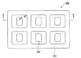
FIG. 1 is a cross-sectional view showing an example of a mask according to an embodiment of the present invention. FIG. 2 is a plan view of the mask shown in FIG. That is, FIG. 1 is a cross-sectional view of the position AA ′ in the
本実施形態のマスク100は、シリコン基板101で構成されている。シリコン基板101は、例えば面方位(100)を有することとする。そして、シリコン基板101には貫通孔をなす開口部102が設けられる。開口部102は、蒸着時に、蒸着源から出射された蒸着物質が通り抜ける貫通孔をなすものである。したがって、開口部102の開口領域は、被成膜部材(ガラス基板など)にパターニングする薄膜の形状とほぼ同一形状となっている。
The
また、開口部102の内側側面はテーパー形状となっている。このテーパー形状の開口部102における小さい開口側、すなわちシリコン基板101の面方位(100)の反対側面を、蒸着時に、被成膜部材に密着させるようにすることが好ましい。このようにすると、蒸着源とマスク100および被成膜部材とが相対的に移動したような場合でも、マスク100において、蒸着物質に対して影になるときと影にならないときとが生じる部位を低減でき、高精度の寸法に且つ均一な膜厚にパターニングすることができる。なお、図1および図2に示すマスク100では、開口部102が6個であるが本発明はこの構成に限定されず、開口部102の個数、形状および配置は任意とすることができる。
The inner side surface of the
また、本実施形態のマスク100では、シリコン基板101における全てのコーナー部すなわち角部位に、丸みRが形成されている。換言すれば、シリコン基板101の開口部102を含む全ての角部位は、直角又は鋭角になっておらず、応力の集中を緩和する構造となっている。ここで、マスク100における開口部102の角部位についてのみ、後述するように0.5μm以上であって3μm以下となる半径を有する大きさからなる丸みRが形成されている。また、図1及び図2に示すように、丸みRは、シリコン基板101の断面形状および平面形状の両方に持たせられている。シリコン基板101についてあらゆる角度から立体的に見て、直角又は鋭角になっているコーナー部が存在しない構成となっている。したがって、マスク100に対して任意の方向から応力が作用しても、その応力の集中を緩和できる構造となっている。
Further, in the
図3は、本発明の実施形態の変形例に係るマスクを示す断面図である。本変形例のマスク200は、シリコン基板201で構成されている。シリコン基板201は、例えば面方位(110)を有することとする。そして、シリコン基板201には貫通孔をなす開口部202が設けられる。マスク200とマスク100との主な相違点は、開口部202の内側側面の形状である。すなわち、開口部202の内側側面は、テーパー形状を有しておらず、マスク200の表面および裏面に対してほぼ垂直に形成されている。
FIG. 3 is a cross-sectional view showing a mask according to a modification of the embodiment of the present invention. The
マスク200のその他の構成は、マスク100と同様である。すなわち、マスク200は、シリコン基板201における全てのコーナー部すなわち角部位に、後述する大きさからなる丸みRが形成されている。したがって、マスク200は、開口部202を含む全ての角部位について、応力の集中を緩和する構造となっている。
Other configurations of the
従来、シリコン基板などからなる蒸着マスク(従来の蒸着マスク)は、通常、結晶異方性エッチングを用いて開口部などを形成している。これにより、従来の蒸着マスクは、開口部などの角部位が直角になっており、丸みRを付けることができなかった。そのため、従来の蒸着マスクでは、角部位に応力集中が発生し易く、その応力集中が発生した部分より亀裂が伝播して割れてしまうことが多々あった。また、従来の蒸着マスクの開口部は、被成膜部材(基板)に接する部分が54.7度の角度で鋭利な刀のように尖っており、この部分が基板にキズを付けて不良品を多発させるおそれもあった。 Conventionally, a vapor deposition mask (conventional vapor deposition mask) made of a silicon substrate or the like usually forms an opening or the like by using crystal anisotropic etching. As a result, the conventional vapor deposition mask has corner portions such as openings formed at right angles, and the roundness R cannot be applied. For this reason, in conventional vapor deposition masks, stress concentration is likely to occur at corner portions, and cracks often propagate from the portions where the stress concentration occurs and break. Moreover, the opening part of the conventional vapor deposition mask is pointed like a sharp sword at an angle of 54.7 degrees at the part in contact with the deposition target member (substrate), and this part is damaged by scratching the substrate. May also occur frequently.
本実施形態のマスク100,200によれば、開口部102,202を含む全ての角部位について、後述する0.5μm以上であって3μm以下となる半径を有する丸みRを付与しているので、開口部102,202を含む全ての角部位について、応力集中を緩和することができ、破損などの発生を大幅に低減することができる。
また、本実施形態のマスク100,200は、開口部102,202にも丸みRを付与しているので、被成膜部材に接する部分であって上記鋭利な刀のように尖っている部分が存在しない。したがって、本実施形態のマスク100,200は、被成膜部材にキズを付けることなくマスク蒸着できるので、歩留まりを向上させることができる。
According to the
In addition, since the
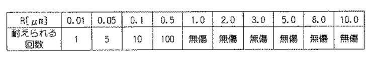
次に、丸みRの大きさについて述べる。
図4は、丸みRの大きさとマスク100,200の耐久性との関係を示す図である。図4においては、丸みRの半径が0.01μmから10.0μmまで段階的に異なる10種類のマスク100,200を試作して、耐久試験を行った結果を示している。すなわち、各種類のマスクについて、実際にマスク蒸着を繰り返し行い、そのマスクに破損(キズ)が生じたかなどを試験したものである。
Next, the size of the roundness R will be described.
FIG. 4 is a diagram showing the relationship between the size of the roundness R and the durability of the
例えば、丸みRの半径が0.01μmのマスク100,200の場合、1回のマスク蒸着で破損している。丸みRの半径が0.5μmのマスク100,200の場合、100回のマスク蒸着で破損が生じている。したがって、丸みRの半径が0.5μmのマスク100,200は、例えば100台の装置の製造に用いることができる。一方、丸みRの半径が1.0μm以上のマスク100,200の場合、1000回以上マスク蒸着をしても無傷である。したがって、丸みRの半径が1.0μm以上のマスク100,200は、大量生産される装置の製造に用いることができる。
For example, in the case of the
これらの耐久試験結果より、丸みRの半径を大きくするほどマスク100,200の耐久性が向上することがわかるとともに、丸みRの半径は0.5μm以上あることが好ましいことがわかる。
From these durability test results, it is understood that the durability of the
ただし、丸みRの半径を大きくしていくと、十分な寸法精度をもった蒸着パターンを形成することが困難となる。これは、丸みRの半径を大きくすると、開口部102,202の内部側面に形成されるオーバーハング(逆テーパ部)が大きくなり、蒸着物質に対して影になるときと影にならないときとが生じる部位が大きくなることなどのためである。そこで、例えば、丸みRの半径を3μm以下とすることにより、ある程度十分な寸法精度をもった蒸着パターンを形成できる。
However, when the radius of the roundness R is increased, it becomes difficult to form a vapor deposition pattern having sufficient dimensional accuracy. This is because when the radius of the roundness R is increased, an overhang (reverse taper portion) formed on the inner side surfaces of the
これらにより、本実施形態のマスク100,200は、丸みRの半径を0.5μm以上、3μm以下とすることで、蒸着パターンの寸法精度向上とマスクの機械的強度向上とを十分に両立させることができる。
As a result, the
(マスクの製造方法)
図5は、本発明の実施形態に係るマスクの製造方法を示すフローチャートである。本マスクの製造方法を用いることにより、例えば図1から図3に示すマスク100,200を製造することができる。以下、本マスクの製造方法について具体的に説明する。
(Manufacturing method of mask)
FIG. 5 is a flowchart showing a mask manufacturing method according to an embodiment of the present invention. By using this mask manufacturing method, for example, the
先ず、マスクの構成部材とするシリコン基板に対して、該シリコン基板を貫通する開口部を形成する開口部形成工程を実施する(ステップS1)。
例えば、ステップS1としては、所定形状のシリコンウエハーを用意し、そのシリコンウエハーに対して結晶異方性エッチングなどを施すことで開口部を形成する。結晶異方性エッチングをすると、寸法的に高精度に開口部を形成できるが、その開口部の角部位(コーナー部)が直角又は刀のように鋭角に尖ってしまう。
First, an opening forming process for forming an opening penetrating the silicon substrate is performed on the silicon substrate as a constituent member of the mask (step S1).
For example, as step S1, a silicon wafer having a predetermined shape is prepared, and an opening is formed by performing crystal anisotropic etching or the like on the silicon wafer. When crystal anisotropic etching is performed, an opening can be formed with high precision in dimension, but a corner portion (corner portion) of the opening is sharpened at a right angle or an acute angle like a sword.
次いで、開口部を含むシリコン基板全体における角部位について、丸み(R)を形成する丸み形成工程を実施する(ステップS2)。
ステップS2は、例えば等方性エッチングによって、簡便に且つ良好に実現できる。具体的には、開口部形成工程を経たシリコン基板を、ふっ酸(電子工業用;純度50%)100mlと硝酸(電子工業用;純度61%)2500mlと酢酸(電子工業用)1000mlとを混合させたエッチング液(温度25℃)に1分〜3分侵漬する。これだけで、ステップS2が良好に実行できる。そして、丸みRの半径は、エッチング時間により調節することができ、例えば上述した0.5μm以上3μm以下に形成する。
Next, a rounding process for forming roundness (R) is performed on corner portions of the entire silicon substrate including the opening (step S2).
Step S2 can be easily and satisfactorily realized by, for example, isotropic etching. Specifically, 100 ml of hydrofluoric acid (for the electronics industry;
すなわち、本侵漬によれば、シリコン基板の角部位について、硝酸(第1物質)によって酸化し、その酸化した物をふっ酸(第2物質)で除去することができる。さらに、本侵漬によれば、酢酸によってシリコン基板の露出面の粗さを低減することができる。したがって、本製造方法によれば、被成膜部材に対して良好に密着できて、より高精度の寸法に薄膜パターンを形成でき、機械的強度が高いマスクを簡便に製造することができる。 That is, according to this immersion, the corner portion of the silicon substrate is oxidized with nitric acid (first substance), and the oxidized product can be removed with hydrofluoric acid (second substance). Furthermore, according to this immersion, the roughness of the exposed surface of the silicon substrate can be reduced by acetic acid. Therefore, according to this manufacturing method, it is possible to easily manufacture a mask that can be satisfactorily adhered to the deposition target member, can form a thin film pattern with a more accurate dimension, and has high mechanical strength.
また、ステップS2は、ドライエッチングによる等方性エッチングで実現することもできる。例えば、SF6ガス、CF系ガスおよび塩素系ガスのうちのいずれかのガスを用いて、シリコン基板をドライエッチングすることで、等方性エッチングとなる。より具体的には、開口部形成工程を経たシリコン基板をプラズマエッチャーに入れ、SF6ガスを流しながらプラズマでエッチングする。このようなドライエッチングでも、丸みRの半径はエッチング時間により調節できる。 Step S2 can also be realized by isotropic etching by dry etching. For example, isotropic etching is achieved by dry etching the silicon substrate using any one of SF6 gas, CF gas, and chlorine gas. More specifically, the silicon substrate that has undergone the opening forming step is placed in a plasma etcher and etched with plasma while flowing SF6 gas. Even in such dry etching, the radius of the roundness R can be adjusted by the etching time.
上記丸み形成工程S2は、マスクの製造工程における最終工程として行うことが好ましい。このようにすると、シリコン基板からなるマスクの製造過程(開口部形成工程S1など)において、そのシリコン基板に角部位が形成されても、そのマスクの製造過程における最終段階で、かかる角部位について丸みを持たせることができる。換言すれば、シリコン基板からなるマスクの角部位(鋭角部又は直角部)を、簡便に且つ取りこぼしなく、丸めることができる。したがって、本実施形態によれば、高精度の寸法に薄膜パターンを形成でき、繰り返し使用されても容易に角部位などが破損しないマスクを、簡便に製造することができる。 The rounding step S2 is preferably performed as a final step in the mask manufacturing process. In this way, even if a corner portion is formed on the silicon substrate in the manufacturing process of the mask made of the silicon substrate (such as the opening forming step S1), the corner portion is rounded at the final stage of the mask manufacturing process. Can be given. In other words, the corner portion (acute angle portion or right angle portion) of the mask made of the silicon substrate can be rounded easily and without being overlooked. Therefore, according to the present embodiment, a thin film pattern can be formed in a highly accurate dimension, and a mask that does not easily break corner portions and the like even when used repeatedly can be easily manufactured.
また、本実施形態のマスクの製造方法では、マスクを用いたパターニングの形状精度を重視するときは形状精度を重視しないときよりも丸みRの半径を小さくし、マスクの機械的な耐久性を重視するときは、耐久性を重視しないときよりも丸みRの半径を大きくすることが好ましい。このようにすると、角部位の丸みの半径を小さくすることで、高いパターニング精度が要求されるマスクを製造できる。また、角部位の丸みの半径を大きくすることで、高い機械的強度が要求されるマスク(例えば大画面ディスプレイ基板用又は大量生産用)を製造できる。 Further, in the mask manufacturing method of this embodiment, when emphasizing the shape accuracy of patterning using a mask, the radius of the roundness R is made smaller than when not emphasizing the shape accuracy, and the mechanical durability of the mask is emphasized. When doing so, it is preferable to make the radius of the roundness R larger than when durability is not important. In this way, a mask that requires high patterning accuracy can be manufactured by reducing the radius of roundness at the corners. Further, by increasing the radius of roundness at the corners, a mask (for example, for a large screen display substrate or for mass production) that requires high mechanical strength can be manufactured.
(応用例)
次に、本実施形態の応用例について、図6から図16を参照して説明する。
図6は、本実施形態の応用例に係るマスクを示す模式斜視図である。図7は、図6に示すマスクによって形成される画素パターンの配列例を示す図である。図8は、図6に示すマスクの要部拡大斜視図である。本実施形態のマスク1は、図1から図3に示す上記実施形態のマスク100,200を構成要素とするものである。すなわち、マスク1におけるチップ20として、マスク100,200を用いる。本実施形態のマスク1は、例えば蒸着マスクとして用いることができる。
(Application examples)
Next, application examples of this embodiment will be described with reference to FIGS.
FIG. 6 is a schematic perspective view showing a mask according to an application example of the present embodiment. FIG. 7 is a diagram showing an example of the arrangement of pixel patterns formed by the mask shown in FIG. FIG. 8 is an enlarged perspective view of a main part of the mask shown in FIG. The
マスク1は、ベース基板をなす支持基板10に、複数のチップ20(マスク100,200)を取り付けた構成を有している。各チップ20は、それぞれアライメントされて支持基板10に接着されている。また、支持基板10には、マスク位置決めマーク16が形成されている。マスク位置決めマーク16は、マスク1を使用して蒸着などを行うときに、当該マスク1の位置合わせを行うためのものである。マスク位置決めマーク16は、例えば金属膜で形成することができる。なお、チップ20にマスク位置決めマーク16を形成してもよい。
The
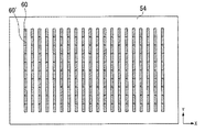
支持基板10には、開口部が長方形の貫通穴からなる開口領域12が、図6および図8に示すように、複数平行に且つ一定間隔で設けられている。チップ20には、図8に示すように、長孔形状の開口部22(開口部102,202に相当)が複数一定間隔で平行に設けられている。チップ20の開口部22は、図7に示す「縦ストライプ」の画素配置をなす薄膜パターンに対応する形状である。したがって、マスク1は、縦ストライプの画素を形成するために用いられる。
As shown in FIGS. 6 and 8, the
そして、各チップ20は、支持基板10の開口領域12をふさぐように、且つ、開口領域12の長手方向とチップ20の開口部22の長手方向とが直交する向きで、支持基板10上に行列をなすように配置されている。
Each
支持基板10の構成材料は、チップ20の構成材料の熱膨張係数と同一又は近い熱膨張係数を有するものが好ましい。チップ20はシリコンであるので、シリコンの熱膨張係数と同一又は近い熱膨張係数をもつ材料で支持基板10を構成する。このようにすることにより、支持基板10とチップ20との熱膨張量の違いによる「歪み」又は「橈み」の発生を抑えることができる。例えば、シリコンの熱膨張係数(30×10E-7/℃)に対して、コーニング社製のパイレックス(登録商標)ガラスの熱膨張係数(30×10E-7/℃)はほぼ同一値である。無アルカリガラスである日本電気ガラス社製のOA−10の熱膨張係数(38×10E-7/℃)、金属材料では42アロイの熱膨張係数(50×10E-7/℃)およびインバー材の熱膨張係数(12×10E-7/℃)などもシリコンの熱膨張係数に近い。したがって、支持基板10の構成材料としては、パイレックス(登録商標)ガラス、無アルカリガラスであるOA−10および42アロイなどが適用できる。
The constituent material of the
チップ20は、図8に示すように長方形の板に開口部22を設けた構成となっている。本実施形態のマスク1は図7に示す「縦ストライプ」の画素を形成するためのものであるので、チップ20の開口部22は例えばその画素を縦に40個ほど含む領域に相当する大きさの細長い溝形状となっている。すなわち、チップ20の開口部22は、被成膜面に形成される薄膜パターンの少なくとも一部の形状に対応した形状となっている。そして、チップ20が占有する面積は、マスク1で形成される薄膜パターン(例えば有機ELパネルを構成する薄膜パターン)の面積よりも小さい。
The
また、本実施形態のチップ20をなすシリコンは、面方位(110)を有している。ただし、面方位(100)を有するシリコンでチップ20を構成してもよい。そして、チップ20における開口部22の長手方向の側面は、面方位(111)を有している。このように開口部22の側面の面方位を(111)とすることは、面方位(110)を有するシリコンチップについて結晶異方性エッチングを施すことで簡便に実現できる。また、前記結晶異方性エッチングを施したシリコンチップについて等方性エッチングを施すことで、シリコンでチップ20における開口部22を含む全ての角部位について、丸みRを付与している。
Further, the silicon forming the
また、各チップ20にはアライメントマーク14が少なくとも2ヶ所形成されている。アライメントマーク14は、支持基板10にチップ20を貼り合わせる際の位置合わせに使用される。アライメントマーク14は、フォトリソグラフィ技術又は結晶異方性エッチングなどで形成する。
Each
チップ20における開口部20の長手方向と支持基板10の開口領域12の長手方向とが直交するように、各チップ20は支持基板10に貼り付けられている。開口部20の幅は、例えば画素のサブピクセルピッチd1と同一とする。そして、同一の開口領域12をふさぐチップ20であって隣り合うチップ20a,20bは、画素のサブピクセルピッチd1だけ間隔をもって配置されている。このチップ20aと20bとの隙間は、チップ20の開口部20と同様に機能し、所望形状の薄膜パターンを形成するためのマスク1の開口部として機能する。また、隣り合うチップ20同士は、開口領域12の長手方向に直交する方向についても間隔をもって配置されている。そして、複数のチップ20はそれぞれ間隔をもって、支持基板10上において、図6に示すように行列に配置されている。
Each
これらのように、本実施形態のマスク1は、複数のチップ20を支持基板10に取り付けているので、チップ20よりも大きな薄膜パターンを形成でき、例えば大画面の表示パネルをなす縦ストライプパターンの画素を形成することができる。さらに、本実施形態のマスク1は、シリコンでチップ20における開口部22を含む全ての角部位について丸みRを付与しているので、耐久性が高く、被成膜部材にキズを付けることを回避できる。
As described above, since the
図9は、図6および図8に示すマスク1を用いて形成された蒸着パターン(薄膜パターン)の一例を示す平面図である。図10は、図9に示す蒸着パターンが形成された基板について、マスク1をずらして再度蒸着処理を施した状態の一例を示す平面図である。図11は、図10に示す蒸着パターンが形成された基板について、マスク1をずらして再度蒸着処理を施した状態の一例を示す平面図である。
FIG. 9 is a plan view showing an example of a vapor deposition pattern (thin film pattern) formed using the
この蒸着パターンが形成される被成膜部材をなす基板54としては、例えば有機EL装置の構成要素をなすガラス基板などの透明基板を適用できる。この場合の蒸着パターンは、例えば有機EL装置における赤色の発光層60をなすストライプパターンとする。したがって、発光層60の幅は画素のサブピクセルピッチd1となっている。
For example, a transparent substrate such as a glass substrate that is a constituent element of an organic EL device can be applied as the
ただし、図9に示す蒸着パターンでは、有機EL装置の赤色の画素における複数行(例えば40行×5)の画素が形成されていない。そこで、基板54に対してマスク1を縦方向(Y軸方向)に例えば画素40個分だけずらして、再度蒸着処理を行い、図10に示すように赤色の発光層60’をパターニングする。このようにすることにより、大きな縦ストライプパターンを持った大画面パネルの薄膜パターンを簡便に形成することができる。
However, in the vapor deposition pattern shown in FIG. 9, pixels of a plurality of rows (for example, 40 rows × 5) in the red pixels of the organic EL device are not formed. Therefore, the
図10に示す蒸着パターンでは、赤色の発光層60,60’のみが形成されており、緑色及び青色の発光層が形成されていない。そこで、図10に示す状態の基板54に対して、マスク1を横方向(X軸方向)にサブピクセルピッチ分だけずらして緑色の発光材料をパターニングすることで、図11に示すように、緑色の発光層62を形成する。次いで、マスク1を横方向(X軸方向)にサブピクセルピッチ分だけずらして青色の発光材料をパターニングすることで、図11に示すように、青色の発光層64を形成する。
In the vapor deposition pattern shown in FIG. 10, only the red
これらにより、カラー表示ができて大画面パネルをなす薄膜パターンを、簡便に、高精度に、且つ低コストで形成することができる。また、上記実施形態では同一のマスク1をずらしながら複数回蒸着処理することで1つの大画面パネルをなす薄膜パターンを形成しているが、複数種類のマスク1を予め作成して、その複数種類のマスク1を交互に用いて1つの大画面パネルをなす薄膜パターンを形成してもよい。
As a result, a thin film pattern capable of color display and forming a large screen panel can be formed simply, with high accuracy, and at low cost. Further, in the above embodiment, the thin film pattern forming one large screen panel is formed by performing the vapor deposition process a plurality of times while shifting the
図12は、本実施形態のマスクの製造方法を示す模式断面図である。すなわち、図12は上記マスク1の主要部をなすシリコンのチップ20の製造方法を示している。
先ず、面方位(110)のシリコンウエハー20’を用意し、熱酸化法により耐エッチングマスク材となる酸化シリコン膜71をそのシリコンウエハー20’の露出面全体に1μm厚に形成する(図12(a)参照)。
この酸化シリコン膜71からなる耐エッチングマスク材は、後の工程でアルカリ水溶液を用いて行われる結晶異方性エッチングにおいて耐久性のある膜であればよい。したがって、かかる耐エッチングマスク材は、CVD法で設けられた窒化シリコン膜としてもよく、スパッター法で設けられたAu又はPt膜などでもよく、特に酸化シリコン膜に限定されるものではない。
FIG. 12 is a schematic cross-sectional view showing the mask manufacturing method of the present embodiment. That is, FIG. 12 shows a method of manufacturing the
First, a
The etching resistant mask material made of the
次いで、上記シリコンウエハー20’の一方面側の酸化シリコン膜71について、フォトリソグラフィ技術を用いてパターニングすることで、上記開口部22の開口形状(断面形状)に対応する形状の溝パターン72を形成する。ここで、シリコンの(111)方位と溝パターン72の長手方向とが直角になるように、その溝パターン72を形成する(図12(b)参照)。
また、上記溝パターン72の形成と同時に、アライメントマーク14をシリコンウエハー20’に形成してもよい。
Next, the
The
また、上記溝パターン72の形成と同時に、シリコンウエハー20’の他方面側の酸化シリコン膜71について、上記フォトリソグラフィ工程により、上記開口部22に対応する部分を含む大きな領域73を除去する(図12(b)参照)。
このように、シリコンウエハー20’の他方面側の酸化シリコン膜71における領域73を除去するのは、後の工程により、シリコンウエハー20’における開口部22を含む領域の厚みd2を小さくするためである。すなわち、シリコンウエハー20’から形成されるチップ20を薄くして、蒸着時に蒸着粒子が開口部22を斜め方向に通過し易くして、成膜される薄膜の厚さを均一化するためである。
酸化シリコン膜71についてのフォトリソグラフィ技術によるパターニングでは、例えば緩衝ふっ酸溶液を用いる。
Simultaneously with the formation of the
Thus, the
For patterning the
次いで、図12(b)に示す状態のシリコンウエハー20’について、80℃に加熱した35重量%の水酸化カリウム水溶液を用いて結晶異方性エッチングを行う。この結晶異方性エッチングにより、シリコンウエハー20’における酸化シリコン膜71に覆われていない部分は、一方面および他方面の両側から除去されていき、開口部22をなす貫通溝を形成するとともに、開口部22を含む領域の厚みd2を小さくする。また、この結晶異方性エッチングにより、シリコンウエハー20’の領域73側の角部74もエッチングされて、テーパー形状となる(図12(c)参照)。
Next, crystal anisotropic etching is performed on the
上記結晶異方性エッチングのエッチング時間を制御することにより、角部74のテーパー形状および開口部22を含む領域の厚みd2を管理することができる。したがって、マスク1と蒸着源との相対的な位置関係が変動しても、マスク1の影の領域が変化しない良好なマスクを製造することができる。
By controlling the etching time of the crystal anisotropic etching, the tapered shape of the
次いで、シリコンウエハー20’に形成されている酸化シリコン膜71を除去することで、開口部22を有するチップ20を形成する(図12(d)参照)。
この酸化シリコン膜71の除去では、例えば緩衝ふっ酸溶液を用いる。
これらの図12(a)から図12(d)に示す工程は、図5に示す開口部形成工程S1に相当する。そこで、図12(d)の工程の後に、図5に示す丸み形成工程を実施して、マスク1の構成要素となるチップ20を完成させる。すなわち、図12(d)の工程の後に、チップ20について、所定時間だけ等方性エッチングを施す。
Next, the
In removing the
The steps shown in FIGS. 12A to 12D correspond to the opening forming step S1 shown in FIG. Therefore, after the step of FIG. 12D, the round forming step shown in FIG. 5 is performed to complete the
これらにより、本実施形態の製造方法によれば、チップ20の開口部22について結晶異方性エッチングを用いて形成するので、開口部22の形状について高精度に加工することができる。また、本製造方法は、前記結晶異方性エッチングの後に等方性エッチングを施してチップ20のすべての角部位に丸みRを付与するので、高精度の寸法に薄膜パターンを形成でき、繰り返し使用されても容易に角部位などが破損しないチップ20を、簡便に製造することができる。
Thus, according to the manufacturing method of the present embodiment, the
(電気光学装置の製造方法)
図13は、本発明の実施形態に係る電気光学装置の製造方法を示す模式断面図である。本実施形態では、電気光学装置の一つとして有機EL装置を挙げて説明する。図13に示すマスク50(上記マスク1に該当する)には、磁性体膜52が形成されている。磁性体膜52は、鉄、コバルト、ニッケル等の強磁性材料で形成することができる。あるいは、Ni、Co、Feや、Fe成分を含むステンレス合金等の磁性金属材料や、磁性金属材料と非磁性金属材料との結合により、磁性体膜52を形成してもよい。マスク50のその他の詳細は、上記マスク1と同一である。
(Method for manufacturing electro-optical device)
FIG. 13 is a schematic cross-sectional view illustrating the method for manufacturing the electro-optical device according to the embodiment of the invention. In this embodiment, an organic EL device will be described as one of electro-optical devices. A
本実施形態では、マスク50を使用して基板(成膜対象部材)54に発光材料を成膜する。基板54は、複数の有機EL装置を形成するためのもので、ガラス基板等の透明基板である。基板54には、図14(A)に示すように、電極(例えばITO等からなる透明電極)56および正孔輸送層58が形成されている。なお、電子輸送層を形成してもよい。
In this embodiment, a light emitting material is formed on the substrate (film formation target member) 54 using the
図13に示すように、基板54側にチップ20が位置するように、マスク50を配置する。基板54の背後には、磁石48が配置されており、マスク50(チップ20)に形成された磁性体膜52を引き寄せるようになっている。
As shown in FIG. 13, the
図14(A)〜図14(C)は、有機EL装置の製造に用いられる発光材料の成膜方法を説明する模式断面図である。発光材料は、例えば有機材料であり、低分子の有機材料としてアルミキノリノール錯体(Alq3)があり、高分子の有機材料としてポリパラフェニレンビニレン(PPV)がある。発光材料の成膜は、蒸着によって行うことができる。例えば、図14(A)に示すように、マスク50を介して赤色の発光材料をパターニングしながら成膜し、赤色の発光層60を形成する。そして、図14(B)に示すように、マスク50をずらして、緑色の発光材料をパターニングしながら成膜し、緑色の発光層62を形成する。そして、図14(C)に示すように、マスク50を再びずらして、青色の発光材料をパターニングしながら成膜し、青色の発光層64を形成する。
14A to 14C are schematic cross-sectional views illustrating a method for forming a light-emitting material used for manufacturing an organic EL device. The light-emitting material is, for example, an organic material, such as an aluminum quinolinol complex (Alq 3 ) as a low molecular organic material, and polyparaphenylene vinylene (PPV) as a high molecular organic material. The light-emitting material can be formed by vapor deposition. For example, as shown in FIG. 14A, a red
本実施形態では、スクリーンとなるチップ20が、支持基板10に部分的に接着されている。したがって、チップ20は自由度が高く、反り、撓みが発生し難く、機械的強度が高く、選択蒸着の再現性が高く、生産性が高い。本実施形態のマスク50では、支持基板10に複数の開口領域12が形成され、それぞれの開口領域12に対応してチップ20が位置している。複数のチップ20が1つの有機EL装置に対応する。すなわち、マスク50を使用して、大画面の有機EL装置を高精度に且つ低コストで製造することができる。
In this embodiment, the
図15は、上述した発光材料の成膜方法を経て製造された有機EL装置の概略構成を示す模式断面図である。有機EL装置は、基板54、電極56、正孔輸送層58、発光層60,62,64などを有する。発光層60,62,64上には、電極66が形成されている。電極66は、例えば陰極電極である。本実施形態の有機EL装置は、表示装置(ディスプレイ)として好適であり、発光層60,62,64においてパターンずれが少なく膜厚分布が非常に均一化され、ムラの無い鮮やかな大画面の表示装置となることができ、さらに低コストで提供できる。
FIG. 15 is a schematic cross-sectional view showing a schematic configuration of an organic EL device manufactured through the above-described method for forming a light emitting material. The organic EL device includes a
(電子機器)
次に上記実施形態のマスクを用いて製造された電子機器について説明する。
図16(a)は、携帯電話の一例を示した斜視図である。図16(a)において、符号600は携帯電話本体を示し、符号601は上記実施形態のマスクを用いて形成された電気光学装置からなる表示部を示している。図16(b)は、ワープロ、パソコンなどの携帯型情報処理装置の一例を示した斜視図である。図16(b)において、符号700は情報処理装置、符号701はキーボードなどの入力部、符号702は上記実施形態のマスクを用いて形成された電気光学装置からなる表示部、符号703は情報処理装置本体を示している。図16(c)は、腕時計型電子機器の一例を示した斜視図である。図16(c)において、符号800は時計本体を示し、符号801は上記実施形態のマスクを用いて形成された電気光学装置からなる表示部を示している。
(Electronics)
Next, an electronic device manufactured using the mask of the above embodiment will be described.
FIG. 16A is a perspective view showing an example of a mobile phone. In FIG. 16A,
図16に示す電子機器は、大画面で表示でき、鮮やかでムラがなく大きな画像を高品位に表示でき、さらに、低コストで製造することができる。 The electronic device illustrated in FIG. 16 can be displayed on a large screen, can display a large image with high brightness without being uneven, and can be manufactured at low cost.
なお、本発明の技術範囲は上記実施形態に限定されるものではなく、本発明の趣旨を逸脱しない範囲において種々の変更を加えることが可能であり、実施形態で挙げた具体的な材料や層構成などはほんの一例に過ぎず、適宜変更が可能である。例えば、上記実施形態ではマスク1,100,200を蒸着マスクとして用いたが、本発明はこれに限定されるものではなく、スパッター法又はCVD法などにおけるマスクとしてマスク1,100,200を用いることができる。
The technical scope of the present invention is not limited to the above-described embodiment, and various modifications can be made without departing from the spirit of the present invention, and the specific materials and layers mentioned in the embodiment can be added. The configuration is merely an example, and can be changed as appropriate. For example, in the above embodiment, the
1,100,200…マスク、10…支持基板、12…開口領域、20…チップ、20’…シリコンウエハー、22,102,202…開口部、101,201…シリコン基板、R…丸み
DESCRIPTION OF SYMBOLS 1,100,200 ... Mask, 10 ... Support substrate, 12 ... Opening area, 20 ... Chip, 20 '... Silicon wafer, 22, 102, 202 ... Opening part, 101, 201 ... Silicon substrate, R ... Roundness
Claims (14)
前記開口部は、前記パターニングするときに前記物質が前記マスクを通り抜ける貫通孔をなすものであることを特徴とする請求項1に記載のマスク。 The mask is disposed between a film forming member and a kimono source that emits a substance when a thin film is patterned on the film forming member.
The mask according to claim 1, wherein the opening forms a through hole through which the substance passes through the mask when the patterning is performed.
前記開口部における角部位について、丸みを形成する丸み形成工程とを有することを特徴とするマスクの製造方法。 An opening forming step of forming an opening penetrating the silicon substrate with respect to the silicon substrate as a constituent member of the mask;
A method of manufacturing a mask, comprising: a roundness forming step of forming roundness at a corner portion in the opening.
マスクの機械的な耐久性を重視するときは、該耐久性を重視しないときよりも前記丸みの半径を大きくすることを特徴とする請求項4から11のいずれか一項に記載のマスクの製造方法。 When emphasizing the shape accuracy of patterning using a mask, the radius of the roundness is made smaller than when not emphasizing the shape accuracy,
The mask manufacturing method according to any one of claims 4 to 11, wherein when the mechanical durability of the mask is regarded as important, the radius of the roundness is made larger than when the durability is not regarded as important. Method.
Priority Applications (6)
| Application Number | Priority Date | Filing Date | Title |
|---|---|---|---|
| JP2004104311A JP3765314B2 (en) | 2004-03-31 | 2004-03-31 | Mask, mask manufacturing method, electro-optical device manufacturing method, and electronic apparatus |
| EP05006370A EP1583400A2 (en) | 2004-03-31 | 2005-03-23 | Mask, method for manufacturing a mask, method for manufacturing an electro-optical device, and electronic equipment |
| KR1020050026423A KR100707553B1 (en) | 2004-03-31 | 2005-03-30 | Mask, method for manufacturing a mask, method for manufacturing an electro-optical device, and electronic equipment |
| TW094110094A TWI263457B (en) | 2004-03-31 | 2005-03-30 | Mask, method for manufacturing a mask, method for manufacturing an electro-optical device, and electronic equipment |
| US11/093,840 US7285497B2 (en) | 2004-03-31 | 2005-03-30 | Mask, method for manufacturing a mask, method for manufacturing an electro-optical device, and electronic equipment |
| CNA2005100629508A CN1678145A (en) | 2004-03-31 | 2005-03-31 | Mask, method for manufacturing a mask, method for manufacturing an electro-optical device, and electronic equipment |
Applications Claiming Priority (1)
| Application Number | Priority Date | Filing Date | Title |
|---|---|---|---|
| JP2004104311A JP3765314B2 (en) | 2004-03-31 | 2004-03-31 | Mask, mask manufacturing method, electro-optical device manufacturing method, and electronic apparatus |
Publications (2)
| Publication Number | Publication Date |
|---|---|
| JP2005293917A JP2005293917A (en) | 2005-10-20 |
| JP3765314B2 true JP3765314B2 (en) | 2006-04-12 |
Family
ID=34880050
Family Applications (1)
| Application Number | Title | Priority Date | Filing Date |
|---|---|---|---|
| JP2004104311A Expired - Fee Related JP3765314B2 (en) | 2004-03-31 | 2004-03-31 | Mask, mask manufacturing method, electro-optical device manufacturing method, and electronic apparatus |
Country Status (6)
| Country | Link |
|---|---|
| US (1) | US7285497B2 (en) |
| EP (1) | EP1583400A2 (en) |
| JP (1) | JP3765314B2 (en) |
| KR (1) | KR100707553B1 (en) |
| CN (1) | CN1678145A (en) |
| TW (1) | TWI263457B (en) |
Families Citing this family (19)
| Publication number | Priority date | Publication date | Assignee | Title |
|---|---|---|---|---|
| JP3775493B2 (en) * | 2001-09-20 | 2006-05-17 | セイコーエプソン株式会社 | Mask manufacturing method |
| US7591955B2 (en) * | 2005-07-14 | 2009-09-22 | Interplex Nas, Inc. | Method for forming an etched soft edge metal foil and the product thereof |
| JP2007234678A (en) | 2006-02-27 | 2007-09-13 | Hitachi Displays Ltd | Organic el display |
| JP2009031561A (en) * | 2007-07-27 | 2009-02-12 | Adtec Engineeng Co Ltd | Projection exposure apparatus and division exposure method |
| JP5607312B2 (en) * | 2009-04-02 | 2014-10-15 | 株式会社ボンマーク | Vapor deposition mask and manufacturing method thereof |
| TWI464800B (en) * | 2011-06-16 | 2014-12-11 | Motech Ind Inc | Method for patterning surface of semiconductor substrate |
| JP5927786B2 (en) * | 2011-06-22 | 2016-06-01 | セイコーエプソン株式会社 | Substrate drilling method |
| CN103205704A (en) * | 2012-01-16 | 2013-07-17 | 昆山允升吉光电科技有限公司 | Vapor deposition mask |
| CN102931070B (en) * | 2012-11-09 | 2015-06-10 | 天水天光半导体有限责任公司 | Silicon substrate isotropic wet etching process |
| JP6060862B2 (en) * | 2013-09-13 | 2017-01-18 | コニカミノルタ株式会社 | Vapor deposition mask, vapor deposition mask manufacturing method, and organic electroluminescent element manufacturing method |
| JP2016046454A (en) * | 2014-08-26 | 2016-04-04 | 太陽誘電株式会社 | Thin film electronic component |
| EP3993075A1 (en) * | 2015-04-24 | 2022-05-04 | Lg Innotek Co. Ltd | Deposition mask |
| CN105803390A (en) * | 2016-05-20 | 2016-07-27 | 京东方科技集团股份有限公司 | Mask plate for depositing film layer, film layer and array substrate |
| WO2018066611A1 (en) * | 2016-10-06 | 2018-04-12 | 大日本印刷株式会社 | Method for producing vapor deposition mask, method for producing organic semiconductor element, and method for producing organic el display |
| JP2018170152A (en) * | 2017-03-29 | 2018-11-01 | Tianma Japan株式会社 | Manufacturing method of oled display device, mask and design method of mask |
| CN107686964A (en) * | 2017-08-24 | 2018-02-13 | 京东方科技集团股份有限公司 | Mask plate support frame and mask plate |
| CN108251794A (en) * | 2018-01-19 | 2018-07-06 | 昆山国显光电有限公司 | The post-processing approach and mask plate of mask plate |
| JP7110776B2 (en) * | 2018-07-11 | 2022-08-02 | 大日本印刷株式会社 | Vapor deposition mask, method for manufacturing vapor deposition mask, and method for manufacturing organic EL display device |
| JP2022071292A (en) * | 2020-10-28 | 2022-05-16 | キヤノン株式会社 | Vapor deposition mask, and production method of device using vapor deposition mask |
Family Cites Families (25)
| Publication number | Priority date | Publication date | Assignee | Title |
|---|---|---|---|---|
| JPS62297457A (en) | 1986-06-17 | 1987-12-24 | Fujitsu Ltd | Mask for vapor deposition |
| US5067985A (en) * | 1990-06-08 | 1991-11-26 | The United States Of America As Represented By The Secretary Of The Air Force | Back-contact vertical-junction solar cell and method |
| JPH04236758A (en) | 1991-01-16 | 1992-08-25 | Oki Electric Ind Co Ltd | Mask for vapor deposition |
| JPH10298738A (en) | 1997-04-21 | 1998-11-10 | Mitsubishi Chem Corp | Shadow mask and vapor depositing method |
| US5801083A (en) * | 1997-10-20 | 1998-09-01 | Chartered Semiconductor Manufacturing, Ltd. | Use of polymer spacers for the fabrication of shallow trench isolation regions with rounded top corners |
| KR19990051416A (en) * | 1997-12-19 | 1999-07-05 | 윤종용 | Method of forming an isolation layer in a semiconductor device using a rounded mask pattern |
| JP3862845B2 (en) * | 1998-02-05 | 2006-12-27 | セイコーインスツル株式会社 | Near-field optical probe |
| TW406350B (en) * | 1998-12-07 | 2000-09-21 | United Microelectronics Corp | Method for manufacturing the shallow trench isolation area |
| US6165906A (en) * | 1999-01-26 | 2000-12-26 | Advanced Micro Devices, Inc. | Semiconductor topography employing a shallow trench isolation structure with an improved trench edge |
| JP4020233B2 (en) * | 1999-08-25 | 2007-12-12 | セイコーインスツル株式会社 | Near-field optical head and manufacturing method thereof |
| JP2001118919A (en) * | 1999-10-15 | 2001-04-27 | Seiko Epson Corp | Semiconductor device and manufacturing method therefor |
| JP2001185350A (en) | 1999-12-24 | 2001-07-06 | Sanyo Electric Co Ltd | Worn mask, its manufacturing method, electroluminescent display device and its manufacturing method |
| JP2001273976A (en) | 2000-03-28 | 2001-10-05 | Tohoku Pioneer Corp | Organic electroluminescence display panel, its manufacturing method, and its deposition device |
| TW461025B (en) * | 2000-06-09 | 2001-10-21 | Nanya Technology Corp | Method for rounding corner of shallow trench isolation |
| US6524929B1 (en) * | 2001-02-26 | 2003-02-25 | Advanced Micro Devices, Inc. | Method for shallow trench isolation using passivation material for trench bottom liner |
| JP2002313564A (en) | 2001-04-17 | 2002-10-25 | Nec Corp | Shadow mask, method of manufacturing the shadow mask, and display |
| JP4046269B2 (en) | 2001-05-24 | 2008-02-13 | 九州日立マクセル株式会社 | Vapor deposition mask for organic EL element and method for producing vapor deposition mask for organic EL element |
| JP3775493B2 (en) | 2001-09-20 | 2006-05-17 | セイコーエプソン株式会社 | Mask manufacturing method |
| JP2003174082A (en) * | 2001-12-06 | 2003-06-20 | Mitsubishi Electric Corp | Semiconductor device and manufacturing method thereof |
| US6670279B1 (en) * | 2002-02-05 | 2003-12-30 | Taiwan Semiconductor Manufacturing Company | Method of forming shallow trench isolation with rounded corners and divot-free by using in-situ formed spacers |
| US6511902B1 (en) * | 2002-03-26 | 2003-01-28 | Macronix International Co., Ltd. | Fabrication method for forming rounded corner of contact window and via by two-step light etching technique |
| KR100813832B1 (en) | 2002-05-31 | 2008-03-17 | 삼성에스디아이 주식회사 | Mask frame assembly for an evaporation and method of manufacturing the same |
| JP2004043877A (en) | 2002-07-11 | 2004-02-12 | Canon Electronics Inc | Mask for vapor deposition, and organic electroluminescent display device |
| KR100967201B1 (en) * | 2003-02-05 | 2010-07-05 | 매그나칩 반도체 유한회사 | Method for forming isolation of semiconductor device |
| JP4369199B2 (en) | 2003-06-05 | 2009-11-18 | 九州日立マクセル株式会社 | Vapor deposition mask and manufacturing method thereof |
-
2004
- 2004-03-31 JP JP2004104311A patent/JP3765314B2/en not_active Expired - Fee Related
-
2005
- 2005-03-23 EP EP05006370A patent/EP1583400A2/en not_active Withdrawn
- 2005-03-30 KR KR1020050026423A patent/KR100707553B1/en not_active IP Right Cessation
- 2005-03-30 US US11/093,840 patent/US7285497B2/en not_active Expired - Fee Related
- 2005-03-30 TW TW094110094A patent/TWI263457B/en not_active IP Right Cessation
- 2005-03-31 CN CNA2005100629508A patent/CN1678145A/en active Pending
Also Published As
| Publication number | Publication date |
|---|---|
| US20050221609A1 (en) | 2005-10-06 |
| US7285497B2 (en) | 2007-10-23 |
| JP2005293917A (en) | 2005-10-20 |
| EP1583400A2 (en) | 2005-10-05 |
| KR20060045140A (en) | 2006-05-16 |
| CN1678145A (en) | 2005-10-05 |
| TWI263457B (en) | 2006-10-01 |
| TW200605713A (en) | 2006-02-01 |
| KR100707553B1 (en) | 2007-04-13 |
Similar Documents
| Publication | Publication Date | Title |
|---|---|---|
| KR100707553B1 (en) | Mask, method for manufacturing a mask, method for manufacturing an electro-optical device, and electronic equipment | |
| US7268406B2 (en) | Mask, mask chip, manufacturing method of mask, manufacturing method of mask chip, and electronic device | |
| JP4428285B2 (en) | Mask holding structure, film forming method, and electro-optical device manufacturing method | |
| US20050211981A1 (en) | Mask, method of manufacturing the same, method of forming thin film pattern, method of manufacturing electro-optical device and electronic equipment | |
| US6893575B2 (en) | Mask and method of manufacturing the same, electro-luminescence device and method of manufacturing the same, and electronic instrument | |
| KR100698033B1 (en) | Organic Electroluminescence Device and Fabrication Method for the same | |
| TWI244354B (en) | Deposition mask, manufacturing method thereof, display unit, manufacturing method thereof, and electronic apparatus including display unit | |
| KR100484023B1 (en) | Mask and manufacturing method thereof, and method of manufacturing electro-luminescence device | |
| US20050064622A1 (en) | Mask, method of manufacturing a mask, method of manufacturing an organic electroluminescence device, and organic electroluminiescence device | |
| JP2005165015A (en) | Mask for film deposition, film deposition device, electro-optical device, and electronic appliance | |
| JP2005206939A (en) | Thin film formation method, thin film formation equipment, method of manufacturing organic electroluminescence device, organic electroluminescence device, and electronic apparatus | |
| JP2002069619A (en) | Metal-mask structural body and its production method | |
| US7387739B2 (en) | Mask and method of manufacturing the same, electroluminescent device and method of manufacturing the same, and electronic instrument | |
| JP2010095744A (en) | Vapor deposition mask, method for manufacturing the mask, method for manufacturing electro-optical device, and electronic device | |
| JP2007035440A (en) | Mask manufacturing method, mask, film formation method, manufacturing method of electrooptical device and electronic apparatus | |
| JP2006077276A (en) | Mask, method for manufacturing mask, method for forming thin-film pattern, and method for manufacturing electro-optic device | |
| JP4235823B2 (en) | Mask manufacturing method | |
| JP2006077297A (en) | Mask, film deposition method and method for producing organic el system | |
| KR100463532B1 (en) | fabrication method for display panel using large scale full-color | |
| KR100267965B1 (en) | How to make shadow mask | |
| JP2004335486A (en) | Mask and its manufacturing method, electroluminescent device and its manufacturing method, and electronic equipment | |
| JP2005290524A (en) | Mask, method for producing mask, method for producing electro-optical apparatus and electronic equipment |
Legal Events
| Date | Code | Title | Description |
|---|---|---|---|
| A621 | Written request for application examination |
Free format text: JAPANESE INTERMEDIATE CODE: A621 Effective date: 20050728 |
|
| RD03 | Notification of appointment of power of attorney |
Free format text: JAPANESE INTERMEDIATE CODE: A7423 Effective date: 20050728 |
|
| A521 | Request for written amendment filed |
Free format text: JAPANESE INTERMEDIATE CODE: A821 Effective date: 20050729 |
|
| A871 | Explanation of circumstances concerning accelerated examination |
Free format text: JAPANESE INTERMEDIATE CODE: A871 Effective date: 20050831 |
|
| A975 | Report on accelerated examination |
Free format text: JAPANESE INTERMEDIATE CODE: A971005 Effective date: 20050916 |
|
| A131 | Notification of reasons for refusal |
Free format text: JAPANESE INTERMEDIATE CODE: A131 Effective date: 20051004 |
|
| A521 | Request for written amendment filed |
Free format text: JAPANESE INTERMEDIATE CODE: A523 Effective date: 20051202 |
|
| TRDD | Decision of grant or rejection written | ||
| A01 | Written decision to grant a patent or to grant a registration (utility model) |
Free format text: JAPANESE INTERMEDIATE CODE: A01 Effective date: 20060104 |
|
| A61 | First payment of annual fees (during grant procedure) |
Free format text: JAPANESE INTERMEDIATE CODE: A61 Effective date: 20060117 |
|
| R150 | Certificate of patent or registration of utility model |
Free format text: JAPANESE INTERMEDIATE CODE: R150 |
|
| FPAY | Renewal fee payment (event date is renewal date of database) |
Free format text: PAYMENT UNTIL: 20090203 Year of fee payment: 3 |
|
| FPAY | Renewal fee payment (event date is renewal date of database) |
Free format text: PAYMENT UNTIL: 20100203 Year of fee payment: 4 |
|
| FPAY | Renewal fee payment (event date is renewal date of database) |
Free format text: PAYMENT UNTIL: 20110203 Year of fee payment: 5 |
|
| FPAY | Renewal fee payment (event date is renewal date of database) |
Free format text: PAYMENT UNTIL: 20110203 Year of fee payment: 5 |
|
| FPAY | Renewal fee payment (event date is renewal date of database) |
Free format text: PAYMENT UNTIL: 20120203 Year of fee payment: 6 |
|
| FPAY | Renewal fee payment (event date is renewal date of database) |
Free format text: PAYMENT UNTIL: 20130203 Year of fee payment: 7 |
|
| FPAY | Renewal fee payment (event date is renewal date of database) |
Free format text: PAYMENT UNTIL: 20130203 Year of fee payment: 7 |
|
| LAPS | Cancellation because of no payment of annual fees |