JP3746719B2 - Flip chip mounting method - Google Patents
Flip chip mounting method Download PDFInfo
- Publication number
- JP3746719B2 JP3746719B2 JP2002075863A JP2002075863A JP3746719B2 JP 3746719 B2 JP3746719 B2 JP 3746719B2 JP 2002075863 A JP2002075863 A JP 2002075863A JP 2002075863 A JP2002075863 A JP 2002075863A JP 3746719 B2 JP3746719 B2 JP 3746719B2
- Authority
- JP
- Japan
- Prior art keywords
- bump
- gold
- circuit board
- chip mounting
- semiconductor element
- Prior art date
- Legal status (The legal status is an assumption and is not a legal conclusion. Google has not performed a legal analysis and makes no representation as to the accuracy of the status listed.)
- Expired - Fee Related
Links
Images


Classifications
-
- H—ELECTRICITY
- H01—ELECTRIC ELEMENTS
- H01L—SEMICONDUCTOR DEVICES NOT COVERED BY CLASS H10
- H01L2224/00—Indexing scheme for arrangements for connecting or disconnecting semiconductor or solid-state bodies and methods related thereto as covered by H01L24/00
- H01L2224/01—Means for bonding being attached to, or being formed on, the surface to be connected, e.g. chip-to-package, die-attach, "first-level" interconnects; Manufacturing methods related thereto
- H01L2224/10—Bump connectors; Manufacturing methods related thereto
- H01L2224/11—Manufacturing methods
- H01L2224/113—Manufacturing methods by local deposition of the material of the bump connector
- H01L2224/1133—Manufacturing methods by local deposition of the material of the bump connector in solid form
- H01L2224/1134—Stud bumping, i.e. using a wire-bonding apparatus
-
- H—ELECTRICITY
- H01—ELECTRIC ELEMENTS
- H01L—SEMICONDUCTOR DEVICES NOT COVERED BY CLASS H10
- H01L2224/00—Indexing scheme for arrangements for connecting or disconnecting semiconductor or solid-state bodies and methods related thereto as covered by H01L24/00
- H01L2224/01—Means for bonding being attached to, or being formed on, the surface to be connected, e.g. chip-to-package, die-attach, "first-level" interconnects; Manufacturing methods related thereto
- H01L2224/10—Bump connectors; Manufacturing methods related thereto
- H01L2224/12—Structure, shape, material or disposition of the bump connectors prior to the connecting process
- H01L2224/13—Structure, shape, material or disposition of the bump connectors prior to the connecting process of an individual bump connector
- H01L2224/13001—Core members of the bump connector
- H01L2224/13075—Plural core members
- H01L2224/1308—Plural core members being stacked
-
- H—ELECTRICITY
- H01—ELECTRIC ELEMENTS
- H01L—SEMICONDUCTOR DEVICES NOT COVERED BY CLASS H10
- H01L2224/00—Indexing scheme for arrangements for connecting or disconnecting semiconductor or solid-state bodies and methods related thereto as covered by H01L24/00
- H01L2224/80—Methods for connecting semiconductor or other solid state bodies using means for bonding being attached to, or being formed on, the surface to be connected
- H01L2224/81—Methods for connecting semiconductor or other solid state bodies using means for bonding being attached to, or being formed on, the surface to be connected using a bump connector
- H01L2224/8119—Arrangement of the bump connectors prior to mounting
- H01L2224/81191—Arrangement of the bump connectors prior to mounting wherein the bump connectors are disposed only on the semiconductor or solid-state body
Description
【0001】
【発明の属する技術分野】
本発明は、フリップチップ実装方法に関し、詳しくは、半導体素子と回路基板とを、多段バンプを用いて電気的に接続するフリップチップ実装方法に関するものである。
【0002】
【従来の技術】
従来、半導体素子を回路基板上に実装するフリップチップ実装方法としては、特開平8−1786号公報に開示されたものが知られている。
【0003】
同公報に開示されたフリップチップ実装方法により得られる実装形態は、図8に示すように、半導体素子を含むパッケージ101、そのパッケージ101上の電極102、はんだバンプ103a、はんだバンプ103b、樹脂104、回路基板105、回路基板105上の電極106から構成されている.
【0004】
このようなフリップチップ実装方法では、パッケージ101上の電極102上にはんだバンプ103aを接合した後、はんだバンプ103aの上面を除く側面を覆うように樹脂104を付着させ硬化する。次に、はんだバンプ103aの上面にはんだバンプ103bを接合し、多段バンプを形成する。
【0005】
その後、回路基板105上の電極106と、はんだバンプ103bとを接合しフリップチップ実装が完了する。
【0006】
図8に示す従来例では、はんだバンプ103aの側面を樹脂104で覆うことにより、はんだバンプ103aとはんだバンプ103bとを溶融接合する際に、はんだバンプ103aが表面張力による横方向の膨らみを発生しないため、安定した形状を有する多段バンプを形成可能であるというものである。
【0007】
【発明が解決しようとする課題】
しかしながら、図8に示す従来例の場合、(1)熱で溶融するはんだバンプであるために、隣接するはんだバンプ間でブリッジする危険性が高く、狭バンプピッチで多段バンプを形成することが困難である。(2)樹脂104を付着硬化するための作業時間が必要であり、バンプ形成時間が長くなる。という問題があった。
【0008】
本発明は、上記事情に鑑みてなされたものであり、狭バンプピッチを有する多段バンプを短時間で形成し、回路基板上に半導体素子を能率よく実装できるフリップチップ実装方法を提供することを目的とする。
【0009】
【課題を解決するための手段】
請求項1記載の発明は、半導体素子と回路基板とを、バンプを用いて電気的に接続するフリップチップ実装方法において、前記回路基板の電極上に第1の金バンプを形成し、この第1の金バンプよりバンプ径が小さい複数の第2の金バンプを、その間に隙間が生じるようにして前記第1の金バンプ上に形成し、前記半導体素子の電極上に、第3の金バンプを形成し、この第3の金バンプの一部が、前記複数の第2の金バンプの間の隙間に嵌合するようにして接触させ、前記回路基板上に前記半導体素子を実装することを特徴とするものである。
【0010】
この発明では、半導体素子と回路基板とをバンプを用いて電気的に接続するフリップチップ実装方法において、回路基板の電極上に形成した第1の金バンプ上に、バンプ径が第1の金バンプより小さい複数の第2の金バンプをその間に隙間が生じるように形成し、半導体素子の電極上には第3の金バンプを形成し、この第3の金バンプの一部を前記複数の第2の金バンプの間の隙間に嵌合するようにして接触するものであるから、半導体素子と回路基板の間隔を大きくすることができ、かつ、実装強度を高めることができるとともに、実装時に多少の位置ずれが生じても接触不良になりにくく歩留まりの高いフリップチップ実装品を得ることができる。
【0011】
請求項2記載の発明は、請求項1に記載のフリップチップ実装方法であって、前記金バンプがボールボンディング法により形成されることを特徴とするものである。
【0012】
この発明では、請求項1に記載の発明と同様な効果を奏するとともに、金バンプの形成に際して、基部を形成したところでワイヤを切断し、この基部をバンプとして用いるボールボンディング法を採用するので、短時間で多段バンプを形成し、フリップチップ実装能率を向上することが可能である。
【0019】
【発明の実施の形態】
以下に本発明の実施の形態について詳細に説明する。尚、以下の各実施の形態1乃至4においては、金の3段バンプを用いてフリップチップを実装する例で説明している。
【0020】
(実施の形態1)
(構成)
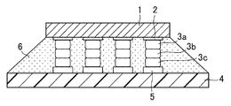
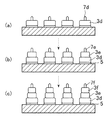
図1乃至図3は本発明の実施の形態1を示すものであり、図1は実施の形態1のフリップチップ実装方法により半導体素子が実装された回路基板の断面図、図2は、実施の形態1の3段バンプの形成過程を示す断面図、図3は実施の形態1のフリップチップ実装方法の工程を示す断面図である。
【0021】
図1に示すように、本実施の形態1により得られる電子機器は、半導体素子1、半導体素子1上の電極2、電極2上に形成された第1の金バンプ3a、第2の金バンプ3b、第3の金バンプ3c、回路基板4、回路基板4上の電極5、半導体素子1と回路基板4の間を接着固定した異方性導電接着剤6から構成されている。
【0022】
(作用)
図2(a)に示すように、3段バンプは、まず半導体素子1の電極2上に、ボールボンディング法により金属接合で第1の金バンプ3aを形成する。このボールボンディング法は、半導体素子1を組み立てる際に用いられるワイヤボンディング装置がペアチップの電極と外部に接続する電極との間にワイヤを形成するのに対して、基部を形成したところでワイヤを切断し、この基部(ボール)をバンプとして用いるものである。
【0023】
第1の金バンプ3aの先端には、引きちぎり痕7aが存在する。ここでは引きちぎり痕7aをそのままにしているが、場合によっては平面プレート(図示せず)を押し当て先端をレベリングしてもよい。
【0024】
次に、図2(b)に示すように、第1の金バンプ3a上に前記ボールボンディング法で第2の金バンプ3bを形成する。さらに、図2(c)に示すように、第2の金バンプ3b上に前記ボールボンデイング法で第3の金バンプ3cを形成する。
【0025】
ここで、図2(b)、(c)における7b及び7cは、前記引きちぎり痕7aと同様に金バンプ形成時に発生する引きちぎり痕である。ここでは、半導体素子1の電極2上に3段バンプを形成したが、回路基板4の電極5上に形成してもよい。
【0026】
図3(a)に示すように、3段バンプが形成された半導体素子を、回路基板4の電極5と相対するように位置合わせした後、異方性導電接着剤6を回路基板4上に塗布する。場合によっては、異方性導電接着剤6を回路基板4に塗布した後、位置合わせしてもよい。
【0027】
次に、図3(b)に示すように、半導体素子1の上面から熱と圧力を加え、金バンプ3cと電極5を接触し、3段バンプを塑性変形させた後、異方性導電接着剤6を硬化収縮させて、金バンプ3cと電極5との電気的接続をとる。こうして、フリップチップを実装した回路基板4を製造する。
【0028】
このように異方性導電接着剤6を塗布するに際して、特に電極5をよける必要もなく金バンプ3cと電極5を圧接すれば電気的接続が得られる。
【0029】
ここでは、3段バンプとしたが形成するバンプの段数を替えることにより半導体素子1と回路基板4との間の距離を調整できる。
【0030】
なお、異方性導電接着剤6に対して熱を効率的に伝えるために、回路基板4を加熱してもよい。
【0031】
(効果)
上述したフリップチップ実装方法によれば、バンプを溶融せずに接続しているので、バンプ間のブリッジが発生しない。また、金バンプ3a、3b、3cを同一形状にしているとともに、半導体素子1か又は回路基板4の一方にのみ金バンプ3a、3b、3cを形成することにより、バンプ製造工程が簡略で少工程数で済み、加工費を最小にできる利点がある。
【0032】
(実施の形態2)
(構成)
図4及び図5を参照して、本発明の実施の形態2を説明する。図4は、実施の形態2のフリップチップ実装方法により半導体素子1が実装された回路基板4を示す断面図である。図5は、実施の形態2の3段バンプの形成過程を示す断面図である。
【0033】
本実施の形態2は、実施の形態1と以下の点で異なる。即ち、図4に示すように、金バンプ3d、金バンプ3e、金バンプ3fの順にバンプ径が小さい3段バンプ構成としている。
【0034】
(作用)
図5(a)に示すように、本実施の形態2の3段バンプを形成するには、まず半導体素子1の電極2上に、バンプ径が最大の金バンプ3dを形成する。次に、図5(b)に示すように金バンプ3d上にバンプ径の小さい金バンプ3eを形成する。さらに、図5(c)に示すように金バンプ3e上にバンプ径が最小の金バンプ3fを形成し、3段バンプが完成する。これ以降の工程は実施の形態1の場合と同様である。
【0035】
(効果) 上述したフリップチップ実装方法によれば、実施の形態1の効果を発揮することに加えて、多段バンプ形成工程において、バンプ形成中心位置が多少ずれてもバンプ構造が不安定にならないのでバンプ倒れが発生しにくく、バンプ形成工程の歩留まりが高くなるという効果を奏する。
【0036】
(実施の形態3)
(構成)
図6を参照して、本発明の実施の形態3について説明する。図6は、本実施の形態3のフリップチップ実装方法の工程を示す断面図である。
【0037】
本実施の形態3は、異方性導電接着剤を用いていない点で実施の形態1の場合と異なり、これ以外の工程は実施の形態1と同様である。
【0038】
(作用)
図6(a)に示すように、半導体素子1の電極2上に金バンプ3a、3b、の2段ダンプを形成し、一方で回路基板4の電極5上に金バンプ3gを形成する。
【0039】
次に、図6(b)に示すように、2段バンプが形成された半導体素子1を、回路基板4の電極5と相対するように位置合わせした後、半導体素子1の上面から熱と圧力を加え、金バンプ3bと金バンプ3gを接触させ、金属接合させて金バンプ3bと金バンプ3gとの電気的接続をとる。こうしてフリップチップを実装した回路基板4を製造する。
【0040】
尚、金バンプ3bと金バンプ3gとの接合部の信頼性を向上させるためこれら金バンプ3bと金バンプ3gとを接続した後に半導体素子1と回路基板4との間に絶縁性接着剤を注入、硬化してもよい。
【0041】
(効果)
上述した本実施の形態3のフリップチップ実装方法によれば、実施の形態1の場合と同様な効果を発揮することに加えて、金バンプ3bと金バンプ3gとを接合する金−金接合のフリップッチップ実装方法であるため、金バンプと電極とを接触させる実施の形態1、2の実装方法に比べて、多段バンプを有する回路基板4を製造することが容易であるという利点がある。
【0042】
(実施の形態4)
(構成)
図7を参照して、本発明の実施の形態4について説明する。図7は、本実施の形態4のフリップチップ実装方法の工程を示す断面図である。
【0043】
本実施の形態4は、実施の形態3と比べ、回路基板4の電極5に形成した金バンプ3hと、この金バンプ3h上に形成した金バンプ3iを備え、金バンプ3iのバンプ径を金バンプ3hよりも小径とした点が異なるものである。
【0044】
(作用)
図7(a)に示すように、半導体素子1の電極2上に金バンプ3aを形成し、一方で回路基板4の電極5上に金バンプ3hを形成する。さらに、金バンプ3h上に複数の小径の金バンプ3iを形成する。
【0045】
次に、図7(b)に示すように、金バンプ3aが形成された半導体素子1を、回路基板4の電極5と相対するように位置合わせした後、半導体素子1の上面から熱と圧力を加え、金バンプ3aと小径の金バンプ3iとを引きちぎり痕7aが金バンプ3iの間の隙間に嵌合するようにして接触させ、かつ、金属接合させて金バンプ3aと金バンプ3iとの電気的接続をとる。こうしてフリップチップを実装した回路基板4を製造する。
【0046】
(効果)
本実施の形態4のフリップチップ実装方法によれば、実施の形態1乃至3の場合と同様な効果を発揮することに加え、金バンプ3aと金バンプ3iが嵌合する状態で接触しかつ金属接合するために、接合強度が強い金−金接合の多段バンプを備えた回路基板4を製造できるという効果も奏する。
【0047】
【発明の効果】
本発明によれば、フリップチップ実装を行う場合に、半導体素子と回路基板の間隔を大きくすることができ、かつ、実装強度を高めることができるとともに、実装時に多少の位置ずれが生じても接触不良になりにくく歩留まりの高いフリップチップ実装品を得ることができるフリップチップ実装方法を提供することができる。
【図面の簡単な説明】
【図1】本発明の実施の形態1のフリップチップ実装方法により半導体素子が実装された回路基板を示す断面図である。
【図2】実施の形態1の3段バンプの形成過程を示す断面図である。
【図3】実施の形態1のフリップチップ実装方法の工程を示す断面図である。
【図4】実施の形態2のフリップチップ実装方法により半導体素子が実装された回路基板を示す断面図である。
【図5】実施の形態2の3段バンプの形成過程を示す断面図である
【図6】実施の形態3のフリップチップ実装方法の工程を示す断面図である.
【図7】実施の形態4のフリップチップ実装方法の工程を示す断面図である。
【図8】従来のフリップチップ実装方法により半導体素子が実装された回路基板を示す断面図である。
【符号の説明】
1 半導体素子
2 電極
3a 金バンプ
3b 金バンプ
3c 金バンプ
3d 金バンプ
3e 金バンプ
3f 金バンプ
3g 金バンプ
3h 金バンプ
3i 金バンプ
4 回路基板
5 電極
6 異方性導電接着剤
7a 引きちぎり痕
7b 引きちぎり痕
7c 引きちぎり痕
7d 引きちぎり痕
7e 引きちぎり痕
7f 引きちぎり痕[0001]
BACKGROUND OF THE INVENTION
The present invention relates to a flip chip mounting method, and more particularly to a flip chip mounting method in which a semiconductor element and a circuit board are electrically connected using multi-stage bumps.
[0002]
[Prior art]
Conventionally, as a flip chip mounting method for mounting a semiconductor element on a circuit board, one disclosed in Japanese Patent Laid-Open No. 8-1786 is known.
[0003]
As shown in FIG. 8, a mounting form obtained by the flip chip mounting method disclosed in the publication includes a
[0004]
In such a flip-chip mounting method, the
[0005]
Thereafter, the
[0006]
In the conventional example shown in FIG. 8, when the
[0007]
[Problems to be solved by the invention]
However, in the case of the conventional example shown in FIG. 8, since (1) the solder bumps are melted by heat, there is a high risk of bridging between adjacent solder bumps, and it is difficult to form multi-stage bumps with a narrow bump pitch. It is. (2) An operation time for adhering and curing the
[0008]
The present invention has been made in view of the above circumstances, and an object of the present invention is to provide a flip chip mounting method capable of forming multi-stage bumps having a narrow bump pitch in a short time and efficiently mounting semiconductor elements on a circuit board. And
[0009]
[Means for Solving the Problems]
According to a first aspect of the present invention, in a flip chip mounting method in which a semiconductor element and a circuit board are electrically connected using bumps, a first gold bump is formed on an electrode of the circuit board. A plurality of second gold bumps having a bump diameter smaller than that of the gold bumps are formed on the first gold bumps so that a gap is formed therebetween, and a third gold bump is formed on the electrode of the semiconductor element. Forming and contacting a part of the third gold bump so as to fit into a gap between the plurality of second gold bumps, and mounting the semiconductor element on the circuit board. It is what.
[0010]
According to the present invention, in a flip-chip mounting method in which a semiconductor element and a circuit board are electrically connected using bumps, the bump diameter is the first gold bump on the first gold bump formed on the electrode of the circuit board. A plurality of smaller second gold bumps are formed so as to create a gap between them, a third gold bump is formed on the electrode of the semiconductor element, and a part of the third gold bump is placed on the plurality of second gold bumps. Since the contact is made so as to fit in the gap between the two gold bumps, the distance between the semiconductor element and the circuit board can be increased , the mounting strength can be increased , and a little during mounting. Even if the positional deviation occurs, it is possible to obtain a flip-chip mounted product that does not cause poor contact and has a high yield.
[0011]
A second aspect of the present invention is the flip chip mounting method according to the first aspect, wherein the gold bump is formed by a ball bonding method.
[0012]
According to the present invention, the same effect as that of the invention described in
[0019]
DETAILED DESCRIPTION OF THE INVENTION
Hereinafter, embodiments of the present invention will be described in detail. In the following first to fourth embodiments, an example in which a flip chip is mounted using a gold three-stage bump is described.
[0020]
(Embodiment 1)
(Constitution)
1 to 3 show a first embodiment of the present invention. FIG. 1 is a cross-sectional view of a circuit board on which a semiconductor element is mounted by the flip-chip mounting method of the first embodiment, and FIG. FIG. 3 is a cross-sectional view showing the steps of the flip-chip mounting method according to the first embodiment.
[0021]
As shown in FIG. 1, the electronic device obtained by the first embodiment includes a
[0022]
(Function)
As shown in FIG. 2A, in the three-step bump, first, a
[0023]
A
[0024]
Next, as shown in FIG. 2B, the
[0025]
Here, 7b and 7c in FIGS. 2 (b) and 2 (c) are tear marks generated at the time of gold bump formation, similar to the tear marks 7a. Here, the three-step bump is formed on the
[0026]
As shown in FIG. 3A, after the semiconductor element on which the three-step bumps are formed is aligned so as to face the
[0027]
Next, as shown in FIG. 3 (b), heat and pressure are applied from the upper surface of the
[0028]
Thus, when applying the anisotropic
[0029]
Although the three-stage bump is used here, the distance between the
[0030]
The
[0031]
(effect)
According to the flip chip mounting method described above, since the bumps are connected without melting, a bridge between the bumps does not occur. In addition, the gold bumps 3a, 3b, and 3c are formed in the same shape, and the bump manufacturing process is simplified and reduced by forming the gold bumps 3a, 3b, and 3c only on one of the
[0032]
(Embodiment 2)
(Constitution)
A second embodiment of the present invention will be described with reference to FIGS. FIG. 4 is a cross-sectional view showing the
[0033]
The second embodiment is different from the first embodiment in the following points. That is, as shown in FIG. 4, a three-step bump configuration is employed in which the bump diameter is smaller in the order of the
[0034]
(Function)
As shown in FIG. 5A, in order to form the three-step bump of the second embodiment, first, the
[0035]
(Effect) According to the flip chip mounting method described above, in addition to exhibiting the effects of the first embodiment, the bump structure does not become unstable even if the bump formation center position is slightly shifted in the multi-stage bump formation process. Bump collapse is unlikely to occur, and the yield of the bump forming process is increased.
[0036]
(Embodiment 3)
(Constitution)
A third embodiment of the present invention will be described with reference to FIG. FIG. 6 is a cross-sectional view showing the steps of the flip chip mounting method of the third embodiment.
[0037]
The third embodiment is different from the first embodiment in that an anisotropic conductive adhesive is not used, and the other steps are the same as those in the first embodiment.
[0038]
(Function)
As shown in FIG. 6A, a two-stage dump of
[0039]
Next, as shown in FIG. 6B, the
[0040]
In order to improve the reliability of the joint between the
[0041]
(effect)
According to the flip-chip mounting method of the third embodiment described above, in addition to exhibiting the same effect as that of the first embodiment, the gold-gold bonding for bonding the
[0042]
(Embodiment 4)
(Constitution)
A fourth embodiment of the present invention will be described with reference to FIG. FIG. 7 is a cross-sectional view showing the steps of the flip chip mounting method according to the fourth embodiment.
[0043]
Compared with the third embodiment, the fourth embodiment includes a
[0044]
(Function)
As shown in FIG. 7A, gold bumps 3 a are formed on the
[0045]
Next, as shown in FIG. 7B, the
[0046]
(effect)
According to the flip chip mounting method of the fourth embodiment, in addition to exhibiting the same effects as those of the first to third embodiments, the
[0047]
【The invention's effect】
According to the present invention, when flip chip mounting is performed, the distance between the semiconductor element and the circuit board can be increased, and the mounting strength can be increased. It is possible to provide a flip chip mounting method capable of obtaining a flip chip mounting product which is less likely to become defective and has a high yield .
[Brief description of the drawings]
FIG. 1 is a cross-sectional view showing a circuit board on which a semiconductor element is mounted by a flip chip mounting method according to a first embodiment of the present invention.
FIG. 2 is a cross-sectional view showing a process of forming a three-step bump according to the first embodiment.
FIG. 3 is a cross-sectional view showing a process of the flip chip mounting method of the first embodiment.
4 is a cross-sectional view showing a circuit board on which a semiconductor element is mounted by the flip-chip mounting method of
5 is a cross-sectional view showing a process of forming a three-step bump according to the second embodiment. FIG. 6 is a cross-sectional view showing a process of the flip chip mounting method according to the third embodiment.
7 is a cross-sectional view showing a process of the flip chip mounting method of
FIG. 8 is a cross-sectional view showing a circuit board on which a semiconductor element is mounted by a conventional flip chip mounting method.
[Explanation of symbols]
DESCRIPTION OF
Claims (2)
前記回路基板の電極上に第1の金バンプを形成し、
この第1の金バンプよりバンプ径が小さい複数の第2の金バンプを、その間に隙間が生じるようにして前記第1の金バンプ上に形成し、
前記半導体素子の電極上に、第3の金バンプを形成し、
この第3の金バンプの一部が、前記複数の第2の金バンプの間の隙間に嵌合するようにして接触させ、前記回路基板上に前記半導体素子を実装することを特徴とするフリップチップ実装方法。In a flip chip mounting method in which a semiconductor element and a circuit board are electrically connected using bumps,
Forming a first gold bump on the electrode of the circuit board;
A plurality of second gold bumps having a smaller bump diameter than the first gold bumps are formed on the first gold bumps so that gaps are formed therebetween,
Forming a third gold bump on the electrode of the semiconductor element;
Flip characterized in that a part of the third gold bump is brought into contact with a gap between the plurality of second gold bumps and the semiconductor element is mounted on the circuit board. Chip mounting method.
Priority Applications (1)
| Application Number | Priority Date | Filing Date | Title |
|---|---|---|---|
| JP2002075863A JP3746719B2 (en) | 2002-03-19 | 2002-03-19 | Flip chip mounting method |
Applications Claiming Priority (1)
| Application Number | Priority Date | Filing Date | Title |
|---|---|---|---|
| JP2002075863A JP3746719B2 (en) | 2002-03-19 | 2002-03-19 | Flip chip mounting method |
Publications (3)
| Publication Number | Publication Date |
|---|---|
| JP2003273148A JP2003273148A (en) | 2003-09-26 |
| JP2003273148A5 JP2003273148A5 (en) | 2005-06-02 |
| JP3746719B2 true JP3746719B2 (en) | 2006-02-15 |
Family
ID=29204824
Family Applications (1)
| Application Number | Title | Priority Date | Filing Date |
|---|---|---|---|
| JP2002075863A Expired - Fee Related JP3746719B2 (en) | 2002-03-19 | 2002-03-19 | Flip chip mounting method |
Country Status (1)
| Country | Link |
|---|---|
| JP (1) | JP3746719B2 (en) |
Cited By (1)
| Publication number | Priority date | Publication date | Assignee | Title |
|---|---|---|---|---|
| US10354967B2 (en) | 2016-09-29 | 2019-07-16 | Samsung Electronics Co., Ltd. | Metal pillar in a film-type semiconductor package |
Families Citing this family (2)
| Publication number | Priority date | Publication date | Assignee | Title |
|---|---|---|---|---|
| JP2006318974A (en) * | 2005-05-10 | 2006-11-24 | Toshiba Components Co Ltd | Semiconductor device using bump structure and its manufacturing method |
| WO2019150825A1 (en) * | 2018-02-01 | 2019-08-08 | パナソニックIpマネジメント株式会社 | Semiconductor device |
-
2002
- 2002-03-19 JP JP2002075863A patent/JP3746719B2/en not_active Expired - Fee Related
Cited By (2)
| Publication number | Priority date | Publication date | Assignee | Title |
|---|---|---|---|---|
| US10354967B2 (en) | 2016-09-29 | 2019-07-16 | Samsung Electronics Co., Ltd. | Metal pillar in a film-type semiconductor package |
| US10867948B2 (en) | 2016-09-29 | 2020-12-15 | Samsung Electronics Co., Ltd. | Metal pillar in a film-type seconductor package |
Also Published As
| Publication number | Publication date |
|---|---|
| JP2003273148A (en) | 2003-09-26 |
Similar Documents
| Publication | Publication Date | Title |
|---|---|---|
| JP4729963B2 (en) | PROJECT ELECTRODE FOR CONNECTING ELECTRONIC COMPONENT, ELECTRONIC COMPONENT MOUNTING BODY USING SAME, AND METHOD FOR PRODUCING THEM | |
| JP5421863B2 (en) | Manufacturing method of semiconductor package | |
| JP5066935B2 (en) | Method for manufacturing electronic component and electronic device | |
| JP2001176918A (en) | Tape carrier-type semiconductor device, its manufacturing method and liquid crystal module using the same | |
| TWI539586B (en) | Flip chip bonding method, and method for manufacturing solid-state imaging device including the flip chip bonding method | |
| JP3308855B2 (en) | Method for manufacturing semiconductor device | |
| JP3243956B2 (en) | Semiconductor device and manufacturing method thereof | |
| JP3746719B2 (en) | Flip chip mounting method | |
| JP2001351945A (en) | Method of manufacturing semiconductor device | |
| JPH10270497A (en) | Semiconductor element fixing method | |
| JP4934831B2 (en) | Manufacturing method of semiconductor package | |
| JP2001267366A (en) | Method of packaging semiconductor and printed circuit board | |
| JPH11111755A (en) | Manufacture of semiconductor device | |
| JP2005353854A (en) | Wiring board and semiconductor device using the same | |
| JPH11326935A (en) | Anisotropic conductive film and its connection method | |
| JP2001210676A (en) | Semiconductor device and manufacturing method | |
| JP2002016104A (en) | Mounting method of semiconductor device and manufacturing method of semiconductor device mounted assembly | |
| JP4520052B2 (en) | Semiconductor device and manufacturing method thereof | |
| JP2005183561A (en) | Method for manufacturing semiconductor device | |
| JPH09246273A (en) | Bump structure | |
| JP2003243447A (en) | Method of mounting semiconductor element | |
| JP2002313840A (en) | Semiconductor element board mounting and its manufacturing method | |
| JP3674550B2 (en) | Semiconductor device | |
| JP2009070930A (en) | Semiconductor device and its manufacturing method | |
| JP2001351948A (en) | Circuit board for mounting semiconductor chip, and method for mounting the semiconductor chip thereon |
Legal Events
| Date | Code | Title | Description |
|---|---|---|---|
| A521 | Written amendment |
Free format text: JAPANESE INTERMEDIATE CODE: A523 Effective date: 20040819 |
|
| A621 | Written request for application examination |
Free format text: JAPANESE INTERMEDIATE CODE: A621 Effective date: 20040819 |
|
| A977 | Report on retrieval |
Free format text: JAPANESE INTERMEDIATE CODE: A971007 Effective date: 20050323 |
|
| A131 | Notification of reasons for refusal |
Free format text: JAPANESE INTERMEDIATE CODE: A131 Effective date: 20050329 |
|
| A521 | Written amendment |
Free format text: JAPANESE INTERMEDIATE CODE: A523 Effective date: 20050525 |
|
| TRDD | Decision of grant or rejection written | ||
| A01 | Written decision to grant a patent or to grant a registration (utility model) |
Free format text: JAPANESE INTERMEDIATE CODE: A01 Effective date: 20051115 |
|
| A61 | First payment of annual fees (during grant procedure) |
Free format text: JAPANESE INTERMEDIATE CODE: A61 Effective date: 20051124 |
|
| R151 | Written notification of patent or utility model registration |
Ref document number: 3746719 Country of ref document: JP Free format text: JAPANESE INTERMEDIATE CODE: R151 |
|
| FPAY | Renewal fee payment (event date is renewal date of database) |
Free format text: PAYMENT UNTIL: 20081202 Year of fee payment: 3 |
|
| FPAY | Renewal fee payment (event date is renewal date of database) |
Free format text: PAYMENT UNTIL: 20091202 Year of fee payment: 4 |
|
| FPAY | Renewal fee payment (event date is renewal date of database) |
Free format text: PAYMENT UNTIL: 20101202 Year of fee payment: 5 |
|
| FPAY | Renewal fee payment (event date is renewal date of database) |
Free format text: PAYMENT UNTIL: 20111202 Year of fee payment: 6 |
|
| FPAY | Renewal fee payment (event date is renewal date of database) |
Free format text: PAYMENT UNTIL: 20111202 Year of fee payment: 6 |
|
| FPAY | Renewal fee payment (event date is renewal date of database) |
Free format text: PAYMENT UNTIL: 20121202 Year of fee payment: 7 |
|
| FPAY | Renewal fee payment (event date is renewal date of database) |
Free format text: PAYMENT UNTIL: 20131202 Year of fee payment: 8 |
|
| S531 | Written request for registration of change of domicile |
Free format text: JAPANESE INTERMEDIATE CODE: R313531 |
|
| R350 | Written notification of registration of transfer |
Free format text: JAPANESE INTERMEDIATE CODE: R350 |
|
| R250 | Receipt of annual fees |
Free format text: JAPANESE INTERMEDIATE CODE: R250 |
|
| LAPS | Cancellation because of no payment of annual fees |