JP3720552B2 - Dual clock synchronous control system - Google Patents
Dual clock synchronous control system Download PDFInfo
- Publication number
- JP3720552B2 JP3720552B2 JP30523997A JP30523997A JP3720552B2 JP 3720552 B2 JP3720552 B2 JP 3720552B2 JP 30523997 A JP30523997 A JP 30523997A JP 30523997 A JP30523997 A JP 30523997A JP 3720552 B2 JP3720552 B2 JP 3720552B2
- Authority
- JP
- Japan
- Prior art keywords
- phase
- reference timing
- timing generation
- synchronization
- block
- Prior art date
- Legal status (The legal status is an assumption and is not a legal conclusion. Google has not performed a legal analysis and makes no representation as to the accuracy of the status listed.)
- Expired - Fee Related
Links
Images


Landscapes
- Detection And Prevention Of Errors In Transmission (AREA)
- Synchronisation In Digital Transmission Systems (AREA)
Description
【0001】
【発明の属する技術分野】
本発明は二重化クロックの同期制御システムに関し、更に詳しくはクロック源間の同期制御及びこのクロックを使用する機能ブロックのクロック同期制御に関する。
【0002】
【従来の技術】
図7は従来システムの構成例を示すブロック図である。このシステムは、装置基準タイミング生成ブロックを100aと100bに二重化し、このブロックが出力する基準タイミングの同期を図ると共に、このタイミングを使用する機能ブロック200間の同期化を図るものである。200は機能ブロック基準タイミング生成ブロックであり、複数設けられている。
【0003】
二重化された装置基準タイミング生成ブロック100a、100b間の同期制御は、運用系が予備系の同期制御基準カウンタ103のロード位相調整により基準タイミングの位相調整を行なって、基準タイミングの同期を図っている。
【0004】
運用系/予備系の設定は、それぞれの系選択制御部101にて一方が運用系、他方が予備系となるように系選択を行なっている。系選択要因としては、例えば自系の異常監視部110での異常検出、他系の系選択制御部101から与えられる接続情報、異常検出信号及び装置制御ブロック300から出力される系切り替え指示信号等がある。
【0005】
同期制御基準カウンタ103は、装置基準タイミング生成ブロック100a又は100b内の基準となるタイミング信号を生成する。この同期制御基準カウンタ103のロード信号は、2−1セレクタ102により運用系設定時は同期制御基準カウンタ103が出力したタイミング信号、予備系設定時は運用系の同期信号生成部106が出力する装置基準タイミング生成ブロック同期信号を選択する。
【0006】
装置基準タイミング生成部107及び並走クロック生成部108は、同期制御基準カウンタ103が出力するタイミング信号を基に機能ブロック基準タイミングブロック200に供給する装置基準タイミングクロックと並走クロックを生成する。
【0007】
同期信号入力位相監視部104は、運用系設定時に他系である予備系の装置基準タイミング生成ブロックの同期信号生成部106より受け取る同期信号と、自系の同期制御基準カウンタ103が出力した同期信号を比較し、運用系と予備系の基準タイミングの位相差を算出し、位相調整部105へ送る。
【0008】
位相調整部105は、同期信号入力位相監視部104が検出した位相差量と同期制御基準カウンタ103が出力した基準信号を基に、同期信号生成部106が持つカウンタのロードタイミングを決定し、通知する。同期信号生成部106は、運用系設定時は位相調整部105が出力するロード信号を選択し、予備系設定時は同期制御基準カウンタ103が出力した基準信号をロード信号として選択し、予備系へ渡す同期信号の生成を行なう。PLO(位相同期発振器)109は、自系ブロック内にて使用するクロックを生成する。異常監視部110は、ブロック内の異常検出結果を装置制御ブロック300へ通知する。
【0009】
装置内基準タイミング生成ブロック100a、100bと、機能ブロック基準タイミング生成ブロック200間の同期は、装置内基準タイミング生成ブロック100a、100bが出力した装置基準タイミングクロック及び並走クロックを使用し、機能ブロック基準タイミング生成ブロック200にて基準となる同期クロックを生成し、同期を図っている。系選択制御部201は、装置制御ブロック300より入力される切り替え指示に従い運用系/予備系切り替えを行なう。
【0010】
セレクタ202、203は、系選択制御部201より入力される切り替え指示に従い、運用系の0/1系切り替えを行なう。PLO204は、装置基準タイミング生成ブロック100a、100bより入力される運用系の並走クロックを使用して同期クロックを再生する。例えば、5MHzを184MHzに変換する。
【0011】
同期クロック生成基準カウンタ205は、PLO204にて再生された同期クロックと、装置基準タイミング生成ブロック100a、100bより入力される運用系の装置基準タイミングにてカウンタ205へロードを行ない、同期クロック生成基準信号を生成する。
【0012】
クロック生成部206は、同期クロック生成基準カウンタ205が出力するタイミング信号とPLO204が出力するクロックを基に論理ブロック400にて必要なタイミング信号及びクロックを生成する。装置制御ブロック300は、装置内で検出された異常や、外部から入力される切り替え指示により、装置基準タイミング生成ブロック100a、100b及び機能ブロック基準タイミング生成部200の系選択制御を行なう。
【0013】
図8は装置基準タイミング生成ブロック間(100aと100b間)同期を示すタイムチャートである。(a)は同期制御基準カウンタ103が出力する基準信号で、この信号を基に同期信号入力位相監視部104にて(b)の位相監視ウィンドウを生成する。この例では、ウィンドウは1〜7の7個のクロックから構成されている。以下、位相監視ウィンドウを±3クロックとした場合について説明する。
【0014】
運用系設定の場合、予備系の同期信号生成部106より入力される同期信号が(b)の位相監視ウィンドウの中心である“4”の位相に入力されるように位相調整部105が同期信号生成部106の調整を行なう。
【0015】
図9は従来の装置基準タイミング生成ブロック100aと100b間の同期制御を示すタイムチャートである。(a)と(b)は図8と同じであり、(a)は同期制御基準カウンタ103が出力する基準信号、(b)は同期信号入力位相監視部104にて作成されるウィンドウである。(c)は運用系同期信号生成部106が予備系へ出力する同期信号で、(d)は予備系の同期信号生成部06から運用系へ入力される同期信号である。運用系が出力した同期信号が、次の周期の2クロック早い位相に入力される場合を示す。
【0016】
位相(A)は立ち上げ時の動作で、運用系は基準位相“4”、予備系は同期制御基準カウンタ103へロード信号未入力のため信号未出力である。位相(B)では、前位相時に予備系からの信号が未入力であったために、再度運用系は基準位相“4”を出力し、予備系からは前位相にして運用系が出力した基準位相より2クロック早い位相“2”を受信する。
【0017】
位相(C)では、前位相にて運用系が位相“2”を受けたため、運用系は2クロック位相調整を行なった位相“6”を出力する。予備系からは、前位相にて運用系が出力した基準位相より2クロック早い位相“2”を受信する。
【0018】
位相(D)では、前位相にて運用系が位相“2”を受けたため、運用系は2クロック位相調整を行なった位相“6”を出力する。予備系からは、前位相にて運用系が出力した基準位相よりも2クロック早い位相“4”を受信する。位相(E)では、前位相にて運用系が位相“4”を受けたため同期が確立し、前位相と同位相“6”を出力する。以降、同期状態となる。
【0019】
図10は従来の装置基準タイミング生成ブロック間の他の動作を示すタイムチャートである。図9と同様に運用系が出力した同期信号が次の同期の2クロック早い位相に入力される場合であるが、この例は、同期状態時に予備系からの入力が位相(B)時に、クロックジッタ等により一度のみ1クロック遅く(通常より1クロック遅れて)入力された場合の動作を示している。位相(A)は正常であった為、位相(B)で運用系は位相“6”を出力し、次の位相(C)では位相“4”が入力される為、誤った出力位相“3”が保持される。以降、これをきっかけに同期制御を行っても位相が同期状態に収束せずに、つまり、信号(d)が“4”に固定されず同期ウィンドウ内で位相が発振して(同期はずれ)しまっている。
【0020】
【発明が解決しようとする課題】
前述した図7に示す従来の伝送及び交換機の二重化クロック同期制御法式では、系切り替え指示を装置制御ブロック300で実施している。このブロックが、装置全体の監視を行なうため、各ブロックを順に監視を行なった後に制御を実施するため、切り替え制御の実施に時間を有する。
【0021】
また、図7に示す従来の伝送及び交換機の二重化クロック同期制御法式では、機能ブロック基準タイミング生成ブロック200の運用系切り替えを、装置制御ブロック300の切り替え指示に従い実施する。装置基準タイミング生成ブロック100a、100bが出力するタイミング信号の異常検出は、タイミング生成ブロック以外で実施しているため、検出及び異常の通知に時間がかかり、異常からの復旧に時間を要してしまう。また、運用系の0/1系切り替えは、機能ブロック基準タイミング生成ブロック200に同期監視機能を持たないため、無瞬断切り替えが可能か否かの判断機能を持たなかった。
【0022】
本発明はこのような課題に鑑みてなされたものであって、装置の保守が容易で、かつクロック異常時に自動切り替えを可能とすると共に、あらゆる周波数に対して対応することができる二重化クロックの同期制御システムを提供することを目的としている。
【0023】
【課題を解決するための手段】
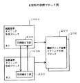
(1)図1は本発明の原理ブロック図である。図7と同一のものは、同一の符号を付して示す。図において、100aと100bは二重化された装置基準タイミング生成ブロック、200はこれら装置基準タイミング生成ブロック100a又は100bの運用系から基準クロックを受ける機能ブロック基準タイミング生成ブロックである。400は前記各装置基準タイミング生成ブロック100a又は10bの何れかが運用系となった時に、他方の予備系に対して位相修正を行なう際に、位相修正周期と位相保持周期を交互に発生する位相修正手段である。
【0024】
この発明の構成によれば、装置基準タイミング生成ブロック100a、100bの運用系の同期制御基準カウンタが出力する基準信号と、予備系の同期信号生成部が出力する同期信号の位相差を同期信号入力位相監視部にて検出し、位相調整部へ通知する。位相調整部は、現在実施している位相調整に対し、同期生成部にて検出された位相差分の調整を行なう。但し、位相調整の修正を行なう周期は毎周期とせず1周期以上毎に行なうことで、同期状態へ収束させることが可能となる。
【0025】
この発明の構成によれば、位相修正手段が位相修正周期と位相保持周期を交互に繰り返すことにより、該位相修正手段が予備系の基準タイミングを期待する位相へ近づけるように動作することができる。
【0026】
(2)この場合において、二重化された装置基準タイミング生成ブロックの同期制御において、同期が外れた場合、運用系が予備系に対して位相修正を行なう際に、前記位相修正手段は、徐々に予備系の基準タイミングを期待する位相へ近づけていくことを特徴としている。
【0027】
この発明の構成によれば、位相差の監視方法をプラスかマイナスかの判断のみとし、±1クロックずつ同期確立まで1周期以上毎に調整を行なうことで、同期状態へ収束させると共に、制御の単純化が図れるため、回路規模の削減が可能となる。
【0028】
(3)また、二重化された装置基準タイミング生成ブロックの運用系/予備系の切り替えにおいて、基準タイミング信号の分配先に分配信号の監視手段を設け、この監視手段にて異常検出部はアラームを系選択制御部に通知し、運用系を自動的に切り替えることを特徴としている。
【0029】
この発明の構成によれば、機能ブロック基準タイミング生成ブロック200に0/1系別に装置基準タイミング生成ブロック100a、100bが出力する信号の監視部を設け、直接装置基準タイミング生成ブロック100a、100bの系選択制御部にアラームを通知することで、異常発生時の切り替え制御の高速化を図ることができる。
【0040】
【発明の実施の形態】
以下、図面を参照して本発明の実施の形態例を詳細に説明する。
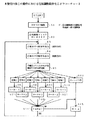
図2は本発明の一実施の形態例を示す構成ブロック図である。図7と同一のものは、同一の符号を付して示す。図において、207aは装置基準タイミング生成ブロック100aの装置基準タイミング生成部107と並走クロック生成部108の出力を受けて異常を監視する0系異常監視部、207bは装置基準タイミング生成ブロック100bの装置基準タイミング生成部107と並走クロック生成部108の出力を受けて異常を監視する1系異常監視部である。201は、装置基準タイミング生成ブロック100aと100bの異常監視部110からの信号と装置制御ブロック300の出力を受けて系選択制御を行なう系選択制御部である。その他の構成は、図7と同じである。このように構成されたシステムの動作を説明すれば、以下の通りである。
【0041】
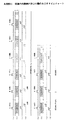
図3は本発明の一実施の形態例の第1の動作を示すタイムチャートである。(a)は同期制御基準カウンタ103が出力する基準信号で、この信号を基に同期信号入力位相監視部104にて(b)の位相監視ウィンドウを生成する。(c)は運用系同期信号生成部106が予備系へ出力する同期信号で、(d)は予備系から運用系へ入力される同期信号である。
【0042】
運用設定された装置基準タイミング生成ブロック100a、100bの同期信号入力位相監視部104は、同期制御基準カウンタ103が出力する信号(a)より同期監視ウィンドウ(b)を生成する。この信号と他系の同期信号生成部106より入力される同期信号(d)の位相差を位相調整部105へ通知する。この信号を基に、位相調整部105は、同期信号生成部106の位相調整を行なう。
【0043】
位相調整は2周期に1回とし、位相調整を行なう場合は同期ウィンドウの中心“4”と、入力同期信号(d)の位相差を現在の位相調整部105が行なっている位相調整量に対し±Nクロックの調整を行なう。位相調整を行なった次の周期は前位相と同位相調整のままとする。つまり、前の状態を保持する。なお、装置立ち上げ時及び他系より入力される同期信号(d)が監視ウィンドウから外れていた場合は、ウィンドウの中心位相“4”を同期信号として次周期に出力する。
【0044】
図3を用いて同期の様子を説明する。図3は本発明の一実施の形態例の第1の動作を示すタイムチャートである。このタイムチャートは、運用系が2クロック早く戻る場合の同期制御で、位相(B)に1度だけ通常より1クロック遅れて入力される場合を示す。位相(A)は、位相保持周期で同期中である。次に、位相(B)で予備系より同期信号が1周期遅れて入力されたため、同期外れが発生している。位相“5”に入力されたため、現在の調整量である+2(位相“6”)に対して−1クロックの位相(位相“5”)を次の位相(C)で出力する。
【0045】
位相(C)は、位相保持周期のため、次の周期(D)も位相“5”を出力する。位相(D)は制御周期で位相“3”が予備系から入力されたため、現在の位相調整量である+2(位相“5”)に対し+1(位相“6”)を次の周期に出力する。位相(E)は保持位相のため、次の周期(F)も“6”を出力する。位相(F)は制御周期であるが、同期したため、出力位相“6”を保持する。以上より、予備系制御を同期へ収束させることが可能となる。
【0046】
図4は本発明の第1の動作における位相調整動作を示すフローチャートである。先ずリセットして初期化する(S1)。これにより、位相調整のデフォルト値がN=4にセットされる(S2)。ここで、Nは位相調整部105が同期信号生成部106に渡す調整値である。
【0047】
次に、位相Nで同期信号を出力する(S3)。この時は、保持位相である。次に、位相Nで同期信号を出力する(S4)。この時には、制御位相である。この結果、予備系から同期信号が返ってくる。予備系より入力された同期信号の位相の比較を行なう(S5)。
【0048】
予備系より入力される同期信号の位相が1である時(基準に対し位相差−3)には、N=N+3とし(S6)、入力位相が2である時(位相差−2)にはN=N+2とし(S7)、入力位相が3である時(位相差−1)にはN=N+1とし(S8)、入力位相が4である時(位相差なし)にはN=Nとし(S9)、入力位相が5である時(位相差+1)にはN=N−1とし(S10)、入力位相が6である時(位相差+2)にはN=N−2とし(S11)、入力位相が7である時(位相差+3)にはN=N−3とする(S12)。入力位相がそれ以上(±3以上)あり、ウィンドウ外である時には(S13)、N=4の初期値に戻す(S15)。ステップS6〜ステップS12までの処理が終了したら、1≦N≦7であるかどうかチェックする(S14)。そうである時にはステップS3に戻って、位相調整制御を行ない、そうでない時にはステップS15でN=4に初期化する。このような一連の動作により予備系からの同期信号を運用系の同期信号に同期化することができる。
【0049】
この実施の形態例によれば、位相修正手段が位相修正周期と位相保持周期を交互に繰り返すことにより、該位相修正手段が予備系の基準タイミングを期待する位相へ近づけるように動作することができる。
【0050】
図5は本発明の一実施の形態例の第2の動作を示すタイムチャートである。運用系設定された装置基準タイミング生成ブロック100a、100bの同期信号入力位相監視部104は、同期制御基準カウンタ103が出力する信号(a)より同期監視ウィンドウ(b)を生成する。この信号と、他系の同期信号生成部106より入力される同期信号(d)の位相差がプラスかマイナスかを位相調整部105に通知する。
【0051】
この信号を基に位相調整部105は、同期信号生成部106に±1クロックの位相調整を行なう。第1の動作の場合は±3クロックである点で第2の動作と異なる。位相調整は2周期に1回とする。位相調整を行なった次の周期は前位相と同位相調整のままとする。なお、装置立ち上げ時及び他系より入力される同期信号が監視ウィンドウから外れていた場合には、ウィンドウの中心位相“4”を同期信号として次の周期に出力する。
【0052】
図5は2周期異常が発生した場合の同期へ向かうタイムチャートである。位相(A)は保持位相のため、位相(B)は出力位相を保持する。位相(B)は、予備系より位相“5”(+1位相)に入力されているため、次の周期にてマイナス調整を行なう。以降、同期確立まで位相調整を実施する。最終的には、図5に示すように、予備系からの同期信号(d)は位相“4”となり、運用系の位相に同期する。
【0053】
図6は本発明の第2の動作における位相調整動作を示すフローチャートである。先ずリセットして初期化する(S1)。これにより、位相調整のデフォルト値がN=4にセットされる(S2)。ここで、Nは位相調整部105が同期信号生成部106に渡す調整値である。
【0054】
次に、位相Nで同期信号を出力する(S3)。この時は、保持位相である。次に、位相Nで同期信号を出力する(S4)。この時には、制御位相である。この結果、予備系から同期信号が返ってくる。予備系より入力された同期信号の位相の比較を行なう(S5)。
【0055】
予備系からの同期信号入力位相が1である時には、N=N+1とし(S6)、入力位相が2である時にはN=N+1とし(S7)、入力位相が3である時にはN=N+1とし(S8)、入力位相が4である時にはN=Nとし(S9)、入力位相が5である時にはN=N−1とし(S10)、入力位相が6である時にはN=N−1とし(S11)、入力位相が7である時にはN=N−1とする(S12)。入力位相がそれ以上あり、ウィンドウ外である時には(S13)、N=4の初期値に戻す(S15)。ステップS6〜ステップS12までの処理が終了したら、1≦N≦7であるかどうかチェックする(S14)。そうである時にはステップS3に戻って、位相調整制御を行ない、そうでない時にはステップS15でN=4に初期化する。このような一連の動作により予備系からの同期信号を運用系の同期信号に同期化することができる。
【0056】
この実施の形態例によれば、位相差の監視方法をプラスかマイナスかの判断のみとし、±1クロックずつ同期確立まで1周期以上毎に調整を行なうことで、同期状態へ収束させると共に、制御の単純化が図れるため、回路規模の削減が可能となる。
【0057】
次に、図2を用いて第3の動作について説明する。機能ブロック基準タイミング生成ブロック200に0/1系別に装置基準タイミング生成部107が生成した装置基準タイミングクロックと、並走クロック生成部108が生成した並走クロックの異常監視部207a、207bを設ける。この監視部は、検出した異常を装置制御ブロック300と該当する系の装置基準タイミング生成ブロック100a、100bの系選択制御部101へ通知する。
【0058】
運用系の装置基準タイミング生成ブロック100a、100bの場合、通知を受けた系選択制御部101は、他系が接続されていると共に異常が検出されていないかを確認し、予備系へ切り替える。予備系の系選択制御部101は、他系より異常信号が入力されるため、予備系から運用系へ切り替えを行なう。以上のように、ハードウェアが直接系切り替えを行なうため、高速切り替えが可能となる。
【0059】
この実施の形態例によれば、機能ブロック基準タイミング生成ブロック200に0/1系別に装置基準タイミング生成ブロック100a、100bが出力する信号の監視部を設け、直接装置基準タイミング生成ブロック100a、100bの系選択制御部101にアラームを通知することで、異常発生時の切り替え制御の高速化を図ることができる。
【0084】
このように、本発明によれば、装置の保守が容易で、かつクロック異常時に自動切り替えを可能とすると共に、あらゆる周波数に対して対応することができる二重化クロックの同期制御システムを提供することができる。
【0085】
【発明の効果】
以上、詳細に説明したように、本発明によれば、
(1)二重化された装置基準タイミング生成ブロックと、これら装置基準タイミング生成ブロックの運用系から基準クロックを受ける機能ブロック基準タイミング生成ブロックとを具備するシステムにおいて、前記各装置基準タイミング生成ブロックのそれぞれが運用系となった時に、他方の予備系に対して位相修正を行なう際に、位相修正周期と位相保持周期を交互に発生する位相修正手段を具備し、該位相修正手段が予備系の基準タイミングを期待する位相へ近づけるように動作することにより、
位相修正手段が位相修正周期と位相保持周期を交互に繰り返して、該位相修正手段が予備系の基準タイミングを期待する位相へ近づけるように動作することができる。
【0086】
(2)この場合において、二重化された装置基準タイミング生成ブロックの同期制御において、同期が外れた場合、運用系が予備系に対して位相修正を行なう際に、前記位相修正手段は、徐々に予備系の基準タイミングを期待する位相へ近づけていくことにより、
位相差の監視方法をプラスかマイナスかの判断のみとし、±1クロックずつ同期確立まで1周期以上毎に調整を行なうことで、同期状態へ収束させると共に、制御の単純化が図れるため、回路規模の削減が可能となる。
【0087】
(3)また、二重化された装置基準タイミング生成ブロックの運用系/予備系の切り替えにおいて、基準タイミング信号の分配先に分配信号の監視手段を設け、この監視手段にて異常検出部はアラームを系選択制御部に通知し、運用系を自動的に切り替えることにより、
機能ブロック基準タイミング生成ブロックに0/1系別に装置基準タイミング生成ブロックが出力する信号の監視部を設け、直接装置基準タイミング生成ブロックの系選択制御部にアラームを通知することで、異常発生時の切り替え制御の高速化を図ることができる。
【0093】
このように、本発明によれば、装置の保守が容易で、かつクロック異常時に自動切り替えを可能とすると共に、あらゆる周波数に対して対応することができる二重化クロックの同期制御システムを提供することができる。
【図面の簡単な説明】
【図1】 本発明の原理ブロック図である。
【図2】 本発明の一実施の形態例を示すブロック図である。
【図3】 本発明の一実施の形態例の第1の動作を示すタイムチャートである。
【図4】 本発明の第1の動作における位相調整動作を示すフローチャートである。
【図5】 本発明の一実施の形態例の第2の動作を示すタイムチャートである。
【図6】 本発明の第2の動作における位相調整動作を示すタイムチャートである。
【図7】 従来システムの構成例を示すブロック図である。
【図8】 装置基準タイミング生成ブロック間同期を示すタイムチャートである。
【図9】 従来の装置基準タイミング生成ブロック間の動作を示すタイムチャートである。
【図10】 従来の装置基準タイミング生成ブロック間の他の動作を示すタイムチャートである。
【符号の説明】
100a 装置基準タイミング生成ブロック
100b 装置基準タイミング生成ブロック
200 機能ブロック基準タイミング生成ブロック
400 位相修正手段[0001]
BACKGROUND OF THE INVENTION
The present invention relates to a dual clock synchronization control system, and more particularly to a clock synchronization control between clock sources and a functional block using this clock.
[0002]
[Prior art]
FIG. 7 is a block diagram showing a configuration example of a conventional system. In this system, the apparatus reference timing generation block is duplicated into 100a and 100b, the reference timing output by this block is synchronized, and the
[0003]
In the synchronization control between the duplicated apparatus reference timing generation blocks 100a and 100b, the operation system adjusts the reference timing by adjusting the load phase of the standby synchronization
[0004]
In the setting of the active system / standby system, the system
[0005]
The synchronization
[0006]
The device
[0007]
The synchronization signal input
[0008]
The
[0009]
The synchronization between the in-device reference timing generation blocks 100a and 100b and the functional block reference
[0010]
The
[0011]
The synchronous clock
[0012]
The
[0013]
FIG. 8 is a time chart showing synchronization between the apparatus reference timing generation blocks (between 100a and 100b). (A) is a reference signal output from the synchronization
[0014]
In the case of the operational system setting, the
[0015]
FIG. 9 is a time chart showing the synchronization control between the conventional apparatus reference timing generation blocks 100a and 100b. (A) and (b) are the same as FIG. 8 , (a) is a reference signal output from the synchronization
[0016]
Phase (A) is an operation at the time of start-up, the operation system has a reference phase “4”, and the standby system has no signal since it is not input to the synchronous
[0017]
In the phase (C), since the operation system has received the phase “2” in the previous phase, the operation system outputs the phase “6” obtained by performing the two-clock phase adjustment. A phase “2” that is two clocks earlier than the reference phase output from the active system in the previous phase is received from the standby system.
[0018]
In the phase (D), since the operation system has received the phase “2” in the previous phase, the operation system outputs the phase “6” obtained by performing the two-clock phase adjustment. From the standby system, a phase “4” that is two clocks earlier than the reference phase output by the active system in the previous phase is received. In the phase (E), since the operational system receives the phase “4” in the previous phase, synchronization is established, and the same phase “6” as the previous phase is output. Thereafter, the synchronization state is established.
[0019]
FIG. 10 is a time chart showing another operation between conventional apparatus reference timing generation blocks. As in FIG. 9 , the synchronization signal output by the active system is input in the phase that is two clocks earlier than the next synchronization. In this example, when the input from the standby system is in phase (B) in the synchronization state, The operation is shown in the case where the clock is input one clock later (delayed by one clock than usual) only once due to jitter or the like. Since the phase (A) is normal, the operational system outputs the phase “6” in the phase (B), and the phase “4” is input in the next phase (C). "Is retained. Thereafter, even if synchronous control is performed as a trigger, the phase does not converge to the synchronous state, that is, the signal (d) is not fixed to “4”, and the phase oscillates within the synchronous window (out of synchronization). ing.
[0020]
[Problems to be solved by the invention]
In the conventional dual clock and synchronous control method for transmission and switching shown in FIG. 7 , the system switching instruction is executed in the
[0021]
Further, in the conventional transmission and switching dual clock synchronous control method shown in FIG. 7 , the operation system switching of the functional block reference
[0022]
The present invention has been made in view of such problems, and it is easy to maintain the apparatus, enables automatic switching when the clock is abnormal, and synchronizes dual clocks that can cope with any frequency. It aims to provide a control system.
[0023]
[Means for Solving the Problems]
(1) FIG. 1 is a principle block diagram of the present invention. The same components as those in FIG. 7 are denoted by the same reference numerals. In the figure, reference numerals 100a and 100b denote duplicated apparatus reference timing generation blocks, and
[0024]
According to the configuration of the present invention, the phase difference between the reference signal output from the active synchronization control reference counter of the apparatus reference timing generation blocks 100a and 100b and the synchronization signal output from the standby synchronization signal generation unit is input as a synchronization signal. It is detected by the phase monitoring unit and notified to the phase adjustment unit. The phase adjustment unit adjusts the phase difference detected by the synchronization generation unit with respect to the currently performed phase adjustment. However, the period for correcting the phase adjustment is not set every period, but can be converged to a synchronized state by performing every period or more.
[0025]
According to the configuration of the present invention, the phase correcting unit can operate so that the reference timing of the standby system approaches the expected phase by alternately repeating the phase correcting period and the phase holding period.
[0026]
(2) In this case, when the synchronization is lost in the synchronization control of the duplicated apparatus reference timing generation block, the phase correcting means gradually sets the standby when the operating system performs phase correction on the standby system. It is characterized by bringing the reference timing of the system closer to the expected phase.
[0027]
According to the configuration of the present invention, only the determination of whether the phase difference is positive or negative is made, and adjustment is made every 1 cycle or more until synchronization is established by ± 1 clock, thereby converging to the synchronous state and controlling the control. Since simplification can be achieved, the circuit scale can be reduced.
[0028]
(3) Further, in switching between the active system / standby system of the duplicated apparatus reference timing generation block, a distribution signal monitoring means is provided at the distribution destination of the reference timing signal, and in this monitoring means, the anomaly detection unit generates an alarm. It is characterized by notifying the selection control unit and automatically switching the operation system.
[0029]
According to the configuration of the present invention, the function block reference
[0040]
DETAILED DESCRIPTION OF THE INVENTION
Hereinafter, embodiments of the present invention will be described in detail with reference to the drawings.
FIG. 2 is a block diagram showing the configuration of an embodiment of the present invention. The same components as those in FIG. 7 are denoted by the same reference numerals. In the figure, reference numeral 207a is a 0-system abnormality monitoring unit that receives outputs from the apparatus reference
[0041]
FIG. 3 is a time chart showing the first operation of the embodiment of the present invention. (A) is a reference signal output from the synchronization
[0042]
The synchronization signal input
[0043]
The phase adjustment is performed once every two cycles. When the phase adjustment is performed, the phase difference between the center “4” of the synchronization window and the input synchronization signal (d) is compared with the amount of phase adjustment performed by the current
[0044]
The state of synchronization will be described with reference to FIG. FIG. 3 is a time chart showing the first operation of the embodiment of the present invention. This time chart shows a case where the input is delayed by one clock with respect to the phase (B) only once in the synchronous control when the operation system returns two clocks earlier. Phase (A) is synchronized with the phase holding period. Next, since the synchronization signal is input with a delay of one cycle from the standby system in phase (B), loss of synchronization has occurred. Since it is input to the phase “5”, the phase of −1 clock (phase “5”) is output at the next phase (C) with respect to +2 (phase “6”) which is the current adjustment amount.
[0045]
Since the phase (C) is a phase holding period, the next period (D) also outputs the phase “5”. Since phase “3” is input from the standby system in phase (D) in the control cycle, +1 (phase “6”) is output in the next cycle with respect to +2 (phase “5”) which is the current phase adjustment amount. . Since the phase (E) is the holding phase, the next period (F) also outputs “6”. The phase (F) is a control period, but since it is synchronized, the output phase “6” is held. From the above, it is possible to converge the standby system control to synchronization.
[0046]
FIG. 4 is a flowchart showing the phase adjustment operation in the first operation of the present invention. First, reset and initialize (S1). Thereby, the default value of the phase adjustment is set to N = 4 (S2). Here, N is an adjustment value that the
[0047]
Next, a synchronization signal is output at phase N (S3). At this time, it is a holding phase. Next, a synchronization signal is output at phase N (S4). At this time, it is a control phase. As a result, a synchronization signal is returned from the standby system. The phase of the synchronizing signal input from the standby system is compared (S5).
[0048]
When the phase of the synchronization signal input from the standby system is 1 (phase difference −3 with respect to the reference), N = N + 3 (S6), and when the input phase is 2 (phase difference −2) N = N + 2 (S7), when the input phase is 3 (phase difference −1), N = N + 1 (S8), and when the input phase is 4 (no phase difference), N = N ( S9) When the input phase is 5 (phase difference +1), N = N-1 (S10), and when the input phase is 6 (phase difference +2), N = N-2 (S11). When the input phase is 7 (phase difference +3), N = N−3 (S12). When the input phase is more (± 3 or more) and is outside the window (S13), the initial value is returned to N = 4 (S15). When the processing from step S6 to step S12 is completed, it is checked whether 1 ≦ N ≦ 7 is satisfied (S14). If so, the process returns to step S3 to perform phase adjustment control; otherwise, it is initialized to N = 4 in step S15. By such a series of operations, the synchronization signal from the standby system can be synchronized with the synchronization signal of the operation system.
[0049]
According to this embodiment, the phase correcting means can operate so that the reference timing of the standby system approaches the expected phase by alternately repeating the phase correcting period and the phase holding period. .
[0050]
FIG. 5 is a time chart showing a second operation according to the embodiment of the present invention. The synchronization signal input
[0051]
Based on this signal, the
[0052]
FIG. 5 is a time chart toward synchronization when a two-cycle abnormality occurs. Since phase (A) is a hold phase, phase (B) holds the output phase. Since the phase (B) is input to the phase “5” (+1 phase) from the standby system, minus adjustment is performed in the next cycle. Thereafter, phase adjustment is performed until synchronization is established. Finally, as shown in FIG. 5, the synchronization signal (d) from the standby system becomes phase “4” and is synchronized with the phase of the operation system.
[0053]
FIG. 6 is a flowchart showing the phase adjustment operation in the second operation of the present invention. First, reset and initialize (S1). Thereby, the default value of the phase adjustment is set to N = 4 (S2). Here, N is an adjustment value that the
[0054]
Next, a synchronization signal is output at phase N (S3). At this time, it is a holding phase. Next, a synchronization signal is output at phase N (S4). At this time, it is a control phase. As a result, a synchronization signal is returned from the standby system. The phase of the synchronizing signal input from the standby system is compared (S5).
[0055]
When the synchronization signal input phase from the standby system is 1, N = N + 1 (S6), when the input phase is 2, N = N + 1 (S7), and when the input phase is 3, N = N + 1 (S8) ), N = N when the input phase is 4 (S9), N = N-1 when the input phase is 5 (S10), and N = N-1 when the input phase is 6 (S11). When the input phase is 7, N = N−1 is set (S12). When the input phase is more than that and outside the window (S13), the initial value is returned to N = 4 (S15). When the processing from step S6 to step S12 is completed, it is checked whether 1 ≦ N ≦ 7 is satisfied (S14). If so, the process returns to step S3 to perform phase adjustment control; otherwise, it is initialized to N = 4 in step S15. By such a series of operations, the synchronization signal from the standby system can be synchronized with the synchronization signal of the operation system.
[0056]
According to this embodiment, only the determination of whether the phase difference is monitored is positive or negative, and adjustment is made every 1 cycle or more until synchronization is established by ± 1 clock, thereby converging to the synchronous state and controlling. Therefore, the circuit scale can be reduced.
[0057]
Next, the third operation will be described with reference to FIG. The functional block reference
[0058]
In the case of the active system apparatus reference timing generation blocks 100a and 100b, the system
[0059]
According to this embodiment, the function block reference
[0084]
As described above, according to the present invention, it is possible to provide a dual clock synchronization control system that facilitates maintenance of the apparatus, enables automatic switching when the clock is abnormal, and can cope with any frequency. it can.
[0085]
【The invention's effect】
As described above in detail, according to the present invention,
(1) In a system including a duplexed device reference timing generation block and a functional block reference timing generation block that receives a reference clock from an operation system of these device reference timing generation blocks, each of the device reference timing generation blocks A phase correction unit that alternately generates a phase correction period and a phase holding period when phase correction is performed on the other standby system when the system becomes the active system; By moving it closer to the expected phase,
The phase correcting means can operate so that the phase correcting means approaches the expected phase of the standby system by alternately repeating the phase correcting period and the phase holding period.
[0086]
(2) In this case, when the synchronization is lost in the synchronization control of the duplicated apparatus reference timing generation block, the phase correcting means gradually sets the standby when the operating system performs phase correction on the standby system. By bringing the reference timing of the system closer to the expected phase,
Since the phase difference monitoring method is only to determine whether it is positive or negative, and by adjusting every ± 1 clock period until synchronization is established, it is possible to converge to a synchronous state and simplify the control. Can be reduced.
[0087]
(3) Further, in switching between the active system / standby system of the duplicated apparatus reference timing generation block, a distribution signal monitoring means is provided at the distribution destination of the reference timing signal, and in this monitoring means, the anomaly detection unit generates an alarm. By notifying the selection control unit and automatically switching the active system,
The function block reference timing generation block is provided with a monitoring unit for signals output from the device reference timing generation block for each 0/1 system, and an alarm is notified directly to the system selection control unit of the device reference timing generation block so that an error can be detected. The switching control can be speeded up.
[0093]
As described above, according to the present invention, it is possible to provide a dual clock synchronization control system that facilitates maintenance of the apparatus, enables automatic switching when the clock is abnormal, and can cope with any frequency. it can.
[Brief description of the drawings]
FIG. 1 is a principle block diagram of the present invention.
FIG. 2 is a block diagram showing an embodiment of the present invention.
FIG. 3 is a time chart showing a first operation according to an embodiment of the present invention.
FIG. 4 is a flowchart showing a phase adjustment operation in the first operation of the present invention.
FIG. 5 is a time chart showing a second operation according to the embodiment of the present invention.
FIG. 6 is a time chart showing a phase adjustment operation in the second operation of the present invention.
FIG. 7 is a block diagram illustrating a configuration example of a conventional system .
FIG. 8 is a time chart showing synchronization between device reference timing generation blocks ;
FIG. 9 is a time chart showing an operation between conventional apparatus reference timing generation blocks .
FIG. 10 is a time chart showing another operation between conventional apparatus reference timing generation blocks .
[Explanation of symbols]
100a Device reference timing generation block 100b Device reference
Claims (3)
これら装置基準タイミング生成ブロックの運用系から基準クロックを受ける機能ブロック基準タイミング生成ブロックとを具備するシステムにおいて、
前記各装置基準タイミング生成ブロックのそれぞれが運用系となった時に、他方の予備系に対して位相修正を行なう際に、位相修正周期と位相保持周期を交互に発生する位相修正手段を具備し、
該位相修正手段が予備系の基準タイミングを期待する位相へ近づけるように動作することを特徴とする二重化クロックの同期制御システム。A duplicated device reference timing generation block;
In a system comprising a functional block reference timing generation block that receives a reference clock from the operation system of these device reference timing generation blocks,
When each of the device reference timing generation blocks becomes an active system, when performing phase correction on the other standby system, comprising phase correction means for alternately generating a phase correction period and a phase holding period,
A dual clock synchronization control system, wherein the phase correction means operates so that the reference timing of the standby system approaches the expected phase.
Priority Applications (1)
| Application Number | Priority Date | Filing Date | Title |
|---|---|---|---|
| JP30523997A JP3720552B2 (en) | 1997-11-07 | 1997-11-07 | Dual clock synchronous control system |
Applications Claiming Priority (1)
| Application Number | Priority Date | Filing Date | Title |
|---|---|---|---|
| JP30523997A JP3720552B2 (en) | 1997-11-07 | 1997-11-07 | Dual clock synchronous control system |
Publications (2)
| Publication Number | Publication Date |
|---|---|
| JPH11145941A JPH11145941A (en) | 1999-05-28 |
| JP3720552B2 true JP3720552B2 (en) | 2005-11-30 |
Family
ID=17942715
Family Applications (1)
| Application Number | Title | Priority Date | Filing Date |
|---|---|---|---|
| JP30523997A Expired - Fee Related JP3720552B2 (en) | 1997-11-07 | 1997-11-07 | Dual clock synchronous control system |
Country Status (1)
| Country | Link |
|---|---|
| JP (1) | JP3720552B2 (en) |
Families Citing this family (1)
| Publication number | Priority date | Publication date | Assignee | Title |
|---|---|---|---|---|
| JP5880603B2 (en) * | 2014-03-19 | 2016-03-09 | 日本電気株式会社 | Clock generator, server system, and clock control method |
-
1997
- 1997-11-07 JP JP30523997A patent/JP3720552B2/en not_active Expired - Fee Related
Also Published As
| Publication number | Publication date |
|---|---|
| JPH11145941A (en) | 1999-05-28 |
Similar Documents
| Publication | Publication Date | Title |
|---|---|---|
| US5852728A (en) | Uninterruptible clock supply apparatus for fault tolerant computer system | |
| US5455840A (en) | Method of compensating a phase of a system clock in an information processing system, apparatus employing the same and system clock generator | |
| US6968027B2 (en) | Digital PLL device and digital PBX using the same | |
| JP3720552B2 (en) | Dual clock synchronous control system | |
| JP3461428B2 (en) | Clock non-stop switching device | |
| JP2602421B2 (en) | Clock reception distribution system | |
| JP4183535B2 (en) | Optical signal transmission device for speed conversion processing of frame signal | |
| JP4661509B2 (en) | Transmission equipment | |
| JP3593743B2 (en) | Clock circuit | |
| JP3011139B2 (en) | System switching method | |
| JP3253514B2 (en) | Clock generation circuit in PLL circuit | |
| JP2978884B1 (en) | Clock confounding distribution device | |
| JP3132657B2 (en) | Clock switching circuit | |
| JP3518503B2 (en) | Clock supply device | |
| KR0164110B1 (en) | System clock distribution unit | |
| JP3276078B2 (en) | Phase synchronization system and method | |
| JPH07273648A (en) | Pll circuit | |
| JPH09307432A (en) | Pll circuit | |
| JP3446725B2 (en) | Clock supply device and clock supply method | |
| JP2000106565A (en) | Network synchronization and non-hit clock switching system in bus connection extension system | |
| JP3001469B2 (en) | Transmission line switching device | |
| JPH10290158A (en) | Duplicate phase synchronization device | |
| JP3569161B2 (en) | Slave synchronizer | |
| KR100328761B1 (en) | A device of switching system clock unit for optical communication system | |
| JP2874632B2 (en) | Clock switching circuit |
Legal Events
| Date | Code | Title | Description |
|---|---|---|---|
| A977 | Report on retrieval |
Free format text: JAPANESE INTERMEDIATE CODE: A971007 Effective date: 20050616 |
|
| A131 | Notification of reasons for refusal |
Free format text: JAPANESE INTERMEDIATE CODE: A131 Effective date: 20050628 |
|
| A521 | Written amendment |
Free format text: JAPANESE INTERMEDIATE CODE: A523 Effective date: 20050815 Free format text: JAPANESE INTERMEDIATE CODE: A821 Effective date: 20050815 |
|
| TRDD | Decision of grant or rejection written | ||
| A01 | Written decision to grant a patent or to grant a registration (utility model) |
Free format text: JAPANESE INTERMEDIATE CODE: A01 Effective date: 20050906 |
|
| A61 | First payment of annual fees (during grant procedure) |
Free format text: JAPANESE INTERMEDIATE CODE: A61 Effective date: 20050908 |
|
| R150 | Certificate of patent (=grant) or registration of utility model |
Free format text: JAPANESE INTERMEDIATE CODE: R150 |
|
| FPAY | Renewal fee payment (prs date is renewal date of database) |
Free format text: PAYMENT UNTIL: 20080916 Year of fee payment: 3 |
|
| FPAY | Renewal fee payment (prs date is renewal date of database) |
Free format text: PAYMENT UNTIL: 20090916 Year of fee payment: 4 |
|
| FPAY | Renewal fee payment (prs date is renewal date of database) |
Free format text: PAYMENT UNTIL: 20090916 Year of fee payment: 4 |
|
| FPAY | Renewal fee payment (prs date is renewal date of database) |
Free format text: PAYMENT UNTIL: 20100916 Year of fee payment: 5 |
|
| FPAY | Renewal fee payment (prs date is renewal date of database) |
Free format text: PAYMENT UNTIL: 20100916 Year of fee payment: 5 |
|
| FPAY | Renewal fee payment (prs date is renewal date of database) |
Free format text: PAYMENT UNTIL: 20110916 Year of fee payment: 6 |
|
| LAPS | Cancellation because of no payment of annual fees |