JP3690902B2 - Gold alloy wire for wedge bonding - Google Patents
Gold alloy wire for wedge bonding Download PDFInfo
- Publication number
- JP3690902B2 JP3690902B2 JP20616197A JP20616197A JP3690902B2 JP 3690902 B2 JP3690902 B2 JP 3690902B2 JP 20616197 A JP20616197 A JP 20616197A JP 20616197 A JP20616197 A JP 20616197A JP 3690902 B2 JP3690902 B2 JP 3690902B2
- Authority
- JP
- Japan
- Prior art keywords
- alloy wire
- bonding
- gold alloy
- weight
- wire
- Prior art date
- Legal status (The legal status is an assumption and is not a legal conclusion. Google has not performed a legal analysis and makes no representation as to the accuracy of the status listed.)
- Expired - Fee Related
Links
Images


Classifications
-
- H—ELECTRICITY
- H01—ELECTRIC ELEMENTS
- H01L—SEMICONDUCTOR DEVICES NOT COVERED BY CLASS H10
- H01L24/00—Arrangements for connecting or disconnecting semiconductor or solid-state bodies; Methods or apparatus related thereto
- H01L24/01—Means for bonding being attached to, or being formed on, the surface to be connected, e.g. chip-to-package, die-attach, "first-level" interconnects; Manufacturing methods related thereto
- H01L24/42—Wire connectors; Manufacturing methods related thereto
- H01L24/44—Structure, shape, material or disposition of the wire connectors prior to the connecting process
- H01L24/45—Structure, shape, material or disposition of the wire connectors prior to the connecting process of an individual wire connector
-
- H—ELECTRICITY
- H01—ELECTRIC ELEMENTS
- H01L—SEMICONDUCTOR DEVICES NOT COVERED BY CLASS H10
- H01L2224/00—Indexing scheme for arrangements for connecting or disconnecting semiconductor or solid-state bodies and methods related thereto as covered by H01L24/00
- H01L2224/01—Means for bonding being attached to, or being formed on, the surface to be connected, e.g. chip-to-package, die-attach, "first-level" interconnects; Manufacturing methods related thereto
- H01L2224/02—Bonding areas; Manufacturing methods related thereto
- H01L2224/04—Structure, shape, material or disposition of the bonding areas prior to the connecting process
- H01L2224/05—Structure, shape, material or disposition of the bonding areas prior to the connecting process of an individual bonding area
- H01L2224/0554—External layer
- H01L2224/05599—Material
- H01L2224/056—Material with a principal constituent of the material being a metal or a metalloid, e.g. boron [B], silicon [Si], germanium [Ge], arsenic [As], antimony [Sb], tellurium [Te] and polonium [Po], and alloys thereof
- H01L2224/05617—Material with a principal constituent of the material being a metal or a metalloid, e.g. boron [B], silicon [Si], germanium [Ge], arsenic [As], antimony [Sb], tellurium [Te] and polonium [Po], and alloys thereof the principal constituent melting at a temperature of greater than or equal to 400°C and less than 950°C
- H01L2224/05624—Aluminium [Al] as principal constituent
-
- H—ELECTRICITY
- H01—ELECTRIC ELEMENTS
- H01L—SEMICONDUCTOR DEVICES NOT COVERED BY CLASS H10
- H01L2224/00—Indexing scheme for arrangements for connecting or disconnecting semiconductor or solid-state bodies and methods related thereto as covered by H01L24/00
- H01L2224/01—Means for bonding being attached to, or being formed on, the surface to be connected, e.g. chip-to-package, die-attach, "first-level" interconnects; Manufacturing methods related thereto
- H01L2224/42—Wire connectors; Manufacturing methods related thereto
- H01L2224/43—Manufacturing methods
-
- H—ELECTRICITY
- H01—ELECTRIC ELEMENTS
- H01L—SEMICONDUCTOR DEVICES NOT COVERED BY CLASS H10
- H01L2224/00—Indexing scheme for arrangements for connecting or disconnecting semiconductor or solid-state bodies and methods related thereto as covered by H01L24/00
- H01L2224/01—Means for bonding being attached to, or being formed on, the surface to be connected, e.g. chip-to-package, die-attach, "first-level" interconnects; Manufacturing methods related thereto
- H01L2224/42—Wire connectors; Manufacturing methods related thereto
- H01L2224/44—Structure, shape, material or disposition of the wire connectors prior to the connecting process
- H01L2224/45—Structure, shape, material or disposition of the wire connectors prior to the connecting process of an individual wire connector
- H01L2224/45001—Core members of the connector
- H01L2224/4501—Shape
- H01L2224/45012—Cross-sectional shape
- H01L2224/45015—Cross-sectional shape being circular
-
- H—ELECTRICITY
- H01—ELECTRIC ELEMENTS
- H01L—SEMICONDUCTOR DEVICES NOT COVERED BY CLASS H10
- H01L2224/00—Indexing scheme for arrangements for connecting or disconnecting semiconductor or solid-state bodies and methods related thereto as covered by H01L24/00
- H01L2224/01—Means for bonding being attached to, or being formed on, the surface to be connected, e.g. chip-to-package, die-attach, "first-level" interconnects; Manufacturing methods related thereto
- H01L2224/42—Wire connectors; Manufacturing methods related thereto
- H01L2224/44—Structure, shape, material or disposition of the wire connectors prior to the connecting process
- H01L2224/45—Structure, shape, material or disposition of the wire connectors prior to the connecting process of an individual wire connector
- H01L2224/45001—Core members of the connector
- H01L2224/45099—Material
- H01L2224/451—Material with a principal constituent of the material being a metal or a metalloid, e.g. boron (B), silicon (Si), germanium (Ge), arsenic (As), antimony (Sb), tellurium (Te) and polonium (Po), and alloys thereof
- H01L2224/45117—Material with a principal constituent of the material being a metal or a metalloid, e.g. boron (B), silicon (Si), germanium (Ge), arsenic (As), antimony (Sb), tellurium (Te) and polonium (Po), and alloys thereof the principal constituent melting at a temperature of greater than or equal to 400°C and less than 950°C
- H01L2224/45124—Aluminium (Al) as principal constituent
-
- H—ELECTRICITY
- H01—ELECTRIC ELEMENTS
- H01L—SEMICONDUCTOR DEVICES NOT COVERED BY CLASS H10
- H01L2224/00—Indexing scheme for arrangements for connecting or disconnecting semiconductor or solid-state bodies and methods related thereto as covered by H01L24/00
- H01L2224/01—Means for bonding being attached to, or being formed on, the surface to be connected, e.g. chip-to-package, die-attach, "first-level" interconnects; Manufacturing methods related thereto
- H01L2224/42—Wire connectors; Manufacturing methods related thereto
- H01L2224/44—Structure, shape, material or disposition of the wire connectors prior to the connecting process
- H01L2224/45—Structure, shape, material or disposition of the wire connectors prior to the connecting process of an individual wire connector
- H01L2224/45001—Core members of the connector
- H01L2224/45099—Material
- H01L2224/451—Material with a principal constituent of the material being a metal or a metalloid, e.g. boron (B), silicon (Si), germanium (Ge), arsenic (As), antimony (Sb), tellurium (Te) and polonium (Po), and alloys thereof
- H01L2224/45138—Material with a principal constituent of the material being a metal or a metalloid, e.g. boron (B), silicon (Si), germanium (Ge), arsenic (As), antimony (Sb), tellurium (Te) and polonium (Po), and alloys thereof the principal constituent melting at a temperature of greater than or equal to 950°C and less than 1550°C
- H01L2224/45144—Gold (Au) as principal constituent
-
- H—ELECTRICITY
- H01—ELECTRIC ELEMENTS
- H01L—SEMICONDUCTOR DEVICES NOT COVERED BY CLASS H10
- H01L2224/00—Indexing scheme for arrangements for connecting or disconnecting semiconductor or solid-state bodies and methods related thereto as covered by H01L24/00
- H01L2224/01—Means for bonding being attached to, or being formed on, the surface to be connected, e.g. chip-to-package, die-attach, "first-level" interconnects; Manufacturing methods related thereto
- H01L2224/42—Wire connectors; Manufacturing methods related thereto
- H01L2224/47—Structure, shape, material or disposition of the wire connectors after the connecting process
- H01L2224/48—Structure, shape, material or disposition of the wire connectors after the connecting process of an individual wire connector
- H01L2224/4805—Shape
- H01L2224/4809—Loop shape
- H01L2224/48091—Arched
-
- H—ELECTRICITY
- H01—ELECTRIC ELEMENTS
- H01L—SEMICONDUCTOR DEVICES NOT COVERED BY CLASS H10
- H01L2224/00—Indexing scheme for arrangements for connecting or disconnecting semiconductor or solid-state bodies and methods related thereto as covered by H01L24/00
- H01L2224/01—Means for bonding being attached to, or being formed on, the surface to be connected, e.g. chip-to-package, die-attach, "first-level" interconnects; Manufacturing methods related thereto
- H01L2224/42—Wire connectors; Manufacturing methods related thereto
- H01L2224/47—Structure, shape, material or disposition of the wire connectors after the connecting process
- H01L2224/48—Structure, shape, material or disposition of the wire connectors after the connecting process of an individual wire connector
- H01L2224/481—Disposition
- H01L2224/48151—Connecting between a semiconductor or solid-state body and an item not being a semiconductor or solid-state body, e.g. chip-to-substrate, chip-to-passive
- H01L2224/48221—Connecting between a semiconductor or solid-state body and an item not being a semiconductor or solid-state body, e.g. chip-to-substrate, chip-to-passive the body and the item being stacked
- H01L2224/48245—Connecting between a semiconductor or solid-state body and an item not being a semiconductor or solid-state body, e.g. chip-to-substrate, chip-to-passive the body and the item being stacked the item being metallic
- H01L2224/48247—Connecting between a semiconductor or solid-state body and an item not being a semiconductor or solid-state body, e.g. chip-to-substrate, chip-to-passive the body and the item being stacked the item being metallic connecting the wire to a bond pad of the item
-
- H—ELECTRICITY
- H01—ELECTRIC ELEMENTS
- H01L—SEMICONDUCTOR DEVICES NOT COVERED BY CLASS H10
- H01L2224/00—Indexing scheme for arrangements for connecting or disconnecting semiconductor or solid-state bodies and methods related thereto as covered by H01L24/00
- H01L2224/01—Means for bonding being attached to, or being formed on, the surface to be connected, e.g. chip-to-package, die-attach, "first-level" interconnects; Manufacturing methods related thereto
- H01L2224/42—Wire connectors; Manufacturing methods related thereto
- H01L2224/47—Structure, shape, material or disposition of the wire connectors after the connecting process
- H01L2224/48—Structure, shape, material or disposition of the wire connectors after the connecting process of an individual wire connector
- H01L2224/484—Connecting portions
- H01L2224/48463—Connecting portions the connecting portion on the bonding area of the semiconductor or solid-state body being a ball bond
- H01L2224/48465—Connecting portions the connecting portion on the bonding area of the semiconductor or solid-state body being a ball bond the other connecting portion not on the bonding area being a wedge bond, i.e. ball-to-wedge, regular stitch
-
- H—ELECTRICITY
- H01—ELECTRIC ELEMENTS
- H01L—SEMICONDUCTOR DEVICES NOT COVERED BY CLASS H10
- H01L2224/00—Indexing scheme for arrangements for connecting or disconnecting semiconductor or solid-state bodies and methods related thereto as covered by H01L24/00
- H01L2224/01—Means for bonding being attached to, or being formed on, the surface to be connected, e.g. chip-to-package, die-attach, "first-level" interconnects; Manufacturing methods related thereto
- H01L2224/42—Wire connectors; Manufacturing methods related thereto
- H01L2224/47—Structure, shape, material or disposition of the wire connectors after the connecting process
- H01L2224/48—Structure, shape, material or disposition of the wire connectors after the connecting process of an individual wire connector
- H01L2224/484—Connecting portions
- H01L2224/4847—Connecting portions the connecting portion on the bonding area of the semiconductor or solid-state body being a wedge bond
- H01L2224/48472—Connecting portions the connecting portion on the bonding area of the semiconductor or solid-state body being a wedge bond the other connecting portion not on the bonding area also being a wedge bond, i.e. wedge-to-wedge
-
- H—ELECTRICITY
- H01—ELECTRIC ELEMENTS
- H01L—SEMICONDUCTOR DEVICES NOT COVERED BY CLASS H10
- H01L2224/00—Indexing scheme for arrangements for connecting or disconnecting semiconductor or solid-state bodies and methods related thereto as covered by H01L24/00
- H01L2224/01—Means for bonding being attached to, or being formed on, the surface to be connected, e.g. chip-to-package, die-attach, "first-level" interconnects; Manufacturing methods related thereto
- H01L2224/42—Wire connectors; Manufacturing methods related thereto
- H01L2224/47—Structure, shape, material or disposition of the wire connectors after the connecting process
- H01L2224/48—Structure, shape, material or disposition of the wire connectors after the connecting process of an individual wire connector
- H01L2224/485—Material
- H01L2224/48505—Material at the bonding interface
- H01L2224/48599—Principal constituent of the connecting portion of the wire connector being Gold (Au)
- H01L2224/486—Principal constituent of the connecting portion of the wire connector being Gold (Au) with a principal constituent of the bonding area being a metal or a metalloid, e.g. boron (B), silicon (Si), germanium (Ge), arsenic (As), antimony (Sb), tellurium (Te) and polonium (Po), and alloys thereof
- H01L2224/48617—Principal constituent of the connecting portion of the wire connector being Gold (Au) with a principal constituent of the bonding area being a metal or a metalloid, e.g. boron (B), silicon (Si), germanium (Ge), arsenic (As), antimony (Sb), tellurium (Te) and polonium (Po), and alloys thereof the principal constituent melting at a temperature of greater than or equal to 400°C and less than 950 °C
- H01L2224/48624—Aluminium (Al) as principal constituent
-
- H—ELECTRICITY
- H01—ELECTRIC ELEMENTS
- H01L—SEMICONDUCTOR DEVICES NOT COVERED BY CLASS H10
- H01L2224/00—Indexing scheme for arrangements for connecting or disconnecting semiconductor or solid-state bodies and methods related thereto as covered by H01L24/00
- H01L2224/01—Means for bonding being attached to, or being formed on, the surface to be connected, e.g. chip-to-package, die-attach, "first-level" interconnects; Manufacturing methods related thereto
- H01L2224/42—Wire connectors; Manufacturing methods related thereto
- H01L2224/47—Structure, shape, material or disposition of the wire connectors after the connecting process
- H01L2224/48—Structure, shape, material or disposition of the wire connectors after the connecting process of an individual wire connector
- H01L2224/485—Material
- H01L2224/48505—Material at the bonding interface
- H01L2224/48699—Principal constituent of the connecting portion of the wire connector being Aluminium (Al)
- H01L2224/487—Principal constituent of the connecting portion of the wire connector being Aluminium (Al) with a principal constituent of the bonding area being a metal or a metalloid, e.g. boron (B), silicon (Si), germanium (Ge), arsenic (As), antimony (Sb), tellurium (Te) and polonium (Po), and alloys thereof
- H01L2224/48717—Principal constituent of the connecting portion of the wire connector being Aluminium (Al) with a principal constituent of the bonding area being a metal or a metalloid, e.g. boron (B), silicon (Si), germanium (Ge), arsenic (As), antimony (Sb), tellurium (Te) and polonium (Po), and alloys thereof the principal constituent melting at a temperature of greater than or equal to 400°C and less than 950 °C
- H01L2224/48724—Aluminium (Al) as principal constituent
-
- H—ELECTRICITY
- H01—ELECTRIC ELEMENTS
- H01L—SEMICONDUCTOR DEVICES NOT COVERED BY CLASS H10
- H01L2224/00—Indexing scheme for arrangements for connecting or disconnecting semiconductor or solid-state bodies and methods related thereto as covered by H01L24/00
- H01L2224/74—Apparatus for manufacturing arrangements for connecting or disconnecting semiconductor or solid-state bodies and for methods related thereto
- H01L2224/78—Apparatus for connecting with wire connectors
- H01L2224/7825—Means for applying energy, e.g. heating means
- H01L2224/783—Means for applying energy, e.g. heating means by means of pressure
- H01L2224/78301—Capillary
-
- H—ELECTRICITY
- H01—ELECTRIC ELEMENTS
- H01L—SEMICONDUCTOR DEVICES NOT COVERED BY CLASS H10
- H01L2224/00—Indexing scheme for arrangements for connecting or disconnecting semiconductor or solid-state bodies and methods related thereto as covered by H01L24/00
- H01L2224/74—Apparatus for manufacturing arrangements for connecting or disconnecting semiconductor or solid-state bodies and for methods related thereto
- H01L2224/78—Apparatus for connecting with wire connectors
- H01L2224/7825—Means for applying energy, e.g. heating means
- H01L2224/783—Means for applying energy, e.g. heating means by means of pressure
- H01L2224/78313—Wedge
-
- H—ELECTRICITY
- H01—ELECTRIC ELEMENTS
- H01L—SEMICONDUCTOR DEVICES NOT COVERED BY CLASS H10
- H01L2224/00—Indexing scheme for arrangements for connecting or disconnecting semiconductor or solid-state bodies and methods related thereto as covered by H01L24/00
- H01L2224/74—Apparatus for manufacturing arrangements for connecting or disconnecting semiconductor or solid-state bodies and for methods related thereto
- H01L2224/78—Apparatus for connecting with wire connectors
- H01L2224/786—Means for supplying the connector to be connected in the bonding apparatus
- H01L2224/78621—Holding means, e.g. wire clampers
-
- H—ELECTRICITY
- H01—ELECTRIC ELEMENTS
- H01L—SEMICONDUCTOR DEVICES NOT COVERED BY CLASS H10
- H01L2224/00—Indexing scheme for arrangements for connecting or disconnecting semiconductor or solid-state bodies and methods related thereto as covered by H01L24/00
- H01L2224/80—Methods for connecting semiconductor or other solid state bodies using means for bonding being attached to, or being formed on, the surface to be connected
- H01L2224/85—Methods for connecting semiconductor or other solid state bodies using means for bonding being attached to, or being formed on, the surface to be connected using a wire connector
- H01L2224/8512—Aligning
- H01L2224/85148—Aligning involving movement of a part of the bonding apparatus
- H01L2224/85169—Aligning involving movement of a part of the bonding apparatus being the upper part of the bonding apparatus, i.e. bonding head, e.g. capillary or wedge
- H01L2224/8518—Translational movements
- H01L2224/85181—Translational movements connecting first on the semiconductor or solid-state body, i.e. on-chip, regular stitch
-
- H—ELECTRICITY
- H01—ELECTRIC ELEMENTS
- H01L—SEMICONDUCTOR DEVICES NOT COVERED BY CLASS H10
- H01L2924/00—Indexing scheme for arrangements or methods for connecting or disconnecting semiconductor or solid-state bodies as covered by H01L24/00
- H01L2924/0001—Technical content checked by a classifier
- H01L2924/00011—Not relevant to the scope of the group, the symbol of which is combined with the symbol of this group
-
- H—ELECTRICITY
- H01—ELECTRIC ELEMENTS
- H01L—SEMICONDUCTOR DEVICES NOT COVERED BY CLASS H10
- H01L2924/00—Indexing scheme for arrangements or methods for connecting or disconnecting semiconductor or solid-state bodies as covered by H01L24/00
- H01L2924/01—Chemical elements
- H01L2924/01004—Beryllium [Be]
-
- H—ELECTRICITY
- H01—ELECTRIC ELEMENTS
- H01L—SEMICONDUCTOR DEVICES NOT COVERED BY CLASS H10
- H01L2924/00—Indexing scheme for arrangements or methods for connecting or disconnecting semiconductor or solid-state bodies as covered by H01L24/00
- H01L2924/01—Chemical elements
- H01L2924/01005—Boron [B]
-
- H—ELECTRICITY
- H01—ELECTRIC ELEMENTS
- H01L—SEMICONDUCTOR DEVICES NOT COVERED BY CLASS H10
- H01L2924/00—Indexing scheme for arrangements or methods for connecting or disconnecting semiconductor or solid-state bodies as covered by H01L24/00
- H01L2924/01—Chemical elements
- H01L2924/01006—Carbon [C]
-
- H—ELECTRICITY
- H01—ELECTRIC ELEMENTS
- H01L—SEMICONDUCTOR DEVICES NOT COVERED BY CLASS H10
- H01L2924/00—Indexing scheme for arrangements or methods for connecting or disconnecting semiconductor or solid-state bodies as covered by H01L24/00
- H01L2924/01—Chemical elements
- H01L2924/01012—Magnesium [Mg]
-
- H—ELECTRICITY
- H01—ELECTRIC ELEMENTS
- H01L—SEMICONDUCTOR DEVICES NOT COVERED BY CLASS H10
- H01L2924/00—Indexing scheme for arrangements or methods for connecting or disconnecting semiconductor or solid-state bodies as covered by H01L24/00
- H01L2924/01—Chemical elements
- H01L2924/01013—Aluminum [Al]
-
- H—ELECTRICITY
- H01—ELECTRIC ELEMENTS
- H01L—SEMICONDUCTOR DEVICES NOT COVERED BY CLASS H10
- H01L2924/00—Indexing scheme for arrangements or methods for connecting or disconnecting semiconductor or solid-state bodies as covered by H01L24/00
- H01L2924/01—Chemical elements
- H01L2924/01019—Potassium [K]
-
- H—ELECTRICITY
- H01—ELECTRIC ELEMENTS
- H01L—SEMICONDUCTOR DEVICES NOT COVERED BY CLASS H10
- H01L2924/00—Indexing scheme for arrangements or methods for connecting or disconnecting semiconductor or solid-state bodies as covered by H01L24/00
- H01L2924/01—Chemical elements
- H01L2924/0102—Calcium [Ca]
-
- H—ELECTRICITY
- H01—ELECTRIC ELEMENTS
- H01L—SEMICONDUCTOR DEVICES NOT COVERED BY CLASS H10
- H01L2924/00—Indexing scheme for arrangements or methods for connecting or disconnecting semiconductor or solid-state bodies as covered by H01L24/00
- H01L2924/01—Chemical elements
- H01L2924/01029—Copper [Cu]
-
- H—ELECTRICITY
- H01—ELECTRIC ELEMENTS
- H01L—SEMICONDUCTOR DEVICES NOT COVERED BY CLASS H10
- H01L2924/00—Indexing scheme for arrangements or methods for connecting or disconnecting semiconductor or solid-state bodies as covered by H01L24/00
- H01L2924/01—Chemical elements
- H01L2924/01033—Arsenic [As]
-
- H—ELECTRICITY
- H01—ELECTRIC ELEMENTS
- H01L—SEMICONDUCTOR DEVICES NOT COVERED BY CLASS H10
- H01L2924/00—Indexing scheme for arrangements or methods for connecting or disconnecting semiconductor or solid-state bodies as covered by H01L24/00
- H01L2924/01—Chemical elements
- H01L2924/01039—Yttrium [Y]
-
- H—ELECTRICITY
- H01—ELECTRIC ELEMENTS
- H01L—SEMICONDUCTOR DEVICES NOT COVERED BY CLASS H10
- H01L2924/00—Indexing scheme for arrangements or methods for connecting or disconnecting semiconductor or solid-state bodies as covered by H01L24/00
- H01L2924/01—Chemical elements
- H01L2924/01046—Palladium [Pd]
-
- H—ELECTRICITY
- H01—ELECTRIC ELEMENTS
- H01L—SEMICONDUCTOR DEVICES NOT COVERED BY CLASS H10
- H01L2924/00—Indexing scheme for arrangements or methods for connecting or disconnecting semiconductor or solid-state bodies as covered by H01L24/00
- H01L2924/01—Chemical elements
- H01L2924/01047—Silver [Ag]
-
- H—ELECTRICITY
- H01—ELECTRIC ELEMENTS
- H01L—SEMICONDUCTOR DEVICES NOT COVERED BY CLASS H10
- H01L2924/00—Indexing scheme for arrangements or methods for connecting or disconnecting semiconductor or solid-state bodies as covered by H01L24/00
- H01L2924/01—Chemical elements
- H01L2924/01057—Lanthanum [La]
-
- H—ELECTRICITY
- H01—ELECTRIC ELEMENTS
- H01L—SEMICONDUCTOR DEVICES NOT COVERED BY CLASS H10
- H01L2924/00—Indexing scheme for arrangements or methods for connecting or disconnecting semiconductor or solid-state bodies as covered by H01L24/00
- H01L2924/01—Chemical elements
- H01L2924/01063—Europium [Eu]
-
- H—ELECTRICITY
- H01—ELECTRIC ELEMENTS
- H01L—SEMICONDUCTOR DEVICES NOT COVERED BY CLASS H10
- H01L2924/00—Indexing scheme for arrangements or methods for connecting or disconnecting semiconductor or solid-state bodies as covered by H01L24/00
- H01L2924/01—Chemical elements
- H01L2924/01078—Platinum [Pt]
-
- H—ELECTRICITY
- H01—ELECTRIC ELEMENTS
- H01L—SEMICONDUCTOR DEVICES NOT COVERED BY CLASS H10
- H01L2924/00—Indexing scheme for arrangements or methods for connecting or disconnecting semiconductor or solid-state bodies as covered by H01L24/00
- H01L2924/01—Chemical elements
- H01L2924/01079—Gold [Au]
-
- H—ELECTRICITY
- H01—ELECTRIC ELEMENTS
- H01L—SEMICONDUCTOR DEVICES NOT COVERED BY CLASS H10
- H01L2924/00—Indexing scheme for arrangements or methods for connecting or disconnecting semiconductor or solid-state bodies as covered by H01L24/00
- H01L2924/01—Chemical elements
- H01L2924/01082—Lead [Pb]
-
- H—ELECTRICITY
- H01—ELECTRIC ELEMENTS
- H01L—SEMICONDUCTOR DEVICES NOT COVERED BY CLASS H10
- H01L2924/00—Indexing scheme for arrangements or methods for connecting or disconnecting semiconductor or solid-state bodies as covered by H01L24/00
- H01L2924/013—Alloys
- H01L2924/0132—Binary Alloys
- H01L2924/01327—Intermediate phases, i.e. intermetallics compounds
-
- H—ELECTRICITY
- H01—ELECTRIC ELEMENTS
- H01L—SEMICONDUCTOR DEVICES NOT COVERED BY CLASS H10
- H01L2924/00—Indexing scheme for arrangements or methods for connecting or disconnecting semiconductor or solid-state bodies as covered by H01L24/00
- H01L2924/10—Details of semiconductor or other solid state devices to be connected
- H01L2924/11—Device type
- H01L2924/14—Integrated circuits
-
- H—ELECTRICITY
- H01—ELECTRIC ELEMENTS
- H01L—SEMICONDUCTOR DEVICES NOT COVERED BY CLASS H10
- H01L2924/00—Indexing scheme for arrangements or methods for connecting or disconnecting semiconductor or solid-state bodies as covered by H01L24/00
- H01L2924/20—Parameters
- H01L2924/207—Diameter ranges
- H01L2924/20751—Diameter ranges larger or equal to 10 microns less than 20 microns
-
- H—ELECTRICITY
- H01—ELECTRIC ELEMENTS
- H01L—SEMICONDUCTOR DEVICES NOT COVERED BY CLASS H10
- H01L2924/00—Indexing scheme for arrangements or methods for connecting or disconnecting semiconductor or solid-state bodies as covered by H01L24/00
- H01L2924/20—Parameters
- H01L2924/207—Diameter ranges
- H01L2924/20752—Diameter ranges larger or equal to 20 microns less than 30 microns
-
- H—ELECTRICITY
- H01—ELECTRIC ELEMENTS
- H01L—SEMICONDUCTOR DEVICES NOT COVERED BY CLASS H10
- H01L2924/00—Indexing scheme for arrangements or methods for connecting or disconnecting semiconductor or solid-state bodies as covered by H01L24/00
- H01L2924/20—Parameters
- H01L2924/207—Diameter ranges
- H01L2924/20753—Diameter ranges larger or equal to 30 microns less than 40 microns
-
- H—ELECTRICITY
- H01—ELECTRIC ELEMENTS
- H01L—SEMICONDUCTOR DEVICES NOT COVERED BY CLASS H10
- H01L2924/00—Indexing scheme for arrangements or methods for connecting or disconnecting semiconductor or solid-state bodies as covered by H01L24/00
- H01L2924/20—Parameters
- H01L2924/207—Diameter ranges
- H01L2924/20754—Diameter ranges larger or equal to 40 microns less than 50 microns
-
- H—ELECTRICITY
- H01—ELECTRIC ELEMENTS
- H01L—SEMICONDUCTOR DEVICES NOT COVERED BY CLASS H10
- H01L2924/00—Indexing scheme for arrangements or methods for connecting or disconnecting semiconductor or solid-state bodies as covered by H01L24/00
- H01L2924/20—Parameters
- H01L2924/207—Diameter ranges
- H01L2924/20755—Diameter ranges larger or equal to 50 microns less than 60 microns
-
- H—ELECTRICITY
- H01—ELECTRIC ELEMENTS
- H01L—SEMICONDUCTOR DEVICES NOT COVERED BY CLASS H10
- H01L2924/00—Indexing scheme for arrangements or methods for connecting or disconnecting semiconductor or solid-state bodies as covered by H01L24/00
- H01L2924/20—Parameters
- H01L2924/207—Diameter ranges
- H01L2924/20756—Diameter ranges larger or equal to 60 microns less than 70 microns
-
- H—ELECTRICITY
- H01—ELECTRIC ELEMENTS
- H01L—SEMICONDUCTOR DEVICES NOT COVERED BY CLASS H10
- H01L2924/00—Indexing scheme for arrangements or methods for connecting or disconnecting semiconductor or solid-state bodies as covered by H01L24/00
- H01L2924/20—Parameters
- H01L2924/207—Diameter ranges
- H01L2924/20757—Diameter ranges larger or equal to 70 microns less than 80 microns
-
- H—ELECTRICITY
- H01—ELECTRIC ELEMENTS
- H01L—SEMICONDUCTOR DEVICES NOT COVERED BY CLASS H10
- H01L2924/00—Indexing scheme for arrangements or methods for connecting or disconnecting semiconductor or solid-state bodies as covered by H01L24/00
- H01L2924/20—Parameters
- H01L2924/207—Diameter ranges
- H01L2924/20758—Diameter ranges larger or equal to 80 microns less than 90 microns
-
- H—ELECTRICITY
- H01—ELECTRIC ELEMENTS
- H01L—SEMICONDUCTOR DEVICES NOT COVERED BY CLASS H10
- H01L2924/00—Indexing scheme for arrangements or methods for connecting or disconnecting semiconductor or solid-state bodies as covered by H01L24/00
- H01L2924/20—Parameters
- H01L2924/207—Diameter ranges
- H01L2924/20759—Diameter ranges larger or equal to 90 microns less than 100 microns
-
- H—ELECTRICITY
- H01—ELECTRIC ELEMENTS
- H01L—SEMICONDUCTOR DEVICES NOT COVERED BY CLASS H10
- H01L2924/00—Indexing scheme for arrangements or methods for connecting or disconnecting semiconductor or solid-state bodies as covered by H01L24/00
- H01L2924/20—Parameters
- H01L2924/207—Diameter ranges
- H01L2924/2076—Diameter ranges equal to or larger than 100 microns
Landscapes
- Engineering & Computer Science (AREA)
- Computer Hardware Design (AREA)
- Microelectronics & Electronic Packaging (AREA)
- Power Engineering (AREA)
- Wire Bonding (AREA)
Abstract
Description
【0001】
【発明の属する技術分野】
本発明はウエッジボンディング用金合金線に係り、高温接合強度に優れてICチップの高密度配線用として好適な金合金線に向けられる。
【0002】
【従来の技術】
ICチップの電極と外部配線を接続する場合、ワイヤーを介して配線するワイヤーボンディング方法が知られている。この中でもICチップのAl電極とワイヤーを接合する方式により、超音波併用熱圧着接合及び超音波接合が主流を占めている。
【0003】
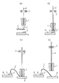
ここで超音波併用熱圧着接合は通常ネールヘッドボンディング方法により行われている。ネールヘッドボンディング方法による接合法を図1を用いて説明する。
図1(a)に示す様にワイヤー2をキャピラリー1に挿通しその先端に電気トーチ3を対向させ、ワイヤー2との間で放電させることにより、ワイヤー2の先端を加熱、溶融してボール4を形成する。
【0004】
次いで図1(b)に示すようにキャピラリー1を下降させて該ボール4をICチップ6上のAl電極5の上に押圧接合する。この時図示しないが超音波振動がキャピラリー1を通して付加されると共に、ICチップ6はヒーターブロックで加熱されるため上記ボール4は熱圧着され圧着ボール4′となる。
次いで図1(c)に示すようにキャピラリー1は所定の軌跡を描いて、外部配線8の上に移動し、下降する。この時図示しないが超音波振動がキャピラリー1を通して付加され、外部配線8はヒーターブロックで加熱されるためワイヤー2側面が熱圧着される。
【0005】
次いで図1(d)に示すようにクランパー7はワイヤー2をクランプしたまま上昇することにより、ワイヤー2が切断され配線が完了する。
一方超音波接合は通常振動を接合部へ伝えるのに最適なウエッジボンディング方法により行われている。これはウエッジ状ツールを用いる方法である。
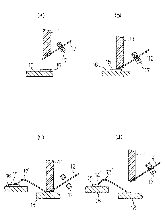
ウエッジボンディング方式による接合法を図2を用いて説明する。
【0006】
図2(a)に示す様にワイヤー12をウエッジ11下端部に挿通し、この下方にICチップ16上のAl電極15を移動する。
次いで図2(b)に示すようにウエッジ11を下降させて常温のまま超音波振動を付加してワイヤー12をAl電極15に接合する。
次いで図2(c)に示すようにクランパー17が開放され、ウエッジ11は所定の軌跡を描いて、外部配線18の上に移動し、下降する。この時図示しないが常温のまま超音波振動がウエッジ11を通して付加され、ワイヤー12を外部配線18に接合する。
【0007】
次いで図2(d)に示すようにクランパー17はワイヤー2をクランプしたままウエッジ11が上昇することにより、ワイヤー12が切断され配線が完了する。
前記ネールヘッドボンディング方法は生産性に優れている為好ましい方法であるが、熱を用いる為ワイヤー材料として金合金線を用いて使用され、酸化し易いアルミ合金線には不適である。
【0008】
また図3(a)に示す様に圧着ボール径L1 がワイヤー外径Dの3〜4倍になることが微細な配線を行う際のネックになるという限界を有している。
次のウエッジボンディング方法は生産性は低下するものの室温で処理出来る為ワイヤー材料としてアルミ合金線を用いて使用されている。また図3(b)に示す様につぶれ幅L2 がワイヤー外径Dの1.5〜2.5倍に抑制出来るという特徴を有している。
【0009】
ここで前述のワイヤー材料として金合金線は他の材料と対比して耐蝕性に優れている為、半導体装置の耐蝕性に対する信頼性を確保する面で配線材料として最も好ましい材料である。
一方最近の半導体装置に対して高密度配線が要求されている。これの対応として金合金線とICチップ電極との接合部の配線方向と直角方向での拡がりを小さくすることが必要である。
【0010】
この為ワイヤー材料として金合金線を用いてネールヘッドボンディングを行うに当たって、圧着ボールの外径を小さくする事が試みられたがその大きさにも限度がある。
【0011】
【発明が解決しようとする課題】
前述の従来事情に鑑み従来からネールヘッドボンディング用として提案されている金合金線を用いてICチップ電極にウエッジボンディングを行ってみたところ、接合部の配線方向と直角方向での拡がりはネールヘッドボンディング方法と対比して小さくすることは出来るものの、ICチップの作動状態を考えて高温状態に晒した後の接合部での接合強度(以下高温接合強度という)が小さく半導体装置の信頼性が低下するという問題が生じてきた。
【0012】
この為本発明に於いては金合金線を用いてICチップ電極にウエッジボンディングを行うことにより、配線方向と直角方向での接合部の拡がりを小さくして高密度配線に対応するとともに高温接合強度を向上させて半導体装置の信頼性を向上させることの出来る金合金線を提供する事を目的とする。
【0013】
【課題を解決するための手段】
本発明者等が鋭意研究を重ねた結果、高純度金に所定量のCa及び所定量のPd,Ag,Ptのうち少なくとも1種を共存し、通常のネールヘッドボンディング用金合金線より伸び率を小さくし且つ引張り強さを大きくした金合金線とすることにより、前記組成と材料特性の相乗効果によって前述の目的を達成し得ることを知見し、本発明を完成するに至った。
【0014】
具体的には、本発明により、下記が提供される。
(1)カルシウム(Ca)を1〜100重量 ppm 、さらに銀(Ag)又は白金(Pt)のうち少なくとも1種を0.2〜5.0重量%含有し、残部が金及び不可避不純物からなる組成を有する金合金線であって該金合金線の引張強さが33.0 kg / mm 2 以上、伸び率が1〜3%であることを特徴とするウエッジボンディング用金合金線。
(2)カルシウム(Ca)を1〜100重量 ppm 、さらに銀(Ag)又は白金(Pt)のうち少なくとも1種及びパラジウム(Pd)を0.2〜5.0重量%含有し、残部が金及び不可避不純物からなる組成を有する金合金線であって該金合金線の引張強さが33.0 kg / mm 2 以上、伸び率が1〜3%であることを特徴とするウエッジボンディング用金合金線。
【0015】
(3)上記(1)(2)において、さらにMg,Y,La,Eu,Ge,Beのうち少なくとも1種を1〜100重量 ppm 添加したウエッジボンディング用金合金線。
(4)カルシウム(Ca)を1〜100重量 ppm 、パラジウム(Pd)を0.2〜5.0重量%、さらにMg又はLaのうち少なくとも1種を1〜100重量 ppm 含有し、残部が金及び不可避不純物からなる組成を有する金合金線であって該金合金線の引張強さが33.0 kg / mm 2 以上、伸び率が1〜3%であることを特徴とするウエッジボンディング用金合金線。
【0016】
【発明の実施の形態】
本発明のウエッジボンディング用金合金線は高純度金に所定量のCaとPd,Ag,Ptのうち少なくとも1種を含有した組成を有し、伸び率を小さくし、引張り強さを大きくすることを特徴とする。
(1)組成
▲1▼ 原料高純度金としては少なくとも99.99重量%以上、好ましくは99.995重量%以上、最も好ましくは99.999重量%以上に精製した高純度金が用いられる。
【0017】
▲2▼ 〔Ca〕
(a)この様な高純度金に上記所定量のCaとPd,Ag,Ptのうち少なくとも1種を共存した組成にするとともに所定の伸び率及び引張り強さとすることにより、その相乗効果によって高温接合強度を向上させる事ができる。
(b)Ca含有量が1重量ppm 未満になると1重量ppm 以上と対比して高温接合強度は小さくなる。Ca含有量が100重量ppm を超えるとICチップに割れが生じる為、これを避けるため不十分な接合しか出来なくなり高温接合強度は小さくなる。
【0018】
この為Ca含有量は伸び率及び引張り強さの条件のもとに1〜100重量ppm と定めた。好ましくは1〜50重量ppm である。
(c)この効果は上記所定量のCaとPd,Ag,Ptのうち少なくとも1種の共存に加えて、Mg,Y,La,Eu,Ge,Beのうち少なくとも1種の成分を1〜100重量ppm の範囲内で添加しても所定の伸び率及び引張り強さを有する金合金線であれば所定量のCa及びPd,Ag,Ptのうち少なくとも1種を共存した効果が維持され高温接合強度を向上させる事ができる。
【0019】
(d)この場合Pd,Ag,Ptのうち少なくとも1種を所定量添加し、所定量のCaを添加しない場合、所定の伸び率及び引張り強さを有しても高温接合強度は小さくなる。
▲3▼ 〔Pd,Ag,Pt〕
(a)前記高純度金に上記所定量のCaとPd,Ag,Ptのうち少なくとも1種を共存して所定量の金純度を有する組成にするとともに所定の伸び率及び引張り強さとすることにより、その相乗効果によって高温接合強度を向上させる事ができる。
【0020】
(b)Pd,Ag,Ptのうち少なくとも1種が0.2重量%未満になると0.2重量%以上と対比して高温接合強度は小さくなる。5.0重量ppm を超えるとICチップに割れが生じる為、これを避けるため不十分な接合しか出来なくなり高温接合強度は小さくなる。
この為Pd,Ag,Ptのうち少なくとも1種の含有量は所定の伸び率及び引張り強さの条件のもとに0.2〜5.0重量%と定めた。
本発明の金合金線は、出発高純度金にやはり高純度の添加元素を添加することにより、得られる金合金線の不純物量を制御することができる。添加元素も99.99重量%以上、さらには99.995重量%以上、99.999重量%以上にすることができるので、得られる金合金線の不純物を100重量ppm 以下、さらには20重量ppm 以下にすることができる。
(2)伸び率
▲1▼ 上記所定量のCaとPd,Ag,Ptのうち少なくとも1種を含有し残部が金及び不可避不純物からなる組成にし、所定の引張り強さにするとともに伸び率を1〜3%とすることにより、その相乗効果によって高温接合強度を向上させる事ができる。
本発明に於いて伸び率は、室温で、金合金線を標点距離を100mmとして引張速度10mm/分で引張試験機で引っ張り、破断した時の伸び量を測定して次式の値を伸び率とする。
【数1】
【0021】
▲2▼ 伸び率が3%を超えると高温接合強度は小さくなる。この為伸び率は1〜3%と定めた。好ましくは2〜3%である。
(3)引張り強さ
▲1▼ 上記所定量のCaとPd,Ag,Ptのうち少なくとも1種を含有し残部が金及び不可避不純物からなる組成にし、所定の伸び率にするとともに引張り強さを33.0kg/mm2 以上とすることにより、その相乗効果によって高温接合強度を向上させる事ができる。
【0022】
▲2▼ 引張り強さが33.0kg/mm2 未満になると33.0kg/mm2 以上と対比して、高温接合強度は小さくなる。
この為引張り強さは33.0kg/mm2 以上と定めた。好ましくは33.0〜70.0kg/mm2 であり、さらに好ましくは33.0〜63.0kg/mm2 である。(4)金合金線の製造方法
本発明になる金合金線の好ましい製造方法を説明する。
【0023】
高純度金に所定量の元素を添加し真空溶解炉で溶解した後インゴットに鋳造する。該当インゴットに溝ロール、伸線機を用いた冷間加工と中間アニールを施し、最終冷間加工により直径10〜100μmの細線とした後最終アニールを施すものである。
ここで本発明になる合金組成の場合、最終アニールの温度が上昇するにつれて伸び率は1〜3%を維持したまま、引張り強さが徐々に低下する温度領域がある。また同一組成であっても最終冷間加工率の大きさによって引張り強さは変わってくる。この為最終冷間加工率と最終アニール温度を制御して伸び率と引張り強さを調整する。このようにして伸び率は1〜3%を維持し、引張り強さが33.0kg/mm2 以上、好ましくは33.0〜70.0kg/mm2 となる温度領域でアニールする事が必要である。更にアニール温度が上昇すると伸び率が4%以上となり引張り強さは更に低下してくる。従来から使用されているネールヘッドボンディング用の金合金線は伸び率が4%以上のものが使用されているが本発明になる金合金線では所定の引張り強さと1〜3%伸び率を与えるために、合金組成に対応した最終冷間加工率を調整し更に低い温度領域でアニールする。
(5)用途
本発明になるウエッジボンディング用金合金線はICチップをリードに接続する方法及びICチップを直接基板に接続するリードレスで接続する方法の何れに用いても好適である。
なお、ここでいうウエッジボンディングとは、ICチップの電極、例えばAl電極と外部リードや他の電極をワイヤーで配線する際、ワイヤーと電極部の接合がファーストボンド、セカンドボンド共にボールを形成することなく、ウエッジ状ツールを用いてワイヤー側面を圧着して接合するボンディングであり、必要に応じてウエッジ状ツールを介して超音波を印加したり電極部を加熱する。
【0024】
【作用】
本発明になる金合金線がウエッジボンディングを行った後高温接合強度に優れている理由は明らかではないが、有効元素としてのCaが添加されていること、有害元素がその含有量を規制されていること、又伸び率が小さく、引張り強さが大きいことがウエッジボンディングによる超音波接合を行う際、材料の不必要な変形を阻止することと相まって生成されるAu−Al金属間化合物が熱的に安定なものが得られているためではないかと考えられる。
【0025】
【実施例】
表1〜3に示す実施例、参考例及び比較例について説明する。
(参考例1)
純度99.999重量%の高純度金に所定量のCa及びPdを添加し真空溶解炉で溶解した後鋳造して表1に示す組成の金合金、即ち1重量ppm Ca、1.0重量%Pd、残部が金及び不可避不純物からなる組成の金インゴットを得、これに溝ロール、伸線機を用いた冷間加工と中間アニールを施し、最終線径25μmとし、最終アニールにより引張り強さが39.8kg/mm2 、伸び率2〜3%になるように仕上げた。
【0026】
この金合金線をウエッジボンディング装置(新川株式会社製 SWB−FA−US30)を用いて前述の図2に示す方法でICチップのAl電極上及び外部配線上に超音波ボンディングを行った。この時ICチップ側のボンディングはボンディング荷重を45g、ボンディング時間を30ms、ボンディングパワーを0.64wの条件で行った。
【0027】
次に試料10個を200℃に設定した高温炉で100時間保持した。次いで試料を炉から取り出し、外部配線側でワイヤーを切断し次の方法でICチップ側の高温接合強度を測定した。即ちICチップ側を治具で固定し、ワイヤーを上方に引っ張り破断荷重を測定した。10個の平均値を測定値とし、測定結果を表1に示す。
(参考例2〜14、実施例1〜37、比較例1〜26)
金及び金合金線の組成、伸び率及び引張り強さを表1に示すようにしたこと以外は参考例1と同様にして細線に仕上げ、超音波ボンディングを行った後高温接合強度を測定した。
【0028】
測定結果を表1〜5に示す。
(試験結果)
(1)高純度金に1〜100重量ppm のCa及び0.2〜5.0重量%のPd,Ag,Ptのうち少なくとも1種を添加した組成であって、伸び率2〜3%、引張強さ39.1〜41.5kg/mm2 である実施例1〜16及び参考例1〜7は高温接合強度が3.5〜5.1gと優れた効果を示した。
【0029】
この中でもCa添加量が1〜50重量ppm のとき高温接合強度が4.1〜5.1gである為好ましく用いられる。
(2)前記組成にMg,Y,La,Eu,Ge,Beのうち少なくとも1種を所定量添加して、伸び率1〜3%(2〜3%)、引張強さ39.2〜41.5kg/mm2 である実施例17〜28及び参考例8〜14は高温接合強度が4.3〜5.1gであり、同様に優れた効果を示していることが判る。
【0030】
(3)参考例3及び実施例3,9,18に示す組成及び伸び率を有し、引張強さが33.0〜60.6kg/mm2 である参考例14,15及び実施例29〜35は高温接合強度が3.8〜4.4gであり優れた効果を示した。
(4)本発明に係わるCa及びPd,Ag,Ptのいずれも含有しない比較例1は高温接合強度が0.6gと悪い事が判る。
【0031】
(5)本発明の必須成分であるCaを含有せず、Pd,Ag,Ptのうち少なくとも1種を含有する比較例2〜5は高温接合強度が2.5〜2.8gと悪い事が判る。
(6)50重量ppm のCaを含有するものの、Pd,Ag,Ptのうち少なくとも1種にかえて2.0重量%のCuを含有し所定の伸び率及び引張強さを有する比較例6は高温接合強度が0.5gと悪い事が判る。
【0032】
(7)所定量のPd,Ag,Ptのうち少なくとも1種を含有するものの、Caの含有量が200重量ppm である比較例7〜10は高温接合強度が1.0〜1.4gと悪い事が判る。
(8)所定量のCaを含有するものの、Pd,Ag,Ptのうち少なくとも1種の含有量が0.11重量%である比較例11〜14は高温接合強度が3.2〜3.3gと悪い事が判る。
【0033】
(9)所定量のCaを含有するものの、Pd,Ag,Ptのうち少なくとも1種の含有量が6.0重量%である比較例15〜18は高温接合強度が1.2〜1.6gと悪い事が判る。
(10)所定量のCa及びPd,Ag,Ptのうち少なくとも1種を含有し、所定の伸び率を有するものの引張り強さが33.0kg/mm2 未満である比較例19〜22は高温接合強度が2.6〜2.9gと悪い事が判る。
【0034】
(11)所定量のCa及びPd,Ag,Ptのうち少なくとも1種を含有し、所定の引張り強さを有するものの伸び率が2〜3%を超える比較例23〜26は高温接合強度が2.0〜2.4gと悪い事が判る。
【0035】
【表1】
【表2】
【表3】
【表4】
【表5】
【発明の効果】
本発明により、請求項に記載の如く、所定量のCa及びPd,Ag,Ptのうち少なくとも1種を含有し残部が金及び不可避不純物からなる組成を有し且つ所定の伸び率と引張り強さを有するウエッジボンディング用金合金線によれば高温接合強度を向上させることが出来半導体装置の信頼性向上に効果的である。前記含有成分に加えて所定量のMg,Y,La,Eu,Ge,Beのうち少なくとも1種を含有した場合においても同様の効果を示すものである。
【図面の簡単な説明】
【図1】ネールボンディング方法による接合法の説明。
【図2】ウエッジボンディング方法による接合法の説明。
【図3】ネールボンディング方法とウエッジボンディング方法による接合部の形状、寸法を示す。
【符号の説明】
11…ウエッジ
12…ワイヤー
12′…ボンディングワイヤー
14′…ワイヤー接合部
15…Al配線
16…ICチップ
17…クランパー
18…外部配線
D…ワイヤ径
L1 …圧着ボール径
L2 …つぶれ幅[0001]
BACKGROUND OF THE INVENTION
The present invention relates to a gold alloy wire for wedge bonding, and is directed to a gold alloy wire excellent in high-temperature bonding strength and suitable for high-density wiring of an IC chip.
[0002]
[Prior art]
When connecting an electrode of an IC chip and external wiring, a wire bonding method of wiring through a wire is known. Among them, the thermocompression bonding with ultrasonic waves and the ultrasonic bonding dominate by the method of bonding the Al electrode of the IC chip and the wire.
[0003]
Here, the ultrasonic thermocompression bonding is usually performed by a nail head bonding method. A bonding method by the nail head bonding method will be described with reference to FIG.
As shown in FIG. 1A, the
[0004]
Next, as shown in FIG. 1B, the capillary 1 is lowered and the ball 4 is pressed and bonded onto the
Next, as shown in FIG. 1C, the capillary 1 moves on the external wiring 8 along a predetermined locus and descends. At this time, although not shown, ultrasonic vibration is applied through the capillary 1 and the external wiring 8 is heated by the heater block, so that the side surface of the
[0005]
Next, as shown in FIG. 1 (d), the
On the other hand, ultrasonic bonding is usually performed by a wedge bonding method that is optimal for transmitting vibration to the bonded portion. This is a method using a wedge-shaped tool.
A bonding method using the wedge bonding method will be described with reference to FIG.
[0006]
As shown in FIG. 2A, the
Next, as shown in FIG. 2B, the
Next, as shown in FIG. 2C, the
[0007]
Next, as shown in FIG. 2 (d), the
The nail head bonding method is preferable because it is excellent in productivity. However, since it uses heat, it is used as a wire material using a gold alloy wire and is not suitable for an aluminum alloy wire that is easily oxidized.
[0008]
Further, as shown in FIG. 3A, there is a limit that the pressure ball diameter L 1 being 3 to 4 times the wire outer diameter D becomes a bottleneck when fine wiring is performed.
The following wedge bonding method is used by using an aluminum alloy wire as a wire material because it can be processed at room temperature although the productivity is lowered. The width L 2 crushed as shown in FIG. 3 (b) has a feature that can be reduced to 1.5 to 2.5 times the wire outer diameter D.
[0009]
Here, since the gold alloy wire is superior in corrosion resistance as compared with other materials as the above-mentioned wire material, it is the most preferable material as the wiring material in terms of ensuring the reliability with respect to the corrosion resistance of the semiconductor device.
On the other hand, high-density wiring is required for recent semiconductor devices. To cope with this, it is necessary to reduce the spread in the direction perpendicular to the wiring direction of the joint portion between the gold alloy wire and the IC chip electrode.
[0010]
For this reason, when performing nail head bonding using a gold alloy wire as a wire material, attempts have been made to reduce the outer diameter of the press-bonded ball, but the size is also limited.
[0011]
[Problems to be solved by the invention]
In view of the above-mentioned conventional circumstances, when performing wedge bonding on the IC chip electrode using a gold alloy wire that has been proposed for nail head bonding, the spread in the direction perpendicular to the wiring direction of the joint is nail head bonding. Although it can be reduced compared to the method, the bonding strength (hereinafter referred to as high temperature bonding strength) at the bonded portion after exposure to a high temperature state in consideration of the operating state of the IC chip is small and the reliability of the semiconductor device is lowered. The problem has arisen.
[0012]
For this reason, in the present invention, wedge bonding is performed on the IC chip electrode by using a gold alloy wire, thereby reducing the spread of the joint in the direction perpendicular to the wiring direction and supporting high-density wiring and high-temperature bonding strength. An object of the present invention is to provide a gold alloy wire that can improve the reliability of a semiconductor device.
[0013]
[Means for Solving the Problems]
As a result of intensive studies by the present inventors, high purity gold coexists with a predetermined amount of Ca and a predetermined amount of Pd, Ag, and Pt, and the elongation rate is higher than that of a normal gold alloy wire for nail head bonding. It has been found that the above-mentioned object can be achieved by a synergistic effect of the composition and material characteristics by making the gold alloy wire having a small tensile strength and a high tensile strength, and the present invention has been completed.
[0014]
Specifically, the present invention provides the following.
(1) 1-100 ppm by weight of calcium (Ca) , further containing 0.2-5.0% by weight of at least one of silver (Ag) or platinum (Pt), with the balance being gold and inevitable impurities A gold alloy wire having a composition, wherein the tensile strength of the gold alloy wire is 33.0 kg / mm 2 As described above, a gold alloy wire for wedge bonding characterized by an elongation of 1 to 3%.
(2) 1-100 ppm by weight of calcium (Ca) , further containing at least one of silver (Ag) or platinum (Pt) and 0.2-5.0% by weight of palladium (Pd), with the balance being gold And a gold alloy wire having a composition comprising inevitable impurities, the tensile strength of the gold alloy wire being 33.0 kg / mm 2 As described above, a gold alloy wire for wedge bonding characterized by an elongation of 1 to 3%.
[0015]
( 3) A gold alloy wire for wedge bonding in which at least one of Mg, Y, La, Eu, Ge, and Be is added in an amount of 1 to 100 ppm by weight in the above (1) and (2) .
(4) 1-100 ppm by weight of calcium (Ca), 0.2-5.0% by weight of palladium (Pd), 1-100 ppm by weight of at least one of Mg or La , the balance being gold And a gold alloy wire having a composition comprising inevitable impurities, the tensile strength of the gold alloy wire being 33.0 kg / mm 2 As described above, a gold alloy wire for wedge bonding characterized by an elongation of 1 to 3%.
[0016]
DETAILED DESCRIPTION OF THE INVENTION
The gold alloy wire for wedge bonding of the present invention has a composition containing a predetermined amount of Ca and at least one of Ca, Pd, Ag, and Pt in high-purity gold, and reduces the elongation and increases the tensile strength. It is characterized by.
(1) Composition {circle around (1)} High purity gold purified to at least 99.99% by weight or more, preferably 99.995% by weight or more, and most preferably 99.999% by weight or more is used.
[0017]
▲ 2 ▼ [Ca]
(A) In such high-purity gold, a composition in which at least one of the predetermined amount of Ca and Pd, Ag, and Pt coexists and a predetermined elongation and tensile strength are used, and the synergistic effect increases the temperature. Bonding strength can be improved.
(B) When the Ca content is less than 1 ppm by weight, the high-temperature bonding strength becomes small as compared with 1 ppm by weight or more. When the Ca content exceeds 100 ppm by weight, the IC chip is cracked, and in order to avoid this, only insufficient bonding can be performed and the high-temperature bonding strength is reduced.
[0018]
For this reason, the Ca content is determined to be 1 to 100 ppm by weight under the conditions of elongation and tensile strength. Preferably, it is 1 to 50 ppm by weight.
(C) In addition to the coexistence of at least one of the predetermined amount of Ca and Pd, Ag, and Pt, this effect is achieved by adding at least one component of Mg, Y, La, Eu, Ge, and Be to 1 to 100. Even if it is added within the range of ppm by weight, the effect of coexisting at least one of Ca and Pd, Ag and Pt in a predetermined amount is maintained as long as it is a gold alloy wire having a predetermined elongation and tensile strength. Strength can be improved.
[0019]
(D) In this case, when a predetermined amount of at least one of Pd, Ag, and Pt is added and a predetermined amount of Ca is not added, the high-temperature bonding strength is reduced even if the predetermined elongation and tensile strength are obtained.
(3) [Pd, Ag, Pt]
(A) By making the composition having a predetermined amount of gold purity by coexisting at least one of the predetermined amount of Ca and Pd, Ag, Pt with the high-purity gold, and having a predetermined elongation and tensile strength. The high temperature bonding strength can be improved by the synergistic effect.
[0020]
(B) When at least one of Pd, Ag, and Pt is less than 0.2% by weight, the high-temperature bonding strength becomes small as compared with 0.2% by weight or more. If it exceeds 5.0 ppm by weight, cracks occur in the IC chip, and in order to avoid this, only insufficient bonding is possible and the high-temperature bonding strength is reduced.
For this reason, the content of at least one of Pd, Ag, and Pt is determined to be 0.2 to 5.0% by weight under the conditions of a predetermined elongation and tensile strength.
In the gold alloy wire of the present invention, the amount of impurities in the resulting gold alloy wire can be controlled by adding a high purity additive element to the starting high purity gold. Since the additive element can be 99.99% by weight or more, further 99.995% by weight or more, 99.999% by weight or more, the impurities of the obtained gold alloy wire are 100 ppm by weight or less, and further 20 ppm by weight. It can be:
(2) Elongation rate (1) The composition contains at least one of the predetermined amount of Ca and Pd, Ag, and Pt, and the balance is made of gold and inevitable impurities, and has a predetermined tensile strength and an elongation rate of 1 By setting the content to ˜3%, the high-temperature bonding strength can be improved by the synergistic effect.
In the present invention, the elongation is measured by measuring the elongation when a gold alloy wire is pulled with a tensile tester at a tensile speed of 10 mm / min at a room temperature and the gauge distance is 100 mm, and the value of the following formula is extended. Rate.
[Expression 1]
[0021]
(2) When the elongation exceeds 3%, the high-temperature bonding strength decreases. For this reason, the elongation was determined to be 1 to 3%. Preferably it is 2-3%.
(3) Tensile strength {circle around (1)} A composition containing at least one of the predetermined amount of Ca and Pd, Ag, and Pt, with the balance being made of gold and inevitable impurities, with a predetermined elongation, and a tensile strength. By setting it to 33.0 kg / mm 2 or more, the high-temperature bonding strength can be improved by the synergistic effect.
[0022]
▲ 2 ▼ tensile strength in contrast to the less than 33.0kg / mm 2 33.0kg / mm 2 or more, the high temperature bond strength is reduced.
For this reason, the tensile strength was set to 33.0 kg / mm 2 or more. Preferably it is 33.0-70.0 kg / mm < 2 >, More preferably, it is 33.0-63.0 kg / mm < 2 >. (4) Method for Producing Gold Alloy Wire A preferred method for producing the gold alloy wire according to the present invention will be described.
[0023]
A predetermined amount of element is added to high-purity gold, melted in a vacuum melting furnace, and cast into an ingot. The ingot is subjected to cold processing and intermediate annealing using a groove roll and a wire drawing machine, and is subjected to final annealing after the final cold processing is performed to form a thin wire having a diameter of 10 to 100 μm.
Here, in the case of the alloy composition according to the present invention, there is a temperature range in which the tensile strength gradually decreases while the elongation rate is maintained at 1 to 3% as the final annealing temperature increases. Even with the same composition, the tensile strength varies depending on the final cold work rate. Therefore, the elongation rate and the tensile strength are adjusted by controlling the final cold working rate and the final annealing temperature. Thus, it is necessary to anneal in a temperature range in which the elongation is maintained at 1 to 3% and the tensile strength is 33.0 kg / mm 2 or more, preferably 33.0 to 70.0 kg / mm 2. is there. Further, when the annealing temperature rises, the elongation becomes 4% or more, and the tensile strength further decreases. Conventionally used gold alloy wires for nail head bonding have an elongation of 4% or more, but the gold alloy wire according to the present invention gives a predetermined tensile strength and 1-3% elongation. Therefore, the final cold working rate corresponding to the alloy composition is adjusted and annealing is performed in a lower temperature region.
(5) Application The gold alloy wire for wedge bonding according to the present invention is suitable for any of a method of connecting an IC chip to a lead and a method of connecting an IC chip directly to a substrate by a leadless connection.
Wedge bonding here refers to IC ball electrodes such as Al electrodes and external leads or other electrodes wired with wires, and the bonding between the wire and the electrode part forms a ball for both the first bond and the second bond. Rather, the bonding is performed by crimping and bonding the side surfaces of the wire using a wedge-shaped tool, and applying an ultrasonic wave or heating the electrode part via the wedge-shaped tool as necessary.
[0024]
[Action]
The reason why the gold alloy wire according to the present invention is excellent in high-temperature bonding strength after performing wedge bonding is not clear, but Ca is added as an effective element, and the content of harmful elements is regulated. In addition, the fact that the elongation rate is small and the tensile strength is large is that the Au-Al intermetallic compound formed in combination with preventing unnecessary deformation of the material is thermally coupled with ultrasonic bonding by wedge bonding. This is probably because a stable product is obtained.
[0025]
【Example】
Examples , reference examples and comparative examples shown in Tables 1 to 3 will be described.
( Reference Example 1 )
A predetermined amount of Ca and Pd is added to high-purity gold having a purity of 99.999% by weight, melted in a vacuum melting furnace, and then cast to be a gold alloy having the composition shown in Table 1, that is, 1 wt ppm Ca, 1.0 wt% A gold ingot having a composition composed of Pd, the balance being gold and inevitable impurities is obtained, and this is subjected to cold working and intermediate annealing using a groove roll and a wire drawing machine to obtain a final wire diameter of 25 μm. It finished so that it might become 39.8 kg / mm < 2 > and elongation rate 2-3%.
[0026]
This gold alloy wire was subjected to ultrasonic bonding on the Al electrode of the IC chip and on the external wiring by the method shown in FIG. 2 using a wedge bonding apparatus (SWB-FA-US30 manufactured by Shinkawa Co., Ltd.). At this time, bonding on the IC chip side was performed under the conditions of a bonding load of 45 g, a bonding time of 30 ms, and a bonding power of 0.64 w.
[0027]
Next, 10 samples were held in a high temperature furnace set at 200 ° C. for 100 hours. Next, the sample was taken out of the furnace, the wire was cut on the external wiring side, and the high-temperature bonding strength on the IC chip side was measured by the following method. That is, the IC chip side was fixed with a jig, the wire was pulled upward, and the breaking load was measured. The average value of 10 pieces is taken as a measurement value, and the measurement results are shown in Table 1.
( Reference Examples 2-14, Examples 1-37 , Comparative Examples 1-26)
Except that the composition, elongation rate and tensile strength of the gold and gold alloy wires were as shown in Table 1, the wires were finished in the same manner as in Reference Example 1 and subjected to ultrasonic bonding, and then the high temperature bonding strength was measured.
[0028]
The measurement results are shown in Tables 1-5.
(Test results)
(1) A composition obtained by adding at least one of high purity gold of 1 to 100 ppm by weight of Ca and 0.2 to 5.0% by weight of Pd, Ag, and Pt, with an elongation of 2 to 3%, Examples 1 to 16 and Reference Examples 1 to 7 having a tensile strength of 39.1 to 41.5 kg / mm 2 exhibited an excellent effect of high temperature bonding strength of 3.5 to 5.1 g.
[0029]
Among these, when the Ca addition amount is 1 to 50 ppm by weight, the high-temperature bonding strength is 4.1 to 5.1 g, so that it is preferably used.
(2) A predetermined amount of at least one of Mg, Y, La, Eu, Ge, and Be is added to the composition to obtain an elongation of 1 to 3% (2 to 3%) and a tensile strength of 39.2 to 41. It can be seen that Examples 17 to 28 and Reference Examples 8 to 14 which are .5 kg / mm 2 have a high-temperature bonding strength of 4.3 to 5.1 g, and similarly show excellent effects.
[0030]
(3) Reference Examples 14 and 15 and Examples 29 to 29 having the composition and elongation shown in Reference Example 3 and Examples 3, 9, and 18 and having a tensile strength of 33.0 to 60.6 kg / mm 2. No. 35 had a high-temperature bonding strength of 3.8 to 4.4 g, showing an excellent effect.
(4) It can be seen that Comparative Example 1 which does not contain any of Ca and Pd, Ag, and Pt according to the present invention has a high-temperature bonding strength of 0.6 g.
[0031]
(5) Comparative Examples 2 to 5 that do not contain Ca, which is an essential component of the present invention, and contain at least one of Pd, Ag, and Pt have a high temperature bonding strength of 2.5 to 2.8 g. I understand.
(6) Although it contains 50 ppm by weight of Ca, Comparative Example 6 containing 2.0% by weight of Cu instead of at least one of Pd, Ag, and Pt and having a predetermined elongation and tensile strength is It can be seen that the high-temperature bonding strength is poor at 0.5 g.
[0032]
(7) Although containing at least one of a predetermined amount of Pd, Ag, and Pt, Comparative Examples 7 to 10 having a Ca content of 200 ppm by weight have poor high-temperature bonding strength of 1.0 to 1.4 g. I understand that.
(8) Although containing a predetermined amount of Ca, Comparative Examples 11 to 14 in which the content of at least one of Pd, Ag, and Pt is 0.11% by weight has a high-temperature bonding strength of 3.2 to 3.3 g. I understand that it is bad.
[0033]
(9) Although containing a predetermined amount of Ca, Comparative Examples 15 to 18 in which the content of at least one of Pd, Ag, and Pt is 6.0% by weight has a high-temperature bonding strength of 1.2 to 1.6 g. I understand that it is bad.
(10) Comparative Examples 19-22, which contain a predetermined amount of Ca and at least one of Pd, Ag, Pt, have a predetermined elongation, but have a tensile strength of less than 33.0 kg / mm 2 are high temperature bonding It can be seen that the strength is as bad as 2.6 to 2.9 g.
[0034]
(11) Comparative Examples 23 to 26, which contain a predetermined amount of Ca and at least one of Pd, Ag, and Pt and have a predetermined tensile strength and have an elongation of more than 2 to 3%, have a high-temperature bonding strength of 2 It turns out that it is bad with 0.0-2.4g.
[0035]
[Table 1]
[Table 2]
[Table 3]
[Table 4]
[Table 5]
【The invention's effect】
According to the present invention , as set forth in the claims, it has a composition containing at least one of a predetermined amount of Ca and Pd, Ag, Pt, the balance being gold and inevitable impurities, and a predetermined elongation and tensile strength. According to the gold alloy wire for wedge bonding having high temperature, the high-temperature bonding strength can be improved, which is effective for improving the reliability of the semiconductor device. In the case where at least one of Mg, Y, La, Eu, Ge, and Be in a predetermined amount is contained in addition to the above-described components, the same effect is exhibited.
[Brief description of the drawings]
FIG. 1 is a diagram illustrating a bonding method using a nail bonding method.
FIG. 2 is a diagram illustrating a bonding method using a wedge bonding method.
FIG. 3 shows the shape and dimensions of a joint by a nail bonding method and a wedge bonding method.
[Explanation of symbols]
11 ... wedge 12 ... Wire 12 '... bonding wire 14' ...
Claims (4)
Priority Applications (1)
| Application Number | Priority Date | Filing Date | Title |
|---|---|---|---|
| JP20616197A JP3690902B2 (en) | 1996-07-31 | 1997-07-31 | Gold alloy wire for wedge bonding |
Applications Claiming Priority (3)
| Application Number | Priority Date | Filing Date | Title |
|---|---|---|---|
| JP20241396 | 1996-07-31 | ||
| JP8-202413 | 1996-07-31 | ||
| JP20616197A JP3690902B2 (en) | 1996-07-31 | 1997-07-31 | Gold alloy wire for wedge bonding |
Publications (2)
| Publication Number | Publication Date |
|---|---|
| JPH1098062A JPH1098062A (en) | 1998-04-14 |
| JP3690902B2 true JP3690902B2 (en) | 2005-08-31 |
Family
ID=26513361
Family Applications (1)
| Application Number | Title | Priority Date | Filing Date |
|---|---|---|---|
| JP20616197A Expired - Fee Related JP3690902B2 (en) | 1996-07-31 | 1997-07-31 | Gold alloy wire for wedge bonding |
Country Status (1)
| Country | Link |
|---|---|
| JP (1) | JP3690902B2 (en) |
Families Citing this family (6)
| Publication number | Priority date | Publication date | Assignee | Title |
|---|---|---|---|---|
| KR100899322B1 (en) * | 2004-09-30 | 2009-05-27 | 타나카 덴시 코오교오 카부시키가이샤 | Au ALLOY BONDING WIRE |
| JP4641248B2 (en) * | 2004-12-21 | 2011-03-02 | 田中電子工業株式会社 | Gold alloy wire for bonding wires with excellent bondability, straightness and resin flow resistance |
| JP4195495B1 (en) * | 2007-11-06 | 2008-12-10 | 田中電子工業株式会社 | Gold alloy wire for ball bonding |
| JP5024907B2 (en) * | 2010-01-06 | 2012-09-12 | 田中電子工業株式会社 | Gold (Au) alloy bonding wire |
| JP5403436B2 (en) * | 2010-10-08 | 2014-01-29 | タツタ電線株式会社 | Ball bonding wire |
| WO2012117512A1 (en) * | 2011-03-01 | 2012-09-07 | 田中電子工業株式会社 | BONDING WIRE OF GOLD (Au) ALLOY |
-
1997
- 1997-07-31 JP JP20616197A patent/JP3690902B2/en not_active Expired - Fee Related
Also Published As
| Publication number | Publication date |
|---|---|
| JPH1098062A (en) | 1998-04-14 |
Similar Documents
| Publication | Publication Date | Title |
|---|---|---|
| EP0822264B1 (en) | Use of a gold alloy wire for wedge bonding | |
| JP3328135B2 (en) | Gold alloy wire for bump formation and bump formation method | |
| JP3382918B2 (en) | Gold wire for connecting semiconductor elements | |
| JP3690902B2 (en) | Gold alloy wire for wedge bonding | |
| JP3657087B2 (en) | Gold alloy wire for wedge bonding | |
| JPH0291944A (en) | Gold alloy fine wire for gold bump | |
| JP3628139B2 (en) | Gold alloy wire for semiconductor element bonding | |
| JP3323185B2 (en) | Gold wire for connecting semiconductor elements | |
| JPH02215140A (en) | Fine gold alloy wire for semiconductor element and its bonding method | |
| KR930001265B1 (en) | Bonding wir for semiconductor elements | |
| JP2000150562A (en) | Bonding gold alloy fine wire for semiconductor device | |
| JP3445616B2 (en) | Gold alloy wires for semiconductor devices | |
| JP4134261B1 (en) | Gold alloy wire for ball bonding | |
| JP3586909B2 (en) | Bonding wire | |
| JP3615901B2 (en) | Gold alloy wire for semiconductor element bonding | |
| JP3669810B2 (en) | Gold alloy wire for semiconductor element bonding | |
| JP3764629B2 (en) | Semiconductor device with wire wedge-bonded | |
| JP3085090B2 (en) | Bonding wire | |
| JPS5826662B2 (en) | Gold wire for bonding semiconductor devices | |
| JPH104114A (en) | Bonding wire | |
| JP3358295B2 (en) | Bonding wire | |
| JP3907534B2 (en) | Gold alloy wire for bonding | |
| JP3744131B2 (en) | Bonding wire | |
| JPH0131691B2 (en) | ||
| JPH11340264A (en) | Method for forming wire bump and gold alloy wire there for |
Legal Events
| Date | Code | Title | Description |
|---|---|---|---|
| A621 | Written request for application examination |
Free format text: JAPANESE INTERMEDIATE CODE: A621 Effective date: 20040527 |
|
| A977 | Report on retrieval |
Free format text: JAPANESE INTERMEDIATE CODE: A971007 Effective date: 20050128 |
|
| A131 | Notification of reasons for refusal |
Free format text: JAPANESE INTERMEDIATE CODE: A131 Effective date: 20050208 |
|
| A521 | Request for written amendment filed |
Free format text: JAPANESE INTERMEDIATE CODE: A523 Effective date: 20050404 |
|
| TRDD | Decision of grant or rejection written | ||
| A01 | Written decision to grant a patent or to grant a registration (utility model) |
Free format text: JAPANESE INTERMEDIATE CODE: A01 Effective date: 20050517 |
|
| A61 | First payment of annual fees (during grant procedure) |
Free format text: JAPANESE INTERMEDIATE CODE: A61 Effective date: 20050614 |
|
| R150 | Certificate of patent or registration of utility model |
Free format text: JAPANESE INTERMEDIATE CODE: R150 |
|
| S531 | Written request for registration of change of domicile |
Free format text: JAPANESE INTERMEDIATE CODE: R313531 |
|
| R350 | Written notification of registration of transfer |
Free format text: JAPANESE INTERMEDIATE CODE: R350 |
|
| FPAY | Renewal fee payment (event date is renewal date of database) |
Free format text: PAYMENT UNTIL: 20090624 Year of fee payment: 4 |
|
| FPAY | Renewal fee payment (event date is renewal date of database) |
Free format text: PAYMENT UNTIL: 20090624 Year of fee payment: 4 |
|
| FPAY | Renewal fee payment (event date is renewal date of database) |
Free format text: PAYMENT UNTIL: 20100624 Year of fee payment: 5 |
|
| FPAY | Renewal fee payment (event date is renewal date of database) |
Free format text: PAYMENT UNTIL: 20110624 Year of fee payment: 6 |
|
| FPAY | Renewal fee payment (event date is renewal date of database) |
Free format text: PAYMENT UNTIL: 20110624 Year of fee payment: 6 |
|
| FPAY | Renewal fee payment (event date is renewal date of database) |
Free format text: PAYMENT UNTIL: 20120624 Year of fee payment: 7 |
|
| FPAY | Renewal fee payment (event date is renewal date of database) |
Free format text: PAYMENT UNTIL: 20120624 Year of fee payment: 7 |
|
| FPAY | Renewal fee payment (event date is renewal date of database) |
Free format text: PAYMENT UNTIL: 20130624 Year of fee payment: 8 |
|
| LAPS | Cancellation because of no payment of annual fees |