JP3674618B2 - Liquid crystal device and electronic device, TFT array substrate for liquid crystal device - Google Patents
Liquid crystal device and electronic device, TFT array substrate for liquid crystal device Download PDFInfo
- Publication number
- JP3674618B2 JP3674618B2 JP2003193077A JP2003193077A JP3674618B2 JP 3674618 B2 JP3674618 B2 JP 3674618B2 JP 2003193077 A JP2003193077 A JP 2003193077A JP 2003193077 A JP2003193077 A JP 2003193077A JP 3674618 B2 JP3674618 B2 JP 3674618B2
- Authority
- JP
- Japan
- Prior art keywords
- thin film
- data lines
- signal
- liquid crystal
- precharge
- Prior art date
- Legal status (The legal status is an assumption and is not a legal conclusion. Google has not performed a legal analysis and makes no representation as to the accuracy of the status listed.)
- Expired - Lifetime
Links
Images


Description
【0001】
【発明の属する技術分野】
本発明は、薄膜トランジスタ(以下、TFTと称す)駆動によるマトリクス駆動方式の液晶装置及びこれを用いた電子機器の技術分野に属し、特に、サンプリング回路及びプリチャージ回路がTFTアレイ基板上に形成される形式の液晶装置及びこれを用いた電子機器の技術分野に属する。
【0002】
【従来の技術】
従来、TFT駆動によるアクティブマトリクス駆動方式の液晶装置においては、縦横に夫々配列された多数の走査線及びデータ線並びにこれらの各交点に対応して多数の画素電極がTFTアレイ基板上に設けられている。そして、これらに加えて、サンプリング回路、プリチャージ回路、走査線駆動回路、データ線駆動回路、検査回路などのTFTを構成要素とする各種の周辺回路が、このようなTFTアレイ基板上に設けられる場合がある。
【0003】
これらの周辺回路のうち、サンプリング回路は、高周波数の画像信号を各データ線に所定のタイミングで安定的に走査信号と同期して供給するために、画像信号をサンプリングする回路である。サンプリング回路のサンプリング能力に応じて、当該サンプリング回路に入力する画像信号の相展開の数が定まる。即ち、水平方向の画素数を固定して考えた場合には、このサンプリング能力が高い程、画像信号の相展開の数を減らすことが出来る。この結果、高解像度の表示を行うために画像信号処理回路等の画像信号の信号源にかかる負担が、サンプリング回路により軽減される。
【0004】
プリチャージ回路は、コントラスト比の向上、データ線の電位レベルの安定、表示画面上のラインむらの低減等を目的として、データ線に対し、データ線駆動回路から上述のサンプリング回路を介して又は直接に供給される画像信号に先行するタイミングで、プリチャージ信号(画像補助信号)を供給することにより、画像信号をデータ線に書込む際の負荷を軽減する回路である。特に液晶を交流駆動するために通常行われるデータ線の電圧極性を所定周期で反転して駆動する所謂1H反転駆動方式(走査線単位で反転する駆動方式)等においては、プリチャージ信号をデータ線に予め書き込んでおけば、画像信号をデータ線に書込む際に必要な電荷量を顕著に少なくできる。例えば、特開平7−295520号公報に、このようなプリチャージ回路の一例が開示されている。
【0005】
以上のように、サンプリング回路やプリチャージ回路などの周辺回路をTFTアレイ基板上に設けることにより、駆動装置等のハードウエア資源にかかる負担を軽減しながら、高品位画像の表示が可能となる。
【0006】
【発明が解決しようとする課題】
液晶パネルやこれに周辺回路を加えた液晶表示モジュールのサイズが同じであれば、マトリクス状に配置された複数の画素電極により規定される画面表示領域、即ち液晶パネル上で実際に液晶の配向状態の変化により画像が表示される領域は、表示装置の基本的要請として大きい程よいとされている。従って、周辺回路は、画面表示領域の周囲に位置するTFTアレイ基板の狭く細長い周辺部分に設けられるのが一般的である。
【0007】
しかしながら、上述したサンプリング回路及びプリチャージ回路を、何等の工夫もなく単にこのようなTFTアレイ基板の狭く細長い周辺部分に設けたのでは、肝心の走査線駆動回路やデータ線駆動回路等を設けるスペースが小さくなってしまい、特定の仕様に沿うようにこれらの周辺回路を設計することが困難になるという問題点がある。
【0008】
また特に、サンプリング回路及びプリチャージ回路は、上述の如きサンプリング機能及びプリチャージ機能を夫々発揮するためには、それらの主たる構成要素である各TFTにおいて、かなり高い電流供給能力が必要となる。更に、これらの回路を構成するTFTは、電圧保持時にオフ状態でも電流が若干リークするため、そのチャネル長は、リーク電流を抑えるためにある程度長くなければならない。従って、TFTサイズを安易に小さくすることは出来ない。そして、このようにチャネル長を短くすることに制限があると、高い電流供給能力を実現するためには、実践上はTFTのサイズを大きくするしかない。このように、サンプリング回路及びプリチャージ回路を設けるスペースを、それらの機能を維持しつつ、小さくすることは困難であるという問題点がある。
【0009】
更に、このようなスペースの問題を抜きにしても、十分なプリチャージを行うためにプリチャージ回路のTFTサイズを余りに大きくしてしまうと、確かに電荷供給は十分に行えるものの、ゲート容量が大きくなってしまい、プリチャージの遅延の問題が生じてしまう。
【0010】
本発明は上述した問題点に鑑みなされたものであり、必要とされるサンプリング機能及びプリチャージ機能を夫々持つと共に基板上に占めるスペースが極力小さいサンプリング回路及びプリチャージ回路を備えており、液晶パネルや液晶表示モジュールのサイズと比較して相対的に有効表示面積が大きく且つ高品位の画像表示が可能な液晶装置及び当該液晶装置を備えた電子機器を提供することを課題とする。
【0011】
【課題を解決するための手段】
本発明の液晶装置は上記課題を解決するために、一対の基板間に液晶が挟持されてなり、前記一対の基板の一方の基板上には、画像信号が供給される複数のデータ線と、前記複数のデータ線に交差する複数の走査線と、前記複数のデータ線と走査線に対応して設けられた複数のスイッチング素子と、前記複数のスイッチング素子に対応して設けられた複数の画素電極と、前記複数のデータ線と前記画像信号の信号源との間に夫々介在する複数の第1薄膜トランジスタを有し、該複数の第1薄膜トランジスタが夫々オンされることで、前記画像信号をサンプリングし前記複数のデータ線に夫々供給するサンプリング回路と、前記複数のデータ線と所定電圧値のプリチャージ信号が供給されるプリチャージ信号線との間に夫々介在する複数の第2薄膜トランジスタを有し、該複数の第2薄膜トランジスタが夫々オンされることで、前記複数のデータ線に前記プリチャージ信号を前記画像信号に先行して夫々供給するプリチャージ回路とを備えており、
薄膜トランジスタがオンされた状態でソース、ドレイン間にかかる所定電圧に応じてチャネルを介して供給できる電流量を薄膜トランジスタの電流供給能力とした時、前記データ線一本に対する前記第1薄膜トランジスタの電流供給能力A1及び前記第2薄膜トランジスタの電流供給能力A2並びに前記データ線一本に対して前記第1薄膜トランジスタの前記画像信号を書込む時間△T1及び前記第2薄膜トランジスタの前記プリチャージ信号を書込む時間△T2との間に、(△T1/△T2)×A1≒A2なる関係が成立するように前記第1及び第2薄膜トランジスタが夫々構成されていることを特徴とする。
【0012】
この液晶装置によれば、先ず複数の第2TFTが夫々オンされると、プリチャージ回路により、プリチャージ信号は、画像信号に先行して複数のデータ線に夫々供給される。そして、各データ線にプリチャージ信号としての電荷が供給されると、その電荷量に応じた分だけ、その後当該データ線を介して画素電極に供給される画像信号の電荷量は少なくて済む。特に前述した1H反転駆動方式のように各画素に対して電圧極性を反転させて画像信号を供給する場合には、このようなプリチャージ信号の供給による画像信号に必要な電荷量の減少は顕著となる。次に、TFT等の複数のスイッチング素子は、例えばそのゲート電極に入力される走査信号に応じて、データ線と画素電極との間(例えば、ソース−ドレイン間)における導通状態及び非導通状態を夫々制御する。そして、このスイッチング素子が、例えば走査信号が供給された際にこの間を導通状態とすると、サンプリング回路からの画像信号がデータ線を介して当該画素電極に供給される。すると、画素電極に印加された液晶印加電圧(例えば、他方の基板に設けられた共通電極の電位と当該画素電極の電位との差)に応じて、対応する液晶部分の配向状態が変化する。このようなプリチャージ信号、画像信号及び走査信号の供給が複数の走査線及びデータ線を介して各画素電極に対して線順次、点順次等の所定の順序で行わる。この結果、当該液晶装置において複数の画素電極により規定される画面表示領域には、液晶の配向状態の変化の分布により画像信号に対応する画像が表示される。
【0013】
ここで特に、サンプリング回路により画素電極に画像信号を書込むのに必要な時間は、各画素電極における液晶部分に液晶印加電圧が印加される周波数であるドット周波数と、画像信号をサンプリング回路に供給するデータ線駆動回路(シフトレジスタ等)の系列数及び方式とに依存する。例えば、XGA方式の液晶パネルで、データ線を12本同時に駆動する場合であって、画像信号のドット周波数が65MHzで垂直周波数が約60Hzの時には、サンプリング回路により一つの画素電極に画像信号としての電荷を書込むのに必要な時間は、約150nsec(ナノ秒)となる。これに対して、例えば水平帰線期間に全てのデータ線を同時にプリチャージする場合に、プリチャージ信号としての電荷を書込むのに必要な時間は、前段の走査線に印加される走査信号がオフして画像信号の極性が反転してから、データ線駆動回路に、そのシフトレジスタの転送動作を開始させるスタート信号が供給されるまでの間における、信号の遅延等を考慮すると、を約2μsecとなる。従って、この場合には、プリチャージ回路の第2TFTの電流供給能力A2は、サンプリング回路の電流供給能力A1の1/10程度で十分であることになる。
【0014】
そこで本発明では、より一般的に、データ線一本に対する第1TFTの電流供給能力A1及び第2TFTの電流供給能力A2並びにデータ線一本に対して第1TFTの画像信号を書込む時間△T1及び第2TFTのプリチャージ信号を書込む時間△T2との間に、(△T1/△T2)×A1≒A2なる関係が成立するように第1及び第2TFTを夫々構成する。ここに、TFTの電流供給能力とは、オンされた状態のTFTが、ソース及びドレイン間にかかる所定電圧に応じてそれらの間にあるチャネルを介して供給できる電流量であり、単位時間当りに供給可能な電荷量に等しい。従って、このような関係が成立すれば、プリチャージ回路が有する第2TFTの電流供給能力A2は、サンプリング回路から供給される画像信号に対してプリチャージの効果を発揮するために必要なレベル以上となる。そして、第2TFTは、必要最低限の電流供給能力A2に対応した必用最低限のサイズを持ち、第2TFTひいてはプリチャージ回路の占有面積をほぼ限界まで小さくできることになる。
【0015】
また本発明の液晶装置は、前記第1薄膜トランジスタのチャネル長と前記第2薄膜トランジスタのチャネル長とは相等しく、前記データ線一本に対して前記第1薄膜トランジスタの前記画像信号を書込む時間△T1、前記第2薄膜トランジスタの前記プリチャージ信号を書込む時間△T2、前記第1薄膜トランジスタのチャネル幅W1、前記第2薄膜トランジスタのチャネル幅W2との間に、(△T1/△T2)×W1≒W2なる関係が成立するように前記第1及び第2薄膜トランジスタが夫々構成されていることを特徴とする。
【0016】
この液晶装置によれば、第2TFTを、必要最低限のチャネル幅W2を持ち、第2TFTひいてはプリチャージ回路の占有面積をほぼ限界まで小さくできることになる。
【0019】
また、本発明の液晶装置は、前記プリチャージ回路は、前記画像信号の水平帰線期間に前記プリチャージ信号を前記複数のデータ線に同時に供給すると良い。
【0020】
この液晶装置によれば、プリチャージ信号は、プリチャージ回路により、画像信号の水平帰線期間に複数のデータ線に同時に供給される。従って、プリチャージ回路には、複数のデータ線に対応する比較的高い電流供給能力A2が必要となるが、(ΔT1/ΔT2)×A1≦A2なる関係が成立するように第1及び第2TFTが夫々構成されているので、プリチャージ回路が有する第2TFTの電流供給能力A2は、サンプリング回路から供給される画像信号に対してプリチャージの効果を発揮するために必要なレベル以上となる。
【0021】
また本発明の液晶装置は、前記複数の第1TFTは、データ線駆動回路が有するシフトレジスタから順次供給される転送信号により夫々オンされて、前記画像信号を前記転送信号の周期で前記複数のデータ線に夫々供給し、前記複数の第2TFTは、前記転送信号により夫々オンされて、前記プリチャージ信号を前記転送信号の周期に対応する期間だけ前記画像信号に先行して前記複数のデータ線に夫々順次供給すると良い。
【0023】
また、本発明の電子機器は、上述した液晶装置を備えたことを特徴とする。
【0024】
この電子機器によれば、電子機器は、上述した本願発明の液晶装置を備えており、ドット周波数やデータ線駆動回路の系列数や方式に対してTFTの電流供給能力やTFTサイズの最適化がなされたサンプリング回路及びプリチャージ回路を用いることにより、液晶パネルや液晶表示モジュールのサイズと比較して有効表示面積が大きい画面上で、高品位の画像表示が行える。
【0025】
本発明のこのような作用及び他の利得は次に説明する実施の形態から明らかにする。
【0026】
【発明の実施の形態】
以下、本発明の実施の形態を図面に基づいて説明する。
【0027】
(液晶装置の構成)
液晶装置の実施の形態の構成について図1から図6に基づいて説明する。
【0028】
先ず、液晶装置の全体構成について、図1から図4を参照して説明する。図1は、液晶装置の実施の形態におけるTFTアレイ基板上に設けられた各種配線、周辺回路等の構成を示すブロック図であり、図2は、プリチャージ回路のタイミングチャートであり、図3は、TFTアレイ基板をその上に形成された各構成要素と共に対向基板の側から見た平面図であり、図4は、対向基板を含めて示す図3のH−H’断面図である。
【0029】
図1において、液晶装置200は、例えば石英基板、ハードガラス等からなるTFTアレイ基板1を備えている。TFTアレイ基板1上には、マトリクス状に設けられた複数の画素電極11と、X方向に複数配列されており夫々がY方向に沿って伸びるデータ線35(ソース電極線)と、Y方向に複数配列されており夫々がX方向に沿って伸びる走査線31(ゲート電極線)と、各データ線35と画素電極11との間に夫々介在すると共に該間における導通状態及び非導通状態を、走査線31を介して夫々供給される走査信号に応じて夫々制御するスイッチング素子の一例としての複数のTFT30とが形成されている。またTFTアレイ基板1上には、後述の蓄積容量(図7参照)のための配線である容量線31’(第2蓄積容量電極)が、走査線31と平行に形成されている。
【0030】
TFTアレイ基板1上には更に、複数のデータ線35に所定電圧レベルのプリチャージ信号を画像信号に先行して夫々供給するプリチャージ回路201と、画像信号をサンプリングして複数のデータ線35に夫々供給するサンプリング回路301と、データ線駆動回路101と、走査線駆動回路104とが形成されている。
【0031】
走査線駆動回路104は、外部制御回路から供給される電源、基準クロック等に基づいて、所定タイミングで走査線31(ゲート電極線)に走査信号をパルス的に線順次で印加する。
【0032】
データ線駆動回路101は、外部制御回路から供給される電源、基準クロック等に基づいて、走査線駆動回路104が走査信号を印加するタイミングに合わせて、例えば6本の画像入力信号線VID1〜VID6夫々について、データ線35毎にサンプリング回路駆動信号をサンプリング回路301にサンプリング回路駆動信号線306を介して供給する。
【0033】
プリチャージ回路201は、TFT202を各データ線35毎に備えており、プリチャージ信号線204がTFT202のソース電極に接続されており、プリチャージ回路駆動信号線206がTFT202のゲート電極に接続されている。そして、プリチャージ信号線204を介して、外部電源からプリチャージ信号を書込むために必要な所定電圧の電源が供給され、プリチャージ回路駆動信号線206を介して、各データ線35について画像信号に先行するタイミングでプリチャージ信号を書込むように、外部制御回路からプリチャージ回路駆動信号が供給される。プリチャージ回路201は、好ましくは中間階調レベルの画素データに相当するプリチャージ信号(画像補助信号)を供給する。
【0034】
サンプリング回路301は、TFT302を各データ線35毎に備えており、画像入力信号線VID1〜VID6がTFT302のソース電極に接続されており、サンプリング回路駆動信号線306がTFT302のゲート電極に接続されている。そして、画像入力信号線VID1〜VID6を介して、6つのパラレルな画像信号が入力されると、これらの画像信号をサンプリングする。また、サンプリング回路駆動信号線306を介して、データ線駆動回路101からサンプリング回路駆動信号が入力されると、6本の画像入力信号線VID1〜VID6夫々についてサンプリングされた画像信号を、6本の隣接するデータ線35に同時に印加し、更にこのような画像信号の印加を6本のデータ線35からなるグループ毎に順次行う。即ち、データ線駆動回路101とサンプリング回路301とは、6相展開されて画像入力信号線VID1〜VID6から入力された6つのパラレルな画像信号を、データ線35に供給するように構成されている。
【0035】
ここで、図2を参照して、プリチャージ回路201によるプリチャージについて更に説明を加える。
【0036】
図2に示すように、データ線駆動回路101が有するシフトレジスタには、一画素当りの選択時間t1(ドット周波数)を規定するクロック信号CLXが水平走査の基準として入力されるが、転送スタート信号DXが入力されると、このシフトレジスタから転送信号X1、X2、…が順次供給される。ここで図1に示した本実施の形態の回路構成では、隣接する6本のデータ線に接続されるサンプリング回路301を同時に駆動するため、クロック信号の半周期の期間はドット周波数t1の6倍となる。各水平走査期間において、このような転送スタート信号DXの入力に先行するタイミングで、プリチャージ回路駆動信号(NRG)が供給される。より具体的には、垂直走査の基準とされるクロック信号CLYがハイレベルとなると共に画像信号(VID)が信号の電圧中心値(VID中心)を基準として極性反転した後、この極性反転からプリチャージをするまでのマージンである時間t3経過後に、プリチャージ回路駆動信号(NRG)は、ハイレベルとされる。他方、プリチャージ信号(NRS)は、画像信号(VID)の反転に対応して、水平帰線期間で画像信号(VID)と同極性の所定レベルとされる。従って、プリチャージ回路駆動信号(NRG)がハイレベルとされる時間t2において、プリチャージが行われる。そして、水平帰線期間が終了して有効表示期間が始まる時点よりも時間t4だけ前に、即ち、プリチャージが終了してから画像信号が書き込まれるまでのマージンを時間t4として、プリチャージ回路駆動信号(NRG)は、ローレベルとされる。以上のように、プリチャージ回路201は、各水平帰線期間において、プリチャージ信号(NRS)を画像信号に先行して複数のデータ線35に供給する。
【0037】
本実施の形態では特に、プリチャージ回路201及びサンプリング回路301は、図1中斜線領域で示すように且つ図3及び図4に示すように、対向基板2に形成された遮光性の周辺見切り53に対向する位置においてTFTアレイ基板1上に設けられており、データ線駆動回路101及び走査線駆動回路104は、液晶層50に面しないTFTアレイ基板1の狭く細長い周辺部分上に設けられている。
【0038】
これらのプリチャージ回路201、サンプリング回路301、データ線駆動回路101及び走査線駆動回路104は、主にTFTから構成されており、例えば各TFTのa−Si(アモルファスシリコン)膜やp−Si(ポリシリコン)膜から構成されたチャネル形成用の領域に光が入射すると、この領域において光電変換効果により光電流が発生してしまい当該TFTのトランジスタ特性が劣化する。このため、本実施の形態では、データ線駆動回路101及び走査線駆動回路104が形成されるTFTアレイ基板1の周辺部分は、プラスチック等からなる遮光性のケースの内部に納められ、プリチャージ回路201及びサンプリング回路301は、遮光性の周辺見切り53の下にあるTFTアレイ基板1部分に少なくともその一部が形成されるのである。従って例えば、製造途中や出荷時の液晶装置の品質、欠陥等を検査するための回路であり、やはり主にTFTからなる検査回路を、同様にTFTアレイ基板1の周辺部分や遮光層の下の空きスペースに設けることも可能である。その他にも、液晶表示における画質の向上、消費電力の低減、コストの低減等の観点から、TFTを用いた各種の周辺回路を、同様にTFTアレイ基板1の周辺部分や周辺見切り53の下の空きスペースに設けることも可能である。また、本実施の形態ではプリチャージ回路201を画面表示領域を挟んでデータ線駆動回路101と反対側に設けているが、データ線駆動回路101と同じ側に設けてもよい。更に、本実施の形態では水平帰線期間中に全てのプリチャージ回路201を一括して駆動させるようにしたが、隣接するデータ線数本分を時系列で順次シフトさせてプリチャージを行えるように、プリチャージ回路201を駆動させるための専用のシフトレジスタ回路を設けてもよいし、画像信号用のサンプリング回路301を駆動するためのサンプリング回路駆動信号によりプリチャージ回路を駆動してもよい。このような構成を採れば、プリチャージ回路201を駆動するための負荷が軽減でき、十分なプリチャージ効果が得られる。
【0039】
図3及び図4において、TFTアレイ基板1の上には、複数の画素電極11により規定される画面表示領域(即ち、実際に液晶層50の配向状態変化により画像が表示される液晶パネルの領域)の周囲において両基板を貼り合わせて液晶層50を包囲するシール部材の一例としての光硬化性樹脂からなるシール材52が、画面表示領域に沿って設けられている。そして、対向基板2上における画面表示領域とシール材52との間には、遮光性の周辺見切り53が設けられている。
【0040】
周辺見切り53は、後に画面表示領域に対応して開口部が設けられた遮光性のケースにTFTアレイ基板1が入れられた場合に、当該画面表示領域が製造誤差等により当該ケースの開口の縁に隠れてしまわないように、即ち、例えばTFTアレイ基板1のケースに対する数百μm程度のずれを許容するように、画面表示領域の周囲に500μm以上の幅を持つ帯状の遮光性材料から形成されたものである。このような遮光性の周辺見切り53は、例えば、Cr(クロム)やNi(ニッケル)などの金属材料を用いたスパッタリング、フォトリソグラフィ及びエッチングにより対向基板2に形成される。或いは、カーボンやTi(チタン)をフォトレジストに分散した樹脂ブラックなどの材料から形成される。
【0041】
シール材52の外側の領域には、画面表示領域の下辺に沿ってデータ線駆動回路101及び実装端子102が設けられており、画面表示領域の左右の2辺に沿って走査線駆動回路104が画面表示領域の両側に設けられている。更に画面表示領域の上辺には、複数の配線105が設けられている。また、対向基板2のコーナー部の少なくとも1ヶ所で、TFTアレイ基板1と対向基板2との間で電気的導通をとるための導通剤からなる銀点106が設けられている。そして、シール材52とほぼ同じ輪郭を持つ対向基板2が当該シール材52によりTFTアレイ基板1に固着されている。
【0042】
プリチャージ回路201及びサンプリング回路301は、基本的に交流駆動の回路である。このため、シール材52により包囲され両基板間に挟持された液晶層50に面するTFTアレイ基板1部分にこれらのプリチャージ回路201及びサンプリング回路301を設けても、直流電圧印加による液晶層50の劣化という問題は生じない。これに対して、データ線駆動回路101及び走査線駆動回路104は、液晶層50に面することのないTFTアレイ基板1の周辺部分に設けられている。従って、液晶層50に、特に直流駆動されるデータ線駆動回路101や走査線駆動回路104からの直流電圧成分が、漏れ込んで印加されることを未然に防止できる。
【0043】
そして、このように周辺見切り53下に、プリチャージ回路201及びサンプリング回路301を設けることで、走査線駆動回路104やデータ線駆動回路101をTFTアレイ基板1の周辺部分に余裕を持って形成することができ、特定の仕様に沿うようにこれらの周辺回路を設計することが容易になる。また、言わばデッドスペースである周辺見切り53下に、プリチャージ回路201やサンプリング回路301を設けることで、液晶装置200における有効表示面積の減少を招くこともなく、同時に、特に周辺見切り53は遮光性であるので、画面表示領域を介して入射される光に対する遮光をプリチャージ回路201やサンプリング回路301を構成するTFT202及び302に施す必要も無い。加えて、シール材52に面するTFTアレイ基板1部分にプリチャージ回路201やサンプリング回路301を形成する訳ではないので、これらの回路を構成するTFT202及び302をシール材52に混入されたスペーサにより破壊する恐れはない。更に、これらの回路を構成するTFT202及び302に対して、別途遮光層を設ける必要も無いので、このような遮光層がシール材52の光硬化の妨げになる事態も未然に防げる。即ち、両基板のシール材52に対向する位置には、遮光層を設ける必要はないので、シール材52を光硬化させる工程で両基板側から光を十分に照射でき、良好に光硬化を行える。このため、基板の変形等が懸念される熱硬化性樹脂をシール材52として使用しなくて済み有利である。
【0044】
次に、プリチャージ回路201及びサンプリング回路301を構成するTFT202及び302の具体的な回路構成について図5及び図6を参照して夫々説明する。尚、図5は、プリチャージ回路201のTFT202を構成する各種のTFTを示す回路図であり、図6は、サンプリング回路301のTFT302を構成する各種のTFTを示す回路図である。
【0045】
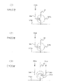
図5(1)に示すようにプリチャージ回路201のTFT202(図1参照)は、nチャネル型(NMOS型)のTFT202aから構成されてもよいし、図5(2)に示すようにpチャネル型(PMOS型)のTFT202bから構成されてもよいし、図5(3)に示すようにnチャネル及びpチャネルの相補型MOS型(CMOS型)のTFT202cから構成されてもよい。尚、図5(1)から図5(3)において、図1に示したプリチャージ回路駆動信号線206を介して入力されるプリチャージ回路駆動信号206a、206bは、ゲート電圧として各TFT202a〜202cに入力される。同じく図1に示したプリチャージ信号線204を介して入力されるプリチャージ信号206a、206bは、ソース電圧として各TFT202a〜202cに入力される。nチャネル型のTFT202aにゲート電圧として印加されるプリチャージ回路駆動信号206aと、pチャネル型のTFT202bにゲート電圧として印加されるプリチャージ回路駆動信号206bとは、相互に反転信号である。従って、プリチャージ回路201をCMOS型のTFT202cで構成する場合には、プリチャージ回路駆動信号線206が少なくとも2本以上必要となる。或いは、例えば、TFT202cの手前でプリチャージ回路駆動信号206aをインバータ回路により反転させて、プリチャージ回路駆動信号206bを形成してもよい。
【0046】
図6(1)に示すようにサンプリング回路301のTFT302(図1参照)は、nチャネル型のTFT302aから構成されてもよいし、図6(2)に示すようにpチャネル型のTFT302bから構成されてもよいし、図6(3)に示すようにCMOS型のTFT302cから構成されてもよい。尚、図6(1)から図6(3)において、図1に示した画像入力信号線VIDn(VID1〜VID6)を介して入力される6つの画像信号は、ソース電圧として各TFT302a〜302cに入力される。同じく図1に示したデータ線駆動回路101からサンプリング回路駆動信号線306を介して入力されるサンプリング回路駆動信号306a、306bは、ゲート電圧として各TFT302a〜302cに入力される。また、サンプリング回路301においても、前述のプリチャージ回路201の場合と同様に、nチャネル型のTFT302aにゲート電圧として印加されるサンプリング回路駆動信号306aと、pチャネル型のTFT302bにゲート電圧として印加されるサンプリング回路駆動信号306bとは、相互に反転信号である。従って、サンプリング回路301をCMOS型のTFT302cで構成する場合には、サンプリング回路駆動信号306a、306b用のサンプリング回路駆動信号線306が2本必要となる。
【0047】
尚、以上説明した実施の形態では、サンプリング回路301は、隣接する6本のデータ線35に対して、6相展開された画像信号をサンプリングした後に同時に印加し、更にこのような画像信号の印加を6本のデータ線35からなるグループ毎に順次行うように構成したが、この相展開の数及び同時に印加するデータ線の数は、6に限られない。例えば、当該サンプリング回路301におけるサンプリング能力が高ければ、1本のデータ線35に対して順次に、相展開されていない画像信号を供給するように構成してもよいし、若しくは、3本、12本、24本等のデータ線に対して3相展開、12相展開、24相展開等された画像信号を供給するように構成してもよい。尚、この数としては、カラー画像信号が3つの色(赤、青、黄)に係る信号からなることとの関係から、3の倍数であると、NTSC表示やPAL表示等のビデオ表示をする際に制御や回路を簡易化する上で好ましい。また、少なくとも画像信号の相展開数分だけ、画像入力信号線が必要であることは言うまでもない。
【0048】
(液晶パネルの構成)
次に、液晶装置200が含む液晶パネル部分の具体的構成について図7及び図8を参照して説明する。ここに、図7はTFTアレイ基板上のTFT素子の断面図であり、図8は図7に示したTFTアレイ基板上の画面表示領域を形成する隣接した画素群の平面図である。尚、図7においては、各層や各部材を図面上で認識可能な程度の大きさとするため、各層や各部材毎に縮尺を異ならしめてある。
【0049】
図7の断面図において、液晶パネル10は、各画素に設けられるTFT30部分において、TFTアレイ基板1並びにその上に積層された第1層間絶縁層41、半導体層32、ゲート絶縁層33、走査線31(ゲート電極)、第2層間絶縁層42、データ線35(ソース電極)、第3層間絶縁層43、画素電極11及び配向膜12を備えている。液晶パネル10はまた、例えばガラス基板から成る対向基板2並びにその上に積層された共通電極21、配向膜22及びブラックマトリクス23を備えている。液晶パネル10は更に、これらの両基板間に挟持された液晶層50を備えている。
【0050】
ここでは先ず、これらの層のうち、TFT30を除く各層の構成について順に説明する。
【0051】
TFT30の下地となる第1層間絶縁層41は、10000Å程度の厚みのNSG、PSG、BSG、BPSGなどのシリケートガラス膜、窒化シリコン膜や酸化シリコン膜等からなる。尚、第1層間絶縁層41に対し、約900℃のアニール処理を施すことにより、汚染を防ぐと共に平坦化してもよい。更に、TFTアレイ基板1の表面が鏡面状に研磨され、洗浄等により十分に汚染防止処理がなされている場合には、第1層間絶縁層41を設ける必要が無い。また、第2層間絶縁層42及び第3層間絶縁層43は夫々、5000〜15000Å程度の層みを持つNSG、PSG、BSG、BPSGなどのシリケートガラス膜、窒化シリコン膜や酸化シリコン膜等からなる。
【0052】
画素電極11は例えば、ITO膜(インジウム・ティン・オキサイド膜)などの透明導電性薄膜からなる。このような画素電極11は、スパッタリング処理等によりITO膜等を約500〜2000Åの厚さに堆積した後、フォトリソグラフィ工程、エッチング工程を施すこと等により形成される。尚、当該液晶パネル10を反射型の液晶装置に用いる場合には、Al等の反射率の高い不透明な材料から画素電極11を形成してもよい。
【0053】
配向膜12は例えば、ポリイミド薄膜などの有機薄膜からなる。このような配向膜12は、例えばポリイミド系の塗布液を塗布した後、所定のプレティルト角を持つように且つ所定方向でラビング処理を施すこと等により形成される。
【0054】
共通電極21は、対向基板2の全面に渡って形成されている。このような共通電極21は、例えばスパッタリング処理等によりITO膜等の透明性導電膜を約500〜2000Åの厚さに堆積して形成される。
【0055】
配向膜22は、例えば、ポリイミド薄膜などの有機薄膜からなる。このような配向膜22は、例えばポリイミド系の塗布液を塗布した後、所定のプレティルト角を持つように且つ所定方向でラビング処理を施すこと等により形成される。
【0056】
ブラックマトリクス23は、TFT30に対向する所定領域に設けられている。このようなブラックマトリクス23は、前述の周辺見切り53同様に、Cr、Ni、Alなどの金属材料を用いたスパッタリング、フォトリソグラフィ及びエッチングにより形成されたり、カーボンやTiをフォトレジストに分散した樹脂ブラックなどの材料から形成される。ブラックマトリクス23は、TFT30の半導体層32の少なくともチャネル領域に対する遮光の他に、コントラストの向上、色材の混色防止などの機能を有する。
【0057】
液晶層50は、画素電極11と共通電極21とが対面するように配置されたTFTアレイ基板1と対向基板2との間において、シール材52(図3及び図4参照)により囲まれた空間に液晶が真空吸引等により封入されることにより形成される。液晶層50は、画素電極11からの電界が印加されていない状態で配向膜12及び22により所定の配向状態を採る。液晶層50は、例えば一種又は数種類のネマティック液晶を混合した液晶からなる。シール材52は、二つの基板1及び2をそれらの周辺で貼り合わせるための、例えば光硬化性樹脂や熱硬化性樹脂からなる接着剤であり、両基板間の距離を所定値とするためのスペーサが混入されている。
【0058】
次に、TFT30に係る各層の構成について順に説明する。
【0059】
TFT30は、走査線31(ゲート電極)、走査線31からの電界によりチャネルが形成されるポリシリコン膜等からなる半導体層32、走査線31と半導体層32とを絶縁するゲート絶縁層33、半導体層32に形成されたソース領域34、データ線35(ソース電極)、及び半導体層32に形成されたドレイン領域36を備えている。ドレイン領域36には、複数の画素電極11のうちの対応する一つが接続されている。ソース領域34及びドレイン領域36は後述のように、半導体層32に対し、n型又はp型のチャネルを形成するかに応じて所定濃度のn型用又はp型用のドーパントをドープすることにより形成されている。n型チャネルのTFTは、動作速度が速いという利点があり、画素のスイッチング素子として好適である。
【0060】
TFT30を構成する半導体層32は、例えば、下地としての第1層間絶縁層41上にa−Si(アモルファスシリコン)膜を形成後、アニール処理を施して約500〜2000Åの厚さに固相成長させることにより形成する。この際、nチャネル型のTFT30の場合には、Sb(アンチモン)、As(砒素)、P(リン)などのV族元素のドーパントを用いたイオン注入等によりドープする。また、pチャネル型のTFT30の場合には、Al(アルミニウム)、B(ボロン)、Ga(ガリウム)、In(インジウム)などのIII族元素のドーパントを用いたイオン注入等によりドープする。特にTFT30をLDD(LightlyDoped Drain)構造を持つnチャネル型のTFTとする場合、半導体層32に、ソース領域34及びドレイン領域36のうちチャネル側に夫々隣接する一部にPなどのV族元素のドーパントにより低濃度ドープ領域を形成し、同じくPなどのV族元素のドーパントにより高濃度ドープ領域を形成する。また、pチャネル型のTFT30とする場合、半導体層32に、 BなどのIII族元素のドーパントを用いてソース領域34及びドレイン領域36を形成する。このようにLDD構造とした場合、ショートチャネル効果を低減できる利点が得られる。尚、TFT30は、低濃度ドープ領域に不純物イオンをドーパントしないオフセット構造のTFTとしてもよいし、ゲート電極31をマスクとして高濃度の不純物イオンをドーパントすることにより自己整合的にソース・ドレイン領域を形成するセルフアライン型のTFTとしてもよい。
【0061】
ゲート絶縁層33は、半導体層32を約900〜1300℃の温度により熱酸化することにより、300〜1500Å程度の比較的薄い厚さの熱酸化膜を形成して得る。
【0062】
走査線31(ゲート電極)は、減圧CVD法等によりポリシリコン膜を堆積した後、ゲートマスクを用いたフォトリソグラフィ工程、エッチング工程等により形成される。或いは、W(タングステン)やMo(モリブデン)等の金属膜又は金属シリサイド膜から形成されてもよい。この場合、走査線31(ゲート電極)を、ブラックマトリクス23が覆う領域の一部又は全部に対応する遮光膜として配置すれば、金属膜や金属シリサイド膜の持つ遮光性により、ブラックマトリクス23の一部又は全部を省略することも可能となる。この場合特に、対向基板2とTFTアレイ基板1との貼り合わせずれによる画素開口率の低下を防ぐことが出来る利点がある。
【0063】
データ線35(ソース電極)は、画素電極11と同様にITO膜等の透明導電性薄膜から形成してもよい。或いは、スパッタリング処理等により、約1000〜7000Åの厚さに堆積されたAl等の低抵抗金属や金属シリサイド等から形成してもよい。
【0064】
また、第2層間絶縁層42には、ソース領域34へ通じるコンタクトホール37及びドレイン領域36へ通じるコンタクトホール38が夫々形成されている。このソース領域34へのコンタクトホール37を介して、データ線35(ソース電極)はソース領域34に電気的接続される。更に、第3層間絶縁層43には、ドレイン領域36へのコンタクトホール38が形成されている。このドレイン領域36へのコンタクトホール38を介して、画素電極11はドレイン領域36に電気的接続される。前述の画素電極11は、このように構成された第3層間絶縁層43の上面に設けられている。各コンタクトホールは、例えば、反応性エッチング、反応性イオンビームエッチング等のドライエッチングにより形成すると、微細加工が可能となる。
【0065】
尚、一般にはチャネルが形成される半導体層32は、光が入射するとポリシリコン膜が有する光電変換効果により光電流が発生してしまいTFT30のトランジスタ特性が劣化するが、本実施の形態では、対向基板2には各TFT30に夫々対向する位置にブラックマトリクス23が形成されているので、入射光が半導体層32に入射することが防止される。更にこれに加えて又は代えて、ゲート電極を上側から覆うようにデータ線35(ソース電極)をAl等の不透明な金属薄膜から形成すれば、ブラックマトリクス23と共に又は単独で、半導体層32の少なくともチャネル領域への入射光(即ち、図7で上側からの光)の照射を効果的に防ぐことが出来る。
【0066】
ここで、図8の平面図に示すように、以上のように構成された画素電極11は、TFTアレイ基板1上にマトリクス状に配列され、各画素電極11に隣接してTFT30が設けられており、また画素電極11の縦横の境界に夫々沿ってデータ線35(ソース電極)及び走査線31(ゲート電極)が設けられている。また、走査線31に沿って容量線31‘が配設されており、画面表示領域の外側に延設され、定電位線501とコンタクトホール502によって電気的に接続される。定電位線501は本来デッドスペースである周辺見切り53下に形成することにより、スペースの有効利用を図るとよい。また、図8に示すようにプリチャージ信号線204やプリチャージ回路駆動信号線206を周辺見切り53下に設けるようにしてもよい。更に、定電位線501はデータ線駆動回路101や走査線駆動回路104の正電位或いは負電位の電源と電気的に接続してもよいし、実装端子102から専用配線を設けて、自由に電位を設定してもよいことは言うまでもない。ところで、本実施の形態では、画素スイッチング用のTFT30を単一のゲート電極31で制御するシングルゲート構造を有するタイプの画素を示したが、同一の走査信号が供給される複数のゲート電極31をTFT30のソース・ドレイン間に設けてもよい。このような構成を採れば、TFT30のチャネル領域とドレイン領域の接合部におけるリーク電流を低減することができる。尚、図8は、説明の都合上、画素電極11のマトリクス状配列等を簡略化して示すためのものであり、実際の各電極は層間絶縁層の間や上をコンタクトホール等を介して配線されており、図7から分かるように3次元的により複雑な構成を有している。
【0067】
再び図7において、画素電極11には蓄積容量70が夫々設けられている。この蓄積容量70は、より具体的には、半導体層32と同一工程により形成される第1蓄積容量電極32’、ゲート絶縁層33と同一工程により形成される絶縁層33’、走査線31と同一工程により形成される容量線31’(第2蓄積容量電極)、第2及び第3層間絶縁層42及び43、並びに第2及び第3層間絶縁層42及び43を介して容量線31’に対向する画素電極11の一部から構成されている。このように蓄積容量70が設けられているため、デューティー比が小さくても高精細な表示が可能とされる。
【0068】
図7において、液晶パネル10には、プリチャージ回路201のTFT202(図1参照)がデータ線35毎に設けられている。このTFT202は、より具体的には、半導体層32と同一工程により形成される半導体層32”、ゲート絶縁層33と同一工程により形成されるゲート絶縁層33”及び走査線31(ゲート電極)と同一工程により形成されるプリチャージ回路駆動信号線206(ゲート電極)を備えている。半導体層32”には、TFT30の場合と同様に、ソース領域34”、チャネル形成領域及びドレイン領域36”が設けられ、第2層間絶縁層42に開けられたコンタクトホールを通じてドレイン領域36”にはデータ線35が接続され、ソース領域34”にはプリチャージ信号線204が接続されている。そして、このような層構造を持つTFT202は、対向基板2に設けられた遮光性の周辺見切り53に対向する位置において、TFTアレイ基板1上に設けられている。
【0069】
尚、図7には図示していないが、サンプリング回路301のTFT302(図1参照)は、プリチャージ回路201のTFT202と同様に構成されており、対向基板2に設けられた遮光性の周辺見切り53に対向する位置において、TFTアレイ基板1上に設けられている。
【0070】
本実施の形態では特に、TFT30はp−Si(ポリシリコン)タイプのTFTであるので、TFT30の形成時に同一薄膜形成工程で、サンプリング回路201、プリチャージ回路301、データ線駆動回路101、走査線駆動回路104等の同じくp−SiTFTタイプのTFT202、302等から構成された周辺回路を形成できるので製造上有利である。例えば、データ線駆動回路101及び走査線駆動回路104は、図5(3)及び図6(3)に示したプリチャージ回路201やサンプリング回路301の場合と同様に、nチャネル型p−SiTFT及びpチャネル型p−SiTFTから構成されるCMOS構造の複数のTFTからTFTアレイ基板1上の周辺部分に形成される。
【0071】
尚、図7には示されていないが、対向基板2の投写光が入射する側及びTFTアレイ基板1の投写光が出射する側には夫々、例えば、TN(ツイステッドネマティック)モード、 STN(スーパーTN)モード、D−STN(ダブル−STN)モード等の動作モードや、ノーマリーホワイトモード/ノーマリーブラックモードの別に応じて、偏光フィルム、位相差フィルム、偏光板などが所定の方向で配置される。
【0072】
以上説明した液晶パネル10は、カラー液晶プロジェクタに適用されるため、3つの液晶パネル10がRGB用のライトバルブとして夫々用いられ、各パネルには夫々RGB色分解用のダイクロイックミラーを介して分解された各色の光が入射光として夫々入射されることになる。従って、各実施の形態では、対向基板2に、カラーフィルタは設けられていない。しかしながら、液晶パネル10においてもブラックマトリックス23の形成されていない画素電極11に対向する所定領域にRGBのカラーフィルタをその保護膜と共に、対向基板2上に形成してもよい。このようにすれば、液晶プロジェクタ以外の直視型や反射型のカラー液晶テレビなどのカラー液晶装置に本実施の形態の液晶パネルを適用できる。
【0073】
更に、対向基板2上に1画素1個対応するようにマイクロレンズを形成してもよい。このようにすれば、入射光の集光効率を向上することで、明るい液晶パネルが実現できる。更にまた、対向基板2上に、何層もの屈折率の相違する干渉層を堆積することで、光の干渉を利用して、RGB色を作り出すダイクロイックフィルタを形成してもよい。このダイクロイックフィルタ付き対向基板によれば、より明るいカラー液晶パネルが実現できる。
【0074】
液晶パネル10において、TFTアレイ基板1側における液晶分子の配向不良を抑制するために、第3層間絶縁層43の上に更に平坦化膜をスピンコート等で塗布してもよく、又はCMP処理を施してもよい。若しくは、第3層間絶縁層43自体を平坦化膜にしてもよい。
【0075】
また、液晶パネル10のスイッチング素子は、正スタガ型又はコプラナー型のp−SiTFTであるとして説明したが、逆スタガ型のTFTやa−SiTFT等の他の形式のTFTに対しても、本実施の形態は有効である。
【0076】
更に、液晶パネル10においては、一例として液晶層50をネマティック液晶から構成したが、液晶を高分子中に微小粒として分散させた高分子分散型液晶を用いれば、配向膜12及び22、並びに前述の偏光フィルム、偏光板等が不要となり、光利用効率が高まることによる液晶パネルの高輝度化や低消費電力化の利点が得られる。更に、画素電極11をAl等の反射率の高い金属膜から構成することにより、液晶パネル10を反射型液晶装置に適用する場合には、電圧無印加状態で液晶分子がほぼ垂直配向されたSH(スーパーホメオトロピック)型液晶などを用いても良い。更にまた、液晶パネル10においては、液晶層50に対し垂直な電界(縦電界)を印加するように対向基板2の側に共通電極21を設けているが、液晶層50に平行な電界(横電界)を印加するように一対の横電界発生用の電極から画素電極11を夫々構成する(即ち、対向基板2の側には縦電界発生用の電極を設けることなく、TFTアレイ基板1の側に横電界発生用の電極を設ける)ことも可能である。このように横電界を用いると、縦電界を用いた場合よりも視野角を広げる上で有利である。その他、各種の液晶材料(液晶相)、動作モード、液晶配列、駆動方法等に本実施の形態を適用することが可能である。
【0077】
(サンプリング回路及びプリチャージ回路)
ここで、本実施の形態に係るサンプリング回路及びプリチャージ回路について、図9から図13を参照して更に詳しく説明する。
【0078】
図9(a)の平面図に示すように、サンプリング回路301は、画像入力信号線VIDn(n=1〜6)、サンプリング回路駆動信号線306及びデータ線35が平行に配置されている。画像入力信号線VIDn(n=1〜6)は、各コンタクトホール37a”を介して各TFT302のソース領域に電気的接続されており、データ線35は各コンタクトホール38a”を介して各TFT302のドレイン領域に電気的接続されている。また、サンプリング回路駆動信号線306はTFT302のゲート電極として、これらのソース領域とドレイン領域とを結ぶチャネル部分にゲート絶縁膜を介して対向配置されている。
【0079】
図9(b)のA−A’断面図に示すように、 TFT302はLDD構造を有し、半導体層中において、サンプリング回路駆動信号線306(ゲート電極)と同じ長さを持つチャネルの両脇に低濃度ドープ領域(LDD)領域32a”が設けられており、その更に両脇に高濃度ドープ領域が設けられている。
【0080】
本実施の形態では特に、図9(a)の平面図及び図9(b)のA−A’断面図に示すように、TFT302のゲート長をLAとし、LDD長をLDDAとする。これらの長さは、後述のように最適化されている。尚、TFT302は、オフセット構造のTFTとしてもよいし、セルフアライン型のTFTとしてもよい。
【0081】
図10(a)の平面図に示すように、プリチャージ回路201は、プリチャージ信号線204、プリチャージ回路駆動信号線206及びデータ線35が平行に配置されている。プリチャージ信号線204は、各コンタクトホール37b”を介して各TFT202のソース領域に電気的接続されており、データ線35は各コンタクトホール38b”を介して各TFT202のドレイン領域に電気的接続されている。また、プリチャージ回路駆動信号線206はTFT202のゲート電極として、これらのソース領域とドレイン領域とを結ぶチャネル部分にゲート絶縁膜を介して対向配置されている。
【0082】
図10(b)のB−B’断面図に示すように、TFT202はLDD構造を有し、p−Si層中において、プリチャージ回路駆動信号線206(ゲート電極)と同じ長さを持つチャネルの両脇に低濃度ドープ領域(LDD)領域32b”が設けられており、その更に両脇に高濃度ドープ領域が設けられている。
【0083】
本実施の形態では特に、図10(a)の平面図及び図10(b)のB−B’断面図に示すように、TFT202のゲート長をLBとし、LDD長をLDDBとする。これらの長さは、後述のように最適化されている。尚、TFT202は、オフセット構造のTFTとしてもよいし、セルフアライン型のTFTとしてもよい。
【0084】
ここで図11の表1を参照して、サンプリング回路301及びプリチャージ回路201により画素電極11に画像信号及びプリチャージ信号を夫々書込む際の各TFT302及び202の電流供給能力について検討する。ここに、TFTの電流供給能力とは、オンされた状態のTFTが、ソース及びドレイン間にかかる所定電圧に応じてそれらの間にあるチャネルを介して供給できる電流量(単位は、例えばアンペア)であり、単位時間当りにチャネルを介して供給可能な電荷量(単位は、例えばクーロン/秒)に等しい。この電流量(電荷量)は、適当な動作条件下で、TFTのオン抵抗(単位は、例えばΩ)にほぼ反比例したり(即ち、オン導電率に比例したり)、TFTのサイズを規定するチャネル長等を固定した際のチャネル幅(単位は、例えばメートル)にほぼ比例したり、TFTのサイズを規定するチャネル幅等を固定した際のTFTのチャネル長(単位は、例えばメートル)にほぼ反比例したりする性質を持つものである。
【0085】
図11に示した表1は、TFT特性パラメータとしてソース−ドレイン間のオン状態における抵抗R(Ω)が異なる各種TFTにおける時定数τ(sec)の値、T/τの値、EXP(−T/τ)の値、立ち上がり(%)及び不足電圧(mV)を夫々示したものである。ここでは全てのTFTについて、書込み期間を1.00E−07(sec)に設定し、書込み電圧を10(V)に設定して、ソース−ドレイン間の容量C(F)を2.00E−11(F)に設定してある。但し、Tは、ゲートに加えられる駆動信号のパルス幅に相当する各TFTがオンされる時間である。立ち上がり(%)としては、各時間Tの間にドレイン又はソースに接続された画素電極の電圧がどれだけ立ち上がったかを、飽和状態(完全に立ち上がった状態)を100%として百分率で示してある。また、不足電圧(mV)としては、各立ち上がりに応じて、書込み電圧に対してソース−ドレインを介して供給された電荷により実際に画素電極に書込まれた電圧がどれだけ不足しているかをこれらの電圧の差として示してある。
【0086】
この表1から分かるように、例えばTFTのチャネル長を短く或いはチャネル幅を広くとることによって、TFTのオン抵抗Rを低くすればする程、容量一定の条件下で時定数τ(sec)を小さく出来、更に書込み電圧一定の条件下でオン電流が増加することにより十分に画素電極の電圧が立ち上がり、この結果として不足電圧が少なくなる。より一般には、単位時間当りにTFTが供給可能な電荷を示すTFTの電流供給能力が大きくなる程、不足電圧は少なくなる。
【0087】
このように一般に、TFTにおいては電流供給能力が異なれば不足電圧状況が異なるので、本実施の形態の構成においても、サンプリング回路301のTFT302の電流供給能力をどのように設定するかにより、この設定に依存する不足電圧を補うためにプリチャージするプリチャージ回路201のTFT202に必要な電流供給能力が決まってくる。そこで、本実施の形態では、図9及び図10に夫々示したサンプリング回路301のTFT302の電流供給能力と、プリチャージするプリチャージ回路201のTFT202に必要な電流供給能力との最適化を以下のように行う。
【0088】
即ち、サンプリング回路301により画素電極に画像信号を書込むのに必要な時間は、各画素電極11における液晶部分に液晶印加電圧が印加される周波数であるドット周波数と、画像信号をサンプリング回路301に供給するデータ線駆動回路101(シフトレジスタ等)の系列数及び方式とに依存する。ここで、本実施の形態に適用可能な各種の表示モードとして、VGA方式、SVGA方式、XGA方式及びEWS方式等があるが、これらの方式についてのドット周波数、水平周波数、水平帰線期間、プリチャージ時間及び画像選択時間を図12の表2に示す。尚、ここでは、垂直周波数は全て約60kHzに設定してあり、水平帰線期間でプリチャージを行うことを想定している。また、画像選択時間は、サンプリング回路301が、データ線35を順次駆動する場合並びに6本、12本及び24本ずつ同時に駆動する場合について夫々示してある。
【0089】
図12に示す表2において、例えばドット周波数が65MHzと比較的高いXGA方式においてデータ線35を12本同時に駆動する場合には、サンプリング回路301により一つの画素電極11に画像信号としての電荷を書込むのに必要な時間は、180nsecの画像選択時間に対し若干のマージンを見て(前後の画像信号を書込むことにより生じるゴースト現象を防止するため)約150nsec(ナノ秒)となる。これに対して、例えば水平帰線期間に全てのデータ線35を同時にプリチャージする場合に、プリチャージ信号としての電荷を書込むのに必要な時間は、当該水平帰線期間約4μsec(マイクロ秒)に対し、画像信号の極性反転時の遅延やプリチャージ回路駆動信号の遅延等を考慮して、若干のマージンを見ると、約2μsecとなる。
【0090】
従ってこの場合には、本願発明者らの考察によれば、プリチャージ回路201のTFT202の電流供給能力A2は、サンプリング回路301のTFT302の電流供給能力A1の1/10程度で十分であると考えられる。同様の考え方で、図12の表2に示したVGA方式、SVGA方式、XGA方式及びEWS方式の夫々について、サンプリング回301路のオン電流に対する、十分にプリチャージするために必要なプリチャージ回路201のオン電流の比(即ち、オン電流比)を図13の表3に示す。この場合、TFTのソース−ドレイン間に、同電圧を印加した時のオン電流比を示してある。従って、この印加電圧を変化させると、これらのオン電流比は変化する。
【0091】
図13に示す表3によれば、十分にプリチャージするために必要なオン電流比は、表示モード及び駆動方式に依存している。即ち、十分にプリチャージするために必要なプリチャージ回路201のTFT202の電流供給能力A2は、表示モード及び駆動方式に依存する。
【0092】
そこで本実施の形態では、データ線35一本に対するサンプリング回路301のTFT302の電流供給能力A1及びプリチャージ回路201のTFT202の電流供給能力A2並びにデータ線35一本に対してサンプリング回路301のTFT302がオンされる時間ΔT1(画像信号を書込む時間)及びプリチャージ回路201のTFT202がオンされる時間ΔT2(プリチャージ信号を書込む時間)との間には、次の式(1)に示される関係が成立するように、TFT202及び302を構成する。
【0093】
(ΔT1/ΔT2)×A1≦A2 ……(1)
ここに、TFTの電流供給能力とは、オンされた状態のTFTが、そのチャネルを介して供給できる電流量であり、単位時間当りに供給可能な電荷量に等しい。従って、このような関係が成立すれば、プリチャージ回路201のTFT202の電流供給能力A2は、サンプリング回路301から供給される画像信号に対してプリチャージの効果を発揮するために必要なレベル以上となる。そして、プリチャージ回路201のTFT202を、必要最低限の電流供給能力A2に対応した必要最低限のサイズを持つように、即ち、(ΔT1/ΔT2)×A1≒A2なる関係が成立するように構成すれば、プリチャージ回路201のTFT202ひいてはプリチャージ回路201全体の占有面積をほぼ限界まで小さくできる。
【0094】
以上の結果、サンプリング機能及びプリチャージ機能を、ドット周波数やデータ線駆動回路101の系列数や方式に応じて、必要最低限度の電流供給能力や必用最低限度のTFTサイズにより夫々実現するサンプリング回路301及びプリチャージ回路201が得られる。即ち、ドット周波数やデータ線駆動回路101の系列数や方式に対して、サンプリング回路301及びプリチャージ回路201における電流供給能力やTFTサイズの最適化がなされる。
【0095】
ところで図14に示すように、一般にTFTのチャネル長に応じてTFTの立ち上がり特性は変化するため、TFTをスイッチング素子として用いる場合のしきい値電圧はチャネル長に応じて変化する。仮に異なるしきい値電圧のTFTをプリチャージ回路201とサンプリング回路301とで用いると、ゲート遅延によりプリチャージ回路201から供給されるプリチャージ信号とサンプリング回路301から供給される画像信号とのタイミングを合わせるが実践上困難になってしまう。
【0096】
そこで、本実施の形態では特に、図9に示したサンプリング回路301のTFT302のチャネル長LAと図10に示したプリチャージ回路201のTFT202のチャネル長LBとは、これらのTFT302及び202のしきい値電圧の差が所定の微小値未満となる程度に相等しくされている。このような所定の微小値は、サンプリング回路301とプリチャージ回路201とにおけるチャネル長LA及びLBの差に起因したTFT特性の相違に基づくゲート遅延による当該液晶装置200の表示画像への悪影響が視認不可能な範囲に収まるように、チャネル長LA及びLBを徐々に変化させてその影響を見たり計算したりする実験、理論演算、シミュレーション等により予め定められる。
【0097】
このようにチャネル長LAとチャネル長LBとは、ほぼ同じ長さとされるが、このとき本実施の形態では更に、図9(a)に示したサンプリング回路301のTFT302のチャネル幅WAと、図10(a)に示したプリチャージ回路201のTFT202のチャネル幅WBとの間には、次の式(2)に示される関係が成立するように、TFT202及び302を構成する。
【0098】
(ΔT1/ΔT2)×WA≦WB ……(2)
このような関係が成立すれば、チャネル幅WBにほぼ比例するプリチャージ回路201のTFT202の電流供給能力A2は、サンプリング回路301から供給される画像信号に対してプリチャージの効果を発揮するために必要なレベル以上となる。そして、プリチャージ回路201のTFT202を、必要最低限のチャネル幅WBを持つように、即ち、(ΔT1/ΔT2)×WA≒WBなる関係が成立するように構成すれば、プリチャージ回路201のTFT202ひいてはプリチャージ回路201全体の占有面積をほぼ限界まで小さくできる。この結果、サンプリング機能及びプリチャージ機能を、ドット周波数やデータ線駆動回路101の系列数や方式に応じて、必要最低限度のチャネル幅WA及びWBにより夫々実現するサンプリング回路201及びプリチャージ回路301が得られる。即ち、サンプリング回路301及びプリチャージ回路201におけるTFTチャネル幅の最適化がなされる。
【0099】
前述のようにTFT202及び203は、オフ時にドレイン電極−ソース電極間に保持された保持電圧がチャネルを介してリークするため、チャネル長を短くするのには一定の制限が課せられるが、本実施の形態によれば、チャネル長LA及びLBを適当な長さでほぼ同じにしておき、プリチャージ回路201のTFT202のチャネル幅WBをほぼ限界まで小さく出来る。
【0100】
更に本実施の形態では、図9(b)及び図10(b)に示したように、TFT202及び302は、夫々LDD構造を持つが、これらのLDD長LDDA及びLDDBとは、上述のチャネル長LA及びLBの場合と同様に、ほぼ等しくされている。そして、このとき特に、サンプリング回路301のTFT302のチャネル幅WA(図9(a)参照)と、プリチャージ回路201のTFT202のチャネル幅WB(図10(a)参照)との間に、前述の式(2)に示される関係が成立するようにTFT302及び202は構成されているので、チャネル幅WBにほぼ比例する、TFT202の電流供給能力A2は、サンプリング回路301から供給される画像信号に対してプリチャージの効果を発揮するために必要なレベル以上となる。この結果、サンプリング回路301及びプリチャージ回路201におけるLDD構造を持つTFTについてのチャネル幅の最適化がなされる。尚、TFT202及び302は夫々、オフセット構造のTFTとしてもよいし、セルフアライン型のTFTとしてもよいことは言うまでもない。
【0101】
以上の実施の形態では、プリチャージ回路201が、プリチャージ信号を画像信号の水平帰線期間に、複数のデータ線に対し同時に供給するように構成されている。この場合、プリチャージ回路201には、複数のデータ線35に対応する比較的高い電流供給能力A2が必要となるが、前述の式(1)或いは(2)に示される関係が成立するようにTFT202及び302は夫々構成されているので、この電流供給能力A2は、プリチャージの効果を発揮するために必要なレベル以上となる。但し、このようにプリチャージ信号を水平帰線期間に同時に供給しなくても、上述した本願独自の電流供給能力及びTFTサイズの最適化という効果は得られる。例えば、サンプリング回路301のTFT302は、データ線駆動回路101が有するシフトレジスタから順次供給される転送信号により夫々(例えば、1本ずつ順次に若しくは3本、6本、12本、24本等ずつ同時に順次に)オンされて、画像信号を転送信号の周期で複数のデータ線35に夫々供給し、且つプリチャージ回路201のTFT202は、転送信号により夫々オンされて、プリチャージ信号を転送信号の周期に対応する期間だけ画像信号に先行して複数のデータ線35に夫々順次供給するように構成してもよい。この場合には、プリチャージ回路201には、各データ線35に対応する比較的低い電流供給能力A2が必要となるが、前述の式(1)或いは(2)に示される関係が成立するようにTFT202及び302は夫々構成されているので、やはり、この電流供給能力A2は、プリチャージの効果を発揮するために必要なレベル以上となる。このように構成すると、プリチャージ回路201の構成が若干複雑になるが電荷供給のための負荷が軽減される利点が得られる。
【0102】
(液晶装置の動作)
次に、以上のように構成された液晶装置200の動作について図1及び図2を参照して説明する。
【0103】
先ず、走査線駆動回路104は、所定タイミングで走査線31に走査信号をパルス的に線順次で印加する。
【0104】
これと並行して、例えば6つの画像入力信号線VID1〜VID6から6つのパラレルな画像信号を受けると、サンプリング回路301は、これらの画像信号をサンプリングする。データ線駆動回路101は、走査線駆動回路104がゲート電圧を印加するタイミングに合わせて、6本の画像入力信号線VID1〜VID6夫々について一つのデータ線毎にサンプリング回路駆動信号を供給して、サンプリング回路301のTFT302をオン状態とする。これにより、隣接する6本のデータ線35に対して、サンプリング回路301にサンプリングされた画像信号を同時に印加し、更にこのような画像信号の印加を6本のデータ線35からなるグループ毎に順次行う。即ち、データ線駆動回路101とサンプリング回路301により、6相展開されて画像入力信号線VID1〜VID6から入力された6つのパラレルな画像信号は、データ線35に供給される。
【0105】
他方で、各画像信号に先行するタイミングで、プリチャージ回路201は、プリチャージ信号を各データ線35に供給する。より具体的には、プリチャージ回路201は、プリチャージ信号(NRS)をデータ線35に書込むための電源をプリチャージ信号線206から受けつつ、プリチャージ回路駆動信号線206を介して入力されるプリチャージ回路駆動信号(NRG)に応じてTFT202をオン状態とし、プリチャージ信号(NRS)をデータ線35に書込む(図2参照)。
【0106】
このように、走査信号(ゲート電圧)及び画像信号(ソース電圧)の両方が印加されたTFT30においては、ソース領域34、半導体層32に形成されたチャネル及びドレイン領域36を介して画素電極11に電圧が印加される。そして、この画素電極11の電圧は、ソース電圧が印加された時間よりも例えば3桁も長い時間だけ蓄積容量70(図7参照)により維持される。特に本実施の形態では、液晶を交流駆動するために、1フィールド或いは1フレームといった所定周期毎にソース電圧の電圧極性が反転されるが、上述のように各画像信号がTFT30に供給される前に、各データ線35には、好ましくは中間階調レベルの画素データに相当するプリチャージ信号が供給されているので、画像信号を書込む際の負荷は軽減されており、データ線35の電位レベルは、前回に印加された電圧レベルによらずに安定している。このため、今回の画像信号を各データ線35(ソース電極)に安定した電位により供給することができる。
【0107】
以上のように、画素電極11に電圧が印加されると、液晶層50におけるこの画素電極11と共通電極21とに挟まれた部分における液晶の配向状態が変化し、ノーマリーホワイトモードであれば、印加された電圧に応じて入射光がこの液晶部分を通過不可能とされ、ノーマリーブラックモードであれば、印加された電圧に応じて入射光がこの液晶部分を通過可能とされ、全体として液晶パネル10からは画像信号に応じたコントラストを持つ光が出射する。この際、本実施の形態では特に、多相展開された画像信号をサンプリング回路301によりサンプリングし、データ線35に供給するので、高周波数の画像信号を各データ線に所定のタイミングで安定的に走査信号と同期して供給できる。更に、プリチャージ回路201から画像信号に先行してプリチャージ信号が供給されているので、コントラスト比の向上、データ線35の電位レベルの安定、表示画面上のラインむらの低減等が図られ、液晶パネル10の画面表示領域には、高品位の画像が表示される。
【0108】
以上説明した液晶装置においては、データ線駆動回路101及び走査線駆動回路104をTFTアレイ基板1の上に設ける代わりに、例えばTAB(テープオートメイテッドボンディング基板)上に実装された駆動用LSIに、TFTアレイ基板1の周辺部に設けられた異方性導電フィルムを介して電気的及び機械的に接続するようにしてもよい。また、サンプリング回路201、プリチャージ回路301及び検査回路のうちのいずれか一つのみを周辺見切り53下に形成し、残りをTFTアレイ基板1上の周辺部分に形成してもよいし、或いは周辺見切り53の下のスペースを利用せずに、これら全ての回路をTFTアレイ基板1上の周辺部分に形成してもよい。
【0109】
更にまた、以上の実施の形態において、特開平9−127497号公報、特公平3−52611号公報、特開平3−125123号公報、特開平8−171101号公報等に開示されているように、TFTアレイ基板1上においてTFT30に対向する位置(即ち、TFT30の少なくともチャネル領域下側)にも、例えば高融点金属からなる遮光層を設けてもよい。このようにTFT30の下側にも遮光層を設ければ、TFTアレイ基板1の側からの戻り光等がTFT30に入射するのを未然に防ぐことができる。
【0110】
(電子機器)
次に、以上詳細に説明した液晶装置200を備えた電子機器の実施の形態について図15から図19を参照して説明する。
【0111】
先ず図15に、このように液晶装置200を備えた電子機器の概略構成を示す。
【0112】
図15において、電子機器は、表示情報出力源1000、表示情報処理回路1002、前述の走査線駆動回路104及びデータ線駆動回路101を含む駆動回路1004、前述のように周辺見切り下にプリチャージ回路及びサンプリング回路が設けられた液晶パネル10、クロック発生回路1008並びに電源回路1010を備えて構成されている。表示情報出力源1000は、ROM(Read Only Memory)、RAM(Random Access Memory)、光ディスク装置などのメモリ、同調回路等を含み、クロック発生回路1008からのクロック信号に基づいて、所定フォーマットの画像信号などの表示情報を表示情報処理回路1002に出力する。表示情報処理回路1002は、増幅・極性反転回路、相展開回路、ローテーション回路、ガンマ補正回路、クランプ回路等の周知の各種処理回路を含んで構成されており、クロック信号に基づいて入力された表示情報からデジタル信号を順次生成し、クロック信号CLKと共に駆動回路1004に出力する。駆動回路1004は、走査線駆動回路104及びデータ線駆動回路101によって前述の駆動方法により液晶パネル10を駆動する。電源回路1010は、上述の各回路に所定電源を供給する。尚、液晶パネル10を構成するTFTアレイ基板の上に、駆動回路1004を搭載してもよく、これに加えて表示情報処理回路1002を搭載してもよい。
【0113】
次に図16から図19に、このように構成された電子機器の具体例を夫々示す。
【0114】
図16において、電子機器の一例たる液晶プロジェクタ1100は、上述した駆動回路1004がTFTアレイ基板上に搭載された液晶パネル10を含む液晶表示モジュールを3個用意し、夫々RGB用のライトバルブ10R、10G及び10Bとして用いた投写型プロジェクタとして構成されている。液晶プロジェクタ1100では、白色光源のランプユニット1102から投写光が発せられると、ライトガイド1104の内部で、複数のミラー1106を介して、2枚のダイクロイックミラー1108によって、RGBの3原色に対応する光成分R、G、Bに分けられ、各色に対応するライトバルブ10R、10G及び10Bに夫々導かれる。そして、ライトバルブ10R、10G及び10Bにより夫々変調された3原色に対応する光成分は、ダイクロイックプリズム1112により再度合成された後、投写レンズ1114を介してスクリーンなどにカラー画像として投写される。
【0115】
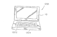
図17において、電子機器の他の例たるラップトップ型のパーソナルコンピュータ1200は、上述した液晶パネル10がトップカバーケース内に備えられており、更にCPU、メモリ、モデム等を収容すると共にキーボード1202が組み込まれた本体1204を備えている。
【0116】
図18において、電子機器の他の例たるページャ1300は、金属フレーム1302内に前述の駆動回路1004がTFTアレイ基板上に搭載されて液晶表示モジュールをなす液晶パネル10が、バックライト1306aを含むライトガイド1306、回路基板1308、第1及び第2のシールド板1310及び1312、二つの弾性導電体1314及び1316、並びにフィルムキャリアテープ1318と共に収容されている。この例の場合、前述の表示情報処理回路1002(図15参照)は、回路基板1308に搭載してもよく、液晶パネル10のTFTアレイ基板上に搭載してもよい。更に、前述の駆動回路1004を回路基板1308上に搭載することも可能である。
【0117】
尚、図18に示す例はページャであるので、回路基板1308等が設けられている。しかしながら、駆動回路1004や更に表示情報処理回路1002を搭載して液晶表示モジュールをなす液晶パネル10の場合には、金属フレーム1302内に液晶パネル10を固定したものを液晶装置として、或いはこれに加えてライトガイド1306を組み込んだバックライト式の液晶装置として、生産、販売、使用等することも可能である。
【0118】
また図19に示すように、駆動回路1004や表示情報処理回路1002を搭載しない液晶パネル10の場合には、駆動回路1004や表示情報処理回路1002を含むIC1324がポリイミドテープ1322上に実装されたTCP(Tape Carrier Package)1320に、TFTアレイ基板1の周辺部に設けられた異方性導電フィルムを介して物理的且つ電気的に接続して、液晶装置として、生産、販売、使用等することも可能である。
【0119】
以上図16から図19を参照して説明した電子機器の他にも、液晶テレビ、ビューファインダ型又はモニタ直視型のビデオテープレコーダ、カーナビゲーション装置、電子手帳、電卓、ワードプロセッサ、ワークステーション、携帯電話、テレビ電話、POS端末、タッチパネルを備えた装置等などが図15に示した電子機器の例として挙げられる。
【0120】
以上説明したように、本実施の形態によれば、相対的に画面表示領域が大きく且つ高品位の画像表示が可能な液晶装置200を備えた各種の電子機器を実現できる。
【0121】
【発明の効果】
以上詳細に説明したように本発明の液晶装置によれば、サンプリング機能及びプリチャージ機能を、ドット周波数やデータ線駆動回路の系列数や方式に応じて、必要最低限度の電流供給能力や必用最低限度のTFTサイズにより夫々実現するサンプリング回路及びプリチャージ回路を得ることが可能となる。更に、このようにTFTサイズを小さく抑えれば、ゲート容量の大きさに依存するプリチャージの遅延をも最小限度に抑えることができ、より正確なタイミングでサンプリングやプリチャージを行うことも可能となる。このように、本願発明により、サンプリング回路及びプリチャージ回路における電流供給能力やTFTサイズの最適化が図られ、液晶パネルや液晶表示モジュールのサイズと比較して相対的に有効表示面積を大きくでき、同時に、より高品位の画像を表示することも可能となる。
【0122】
また、本発明の液晶装置によれば、サンプリング機能及びプリチャージ機能を、ドット周波数やデータ線駆動回路の系列数や方式に応じて、必要最低限度のチャネル幅により夫々実現するサンプリング回路及びプリチャージ回路を得ることが可能となる。更に、このようにチャネル幅を小さく抑えれば、ゲート容量の大きさに依存するプリチャージの遅延をも最小限度に抑えることができ、より正確なタイミングでサンプリングやプリチャージを行うことも可能となる。特に、前述のようにプリチャージ回路の第2TFTは、オフ時に保持電圧がチャネルを介してリークするため、チャネル長を短くするのには一定の制限が課せられるが、本願発明によれば、第1及び第2TFTの間でチャネル長を適当な長さでほぼ同じにしておき、第2TFTのチャネル幅をほぼ限界まで小さく出来るので、該リークの問題にも適切に対処できる。
【図面の簡単な説明】
【図1】 液晶装置の実施の形態におけるTFTアレイ基板上に形成された各種配線、周辺回路等のブロック図である。
【図2】 プリチャージ回路のタイミングチャートである。
【図3】 図1の液晶装置の全体構成を示す平面図である。
【図4】 図1の液晶装置の全体構成を示す断面図である。
【図5】 液晶装置に設けられたプリチャージ回路を構成するTFTの回路図である。
【図6】 液晶装置に設けられたサンプリング回路を構成するTFTの回路図である。
【図7】 液晶装置に備えられた液晶パネルを構成するTFTアレイ基板上のTFT素子示す断面図である。
【図8】 図7の液晶パネルを構成するTFTアレイ基板上の画面表示領域を形成する隣接した画素群の平面図である。
【図9】 液晶装置に設けられたサンプリング回路を各種寸法と共に示す平面図(a)及び断面図(b)である。
【図10】 液晶装置に設けられたプリチャージ回路を各種寸法と共に示す平面図(a)及び断面図(b)である。
【図11】 サンプリング回路を構成する各種TFTにおける不足電圧等を示す表1である。
【図12】 液晶表示駆動に係る各種表示モードにおけるプリチャージ時間、画像選択時間等を示す表2である。
【図13】 図12に示した各種モードにおけるプリチャージ回路とサンプリング回路とのオン電流比を示す表3である。
【図14】 チャネル長を変化させた場合のTFTの立ち上がり特性の変化を示す特性図である。
【図15】 本発明による電子機器の実施の形態の概略構成を示すブロック図である。
【図16】 電子機器の一例としての液晶プロジェクタを示す断面図である。
【図17】 電子機器の他の例としてのパーソナルコンピュータを示す正面図である。
【図18】 電子機器の一例としてのページャを示す分解斜視図である。
【図19】 電子機器の一例としてのTCPを用いた液晶装置を示す斜視図である。
【符号の説明】
1…TFTアレイ基板
2…対向基板
10…液晶パネル
11…画素電極
12…配向膜
21…共通電極
22…配向膜
23…ブラックマトリクス
30…TFT
31…走査線(ゲート電極)
32…半導体層
33…ゲート絶縁層
34…ソース領域
35…データ線(ソース電極)
36…ドレイン領域
37、38…コンタクトホール
41…第1層間絶縁層
42…第2層間絶縁層
43…第3層間絶縁層
50…液晶層
52…シール材
53…周辺見切り
70…蓄積容量
101…データ線駆動回路
102…実装端子
104…走査線駆動回路
200…液晶装置
201…プリチャージ回路
202…TFT
204…プリチャージ信号線
206…プリチャージ回路駆動信号線
301…サンプリング回路
302…TFT[0001]
BACKGROUND OF THE INVENTION
The present invention belongs to the technical field of a matrix driving type liquid crystal device driven by a thin film transistor (hereinafter referred to as TFT) and an electronic device using the same, and in particular, a sampling circuit and a precharge circuit are formed on a TFT array substrate. It belongs to the technical field of liquid crystal devices of the type and electronic equipment using the same.
[0002]
[Prior art]
2. Description of the Related Art Conventionally, in an active matrix driving type liquid crystal device using TFT driving, a large number of pixel electrodes are provided on a TFT array substrate corresponding to a large number of scanning lines and data lines arranged in the vertical and horizontal directions and their intersections. Yes. In addition to these, various peripheral circuits including TFTs such as a sampling circuit, a precharge circuit, a scanning line driving circuit, a data line driving circuit, and an inspection circuit are provided on such a TFT array substrate. There is a case.
[0003]
Among these peripheral circuits, the sampling circuit is a circuit that samples an image signal in order to supply a high-frequency image signal to each data line stably in synchronization with the scanning signal at a predetermined timing. The number of phase expansions of the image signal input to the sampling circuit is determined according to the sampling capability of the sampling circuit. In other words, when the number of pixels in the horizontal direction is fixed, the higher the sampling capacity, the smaller the number of phase developments of the image signal. As a result, the burden imposed on the signal source of the image signal such as the image signal processing circuit in order to perform high-resolution display is reduced by the sampling circuit.
[0004]
The precharge circuit is used to improve the contrast ratio, stabilize the potential level of the data line, reduce line unevenness on the display screen, etc., from the data line driving circuit to the data line driving circuit or directly through the sampling circuit. This is a circuit that reduces the load when the image signal is written to the data line by supplying a precharge signal (image auxiliary signal) at a timing preceding the image signal supplied to. In particular, in the so-called 1H inversion driving method (driving method in which scanning lines are inverted) or the like in which the voltage polarity of the data line that is normally performed to drive the liquid crystal is inverted at a predetermined cycle, the precharge signal is applied to the data line. If the image signal is written in advance, the amount of charge required for writing the image signal to the data line can be remarkably reduced. For example, Japanese Patent Laid-Open No. 7-295520 discloses an example of such a precharge circuit.
[0005]
As described above, by providing peripheral circuits such as a sampling circuit and a precharge circuit on the TFT array substrate, it is possible to display a high-quality image while reducing a burden on hardware resources such as a driving device.
[0006]
[Problems to be solved by the invention]
If the size of the liquid crystal panel and the liquid crystal display module with peripheral circuits added to it is the same, the screen display area defined by the plurality of pixel electrodes arranged in a matrix, that is, the liquid crystal panel is actually aligned. It is said that the larger the area where an image is displayed due to the change, the better as the basic requirement of the display device. Therefore, the peripheral circuit is generally provided in a narrow and narrow peripheral portion of the TFT array substrate located around the screen display area.
[0007]
However, if the above-described sampling circuit and precharge circuit are simply provided in the narrow and long peripheral portion of such a TFT array substrate without any ingenuity, the space for providing the essential scanning line driving circuit, data line driving circuit, etc. However, there is a problem that it becomes difficult to design these peripheral circuits so as to meet specific specifications.
[0008]
In particular, the sampling circuit and the precharge circuit require a considerably high current supply capability in each of their main constituent TFTs in order to exhibit the sampling function and the precharge function as described above. Furthermore, since the TFTs constituting these circuits leak a little current even in the off state when the voltage is held, the channel length must be long to some extent in order to suppress the leakage current. Therefore, the TFT size cannot be easily reduced. If there is a limit to shortening the channel length in this way, in order to realize a high current supply capability, the size of the TFT must be increased in practice. Thus, there is a problem that it is difficult to reduce the space in which the sampling circuit and the precharge circuit are provided while maintaining their functions.
[0009]
Furthermore, even if this problem of space is eliminated, if the TFT size of the precharge circuit is made too large in order to perform sufficient precharge, the charge can be supplied sufficiently, but the gate capacitance is large. As a result, a problem of a delay in precharge occurs.
[0010]
The present invention has been made in view of the above-described problems, and includes a sampling circuit and a precharge circuit each having a required sampling function and a precharge function and occupying as little space as possible on the substrate. Another object of the present invention is to provide a liquid crystal device having a relatively large effective display area and capable of displaying a high-quality image as compared with the size of a liquid crystal display module, and an electronic apparatus including the liquid crystal device.
[0011]
[Means for Solving the Problems]
In order to solve the above problems, the liquid crystal device of the present invention has a liquid crystal sandwiched between a pair of substrates, and on one of the pair of substrates, a plurality of data lines to which image signals are supplied, and A plurality of scanning lines intersecting with the plurality of data lines; a plurality of switching elements provided corresponding to the plurality of data lines and the scanning lines; and a plurality of pixels provided corresponding to the plurality of switching elements. A plurality of first thin film transistors interposed between the electrode, the plurality of data lines, and the signal source of the image signal, and the plurality of first thin film transistors are turned on to sample the image signal; A plurality of second circuits interposed between the plurality of data lines and a precharge signal line to which a precharge signal having a predetermined voltage value is supplied, respectively. Has a film transistors, by the second TFT of the plurality are people on each, and a pre-charge circuit respectively providing said precharge signal to said plurality of data lines prior to the image signal,
When the current supply capability of the thin film transistor is defined as the current supply capability of the thin film transistor, the current supply capability of the first thin film transistor with respect to one data line A1 and the current supply capability A2 of the second thin film transistor, and the time ΔT1 for writing the image signal of the first thin film transistor for one data line and the time ΔT2 for writing the precharge signal of the second thin film transistor The first and second thin film transistors are configured so that a relationship of (ΔT1 / ΔT2) × A1≈A2 is established between the first and second thin film transistors.
[0012]
According to this liquid crystal device, first, when the plurality of second TFTs are turned on, the precharge signal is supplied to the plurality of data lines by the precharge circuit before the image signal. When a charge as a precharge signal is supplied to each data line, the charge amount of the image signal supplied to the pixel electrode through the data line thereafter can be reduced by an amount corresponding to the charge amount. In particular, when the image signal is supplied with the voltage polarity inverted for each pixel as in the 1H inversion driving method described above, such a reduction in the amount of charge required for the image signal due to the supply of the precharge signal is significant. It becomes. Next, a plurality of switching elements such as TFTs are turned on and off between a data line and a pixel electrode (for example, between a source and a drain) according to a scanning signal input to the gate electrode, for example. Control each one. When the switching element is in a conductive state when a scanning signal is supplied, for example, an image signal from the sampling circuit is supplied to the pixel electrode via the data line. Then, the alignment state of the corresponding liquid crystal portion changes according to the liquid crystal application voltage applied to the pixel electrode (for example, the difference between the potential of the common electrode provided on the other substrate and the potential of the pixel electrode). The precharge signal, the image signal, and the scanning signal are supplied to each pixel electrode through a plurality of scanning lines and data lines in a predetermined order such as line sequential or dot sequential. As a result, an image corresponding to the image signal is displayed in the screen display area defined by the plurality of pixel electrodes in the liquid crystal device due to the distribution of the change in the alignment state of the liquid crystal.
[0013]
Here, in particular, the time required to write the image signal to the pixel electrode by the sampling circuit is the dot frequency, which is the frequency at which the liquid crystal applied voltage is applied to the liquid crystal portion of each pixel electrode, and the image signal is supplied to the sampling circuit. Depends on the number of lines and the system of the data line driving circuit (shift register, etc.). For example, in an XGA type liquid crystal panel, when twelve data lines are driven at the same time and the dot frequency of the image signal is 65 MHz and the vertical frequency is about 60 Hz, the sampling circuit supplies the pixel signal as an image signal. The time required to write the charge is about 150 nsec (nanoseconds). On the other hand, for example, when all the data lines are precharged at the same time during the horizontal blanking period, the time required to write the charge as the precharge signal is equal to the scanning signal applied to the preceding scanning line. Considering the delay of the signal, etc., after the polarity of the image signal is turned off and the polarity of the image signal is inverted until the start signal for starting the transfer operation of the shift register is supplied to the data line driving circuit, about 2 μsec. It becomes. Therefore, in this case, it is sufficient that the current supply capability A2 of the second TFT of the precharge circuit is about 1/10 of the current supply capability A1 of the sampling circuit.
[0014]
Therefore, in the present invention, more generally, the current supply capability A1 of the first TFT and the current supply capability A2 of the second TFT for one data line and the time ΔT1 for writing the image signal of the first TFT to one data line and The first and second TFTs are configured so that the relationship of (ΔT1 / ΔT2) × A1≈A2 is established between the time ΔT2 for writing the precharge signal of the second TFT. Here, the current supply capability of a TFT is the amount of current that can be supplied by a TFT in an on state via a channel between them according to a predetermined voltage applied between the source and drain, and per unit time. It is equal to the amount of charge that can be supplied. Therefore, if such a relationship is established, the current supply capability A2 of the second TFT included in the precharge circuit is higher than a level necessary for exerting the precharge effect on the image signal supplied from the sampling circuit. Become. The second TFT has the minimum necessary size corresponding to the minimum necessary current supply capability A2, and the area occupied by the second TFT and thus the precharge circuit can be reduced to almost the limit.
[0015]
In the liquid crystal device of the present invention, the channel length of the first thin film transistor is equal to the channel length of the second thin film transistor, and the time ΔT1 during which the image signal of the first thin film transistor is written to one data line. Between the time ΔT2 for writing the precharge signal of the second thin film transistor, the channel width W1 of the first thin film transistor, and the channel width W2 of the second thin film transistor, (ΔT1 / ΔT2) × W1≈W2 The first and second thin film transistors are configured so that the following relationship is established.
[0016]
According to this liquid crystal device, the second TFT has the minimum necessary channel width W2, and the area occupied by the second TFT and thus the precharge circuit can be reduced to almost the limit.
[0019]
In the liquid crystal device according to the aspect of the invention, it is preferable that the precharge circuit simultaneously supplies the precharge signal to the plurality of data lines during a horizontal blanking period of the image signal.
[0020]
According to this liquid crystal device, the precharge signal is simultaneously supplied to the plurality of data lines by the precharge circuit during the horizontal blanking period of the image signal. Therefore, the precharge circuit requires a relatively high current supply capability A2 corresponding to a plurality of data lines, but the first and second TFTs are arranged so that the relationship of (ΔT1 / ΔT2) × A1 ≦ A2 is established. Since each is configured, the current supply capability A2 of the second TFT included in the precharge circuit is equal to or higher than a level necessary for exerting the precharge effect on the image signal supplied from the sampling circuit.
[0021]
In the liquid crystal device according to the present invention, the plurality of first TFTs are turned on by transfer signals sequentially supplied from a shift register included in a data line driver circuit, and the image signal is converted into the plurality of data in a cycle of the transfer signal. The plurality of second TFTs are respectively turned on by the transfer signal, and the precharge signal is supplied to the plurality of data lines prior to the image signal for a period corresponding to the cycle of the transfer signal. It is good to supply each one sequentially.
[0023]
According to another aspect of the invention, an electronic apparatus includes the above-described liquid crystal device.
[0024]
According to this electronic device, the electronic device includes the above-described liquid crystal device of the present invention, and the current supply capability and the TFT size of the TFT can be optimized with respect to the dot frequency and the number of lines of the data line driving circuit and the method. By using the sampling circuit and the precharge circuit made, high-quality image display can be performed on a screen having an effective display area larger than the size of the liquid crystal panel or the liquid crystal display module.
[0025]
Such an operation and other advantages of the present invention will become apparent from the embodiments described below.
[0026]
DETAILED DESCRIPTION OF THE INVENTION
Hereinafter, embodiments of the present invention will be described with reference to the drawings.
[0027]
(Configuration of liquid crystal device)
The configuration of the embodiment of the liquid crystal device will be described with reference to FIGS.
[0028]
First, the overall configuration of the liquid crystal device will be described with reference to FIGS. FIG. 1 is a block diagram showing a configuration of various wirings, peripheral circuits and the like provided on the TFT array substrate in the embodiment of the liquid crystal device, FIG. 2 is a timing chart of the precharge circuit, and FIG. FIG. 4 is a plan view of the TFT array substrate as viewed from the side of the counter substrate together with the components formed thereon, and FIG. 4 is a cross-sectional view taken along the line HH ′ of FIG. 3 including the counter substrate.
[0029]
In FIG. 1, a
[0030]
Further on the
[0031]
The scanning
[0032]
The data line driving
[0033]
The
[0034]
The
[0035]
Here, with reference to FIG. 2, the precharge by the
[0036]
As shown in FIG. 2, a clock signal CLX that defines a selection time t1 (dot frequency) per pixel is input to the shift register included in the data
[0037]
In this embodiment, in particular, the
[0038]
The
[0039]
3 and 4, on the
[0040]
When the
[0041]
A data
[0042]
The
[0043]
Then, by providing the
[0044]
Next, specific circuit configurations of the
[0045]
As shown in FIG. 5 (1), the TFT 202 (see FIG. 1) of the
[0046]
As shown in FIG. 6 (1), the TFT 302 (see FIG. 1) of the
[0047]
In the above-described embodiment, the
[0048]
(Configuration of LCD panel)
Next, a specific configuration of the liquid crystal panel portion included in the
[0049]
7, the
[0050]
Here, first, the structure of each layer of these layers excluding the
[0051]
The first
[0052]
The
[0053]
The
[0054]
The
[0055]
The
[0056]
The
[0057]
The
[0058]
Next, the configuration of each layer related to the
[0059]
The
[0060]
The
[0061]
The
[0062]
The scanning line 31 (gate electrode) is formed by a photolithography process, an etching process, or the like using a gate mask after depositing a polysilicon film by a low pressure CVD method or the like. Alternatively, it may be formed of a metal film such as W (tungsten) or Mo (molybdenum) or a metal silicide film. In this case, if the scanning line 31 (gate electrode) is arranged as a light-shielding film corresponding to a part or all of the region covered by the
[0063]
The data line 35 (source electrode) may be formed of a transparent conductive thin film such as an ITO film in the same manner as the
[0064]
In the second
[0065]
In general, in the
[0066]
Here, as shown in the plan view of FIG. 8, the
[0067]
In FIG. 7 again, the
[0068]
In FIG. 7, the
[0069]
Although not shown in FIG. 7, the TFT 302 (see FIG. 1) of the
[0070]
Particularly in this embodiment, since the
[0071]
Although not shown in FIG. 7, for example, a TN (twisted nematic) mode, STN (super) is provided on the side on which the projection light of the
[0072]
Since the
[0073]
Furthermore, a micro lens may be formed on the
[0074]
In the
[0075]
Further, the switching element of the
[0076]
Further, in the
[0077]
(Sampling circuit and precharge circuit)
Here, the sampling circuit and the precharge circuit according to the present embodiment will be described in more detail with reference to FIGS.
[0078]
As shown in the plan view of FIG. 9A, the
[0079]
As shown in the AA ′ cross-sectional view of FIG. 9B, the
[0080]
In this embodiment, in particular, as shown in the plan view of FIG. 9A and the AA ′ cross-sectional view of FIG. 9B, the gate length of the
[0081]
As shown in the plan view of FIG. 10A, the
[0082]
As shown in the BB ′ cross-sectional view of FIG. 10B, the
[0083]
Particularly in this embodiment, as shown in the plan view of FIG. 10A and the BB ′ cross-sectional view of FIG. 10B, the gate length of the
[0084]
Here, with reference to Table 1 in FIG. 11, the current supply capability of each of the
[0085]
Table 1 shown in FIG. 11 shows values of time constants τ (sec), values of T / τ, EXP (−T) in various TFTs having different resistances R (Ω) in the ON state between the source and drain as TFT characteristic parameters. / Τ), rise (%), and undervoltage (mV), respectively. Here, for all TFTs, the writing period is set to 1.00E-07 (sec), the writing voltage is set to 10 (V), and the source-drain capacitance C (F) is set to 2.00E-11. (F) is set. However, T is the time for which each TFT corresponding to the pulse width of the drive signal applied to the gate is turned on. The rise (%) indicates how much the voltage of the pixel electrode connected to the drain or source during each time T has risen as a percentage with the saturation state (complete rise state) as 100%. Further, as the undervoltage (mV), how much voltage actually written to the pixel electrode due to the charge supplied via the source-drain with respect to the write voltage is insufficient for each rising edge. It is shown as the difference between these voltages.
[0086]
As can be seen from Table 1, for example, the time constant τ (sec) is decreased under the constant capacitance condition as the TFT on-resistance R is decreased by shortening the channel length or increasing the channel width. Further, when the on-current increases under the condition that the write voltage is constant, the voltage of the pixel electrode is sufficiently raised, and as a result, the undervoltage is reduced. More generally, the undervoltage decreases as the current supply capability of the TFT indicating the charge that can be supplied by the TFT per unit time increases.
[0087]
As described above, in general, the TFTs have different undervoltage conditions if the current supply capability is different. Therefore, even in the configuration of the present embodiment, this setting depends on how the current supply capability of the
[0088]
That is, the time required for writing the image signal to the pixel electrode by the
[0089]
In Table 2 shown in FIG. 12, for example, when twelve
[0090]
Therefore, in this case, according to the inventors' consideration, it is considered that the current supply capability A2 of the
[0091]
According to Table 3 shown in FIG. 13, the on-current ratio required for sufficient precharge depends on the display mode and the driving method. That is, the current supply capability A2 of the
[0092]
Therefore, in this embodiment, the current supply capability A1 of the
[0093]
(ΔT1 / ΔT2) × A1 ≦ A2 (1)
Here, the current supply capability of the TFT is the amount of current that can be supplied through the channel by the TFT in the on state, and is equal to the amount of charge that can be supplied per unit time. Therefore, if such a relationship is established, the current supply capability A2 of the
[0094]
As a result, the
[0095]
By the way, as shown in FIG. 14, since the rising characteristic of the TFT generally changes according to the channel length of the TFT, the threshold voltage when the TFT is used as a switching element changes according to the channel length. If TFTs having different threshold voltages are used in the
[0096]
Therefore, in this embodiment, in particular, the channel length LA of the
[0097]
As described above, the channel length LA and the channel length LB are substantially the same length. In this embodiment, the channel width WA of the
[0098]
(ΔT1 / ΔT2) × WA ≦ WB (2)
If such a relationship is established, the current supply capability A2 of the
[0099]
As described above, since the holding voltage held between the drain electrode and the source electrode leaks through the channel when the
[0100]
Furthermore, in this embodiment, as shown in FIGS. 9B and 10B, the
[0101]
In the above embodiment, the
[0102]
(Operation of liquid crystal device)
Next, the operation of the
[0103]
First, the scanning
[0104]
In parallel with this, for example, when six parallel image signals are received from six image input signal lines VID1 to VID6, the
[0105]
On the other hand, the
[0106]
In this manner, in the
[0107]
As described above, when a voltage is applied to the
[0108]
In the liquid crystal device described above, instead of providing the data line driving
[0109]
Furthermore, in the above embodiment, as disclosed in JP-A-9-127497, JP-B-3-52611, JP-A-3-125123, JP-A-8-171101, and the like, A light shielding layer made of, for example, a refractory metal may be provided on the
[0110]
(Electronics)
Next, an embodiment of an electronic apparatus provided with the
[0111]
First, FIG. 15 shows a schematic configuration of an electronic apparatus including the
[0112]
In FIG. 15, an electronic device includes a display
[0113]
Next, FIGS. 16 to 19 show specific examples of the electronic apparatus configured as described above.
[0114]
In FIG. 16, a
[0115]
In FIG. 17, a laptop
[0116]
In FIG. 18, a
[0117]
Since the example shown in FIG. 18 is a pager, a
[0118]
As shown in FIG. 19, in the case of the
[0119]
In addition to the electronic devices described above with reference to FIGS. 16 to 19, a liquid crystal television, viewfinder type or monitor direct-view type video tape recorder, car navigation device, electronic notebook, calculator, word processor, workstation, mobile phone A video phone, a POS terminal, a device provided with a touch panel, and the like are examples of the electronic device shown in FIG.
[0120]
As described above, according to the present embodiment, various electronic devices including the
[0121]
【The invention's effect】
As described above in detail, according to the liquid crystal device of the present invention, the sampling function and the precharge function are provided with the minimum necessary current supply capability and the minimum necessary amount according to the dot frequency and the number of lines of the data line driving circuit and the method. It is possible to obtain a sampling circuit and a precharge circuit that are realized by the limit TFT size. Furthermore, if the TFT size is kept small in this way, the delay of precharge depending on the size of the gate capacitance can be minimized, and sampling and precharge can be performed at more accurate timing. Become. Thus, according to the present invention, the current supply capability and the TFT size in the sampling circuit and the precharge circuit are optimized, and the effective display area can be relatively increased as compared with the size of the liquid crystal panel and the liquid crystal display module. At the same time, a higher quality image can be displayed.
[0122]
In addition, according to the liquid crystal device of the present invention, the sampling function and the precharge function can be realized with the minimum channel width according to the dot frequency and the number of lines of the data line driving circuit and the system, respectively. A circuit can be obtained. Furthermore, if the channel width is kept small in this way, the delay of precharge depending on the size of the gate capacitance can be minimized, and sampling and precharge can be performed with more accurate timing. Become. In particular, as described above, the second TFT of the precharge circuit has a certain restriction imposed on shortening the channel length because the holding voltage leaks through the channel when turned off. Since the channel length between the first and second TFTs is made substantially the same with an appropriate length, and the channel width of the second TFT can be reduced to almost the limit, the problem of leakage can be appropriately dealt with.
[Brief description of the drawings]
FIG. 1 is a block diagram of various wirings and peripheral circuits formed on a TFT array substrate in an embodiment of a liquid crystal device.
FIG. 2 is a timing chart of the precharge circuit.
3 is a plan view showing the overall configuration of the liquid crystal device of FIG. 1. FIG.
4 is a cross-sectional view showing an overall configuration of the liquid crystal device of FIG.
FIG. 5 is a circuit diagram of a TFT constituting a precharge circuit provided in the liquid crystal device.
FIG. 6 is a circuit diagram of a TFT constituting a sampling circuit provided in the liquid crystal device.
FIG. 7 is a cross-sectional view showing a TFT element on a TFT array substrate constituting a liquid crystal panel provided in the liquid crystal device.
8 is a plan view of adjacent pixel groups that form a screen display area on a TFT array substrate that constitutes the liquid crystal panel of FIG. 7;
FIGS. 9A and 9B are a plan view and a cross-sectional view showing a sampling circuit provided in the liquid crystal device together with various dimensions. FIGS.
10A and 10B are a plan view and a cross-sectional view showing a precharge circuit provided in a liquid crystal device together with various dimensions.
FIG. 11 is a table 1 showing undervoltages and the like in various TFTs constituting the sampling circuit.
FIG. 12 is a table 2 showing precharge time, image selection time, and the like in various display modes related to liquid crystal display driving.
13 is a table 3 showing on-current ratios of the precharge circuit and the sampling circuit in various modes shown in FIG.
FIG. 14 is a characteristic diagram showing a change in rising characteristics of a TFT when the channel length is changed.
FIG. 15 is a block diagram showing a schematic configuration of an embodiment of an electronic apparatus according to the invention.
FIG. 16 is a cross-sectional view illustrating a liquid crystal projector as an example of an electronic apparatus.
FIG. 17 is a front view showing a personal computer as another example of an electronic apparatus.
FIG. 18 is an exploded perspective view showing a pager as an example of an electronic apparatus.
FIG. 19 is a perspective view showing a liquid crystal device using TCP as an example of an electronic apparatus.
[Explanation of symbols]
1 ... TFT array substrate
2 ... Counter substrate
10 ... LCD panel
11: Pixel electrode
12 ... Alignment film
21 ... Common electrode
22 ... Alignment film
23 ... Black matrix
30 ... TFT
31 ... Scanning line (gate electrode)
32 ... Semiconductor layer
33 ... Gate insulating layer
34 ... Source area
35 ... Data line (source electrode)
36 ... Drain region
37, 38 ... contact holes
41. First interlayer insulating layer
42. Second interlayer insulating layer
43 ... Third interlayer insulating layer
50 ... Liquid crystal layer
52 ... Sealing material
53.
70 ... Storage capacity
101: Data line driving circuit
102 ... Mounting terminal
104: Scanning line driving circuit
200 ... Liquid crystal device
201: Precharge circuit
202 ... TFT
204: Precharge signal line
206: Precharge circuit drive signal line
301: Sampling circuit
302 ... TFT
Claims (7)
薄膜トランジスタがオンされた状態でソース、ドレイン間にかかる所定電圧に応じてチャネルを介して供給できる電流量を薄膜トランジスタの電流供給能力とした時、前記データ線一本に対する前記第1薄膜トランジスタの電流供給能力A1及び前記第2薄膜トランジスタの電流供給能力A2並びに前記データ線一本に対して前記第1薄膜トランジスタの前記画像信号を書込む時間△T1及び前記第2薄膜トランジスタの前記プリチャージ信号を書込む時間△T2との間に、(△T1/△T2)×A1≒A2なる関係が成立するように前記第1及び第2薄膜トランジスタが夫々構成されていることを特徴とする液晶装置。A liquid crystal is sandwiched between a pair of substrates, on one of the pair of substrates, a plurality of data lines to which image signals are supplied, a plurality of scanning lines intersecting the plurality of data lines, A plurality of switching elements provided corresponding to the plurality of data lines and scanning lines; a plurality of pixel electrodes provided corresponding to the plurality of switching elements; the plurality of data lines; and signals of the image signal A sampling circuit having a plurality of first thin film transistors respectively interposed between the source and the plurality of first thin film transistors, each of which is turned on to sample the image signal and supply the plurality of data lines to the data lines; A plurality of second thin film transistors interposed between the plurality of data lines and a precharge signal line to which a precharge signal having a predetermined voltage value is supplied; Register that is s on each, and a pre-charge circuit respectively providing said precharge signal to said plurality of data lines prior to the image signal,
When the current supply capability of the thin film transistor is defined as the current supply capability of the thin film transistor, the current supply capability of the first thin film transistor with respect to one data line A1 and the current supply capability A2 of the second thin film transistor, and the time ΔT1 for writing the image signal of the first thin film transistor and the time ΔT2 for writing the precharge signal of the second thin film transistor for one data line. The liquid crystal device is characterized in that the first and second thin film transistors are respectively configured so that a relationship of (ΔT1 / ΔT2) × A1≈A2 is established.
前記第1薄膜トランジスタのチャネル長と前記第2薄膜トランジスタのチャネル長とは相等しく、
前記データ線一本に対して前記第1薄膜トランジスタの前記画像信号を書込む時間△T1、前記第2薄膜トランジスタの前記プリチャージ信号を書込む時間△T2、前記第1薄膜トランジスタのチャネル幅W1、前記第2薄膜トランジスタのチャネル幅W2との間に、(△T1/△T2)×W1≒W2なる関係が成立するように前記第1及び第2薄膜トランジスタが夫々構成されていることを特徴とする液晶装置。A liquid crystal is sandwiched between a pair of substrates, on one of the pair of substrates, a plurality of data lines to which image signals are supplied, a plurality of scanning lines intersecting the plurality of data lines, A plurality of switching elements provided corresponding to the plurality of data lines and scanning lines; a plurality of pixel electrodes provided corresponding to the plurality of switching elements; the plurality of data lines; and signals of the image signal A sampling circuit having a plurality of first thin film transistors respectively interposed between the source and the plurality of first thin film transistors, each of which is turned on to sample the image signal and supply the plurality of data lines to the data lines; A plurality of second thin film transistors interposed between the plurality of data lines and a precharge signal line to which a precharge signal having a predetermined voltage value is supplied; Register that is s on each, and a pre-charge circuit respectively providing said precharge signal to said plurality of data lines prior to the image signal,
The channel length of the first thin film transistor is equal to the channel length of the second thin film transistor,
The time ΔT1 for writing the image signal of the first thin film transistor for one data line, the time ΔT2 for writing the precharge signal of the second thin film transistor, the channel width W1 of the first thin film transistor, the first 2. The liquid crystal device according to claim 1, wherein the first and second thin film transistors are configured such that a relationship of (ΔT1 / ΔT2) × W1≈W2 is established between the channel width W2 of the two thin film transistors.
前記複数の第2薄膜トランジスタは、前記転送信号により夫々オンされて、前記プリチャージ信号を前記転送信号の周期に対応する期間だけ前記画像信号に先行して前記複数のデータ線に夫々順次供給することを特徴とする請求項1または2に記載の液晶装置。The plurality of first thin film transistors are respectively turned on by transfer signals sequentially supplied from a shift register included in a data line driving circuit, and supply the image signals to the plurality of data lines in a cycle of the transfer signals, respectively.
The plurality of second thin film transistors are respectively turned on by the transfer signal and sequentially supply the precharge signal to the plurality of data lines in advance of the image signal for a period corresponding to the cycle of the transfer signal. The liquid crystal device according to claim 1 or 2.
薄膜トランジスタがオンされた状態でソース、ドレイン間にかかる所定電圧に応じてチャネルを介して供給できる電流量を薄膜トランジスタの電流供給能力とした時、前記データ線一本に対する前記第1薄膜トランジスタの電流供給能力A1及び前記第2薄膜トランジスタの電流供給能力A2並びに前記データ線一本に対して前記第1薄膜トランジスタの前記画像信号を書込む時間△T1及び前記第2薄膜トランジスタの前記プリチャージ信号を書込む時間△T2との間に、(△T1/△T2)×A1≒A2なる関係が成立するように前記第1及び第2薄膜トランジスタが夫々構成されていることを特徴とする液晶装置用TFTアレイ基板。A plurality of data lines to which image signals are supplied, a plurality of scanning lines intersecting the plurality of data lines, and a plurality of switching elements provided corresponding to the plurality of data lines and the scanning lines on the substrate; A plurality of pixel electrodes provided corresponding to the plurality of switching elements, and a plurality of first thin film transistors respectively interposed between the plurality of data lines and the signal source of the image signal, A sampling circuit that samples the image signal and supplies it to the plurality of data lines by turning on each of the first thin film transistors, and a precharge signal to which a precharge signal having a predetermined voltage value is supplied to the plurality of data lines A plurality of second thin film transistors interposed between the plurality of data lines, and each of the plurality of second thin film transistors is turned on, so that The Yaji signal prior to the image signal and a precharge circuit respectively supplied,
When the current supply capability of the thin film transistor is defined as the current supply capability of the thin film transistor, the current supply capability of the first thin film transistor with respect to one data line A1 and the current supply capability A2 of the second thin film transistor, and the time ΔT1 for writing the image signal of the first thin film transistor and the time ΔT2 for writing the precharge signal of the second thin film transistor for one data line. A TFT array substrate for a liquid crystal device, wherein the first and second thin film transistors are configured so that a relationship of (ΔT1 / ΔT2) × A1≈A2 is established between the first and second thin film transistors.
前記第1薄膜トランジスタのチャネル長と前記第2薄膜トランジスタのチャネル長とは相等しく、
前記データ線一本に対して前記第1薄膜トランジスタの前記画像信号を書込む時間△T1、前記第2薄膜トランジスタの前記プリチャージ信号を書込む時間△T2、前記第1薄膜トランジスタのチャネル幅W1、前記第2薄膜トランジスタのチャネル幅W2との間に、(△T1/△T2)×W1≒W2なる関係が成立するように前記第1及び第2薄膜トランジスタが夫々構成されていることを特徴とする液晶装置用TFTアレイ基板。A plurality of data lines to which image signals are supplied, a plurality of scanning lines intersecting the plurality of data lines, and a plurality of switching elements provided corresponding to the plurality of data lines and the scanning lines on the substrate; A plurality of pixel electrodes provided corresponding to the plurality of switching elements, and a plurality of first thin film transistors respectively interposed between the plurality of data lines and the signal source of the image signal, A sampling circuit that samples the image signal and supplies it to the plurality of data lines by turning on each of the first thin film transistors, and a precharge signal to which a precharge signal having a predetermined voltage value is supplied to the plurality of data lines A plurality of second thin film transistors interposed between the plurality of data lines, and each of the plurality of second thin film transistors is turned on, so that The Yaji signal prior to the image signal and a precharge circuit respectively supplied,
The channel length of the first thin film transistor is equal to the channel length of the second thin film transistor,
The time ΔT1 for writing the image signal of the first thin film transistor for one data line, the time ΔT2 for writing the precharge signal of the second thin film transistor, the channel width W1 of the first thin film transistor, the first The first and second thin film transistors are each configured so that a relationship of (ΔT1 / ΔT2) × W1≈W2 is established between the channel width W2 of the two thin film transistors. TFT array substrate.
Priority Applications (1)
| Application Number | Priority Date | Filing Date | Title |
|---|---|---|---|
| JP2003193077A JP3674618B2 (en) | 2003-07-07 | 2003-07-07 | Liquid crystal device and electronic device, TFT array substrate for liquid crystal device |
Applications Claiming Priority (1)
| Application Number | Priority Date | Filing Date | Title |
|---|---|---|---|
| JP2003193077A JP3674618B2 (en) | 2003-07-07 | 2003-07-07 | Liquid crystal device and electronic device, TFT array substrate for liquid crystal device |
Related Parent Applications (1)
| Application Number | Title | Priority Date | Filing Date |
|---|---|---|---|
| JP32651397A Division JP3674273B2 (en) | 1997-11-27 | 1997-11-27 | Liquid crystal device and electronic device, TFT array substrate for liquid crystal device |
Publications (2)
| Publication Number | Publication Date |
|---|---|
| JP2004062185A JP2004062185A (en) | 2004-02-26 |
| JP3674618B2 true JP3674618B2 (en) | 2005-07-20 |
Family
ID=31944727
Family Applications (1)
| Application Number | Title | Priority Date | Filing Date |
|---|---|---|---|
| JP2003193077A Expired - Lifetime JP3674618B2 (en) | 2003-07-07 | 2003-07-07 | Liquid crystal device and electronic device, TFT array substrate for liquid crystal device |
Country Status (1)
| Country | Link |
|---|---|
| JP (1) | JP3674618B2 (en) |
Families Citing this family (2)
| Publication number | Priority date | Publication date | Assignee | Title |
|---|---|---|---|---|
| CN104750345A (en) * | 2015-03-30 | 2015-07-01 | 深圳市华星光电技术有限公司 | Touch control panel and touch control display screen |
| JP6315113B2 (en) * | 2017-01-12 | 2018-04-25 | セイコーエプソン株式会社 | Electro-optical device and electronic apparatus |
-
2003
- 2003-07-07 JP JP2003193077A patent/JP3674618B2/en not_active Expired - Lifetime
Also Published As
| Publication number | Publication date |
|---|---|
| JP2004062185A (en) | 2004-02-26 |
Similar Documents
| Publication | Publication Date | Title |
|---|---|---|
| KR100518923B1 (en) | Electro-optical device and electronic apparatus | |
| JP3900714B2 (en) | Electro-optical device and electronic apparatus | |
| JP3589005B2 (en) | Electro-optical devices and electronic equipment | |
| JP4396599B2 (en) | Liquid crystal device, electronic apparatus, and projection display device | |
| JP4050377B2 (en) | Liquid crystal device, electronic apparatus, and projection display device | |
| JP3707472B2 (en) | Electro-optical device and electronic apparatus | |
| JP3648976B2 (en) | Active matrix substrate, liquid crystal device, electronic apparatus, and inspection method of active matrix substrate | |
| JP3674273B2 (en) | Liquid crystal device and electronic device, TFT array substrate for liquid crystal device | |
| JP3792375B2 (en) | Liquid crystal device and electronic device | |
| JP3674618B2 (en) | Liquid crystal device and electronic device, TFT array substrate for liquid crystal device | |
| JP5257531B2 (en) | Electro-optical device and electronic apparatus | |
| JP4544239B2 (en) | Electro-optical device and electronic apparatus | |
| JP5168254B2 (en) | Liquid crystal device and electronic device | |
| JP3649205B2 (en) | Electro-optical device and electronic apparatus | |
| JP3671971B2 (en) | Liquid crystal device and electronic device | |
| JP3564990B2 (en) | Electro-optical devices and electronic equipment | |
| JP5256938B2 (en) | Electro-optical device and electronic apparatus | |
| JP5018903B2 (en) | Electro-optical device and electronic apparatus | |
| JP4400420B2 (en) | Electro-optical device and electronic apparatus | |
| JP4352636B2 (en) | Data line driving circuit, scanning line driving circuit, electro-optical panel, and electronic device | |
| JP4185620B2 (en) | Electro-optical device and projection display device | |
| JP3575481B2 (en) | Liquid crystal device, method of manufacturing the same, and electronic equipment | |
| JP2008282050A (en) | Electro-optical device | |
| JP2004246371A (en) | Electrooptical device and electronic equipment |
Legal Events
| Date | Code | Title | Description |
|---|---|---|---|
| A131 | Notification of reasons for refusal |
Free format text: JAPANESE INTERMEDIATE CODE: A132 Effective date: 20040127 |
|
| A521 | Written amendment |
Free format text: JAPANESE INTERMEDIATE CODE: A523 Effective date: 20040325 |
|
| TRDD | Decision of grant or rejection written | ||
| A01 | Written decision to grant a patent or to grant a registration (utility model) |
Free format text: JAPANESE INTERMEDIATE CODE: A01 Effective date: 20050405 |
|
| A61 | First payment of annual fees (during grant procedure) |
Free format text: JAPANESE INTERMEDIATE CODE: A61 Effective date: 20050418 |
|
| R150 | Certificate of patent or registration of utility model |
Free format text: JAPANESE INTERMEDIATE CODE: R150 |
|
| FPAY | Renewal fee payment (event date is renewal date of database) |
Free format text: PAYMENT UNTIL: 20090513 Year of fee payment: 4 |
|
| FPAY | Renewal fee payment (event date is renewal date of database) |
Free format text: PAYMENT UNTIL: 20100513 Year of fee payment: 5 |
|
| FPAY | Renewal fee payment (event date is renewal date of database) |
Free format text: PAYMENT UNTIL: 20110513 Year of fee payment: 6 |
|
| FPAY | Renewal fee payment (event date is renewal date of database) |
Free format text: PAYMENT UNTIL: 20120513 Year of fee payment: 7 |
|
| FPAY | Renewal fee payment (event date is renewal date of database) |
Free format text: PAYMENT UNTIL: 20130513 Year of fee payment: 8 |
|
| FPAY | Renewal fee payment (event date is renewal date of database) |
Free format text: PAYMENT UNTIL: 20140513 Year of fee payment: 9 |
|
| S531 | Written request for registration of change of domicile |
Free format text: JAPANESE INTERMEDIATE CODE: R313531 |
|
| R350 | Written notification of registration of transfer |
Free format text: JAPANESE INTERMEDIATE CODE: R350 |
|
| EXPY | Cancellation because of completion of term |