JP3670552B2 - Semiconductor device and manufacturing method thereof - Google Patents
Semiconductor device and manufacturing method thereof Download PDFInfo
- Publication number
- JP3670552B2 JP3670552B2 JP2000087552A JP2000087552A JP3670552B2 JP 3670552 B2 JP3670552 B2 JP 3670552B2 JP 2000087552 A JP2000087552 A JP 2000087552A JP 2000087552 A JP2000087552 A JP 2000087552A JP 3670552 B2 JP3670552 B2 JP 3670552B2
- Authority
- JP
- Japan
- Prior art keywords
- film
- wiring
- insulating film
- opening
- semiconductor device
- Prior art date
- Legal status (The legal status is an assumption and is not a legal conclusion. Google has not performed a legal analysis and makes no representation as to the accuracy of the status listed.)
- Expired - Fee Related
Links
Images


Landscapes
- Design And Manufacture Of Integrated Circuits (AREA)
- Internal Circuitry In Semiconductor Integrated Circuit Devices (AREA)
Description
【0001】
【発明の属する技術分野】
本発明は、回路置換のためのフューズ配線を有する半導体装置及びその製造方法に関する。
【0002】
【従来の技術】
従来から、例えばDRAM(ダイナミック・ランダム・アクセス・メモリ)等において、製品の歩留まり向上のために、不良セルを予備セルに置換するための救済回路を備えたものが知られている。ここで、不良セルから予備セルへの回路置換には、例えば、アルミ等の配線をレーザにより焼き切るタイプのフューズ配線が用いられてきた。このようなフューズ配線は、以下のように形成される。
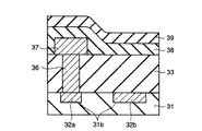
【0003】
まず、図21に示すように、リソグラフィ及びRIE(Reactive Ion Etching)によりシリコン酸化膜31がパターニングされ、シリコン酸化膜31内に溝31bが形成される。次に、全面に金属配線材が形成され、この金属配線材により溝31bが埋め込まれる。その後、CMP(Chemical Mechanical Polish)により、シリコン酸化膜31の表面が露出されるまで、金属配線材が平坦化され、シリコン酸化膜31内に第1の金属配線32a及び回路置換のためのフューズ配線32bが形成される。
【0004】
次に、全面にTEOS(Tetra Ethyl Ortho Silicate)膜33が形成される。このTEOS膜33が選択的に除去され、第1の金属配線32a上に接続孔36が形成される。次に、全面に金属材が形成され、この金属材により接続孔36が埋め込まれる。その後、CMPにより、TEOS膜33の表面が露出されるまで、金属材が平坦化される。次に、全面に金属配線材が形成され、この金属配線材がパターニングされ、接続孔36上に接続孔36を介して第1の金属配線32aと接続する第2の金属配線37が形成される。
【0005】
次に、全面にTEOS膜(シリコン酸化膜)38が形成され、このTEOS膜38上にシリコン窒化膜39が形成される。このTEOS膜38及びシリコン窒化膜39は、パシベーション膜となる。
【0006】
次に、図22に示すように、シリコン窒化膜39上に感光性のポリイミド樹脂膜40が形成され、このポリイミド樹脂膜40がリソグラフィによりパターニングされる。これにより、第2の金属配線37上及びフューズ配線32b上のシリコン窒化膜39の表面が露出される。
【0007】
次に、図23に示すように、第1の条件のRIEによりシリコン窒化膜39が除去される。さらに、第1の条件から第2の条件へ連続して変化させ、この第2の条件のRIEにより、第2の金属配線37上のTEOS膜38が除去されるとともに、フューズ配線32b上のTEOS膜38、33が除去される。この際、フューズ配線32b上には、フューズ配線32bの溶断時に配線材料が飛び散ることを防止するために薄いTEOS膜33aが残される。
【0008】
以上のようにして、第2の金属配線37上にパッド開孔41が形成され、フューズ配線32b上にフューズ窓42が形成される。
【0009】
【発明が解決しようとする課題】
上記従来技術によるフューズ窓42の形成において、図23に示すA部のようにTEOS膜33aを薄く残存させるためには、まず除去すべきTEOS膜33の膜厚を予め算出し、この膜厚とエッチング速度からエッチング時間を算出し、このエッチング時間によりエッチングは制御されていた。
【0010】
しかしながら、実際、TEOS膜33の膜厚にはばらつきがあり、かつエッチングの均一性にもばらつきがある。このため、エッチング時間を制御することによってフューズ配線12b上に適切な膜厚のTEOS膜を残存させることが非常に困難であった。
【0011】
つまり、例えばTEOS膜の膜厚が厚い状態で残存した場合、フューズ配線の溶断が難しくなり、一方、例えばTEOS膜が全て除去されてしまった場合、フューズ配線の溶断時に配線材料の飛び散りが生じ、近辺の配線がショートするという問題が生じていた。
【0012】
本発明は上記課題を解決するためになされたものであり、その目的とするところは、絶縁膜を制御性よく加工することが可能な半導体装置及びその製造方法を提供することにある。
【0013】
【課題を解決するための手段】
本発明は、前記目的を達成するために以下に示す手段を用いている。
【0014】
本発明の半導体装置の製造方法は、第1の絶縁膜内に第1の金属配線と配線を選択的に形成する工程と、全面に第2の絶縁膜を形成する工程と、前記第2の絶縁膜上にSOG膜を形成する工程と、前記SOG膜上に第3の絶縁膜を形成する工程と、前記第1の金属配線上の前記第2、第3の絶縁膜及び前記SOG膜内に接続孔を形成する工程と、前記接続孔上に前記第1の金属配線と接続する第2の金属配線を選択的に形成する工程と、全面に第4の絶縁膜を形成する工程と、前記第4の絶縁膜上に第5の絶縁膜を形成する工程と、前記第2の配線の上方及び前記配線の上方の前記第5の絶縁膜の表面を露出するように、前記第5の絶縁膜上に樹脂膜を形成する工程と、第1の条件を用いたドライエッチングにより、前記第5の絶縁膜を除去する工程と、第2の条件を用いたドライエッチングにより、前記第2の金属配線上の前記第4の絶縁膜を除去して前記第2の金属配線の表面を露出するパッド開口を形成するとともに、前記配線上の前記第3、第4の絶縁膜を除去して前記SOG膜の表面を露出する第1の開口部を形成する工程と、エッチングにより、前記配線上の前記SOG膜を除去し、前記第2の絶縁膜の表面を露出する第2の開口部を形成する工程とを含んでいる。
【0015】
上記本発明の半導体装置の製造方法において、前記SOG膜は無機SOG膜であり、前記第2、第3の絶縁膜はシリコン酸化膜、シリコン窒化膜、又は有機シリコン酸化膜のいずれかからなる膜であればよい。
【0016】
上記本発明の半導体装置の製造方法において、前記SOG膜を除去する工程における前記エッチングは、等方性エッチングであることが望ましい。また、前記SOG膜を除去する工程における前記エッチングは、CF4を含むガスあるいはCF4単ガスを用いたアッシャー処理、CF4を含むガスあるいはCF4単ガスを用いたCDE処理、あるいはアルカリ溶剤を用いたウエットエッチング処理のいずれかにより行われるとよい。
【0017】
上記本発明の半導体装置の製造方法において、前記ドライエッチングはRIE法であり、前記第2の条件はエッチングレートが前記第3、第4の絶縁膜>前記SOG膜、かつ前記第3、第4の絶縁膜>前記第2の金属配線の関係となる条件であることが望ましい。
【0018】
上記本発明の半導体装置の製造方法において、前記第1の絶縁膜内に形成される前記配線は、フューズ配線であることが望ましい。
【0019】
本発明の半導体装置は、第1の絶縁膜内に形成された配線と、前記第1の絶縁膜及び前記配線上に形成された第2の絶縁膜と、前記第2の絶縁膜上に形成されたSOG膜と、前記SOG膜上に形成された第3の絶縁膜と、前記配線上の前記第3の絶縁膜及び前記SOG膜内に形成された開口部とを具備している。
【0020】
本発明の他の半導体装置は、第1の絶縁膜内に形成された配線と、前記配線上に形成された第2の絶縁膜と、前記第2の絶縁膜上に形成されたSOG膜と、前記SOG膜上に形成された第3の絶縁膜と、前記配線上の前記第3の絶縁膜内に形成された第1の開口部と、前記第1の開口部と連通し、前記SOG膜内に形成された第2の開口部とを具備している。
【0021】
上記本発明の半導体装置において、前記第2の開口部の上面の開口は前記第1の開口部の開口よりも大きく、前記第2の開口部の底面の開口は前記第2の開口部の上面の開口よりも小さく、前記第2の開口部の側面は曲面を有している。
【0022】
上記本発明の半導体装置において、前記SOG膜は無機SOG膜であり、前記第2、第3の絶縁膜はシリコン酸化膜、シリコン窒化膜、又は有機シリコン酸化膜のいずれかからなる膜であればよい。また、前記配線は、フューズ配線であることが望ましい。
【0023】
上記本発明の半導体装置において、前記第2の絶縁膜内に形成された前記配線と前記第2の開口部とを接続する接続孔とをさらに具備し、前記第1、第2の開口部及び前記接続孔は金属材で埋め込まれていてもよい。
【0024】
また、本発明の他の半導体装置は、第1の絶縁膜上に形成された第2の絶縁膜と、前記第2の絶縁膜上に形成された第3の絶縁膜と、前記第3の絶縁膜上に形成された第4の絶縁膜と、前記第1の絶縁膜内に形成された第1の配線と、前記第3の絶縁膜内に形成された第2の配線と、前記第2の絶縁膜内に形成された前記第1の配線と前記第2の配線とを接続する第1の接続孔と、前記第4の絶縁膜内に形成された前記第2の配線と接続する第2の接続孔と、前記第2の配線の上面の開口は前記第2の接続孔の開口よりも大きく、前記第2の配線の底面の開口は前記第2の配線の上面の開口よりも小さく、前記第2の配線の側面は曲面を有している。
【0025】
【発明の実施の形態】
本発明の実施の形態を以下に図面を参照して説明する。
【0026】
[第1の実施形態]
本発明の第1の実施形態は、フューズ配線上の層間膜が、カバー膜として残すべき層間膜と、エッチングで除去すべき層間膜とから形成され、このように層間膜が積層化されることにより、フューズ配線上の層間膜の膜厚を制御している。以下、本発明の第1の実施形態に係わる半導体装置の製造方法について説明する。
【0027】
まず、図1に示すように、リソグラフィ及びRIE(Reactive Ion Etching)によりシリコン酸化膜11がパターニングされ、シリコン酸化膜11内に溝11aが形成される。次に、全面に金属配線材が形成され、この金属配線材により溝11aが埋め込まれる。その後、CMP(Chemical Mechanical Polish)により、シリコン酸化膜11の表面が露出されるまで、金属配線材が平坦化され、シリコン酸化膜11内に第1の金属配線12a及び回路置換のためのフューズ配線12bが形成される。
【0028】
次に、図2に示すように、全面に例えば50nm乃至150nmの膜厚を有するシリコン酸化膜13が形成され、このシリコン酸化膜13上に所定の膜厚を有する無機SOG(Spin On Glass)膜14が塗布される。このシリコン酸化膜13は、レーザによりフューズ配線12bを加工(溶断又は溶接)して回路置換を行う際、フューズ配線12bの材料が飛び散ることを防止するカバー膜である。従って、シリコン酸化膜13の膜厚は、カバー膜としての役割を十分果たすことが可能な膜厚で形成される。また、SOG膜14はシリコン酸化させるために200℃乃至400℃程度の温度で焼き固められ、この際のSOG膜14の膜厚は40nm以上とする。
【0029】
次に、図3に示すように、SOG膜14上に層間膜であるシリコン酸化膜15が形成される。次に、シリコン酸化膜13、15及びSOG膜14が除去され、第1の金属配線12a上に接続孔16が形成される。次に、全面に金属材が形成され、この金属材により接続孔16が埋め込まれる。その後、CMPにより、シリコン酸化膜15の表面が露出されるまで、金属材が平坦化される。次に、全面に金属配線材が形成され、この金属配線材がパターニングされる。その結果、接続孔16上に、接続孔16を介して第1の金属配線12aと接続する第2の金属配線17が形成される。
【0030】
次に、図4に示すように、全面にTEOS(Tetra Ethyl Ortho Silicate)膜(シリコン酸化膜)18が形成され、このTEOS膜18上にシリコン窒化膜19が形成される。このTEOS膜18及びシリコン窒化膜19は、パシベーション膜となる。
【0031】
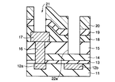
次に、図5に示すように、シリコン窒化膜19上に感光性のポリイミド樹脂膜20が形成され、このポリイミド樹脂膜20がリソグラフィによりパターニングされる。これにより、第2の金属配線17上及びフューズ配線12b上のシリコン窒化膜19の表面が露出される。
【0032】
次に、図6に示すように、第1の条件を用いたドライエッチングにより、シリコン窒化膜19が除去される。さらに、第1の条件から第2の条件へ連続して変化させ、この第2の条件を用いたドライエッチングにより、第2の金属配線17上のTEOS膜18が除去されるとともに、SOG膜14をストッパーとしてフューズ配線12b上のTEOS膜18及びシリコン酸化膜15が除去される。その結果、第2の金属配線17の表面を露出するパッド開口21が形成されるとともに、フューズ配線12b上にSOG膜14の表面を露出する第1の開口部22aが形成される。
【0033】
ここで、ドライエッチングとしては、例えばRIE法が用いられる。また、第1の条件は、例えばCHF3/CF4/O2ガス系で、TEOS膜18とシリコン窒化膜19がほぼ同じエッチング速度の関係となるような条件である。また、第2の条件は、例えばC4F8/CO/Arガス系で、エッチングレートがシリコン酸化膜15及びTEOS膜18>SOG膜14、かつシリコン酸化膜15及びTEOS膜18>第2の金属配線17の関係となるような条件である。このとき、第2の条件において、シリコン酸化膜15及びTEOS膜18の対SOG膜14の選択比は20乃至30程度とることができ、シリコン酸化膜15及びTEOS膜18の対第2の金属配線17の選択比は100程度とることができる。このように選択比が高いことより、例えばシリコン酸化膜15の膜厚が非常に厚い場合でも、第2の金属配線17の表面が除去されることなく、シリコン酸化膜15のみを確実に除去できる。
【0034】
尚、第2の条件によってエッチングする際、SOG膜14表面に10nm以下の膜厚を有するSOG改質膜(図示せず)が形成される。このため、ArスパッタによりSOG改質膜を除去する。但し、このArスパッタ工程は省略することも可能である。
【0035】
次に、図7に示すように、等方性エッチングにより、シリコン酸化膜13の表面が露出するまで、SOG膜14が等方的に除去される。その結果、第1の開口部22aと連通し、シリコン酸化膜13の表面を露出する第2の開口部22bが形成される。つまり、フューズ配線12b上には、カバー膜となるシリコン酸化膜13が残された状態となる。
【0036】
ここで、等方性エッチングは、CF4を含むガスあるいはCF4単ガスを用いたアッシャー処理又はCDE(Chemical Dry Etching)処理、若しくはアルカリ溶剤を用いたウエットエッチング処理により行われる。アッシャー処理又はCDE(Chemical Dry Etching)処理では、CF4プラズマを発生させ、このプラズマから生じたフッ素ラジカルによりエッチングが行われる。このような方法で等方性エッチングが行われた場合、SOG膜14の対シリコン酸化膜13の選択比は50以上とることができる。
【0037】
その後、最上層配線のパッド表面に付着したエッチングによる堆積物がコリン液及び水洗処理により除去される。以上のようにして、第2の金属配線17上にはパッド開口21が形成され、フューズ配線12b上には第1、第2の開口部22a、22bからなるフューズ窓22が形成される。
【0038】
尚、フューズ窓22の第2の開口部22bは、SOG膜14が等方的に除去されて形成されている。このため、第2の開口部22bの上面の開口は、第1の開口部22aの開口よりも大きく、第2の開口部22bの底面の開口は、前記第2の開口部22bの上面の開口よりも小さくなっている。また、第2の開口部22bの側面は曲面を有しており、つまり第2の開口部22bの底面の角が丸みを帯びた形状となっている。
【0039】
また、上述したエッチングにおいて、無機SOG膜は膜中にOH基を含み親水性であるため、OH基を持つアルカリ溶液が膜中に浸透されてエッチングが行われる。これに対し、シリコン酸化膜は撥水性であるため、アルカリ溶液が浸透せず、エッチングが行われない。また、CDEあるいはアッシャーを用いたCF4を含むガスあるいはCF4の単ガスでは、無機SOG膜のHが、CF4のFラジカルと反応するため、エッチングが行われる。これに対し、シリコン酸化膜はエッチングにイオンアシストが必要であるため、ラジカル成分だけではエッチングされにくい。さらに、膜構造においては、シリコン酸化膜はCVDで形成されるため緻密な膜であるのに対し、無機SOG膜は塗布型の装置で成膜してポーラスな膜を形成するため膜の結合が弱い。これらの原因から、シリコン酸化膜と無機シリコン酸化膜は上述する方法により高選択エッチングが可能である。
【0040】
上記本発明の第1の実施形態によれば、フューズ配線12b上の層間膜は、カバー膜として残すべきシリコン酸化膜13と、エッチングで除去すべきSOG膜14及びシリコン酸化膜15とから形成され、層間膜が積層化されている。従って、フューズ配線12b上の層間膜を加工する際、シリコン酸化膜13の表面でエッチングを停止することにより、従来よりも制御性よくフューズ配線12b上の層間膜を加工できる。
【0041】
さらに、層間膜の一部が低誘電率膜であるSOG膜14で形成されているため、配線間の容量の低減化が図られる。
【0042】
尚、層間膜は、SOG膜14とシリコン酸化膜15からなる多層構造に限定されず、例えばSOG膜のみからなる単層構造でもよい。この場合、上記実施の形態の効果と同様の効果が得られるだけでなく、さらに配線間の容量を低減できる。
【0043】
また、シリコン酸化膜13、15は、例えば、TEOS膜、シリコン窒化膜、有機シリコン酸化膜に変えてもよい。
【0044】
また、フューズ窓22の形成の際、第2の金属配線17の表面に多少のダメージは生じるが、第2の金属配線17は導通可能であれば十分であるため、素子の性能には問題ない。
【0045】
[第2の実施形態]
本発明の第2の実施形態は、第1の実施形態で示すようなフーズ配線の形成法を、例えば、深さ制御が必要な配線の絶縁膜の加工に利用した例である。以下、本発明の第2の実施形態に係わる半導体装置の製造方法について説明する。
【0046】
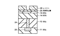
まず、図8に示すように、シリコン酸化膜11内に配線23が形成された後、全面にシリコン酸化膜13が形成される。このシリコン酸化膜13内に金属材で埋め込まれた接続孔24が形成される。次に、全面に後述する配線の深さの膜厚を有する無機SOG(Spin On Glass)膜14が塗布される。このSOG膜14上にシリコン酸化膜15が形成され、このシリコン酸化膜15上に反射防止膜25が形成される。この反射防止膜25上にレジスト膜26が形成されてパターニングされる。
【0047】
次に、図9に示すように、パターニングされたレジスト膜26をマスクとして、CHF3/CF4/O2ガス系を用いたRIEにより、反射防止膜25が除去される。さらに、連続してガスを変化させ、第1の実施形態と同様に、対SOG膜14と高選択比となる条件で、C4F8/CO/Arガス系を用いたRIEにより、SOG膜14をストッパーとしてシリコン酸化膜15が除去される。
【0048】
次に、図10に示すように、O2ガスを用いたアッシャー処理により、レジスト膜26と反射防止膜25が剥離除去される。
【0049】
尚、シリコン酸化膜15をエッチングする際、SOG膜14表面に10nm以下の膜厚を有するSOG改質膜(図示せず)が形成される。このため、レジスト膜26と反射防止膜25が剥離除去後、ArスパッタによりSOG改質膜を除去する。但し、このArスパッタ工程は省略することも可能である。
【0050】
次に、図11に示すように、等方性エッチングにより、シリコン酸化膜13及び接続孔24の表面が露出するまで、SOG膜14が等方的に除去される。その結果、配線溝27が形成される。ここで、等方性エッチングは、CF4を含むガスあるいはCF4単ガスを用いたアッシャー処理又はCDE(Chemical Dry Etching)処理、若しくはアルカリ溶剤を用いたウエットエッチング処理により行われる。
【0051】
次に、図12に示すように、CMP処理等により、シリコン酸化膜15が除去される。
【0052】
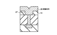
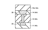
次に、図13に示すように、全面に配線材料28が形成され、配線溝27が埋め込まれる。ここで、配線材料28としては、Al、Al−Cu、Al−Si−Cu、W、WSi、Cu、Ag等の金属材料を用いればよい。その後、図14に示すように、CMP処理等により、SOG膜14の表面が露出するまで配線材料28が平坦化され、配線29が形成される。
【0053】
次に、図15に示すように、全面にシリコン酸化膜15aが形成される。その後、図16に示すように、シリコン酸化膜15a上に反射防止膜25aが形成され、この反射防止膜25a上にレジスト膜26aが形成されてパターニングされる。
【0054】
次に、図17に示すように、パターニングされたレジスト膜26aをマスクとして、CHF3/CF4/O2ガス系を用いたRIEにより、反射防止膜25が除去される。さらに、連続してガスを変化させ、第1の実施形態と同様に、対SOG膜14及び配線29と高選択比となる条件で、C4F8/CO/Arガス系を用いたRIEにより、SOG膜14をストッパーとしてシリコン酸化膜15aが除去される。その後、図18に示すように、O2ガスを用いたアッシャー処理により、レジスト膜26aと反射防止膜25aが剥離除去される。その結果、シリコン酸化膜15a内に、配線29と接続する接続孔30が形成される。
【0055】
次に、図19に示すように、全面に配線材料28aが形成され、接続孔30が埋め込まれる。その後、図20に示すように、CMP処理等により、シリコン酸化膜15aの表面が露出するまで配線材料28aが平坦化される。このようにして、多層配線構造の半導体装置が形成される。
【0056】
上記本発明の第2の実施形態によれば、配線29は、配線の上部が下部よりも大きな面積を有し、角に丸みを帯びた形状とすることができる。これにより、通常配線の角で発生する電界集中を抑制できる。
【0057】
さらに、層間膜の一部が低誘電率膜であるSOG膜14で形成されているため、配線間の容量の低減化が図られる。これは、微細加工技術に大きなメリットとなる。
【0058】
尚、配線29の上部、下部に形成される絶縁膜は、シリコン酸化膜13、15、30に限定されない。例えば、シリコン窒化膜、シリコン酸化窒化膜、有機シリコン酸化膜、SiC膜等の層間絶縁膜を用いることが可能である。
【0059】
また、配線溝27を配線材料28で埋め込む際、上部のシリコン酸化膜15は取り除かず、電解メッキにより配線材料28を成長させて配線溝27を埋め込み、CMP処理により配線29を形成してもよい。
【0060】
また、配線溝27を配線材料28で埋め込む前に、TiN、Ti、Nb等のバリアメタルを形成してもよいし、バリアとなる絶縁膜を形成してもよい。
【0061】
その他、本発明は、その要旨を逸脱しない範囲で、種々変形して実施することが可能である。
【0062】
【発明の効果】
以上説明したように本発明によれば、絶縁膜を制御性よく加工することが可能な半導体装置及びその製造方法を提供できる。
【図面の簡単な説明】
【図1】本発明の第1の実施形態に係わる半導体装置の製造工程を示す断面図。
【図2】図1に続く、本発明の第1の実施形態に係わる半導体装置の製造工程を示す断面図。
【図3】図2に続く、本発明の第1の実施形態に係わる半導体装置の製造工程を示す断面図。
【図4】図3に続く、本発明の第1の実施形態に係わる半導体装置の製造工程を示す断面図。
【図5】図4に続く、本発明の第1の実施形態に係わる半導体装置の製造工程を示す断面図。
【図6】図5に続く、本発明の第1の実施形態に係わる半導体装置の製造工程を示す断面図。
【図7】図6に続く、本発明の第1の実施形態に係わる半導体装置の製造工程を示す断面図。
【図8】本発明の第2の実施形態に係わる半導体装置の製造工程を示す断面図。
【図9】図8に続く、本発明の第2の実施形態に係わる半導体装置の製造工程を示す断面図。
【図10】図9に続く、本発明の第2の実施形態に係わる半導体装置の製造工程を示す断面図。
【図11】図10に続く、本発明の第2の実施形態に係わる半導体装置の製造工程を示す断面図。
【図12】図11に続く、本発明の第2の実施形態に係わる半導体装置の製造工程を示す断面図。
【図13】図12に続く、本発明の第2の実施形態に係わる半導体装置の製造工程を示す断面図。
【図14】図13に続く、本発明の第2の実施形態に係わる半導体装置の製造工程を示す断面図。
【図15】図14に続く、本発明の第2の実施形態に係わる半導体装置の製造工程を示す断面図。
【図16】図15に続く、本発明の第2の実施形態に係わる半導体装置の製造工程を示す断面図。
【図17】図16に続く、本発明の第2の実施形態に係わる半導体装置の製造工程を示す断面図。
【図18】図17に続く、本発明の第2の実施形態に係わる半導体装置の製造工程を示す断面図。
【図19】図18に続く、本発明の第2の実施形態に係わる半導体装置の製造工程を示す断面図。
【図20】図19に続く、本発明の第2の実施形態に係わる半導体装置の製造工程を示す断面図。
【図21】従来技術による半導体装置の製造工程を示す断面図。
【図22】図21に続く、従来技術による半導体装置の製造工程を示す断面図。
【図23】図22に続く、従来技術による半導体装置の製造工程を示す断面図。
【符号の説明】
11、13、15、15a…シリコン酸化膜、
11a…溝、
12a…第1の金属配線、
12b…フューズ配線、
14…SOG膜、
16、24、30…接続孔、
17…第2の金属配線、
18…TEOS膜(シリコン酸化膜)、
19…シリコン窒化膜、
20…ポリイミド樹脂膜、
21…パッド開口、
22…フューズ窓、
22a…第1の開口部、
22b…第2の開口部、
23、29…配線、
25、25a…反射防止膜、
26、26a…レジスト膜、
27…配線溝、
28、28a…配線材料。[0001]
BACKGROUND OF THE INVENTION
The present invention relates to a semiconductor device having a fuse wiring for circuit replacement and a method for manufacturing the same.
[0002]
[Prior art]
2. Description of the Related Art Conventionally, in a DRAM (Dynamic Random Access Memory) or the like, for example, a device having a repair circuit for replacing a defective cell with a spare cell is known for improving the product yield. Here, for circuit replacement from a defective cell to a spare cell, for example, a fuse wiring of a type in which wiring of aluminum or the like is burned out by a laser has been used. Such a fuse wiring is formed as follows.
[0003]
First, as shown in FIG. 21, the
[0004]
Next, a TEOS (Tetra Ethyl Ortho Silicate)
[0005]
Next, a TEOS film (silicon oxide film) 38 is formed on the entire surface, and a
[0006]
Next, as shown in FIG. 22, a photosensitive
[0007]
Next, as shown in FIG. 23, the
[0008]
As described above, the pad opening 41 is formed on the
[0009]
[Problems to be solved by the invention]
In forming the
[0010]
Actually, however, the thickness of the TEOS
[0011]
That is, for example, when the TEOS film remains in a thick state, it becomes difficult to blow the fuse wiring. On the other hand, for example, when the TEOS film is completely removed, the wiring material is scattered when the fuse wiring is blown, There was a problem that a nearby wiring was short-circuited.
[0012]
The present invention has been made to solve the above-described problems, and an object of the present invention is to provide a semiconductor device capable of processing an insulating film with good controllability and a method for manufacturing the same.
[0013]
[Means for Solving the Problems]
In order to achieve the above object, the present invention uses the following means.
[0014]
The method of manufacturing a semiconductor device according to the present invention includes a step of selectively forming a first metal wiring and a wiring in a first insulating film, a step of forming a second insulating film over the entire surface, A step of forming an SOG film on the insulating film; a step of forming a third insulating film on the SOG film; and the second and third insulating films on the first metal wiring and in the SOG film Forming a connection hole on the connection hole; selectively forming a second metal wiring connected to the first metal wiring on the connection hole; forming a fourth insulating film on the entire surface; Forming a fifth insulating film on the fourth insulating film; and exposing the surface of the fifth insulating film above the second wiring and above the wiring. The step of forming a resin film on the insulating film and the fifth insulating film are removed by dry etching using the first condition. And removing the fourth insulating film on the second metal wiring to form a pad opening exposing the surface of the second metal wiring by dry etching using the second condition. Removing the third and fourth insulating films on the wiring to form a first opening exposing the surface of the SOG film, and removing the SOG film on the wiring by etching. And a step of forming a second opening exposing the surface of the second insulating film.
[0015]
In the method of manufacturing a semiconductor device of the present invention, the SOG film is an inorganic SOG film, and the second and third insulating films are a film made of any one of a silicon oxide film, a silicon nitride film, and an organic silicon oxide film. If it is.
[0016]
In the method for manufacturing a semiconductor device according to the present invention, the etching in the step of removing the SOG film is preferably isotropic etching. Further, the etching in the step of removing the SOG film, ashing using a gas or CF 4 single gas containing CF 4, CDE process using a gas or CF 4 single gas containing CF 4, or the alkali solvent It may be performed by any of the wet etching processes used.
[0017]
In the method of manufacturing a semiconductor device of the present invention, the dry etching is an RIE method, and the second condition is that the etching rate is the third and fourth insulating films> the SOG film, and the third and fourth It is desirable that the conditions satisfy the relationship of insulating film> second metal wiring.
[0018]
In the semiconductor device manufacturing method of the present invention, it is preferable that the wiring formed in the first insulating film is a fuse wiring.
[0019]
A semiconductor device according to the present invention is formed on a wiring formed in a first insulating film, a second insulating film formed on the first insulating film and the wiring, and a second insulating film. And a third insulating film formed on the SOG film, and an opening formed in the third insulating film and the SOG film on the wiring.
[0020]
Another semiconductor device of the present invention includes a wiring formed in the first insulating film, a second insulating film formed on the wiring, an SOG film formed on the second insulating film, A third insulating film formed on the SOG film; a first opening formed in the third insulating film on the wiring; and the first opening. And a second opening formed in the film.
[0021]
In the semiconductor device of the present invention, the opening on the upper surface of the second opening is larger than the opening on the first opening, and the opening on the bottom of the second opening is on the upper surface of the second opening. The side surface of the second opening has a curved surface.
[0022]
In the semiconductor device according to the present invention, the SOG film is an inorganic SOG film, and the second and third insulating films are films made of any one of a silicon oxide film, a silicon nitride film, and an organic silicon oxide film. Good. The wiring is preferably a fuse wiring.
[0023]
The semiconductor device according to the present invention further includes a connection hole connecting the wiring formed in the second insulating film and the second opening, and the first and second openings, The connection hole may be embedded with a metal material.
[0024]
Another semiconductor device of the present invention includes a second insulating film formed on the first insulating film, a third insulating film formed on the second insulating film, and the third insulating film. A fourth insulating film formed on the insulating film; a first wiring formed in the first insulating film; a second wiring formed in the third insulating film; A first connection hole connecting the first wiring and the second wiring formed in the second insulating film and a second wiring formed in the fourth insulating film; The opening of the upper surface of the second connection hole and the second wiring is larger than the opening of the second connection hole, and the opening of the bottom surface of the second wiring is larger than the opening of the upper surface of the second wiring. The side surface of the second wiring is small and has a curved surface.
[0025]
DETAILED DESCRIPTION OF THE INVENTION
Embodiments of the present invention will be described below with reference to the drawings.
[0026]
[First Embodiment]
In the first embodiment of the present invention, an interlayer film on a fuse wiring is formed of an interlayer film to be left as a cover film and an interlayer film to be removed by etching, and the interlayer films are laminated in this way. Thus, the film thickness of the interlayer film on the fuse wiring is controlled. The semiconductor device manufacturing method according to the first embodiment of the present invention will be described below.
[0027]
First, as shown in FIG. 1, the
[0028]
Next, as shown in FIG. 2, a
[0029]
Next, as shown in FIG. 3, a
[0030]
Next, as shown in FIG. 4, a TEOS (Tetra Ethyl Ortho Silicate) film (silicon oxide film) 18 is formed on the entire surface, and a
[0031]
Next, as shown in FIG. 5, a photosensitive
[0032]
Next, as shown in FIG. 6, the
[0033]
Here, as the dry etching, for example, the RIE method is used. The first condition is, for example, a CHF 3 / CF 4 / O 2 gas system, such that the
[0034]
When etching is performed under the second condition, an SOG modified film (not shown) having a thickness of 10 nm or less is formed on the surface of the
[0035]
Next, as shown in FIG. 7, the
[0036]
Here, isotropic etching, ashing or CDE (Chemical Dry Etching) process using a gas or CF 4 single gas containing CF 4, or carried out by a wet etching process using an alkali solution. In the asher processing or CDE (Chemical Dry Etching) processing, CF 4 plasma is generated and etching is performed by fluorine radicals generated from the plasma. When isotropic etching is performed by such a method, the selection ratio of the
[0037]
Thereafter, the deposit by etching adhering to the pad surface of the uppermost layer wiring is removed by a choline solution and a water washing treatment. As described above, the
[0038]
The
[0039]
In the etching described above, the inorganic SOG film contains OH groups in the film and is hydrophilic, so that an alkaline solution having OH groups is permeated into the film to perform etching. On the other hand, since the silicon oxide film is water repellent, the alkaline solution does not penetrate and etching is not performed. Further, in the single-gas in the gas or CF 4 containing CF 4 with a CDE or Usher, H of the inorganic SOG film, to react with F radicals CF 4, etching is performed. On the other hand, since the silicon oxide film needs ion assist for etching, it is difficult to etch with only a radical component. Furthermore, in the film structure, the silicon oxide film is a dense film because it is formed by CVD, whereas the inorganic SOG film is formed by a coating type apparatus to form a porous film, so that the film is bonded. weak. For these reasons, the silicon oxide film and the inorganic silicon oxide film can be highly selectively etched by the method described above.
[0040]
According to the first embodiment of the present invention, the interlayer film on the
[0041]
Further, since a part of the interlayer film is formed of the
[0042]
The interlayer film is not limited to a multilayer structure composed of the
[0043]
Further, the
[0044]
Further, when the
[0045]
[Second Embodiment]
The second embodiment of the present invention is an example in which the method for forming a hood wiring as shown in the first embodiment is used for processing an insulating film of a wiring that requires depth control, for example. A method for manufacturing a semiconductor device according to the second embodiment of the present invention will be described below.
[0046]
First, as shown in FIG. 8, after the
[0047]
Next, as shown in FIG. 9, the antireflection film 25 is removed by RIE using a CHF 3 / CF 4 / O 2 gas system using the patterned resist
[0048]
Next, as shown in FIG. 10, the resist
[0049]
When the
[0050]
Next, as shown in FIG. 11, the
[0051]
Next, as shown in FIG. 12, the
[0052]
Next, as shown in FIG. 13, the wiring material 28 is formed on the entire surface, and the
[0053]
Next, as shown in FIG. 15, a
[0054]
Next, as shown in FIG. 17, the antireflection film 25 is removed by RIE using a CHF 3 / CF 4 / O 2 gas system using the patterned resist
[0055]
Next, as shown in FIG. 19, the
[0056]
According to the second embodiment of the present invention, the
[0057]
Further, since a part of the interlayer film is formed of the
[0058]
The insulating film formed on the upper and lower portions of the
[0059]
Further, when the
[0060]
Further, before the
[0061]
In addition, the present invention can be variously modified and implemented without departing from the scope of the invention.
[0062]
【The invention's effect】
As described above, according to the present invention, a semiconductor device capable of processing an insulating film with good controllability and a method for manufacturing the same can be provided.
[Brief description of the drawings]
FIG. 1 is a cross-sectional view showing a manufacturing process of a semiconductor device according to a first embodiment of the invention.
2 is a cross-sectional view showing the manufacturing process of the semiconductor device according to the first embodiment of the present invention, following FIG. 1;
3 is a cross-sectional view showing the manufacturing process of the semiconductor device according to the first embodiment of the present invention, following FIG. 2;
4 is a cross-sectional view showing the manufacturing process of the semiconductor device according to the first embodiment of the present invention, following FIG. 3;
5 is a cross-sectional view showing the manufacturing process of the semiconductor device according to the first embodiment of the present invention, following FIG. 4;
6 is a cross-sectional view showing the manufacturing process of the semiconductor device according to the first embodiment of the present invention, following FIG. 5;
7 is a cross-sectional view showing the manufacturing process of the semiconductor device according to the first embodiment of the present invention, following FIG. 6;
FIG. 8 is a cross-sectional view showing a manufacturing process of a semiconductor device according to the second embodiment of the present invention.
9 is a cross-sectional view showing the manufacturing process of the semiconductor device according to the second embodiment of the present invention, following FIG. 8;
FIG. 10 is a cross-sectional view showing the manufacturing process of the semiconductor device according to the second embodiment of the present invention, following FIG. 9;
FIG. 11 is a cross-sectional view showing the manufacturing process of the semiconductor device according to the second embodiment of the invention, following FIG. 10;
12 is a cross-sectional view showing the manufacturing process of the semiconductor device according to the second embodiment of the present invention, following FIG. 11;
13 is a cross-sectional view showing the manufacturing process of the semiconductor device according to the second embodiment of the present invention, following FIG. 12;
14 is a cross-sectional view showing the manufacturing process of the semiconductor device according to the second embodiment of the present invention, following FIG. 13;
15 is a cross-sectional view showing the manufacturing process of the semiconductor device according to the second embodiment of the present invention, following FIG. 14;
16 is a cross-sectional view showing the manufacturing process of the semiconductor device according to the second embodiment of the present invention, following FIG. 15;
FIG. 17 is a cross-sectional view showing the manufacturing process of the semiconductor device according to the second embodiment of the present invention, following FIG. 16;
18 is a cross-sectional view showing the manufacturing process of the semiconductor device according to the second embodiment of the present invention, following FIG. 17;
FIG. 19 is a cross-sectional view showing the manufacturing process of the semiconductor device according to the second embodiment of the present invention, following FIG. 18;
20 is a cross-sectional view showing the manufacturing process of the semiconductor device according to the second embodiment of the present invention, following FIG. 19;
FIG. 21 is a cross-sectional view showing a manufacturing process of a semiconductor device according to a conventional technique.
FIG. 22 is a cross-sectional view showing the manufacturing process of the semiconductor device according to the conventional technique, following FIG. 21;
FIG. 23 is a cross-sectional view showing the manufacturing process of the semiconductor device according to the conventional technique, following FIG. 22;
[Explanation of symbols]
11, 13, 15, 15a ... silicon oxide film,
11a ... groove,
12a ... 1st metal wiring,
12b ... fuse wiring,
14 ... SOG film,
16, 24, 30 ... connection holes,
17 ... second metal wiring,
18 ... TEOS film (silicon oxide film),
19 ... silicon nitride film,
20 ... polyimide resin film,
21 ... Pad opening,
22 ... fuse window,
22a ... first opening,
22b ... second opening,
23, 29 ... wiring,
25, 25a ... antireflection film,
26, 26a ... resist film,
27: Wiring groove,
28, 28a: wiring material.
Claims (13)
全面に第2の絶縁膜を形成する工程と、
前記第2の絶縁膜上にSOG膜を形成する工程と、
前記SOG膜上に第3の絶縁膜を形成する工程と、
前記第1の金属配線上の前記第2、第3の絶縁膜及び前記SOG膜内に接続孔を形成する工程と、
前記接続孔上に前記第1の金属配線と接続する第2の金属配線を選択的に形成する工程と、
全面に第4の絶縁膜を形成する工程と、
前記第4の絶縁膜上に第5の絶縁膜を形成する工程と、
前記第2の配線の上方及び前記配線の上方の前記第5の絶縁膜の表面を露出するように、前記第5の絶縁膜上に樹脂膜を形成する工程と、
第1の条件を用いたドライエッチングにより、前記第5の絶縁膜を除去する工程と、
第2の条件を用いたドライエッチングにより、前記第2の金属配線上の前記第4の絶縁膜を除去して前記第2の金属配線の表面を露出するパッド開口を形成するとともに、前記配線上の前記第3、第4の絶縁膜を除去して前記SOG膜の表面を露出する第1の開口部を形成する工程と、
エッチングにより、前記配線上の前記SOG膜を除去し、前記第2の絶縁膜の表面を露出する第2の開口部を形成する工程と
を含むことを特徴とする半導体装置の製造方法。A step of selectively forming a first metal wiring and a wiring in the first insulating film;
Forming a second insulating film on the entire surface;
Forming an SOG film on the second insulating film;
Forming a third insulating film on the SOG film;
Forming a connection hole in the second and third insulating films and the SOG film on the first metal wiring;
Selectively forming a second metal wiring connected to the first metal wiring on the connection hole;
Forming a fourth insulating film on the entire surface;
Forming a fifth insulating film on the fourth insulating film;
Forming a resin film on the fifth insulating film so as to expose the surface of the fifth insulating film above the second wiring and above the wiring;
Removing the fifth insulating film by dry etching using a first condition;
By dry etching using the second condition, the fourth insulating film on the second metal wiring is removed to form a pad opening exposing the surface of the second metal wiring, and on the wiring Removing the third insulating film and the fourth insulating film to form a first opening exposing the surface of the SOG film;
And a step of removing the SOG film on the wiring by etching to form a second opening exposing the surface of the second insulating film.
前記第1の絶縁膜及び前記配線上に形成された第2の絶縁膜と、
前記第2の絶縁膜上に形成されたSOG膜と、
前記SOG膜上に形成された第3の絶縁膜と、
前記配線上の前記第3の絶縁膜及び前記SOG膜内に形成された開口部と
を具備することを特徴とする半導体装置。A wiring formed in the first insulating film;
A second insulating film formed on the first insulating film and the wiring;
An SOG film formed on the second insulating film;
A third insulating film formed on the SOG film;
A semiconductor device comprising: the third insulating film on the wiring; and an opening formed in the SOG film.
前記配線上に形成された第2の絶縁膜と、
前記第2の絶縁膜上に形成されたSOG膜と、
前記SOG膜上に形成された第3の絶縁膜と、
前記配線上の前記第3の絶縁膜内に形成された第1の開口部と、
前記第1の開口部と連通し、前記SOG膜内に形成された第2の開口部と
を具備することを特徴とする半導体装置。A wiring formed in the first insulating film;
A second insulating film formed on the wiring;
An SOG film formed on the second insulating film;
A third insulating film formed on the SOG film;
A first opening formed in the third insulating film on the wiring;
A semiconductor device comprising: a second opening formed in the SOG film in communication with the first opening.
前記第1、第2の開口部及び前記接続孔は金属材で埋め込まれていることを特徴とする請求項8記載の半導体装置。A connection hole connecting the wiring formed in the second insulating film and the second opening;
9. The semiconductor device according to claim 8, wherein the first and second openings and the connection hole are embedded with a metal material.
前記第2の絶縁膜上に形成された第3の絶縁膜と、
前記第3の絶縁膜上に形成された第4の絶縁膜と、
前記第1の絶縁膜内に形成された第1の配線と、
前記第3の絶縁膜内に形成された第2の配線と、
前記第2の絶縁膜内に形成された前記第1の配線と前記第2の配線とを接続する第1の接続孔と、
前記第4の絶縁膜内に形成された前記第2の配線と接続する第2の接続孔と、前記第2の配線の上面の開口は前記第2の接続孔の開口よりも大きく、前記第2の配線の底面の開口は前記第2の配線の上面の開口よりも小さく、前記第2の配線の側面は曲面を有していることを特徴とする半導体装置。A second insulating film formed on the first insulating film;
A third insulating film formed on the second insulating film;
A fourth insulating film formed on the third insulating film;
A first wiring formed in the first insulating film;
A second wiring formed in the third insulating film;
A first connection hole connecting the first wiring and the second wiring formed in the second insulating film;
The second connection hole formed in the fourth insulating film and connected to the second wiring, and the opening of the upper surface of the second wiring is larger than the opening of the second connection hole. 2. The semiconductor device according to claim 2, wherein an opening on a bottom surface of the second wiring is smaller than an opening on an upper surface of the second wiring, and a side surface of the second wiring has a curved surface.
Priority Applications (1)
| Application Number | Priority Date | Filing Date | Title |
|---|---|---|---|
| JP2000087552A JP3670552B2 (en) | 2000-03-27 | 2000-03-27 | Semiconductor device and manufacturing method thereof |
Applications Claiming Priority (1)
| Application Number | Priority Date | Filing Date | Title |
|---|---|---|---|
| JP2000087552A JP3670552B2 (en) | 2000-03-27 | 2000-03-27 | Semiconductor device and manufacturing method thereof |
Publications (2)
| Publication Number | Publication Date |
|---|---|
| JP2001274247A JP2001274247A (en) | 2001-10-05 |
| JP3670552B2 true JP3670552B2 (en) | 2005-07-13 |
Family
ID=18603547
Family Applications (1)
| Application Number | Title | Priority Date | Filing Date |
|---|---|---|---|
| JP2000087552A Expired - Fee Related JP3670552B2 (en) | 2000-03-27 | 2000-03-27 | Semiconductor device and manufacturing method thereof |
Country Status (1)
| Country | Link |
|---|---|
| JP (1) | JP3670552B2 (en) |
Families Citing this family (6)
| Publication number | Priority date | Publication date | Assignee | Title |
|---|---|---|---|---|
| US7067896B2 (en) * | 2002-11-13 | 2006-06-27 | Taiwan Semiconductor Manufacturing Co., Ltd. | Microelectronic fabrication having edge passivated bond pad integrated with option selection device access aperture |
| JP2006049759A (en) * | 2004-08-09 | 2006-02-16 | Renesas Technology Corp | Semiconductor apparatus and manufacturing method thereof |
| JP2006073891A (en) * | 2004-09-03 | 2006-03-16 | Renesas Technology Corp | Semiconductor device and manufacturing method of semiconductor device |
| JP2007019188A (en) | 2005-07-06 | 2007-01-25 | Renesas Technology Corp | Semiconductor integrated circuit device and manufacturing method thereof |
| JP2007194475A (en) * | 2006-01-20 | 2007-08-02 | Elpida Memory Inc | Semiconductor device and manufacturing method thereof |
| JP4405488B2 (en) | 2006-08-30 | 2010-01-27 | 株式会社東芝 | Semiconductor device and manufacturing method of semiconductor device |
-
2000
- 2000-03-27 JP JP2000087552A patent/JP3670552B2/en not_active Expired - Fee Related
Also Published As
| Publication number | Publication date |
|---|---|
| JP2001274247A (en) | 2001-10-05 |
Similar Documents
| Publication | Publication Date | Title |
|---|---|---|
| US6861347B2 (en) | Method for forming metal wiring layer of semiconductor device | |
| US6171951B1 (en) | Dual damascene method comprising ion implanting to densify dielectric layer and forming a hard mask layer with a tapered opening | |
| US6846750B1 (en) | High precision pattern forming method of manufacturing a semiconductor device | |
| US5502007A (en) | Method of forming flat surface of insulator film of semiconductor device | |
| KR100267106B1 (en) | Method for fabricating multi-layer metal interconnection of semiconductor device | |
| US6815331B2 (en) | Method for forming metal wiring layer of semiconductor device | |
| KR20020042274A (en) | Method of forming interlayer connection and semiconductor devices formed by using the same | |
| JP3670552B2 (en) | Semiconductor device and manufacturing method thereof | |
| JP2004119950A (en) | Method for manufacturing semiconductor device | |
| US20070042600A1 (en) | Method for fabricating semiconductor device | |
| US6043165A (en) | Methods of forming electrically interconnected lines using ultraviolet radiation as an organic compound cleaning agent | |
| JP2004260001A (en) | Method for manufacturing semiconductor device | |
| KR100380348B1 (en) | A method for forming gate spacer of self-aligned contact | |
| JP3719672B2 (en) | Manufacturing method of semiconductor device | |
| US6664181B2 (en) | Method for fabricating semiconductor device | |
| JP3704030B2 (en) | Manufacturing method of semiconductor device | |
| US7326632B2 (en) | Method for fabricating metal wirings of semiconductor device | |
| KR100750821B1 (en) | Method for manufacturing a semiconductor device | |
| US20090263968A1 (en) | Method of fabricating semiconductor device | |
| KR100310172B1 (en) | Method for formimg metal layer of semiconductor devices | |
| KR20000050505A (en) | Method for forming contact hole of semiconductor device | |
| JP2001176963A (en) | Method for fabricating semiconductor device | |
| KR0179849B1 (en) | Wiring structure of semiconductor device and manufacturing method thereof | |
| KR100313537B1 (en) | Capacitor forming method | |
| JP2005101287A (en) | Semiconductor device manufacturing method and semiconductor device |
Legal Events
| Date | Code | Title | Description |
|---|---|---|---|
| A977 | Report on retrieval |
Free format text: JAPANESE INTERMEDIATE CODE: A971007 Effective date: 20040524 |
|
| TRDD | Decision of grant or rejection written | ||
| A01 | Written decision to grant a patent or to grant a registration (utility model) |
Free format text: JAPANESE INTERMEDIATE CODE: A01 Effective date: 20050412 |
|
| A61 | First payment of annual fees (during grant procedure) |
Free format text: JAPANESE INTERMEDIATE CODE: A61 Effective date: 20050414 |
|
| FPAY | Renewal fee payment (event date is renewal date of database) |
Free format text: PAYMENT UNTIL: 20080422 Year of fee payment: 3 |
|
| FPAY | Renewal fee payment (event date is renewal date of database) |
Free format text: PAYMENT UNTIL: 20090422 Year of fee payment: 4 |
|
| FPAY | Renewal fee payment (event date is renewal date of database) |
Free format text: PAYMENT UNTIL: 20100422 Year of fee payment: 5 |
|
| FPAY | Renewal fee payment (event date is renewal date of database) |
Free format text: PAYMENT UNTIL: 20100422 Year of fee payment: 5 |
|
| FPAY | Renewal fee payment (event date is renewal date of database) |
Free format text: PAYMENT UNTIL: 20110422 Year of fee payment: 6 |
|
| FPAY | Renewal fee payment (event date is renewal date of database) |
Free format text: PAYMENT UNTIL: 20130422 Year of fee payment: 8 |
|
| FPAY | Renewal fee payment (event date is renewal date of database) |
Free format text: PAYMENT UNTIL: 20140422 Year of fee payment: 9 |
|
| LAPS | Cancellation because of no payment of annual fees |