JP2004260001A - Method for manufacturing semiconductor device - Google Patents
Method for manufacturing semiconductor device Download PDFInfo
- Publication number
- JP2004260001A JP2004260001A JP2003049868A JP2003049868A JP2004260001A JP 2004260001 A JP2004260001 A JP 2004260001A JP 2003049868 A JP2003049868 A JP 2003049868A JP 2003049868 A JP2003049868 A JP 2003049868A JP 2004260001 A JP2004260001 A JP 2004260001A
- Authority
- JP
- Japan
- Prior art keywords
- film
- interlayer insulating
- insulating film
- wiring
- semiconductor device
- Prior art date
- Legal status (The legal status is an assumption and is not a legal conclusion. Google has not performed a legal analysis and makes no representation as to the accuracy of the status listed.)
- Granted
Links
Images


Classifications
-
- H—ELECTRICITY
- H01—ELECTRIC ELEMENTS
- H01L—SEMICONDUCTOR DEVICES NOT COVERED BY CLASS H10
- H01L21/00—Processes or apparatus adapted for the manufacture or treatment of semiconductor or solid state devices or of parts thereof
- H01L21/70—Manufacture or treatment of devices consisting of a plurality of solid state components formed in or on a common substrate or of parts thereof; Manufacture of integrated circuit devices or of parts thereof
- H01L21/71—Manufacture of specific parts of devices defined in group H01L21/70
- H01L21/768—Applying interconnections to be used for carrying current between separate components within a device comprising conductors and dielectrics
- H01L21/76801—Applying interconnections to be used for carrying current between separate components within a device comprising conductors and dielectrics characterised by the formation and the after-treatment of the dielectrics, e.g. smoothing
- H01L21/76802—Applying interconnections to be used for carrying current between separate components within a device comprising conductors and dielectrics characterised by the formation and the after-treatment of the dielectrics, e.g. smoothing by forming openings in dielectrics
- H01L21/76814—Applying interconnections to be used for carrying current between separate components within a device comprising conductors and dielectrics characterised by the formation and the after-treatment of the dielectrics, e.g. smoothing by forming openings in dielectrics post-treatment or after-treatment, e.g. cleaning or removal of oxides on underlying conductors
-
- H—ELECTRICITY
- H01—ELECTRIC ELEMENTS
- H01L—SEMICONDUCTOR DEVICES NOT COVERED BY CLASS H10
- H01L21/00—Processes or apparatus adapted for the manufacture or treatment of semiconductor or solid state devices or of parts thereof
- H01L21/70—Manufacture or treatment of devices consisting of a plurality of solid state components formed in or on a common substrate or of parts thereof; Manufacture of integrated circuit devices or of parts thereof
- H01L21/71—Manufacture of specific parts of devices defined in group H01L21/70
- H01L21/768—Applying interconnections to be used for carrying current between separate components within a device comprising conductors and dielectrics
- H01L21/76801—Applying interconnections to be used for carrying current between separate components within a device comprising conductors and dielectrics characterised by the formation and the after-treatment of the dielectrics, e.g. smoothing
- H01L21/76802—Applying interconnections to be used for carrying current between separate components within a device comprising conductors and dielectrics characterised by the formation and the after-treatment of the dielectrics, e.g. smoothing by forming openings in dielectrics
- H01L21/76807—Applying interconnections to be used for carrying current between separate components within a device comprising conductors and dielectrics characterised by the formation and the after-treatment of the dielectrics, e.g. smoothing by forming openings in dielectrics for dual damascene structures
- H01L21/76808—Applying interconnections to be used for carrying current between separate components within a device comprising conductors and dielectrics characterised by the formation and the after-treatment of the dielectrics, e.g. smoothing by forming openings in dielectrics for dual damascene structures involving intermediate temporary filling with material
Abstract
Description
【0001】
【発明の属する技術分野】
本発明は、配線層の形成に好適な半導体装置の製造方法に関する。
【0002】
【従来の技術】
半導体集積回路の大規模高集積化、高速化の要求に伴い、抵抗の低い多層配線材料、容量の小さい層間絶縁材料が必要になってきている。このため、以前は、多層配線材料としてアルミニウム(Al)合金が、層間絶縁膜材料としてシリコン(SiO)酸化物が用いられていたが、近時、前記の要求を満たすために、配線材料として銅(Cu)が用いられ、層間絶縁膜材料として低誘電体材料が用いられるようになっている。
【0003】
しかし、銅そのものの微細加工は非常に困難であるため、銅配線の形成には主にダマシン(Damascene)法が採用されている。ダマシン法は、絶縁膜に溝パターンやビアホールパターン等を形成した後、これらのパターン内へ銅材を埋め込み、次いで銅材を研磨(CMP:Chemical Mechanical Polishing)して配線を形成する方法である。ダマシン法には、溝とホールを同時に形成するデュアルダマシン(Dual Damascene)法と、これらを個別に形成するシングルダマシン(Single Damascene)法とがある。
【0004】
多くの半導体装置では、配線層が複数形成されており、その製造工程では、銅配線上にビアホールを形成する工程が必要とされる。しかし、銅は、それまで配線材料として使用されていたアルミニウム合金と比較すると、酸素プラズマに対する耐性が低い。このため、ビアホールの形成に使用したレジストマスクを除去する際に、アルミニウム合金の場合と同様のアッシング条件をそのまま用いると、コンタクト不良等の不具合が発生する可能性が高い。そこで、このような不具合を回避するために、アッシング時に銅配線の表面を露出させない加工方法が構築された。
【0005】
この加工方法では、銅配線と層間絶縁膜との間に拡散防止膜を形成しておき、層間絶縁膜への溝パターン又はビアホールパターンの形成を拡散防止膜で一旦停止する。そして、レジストマスクをアッシングにより除去し、その後に拡散防止膜をエッチングする。このような方法によれば、銅配線の表面がほとんど酸素プラズマに晒されないため、コンタクト不良等の不具合が防止される。
【0006】
しかし、拡散防止膜のエッチング時に銅配線の表面が少なくとも露出してしまう。このため、この時(銅配線の表面が露出した時)に、反応生成物が溝パターンの側壁部等に付着することが知られている。そこで、従来、最後のドライエッチングである拡散防止膜のエッチングを行った後に、薬液を使用したウェット処理を行い、反応生成物を除去している。
【0007】
【特許文献1】
特開平11−312669号公報
【特許文献2】
特開2001−284327号公報
【0008】
【発明が解決しようとする課題】
しかしながら、SiO2膜を層間絶縁膜として用いる場合には、上述の従来の方法で特に問題は生じていなかったが、近時、より低誘電率の層間絶縁膜としてSiOC膜を用いるようになると、コンタクト抵抗が上昇したり、歩留りが低下したり、信頼性が低下したりするようになった。
【0009】
本発明は、かかる問題点に鑑みてなされたものであって、SiOC膜を層間絶縁膜として用いた場合でも、コンタクト抵抗の上昇、歩留りの低下及び信頼性の低下を抑制することができる半導体装置の製造方法を提供することを目的とする。
【0010】
【課題を解決するための手段】
本願発明者は、前記課題を解決すべく、鋭意検討を重ねた結果、SiOC膜等のCを含有する絶縁膜を層間絶縁膜として用いると、反応生成物の生成量が、SiO2膜を用いた場合よりも多く、従来のようなウェット処理を行っただけでは、反応生成物を十分に除去することができないことを見出した。また、本願発明者は、残存した反応生成物が、既に形成されたビアホール内等に倒壊して後の銅配線の形成を妨害していることも見出した。そこで、ウェット処理によって、反応生成物を除去すべく、種々の薬液を用いて実験を行ったが、銅配線の表面及び低誘電体膜(層間絶縁膜)に悪影響を与えずに、完全に除去することはできなかった。
【0011】
そして、本願発明者が、更に鋭意検討を行った結果、以下に示す発明の諸態様に想到した。
【0012】
本発明に係る半導体装置の製造方法は、ダマシン法により配線を形成する工程を有する半導体装置の製造方法を対象とする。そして、この製造方法では、先ず、導電層上に、拡散防止膜及び層間絶縁膜を順次形成する。次に、前記層間絶縁膜に前記拡散防止膜まで到達する開口部を形成する。次いで、前記拡散防止膜の前記層間絶縁膜に形成された開口部から露出する部分を除去するドライエッチングを行う。その後、少なくとも前記開口部の内部に対して、酸素又は水素を含有するガスのプラズマを用いてプラズマ処理を行う。そして、前記開口部内に配線材料を埋め込む。
【0013】
本発明においては、ドライエッチングにより拡散防止膜の選択的な除去を行った後で、開口部内に配線材料を埋め込む前に、酸素又は水素を含有するガスのプラズマを用いたプラズマ処理を行う。このため、SiOC膜を層間絶縁膜として用い、ドライエッチングによって開口部の側壁に多量の反応生成物が付着した場合であっても、プラズマ処理によって反応生成物をほぼ完全に除去することが可能である。この結果、配線の形成の不良や信頼性の低下等の不具合を回避することができる。
【0014】
【発明の実施の形態】
以下、本発明の実施の形態に係る半導体装置の製造方法について添付の図面を参照して具体的に説明する。
【0015】
(第1の実施形態)
先ず、本発明の第1の実施形態について説明する。第1の実施形態は、本願発明を先ビア方式のデュアルダマシン法に適用したものである。図1乃至図6は、本発明の第1の実施形態に係る半導体装置の製造方法を工程順に示す断面図である。
【0016】
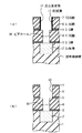
本実施形態では、先ず、Si基板等の半導体基板(図示せず)の表面にトランジスタ等の半導体素子(図示せず)を形成した後、半導体基板の上方に、図1(a)に示すように、層間絶縁膜1を形成する。次いで、この層間絶縁膜1に溝を形成し、その内部に、前記半導体素子に接続されるCu配線2を埋め込む。その後、層間絶縁膜1及びCu配線2上にSiC膜3、SiOC膜4(層間絶縁膜)、SiC膜5(エッチングストッパ膜)、SiOC膜6(第2の層間絶縁膜)、TEOS(Tetra Ethyl Ortho Silicate)膜7及びSiN膜8を順次形成する。SiC膜3、SiOC膜4、SiC膜5、SiOC膜6、TEOS膜7及びSiN膜8の各厚さは、夫々30nm乃至70nm、400nm乃至700nm、30nm乃至70nm、300nm乃至600nm、50nm乃至100nm、30nm乃至70nmである。SiC膜3は、Cu配線2中のCuの拡散を防止する拡散防止膜として機能する。また、SiN膜8は反射防止膜として機能する。
【0017】
続いて、図1(b)に示すように、ビアホール用の開口部が設けられたビアホール用のレジスト膜9をSiN膜8上に形成する。レジスト膜9の厚さは、例えば500nm乃至800nm程度である。
【0018】
次に、図2(a)に示すように、レジスト膜9をマスクとして用いながら、SiN膜8、TEOS膜7、SiOC膜6、SiC膜5及びSiOC膜4にビアホール10(開口部)を形成する。このときの各膜のエッチング条件は、次のとおりである。
【0019】
SiN膜8及びTEOS膜7のエッチングは、例えば、CF4の流量:100sccm、圧力:6.67Pa(50mTorr)、RF電源パワー:300W、時間:30秒間、温度:25℃の条件の下で連続して行う。
【0020】
SiOC膜6のエッチングは、例えば、CHF3の流量:10sccm、O2の流量:5sccm、Arの流量:750sccm、圧力:13.3Pa(100mTorr)、RF電源パワー:1000W、時間:45秒間、温度:25℃の条件の下で、SiC膜5をエッチングストッパとして用いて行う。
【0021】
SiC膜5及びSiOC膜4のエッチングは、先ず、例えば、CF4の流量:50sccm、CH2F2の流量:15sccm、O2の流量:5sccm、圧力:26.6Pa(200mTorr)、RF電源パワー:1000W、時間:30秒間、温度:25℃の条件の下で連続して行う。この条件では、SiC膜5とSiOC膜4との選択比が比較的小さい。次いで、SiOC膜4のエッチングが終了する前に、例えば、C4F6の流量:15sccm、O2の流量:30sccm、COの流量:500sccm、Arの流量:300sccm、圧力:5.33Pa(40mTorr)、RF電源パワー:1000W、時間:75秒間、温度:25℃の条件の下で、更にSiOC膜4のエッチングを行う。この条件では、SiOC膜4とSiC膜3との選択比が極めて大きく、SiC膜3はほとんどエッチングされない。
【0022】
ビアホール10を形成した後、図2(a)に示すように、レジスト膜9をアッシングにより除去する。このときのアッシング条件は、例えば、O2の流量:250sccm、圧力:10.7Pa(80mTorr)、RF電源パワー:150W、時間:120秒間、温度:25℃とする。
【0023】
次いで、図2(b)に示すように、ビアホール10内に埋め込むようにして全面に樹脂材11を形成する。樹脂材11の厚さは、例えばSiN膜8上で300nm乃至500nmとする。
【0024】
その後、図3(a)に示すように、樹脂材11の全面エッチングを行い、所定の高さの樹脂材11(埋め込み材)をビアホール内に残存させる。樹脂材11の高さは、SiOC膜4の厚さよりも小さい。なお、樹脂材の全面エッチングを行う代わりに、樹脂材11の現像を行うことによって、所定の高さの樹脂材11をビアホール内に残存させてもよい。
【0025】
続いて、図3(b)に示すように、配線溝用の開口部が設けられた配線溝用のレジスト膜12をSiN膜8上に形成する。レジスト膜12の厚さは、例えば500nm乃至800nm程度である。
【0026】
次に、図4(a)に示すように、レジスト膜12をマスクとして用いながら、SiN膜8、TEOS膜7及びSiOC膜6に配線溝13を形成する。このときの各膜のエッチング条件は、例えば、CF4の流量:100sccm、O2の流量:5sccm、圧力:13.3Pa(100mTorr)、RF電源パワー:1000W、時間:30秒間、温度:25℃とする。このとき、樹脂材11も若干エッチングされる。
【0027】
次いで、図4(b)に示すように、レジスト膜12及び樹脂材11をアッシングにより除去する。このときのアッシング条件は、例えば、O2の流量:250sccm、CF4の流量:10sccm、圧力:13.3Pa(100mTorr)、RF電源パワー:150W、時間:120秒間、温度:25℃とする。
【0028】
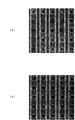
その後、図5(a)に示すように、SiN膜8、SiC膜5の露出部及びSiC膜3の露出部をエッチングにより除去する。このときのエッチング条件は、例えば、CHF3の流量:15sccm、CF4の流量:85sccm、圧力:13.3Pa(100mTorr)、RF電源パワー:300W、時間:30秒間、温度:25℃とする。この結果、ビアホール10がCu配線2まで到達すると共に、配線溝13がSiOC膜4まで到達する。また、主として配線溝13の側壁部に反応生成物14が付着する。反応生成物14は他の箇所にも付着するが、配線溝13の側壁部への付着量が最も多い。この反応生成物14は、SiC膜5の露出部が除去された後にSiOC膜4の極一部がエッチングされるために生じているものと考えられる。図7(a)は、反応生成物の生成状態を示すSEM(走査型電子顕微鏡)写真である。
【0029】
続いて、ビアホール10及び配線溝13の内部に対して酸素プラズマ処理を施す。このときの処理条件は、例えば、O2の流量:600sccm、圧力:40.0Pa(300mTorr)、RF電源パワー:300W、時間:60秒間、温度:25℃とする。この酸素プラズマ処理の結果、図5(b)に示すように、反応生成物14が除去される。図7(b)は、反応生成物が除去された状態を示すSEM(走査型電子顕微鏡)写真である。
【0030】
次に、ウェット処理として、フッ化アンモニウム又はリン酸アンモニウム等を含有する薬液を用いて全面を洗浄する。この結果、微細な残渣等が洗い流される。
【0031】
そして、図6に示すように、ビアホール10及び配線溝13内にCu配線15(配線材料)を埋め込む。その後、必要に応じて、更に層間絶縁膜及び配線等の形成を行い、半導体装置を完成させる。
【0032】
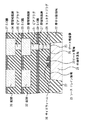
図8は、第1の実施形態を適用して製造した半導体装置の構造を示す断面図である。図8に示す例では、半導体基板21の表面に、素子分離領域22が形成され、この素子分離領域22により区画された素子活性領域内にトランジスタが形成されている。このトランジスタには、半導体基板21の表面に形成されたソース・ドレイン領域23、半導体基板21上に形成されたゲート絶縁膜24、ゲート絶縁膜24上に形成されたゲート電極25、及びゲート電極25の側方に形成されたサイドウォール26が設けられている。そして、このトランジスタを覆うようにして層間絶縁膜27が形成されている。層間絶縁膜27には、ソース・ドレイン領域23まで到達するコンタクトプラグ28が埋め込まれている。
【0033】
更に、全面にSiC膜29、層間絶縁膜30、SiC膜33、層間絶縁膜34及びSiC膜37が順次積層されている。そして、これらの膜にビアプラグ31、配線32、ビアプラグ35及び配線36が埋め込まれている。ビアプラグ31及び35が、図6中のCu配線15のビアホール10内に存在する部分に相当し、配線32及び36が、配線溝13内に存在する部分に相当する。このように、図8に示す例では、第1の実施形態に係る製造方法により、少なくとも2層の多層配線が形成されている。
【0034】
このように、第1の実施形態によれば、下層配線であるCu配線2の一部が露出した後で、Cu配線15を形成する前に、酸素プラズマ処理を行っているので、反応生成物14を除去することができる。このことは、図7(a)及び(b)を互いに比較することにより、明らかである。このため、その後に形成されるCu配線15とCu配線2とを良好な状態で接続させることができ、コンタクト不良及びコンタクト抵抗の増加を防止することができる。また、反応生成物14の残存に基づく信頼性の低下も防止することができる。そして、これらの結果、歩留りが向上する。
【0035】
なお、配線溝13を形成する工程(図4(a)参照)でも、反応生成物が生成されるが、この反応生成物はレジスト膜12及び樹脂材11を除去する際に除去される。
【0036】
(第2の実施形態)
次に、本発明の第2の実施形態について説明する。第2の実施形態は、本発明をシングルダマシン法に適用したものである。図9乃至図11は、本発明の第2の実施形態に係る半導体装置の製造方法を工程順に示す断面図である。
【0037】
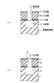
本実施形態では、先ず、第1の実施形態と同様に、Si基板等の半導体基板(図示せず)の表面にトランジスタ等の半導体素子(図示せず)を形成した後、半導体基板の上方に、図9(a)に示すように、層間絶縁膜1を形成する。次いで、この層間絶縁膜1に溝を形成し、その内部に、前記半導体素子に接続されるCu配線2を埋め込む。その後、層間絶縁膜1及びCu配線2上にSiC膜3、SiOC膜6、TEOS膜7及びSiN膜8を順次形成する。SiC膜3、SiOC膜6、TEOS膜7及びSiN膜8の各厚さは、夫々30nm乃至70nm、300nm乃至600nm、50nm乃至100nm、30nm乃至70nmである。続いて、配線用の開口部が設けられた配線用のレジスト膜12をSiN膜8上に形成する。レジスト膜12の厚さは、例えば500nm乃至800nm程度である。
【0038】
次に、図9(b)に示すように、レジスト膜12をマスクとして用いながら、SiN膜8、TEOS膜7及びSiOC膜6に配線溝13(開口部)を形成する。このときの各膜のエッチング条件は、次のとおりである。
【0039】
SiN膜8及びTEOS膜7のエッチングは、例えば、CF4の流量:100sccm、圧力:6.67Pa(50mTorr)、RF電源パワー:300W、時間:30秒間、温度:25℃の条件の下で連続して行う。
【0040】
SiOC膜6のエッチングは、先ず、例えば、CF4の流量:50sccm、CH2F2の流量:15sccm、O2の流量:5sccm、圧力:26.6Pa(200mTorr)、RF電源パワー:1000W、時間:30秒間、温度:25℃の条件の下で行う。次いで、SiOC膜6のエッチングが終了する前に、例えば、C4F6の流量:15sccm、O2の流量:30sccm、COの流量:500sccm、Arの流量:300sccm、圧力:5.33Pa(40mTorr)、RF電源パワー:1000W、時間:75秒間、温度:25℃の条件の下で行う。この条件では、SiOC膜6とSiC膜3との選択比が極めて大きく、SiC膜3はほとんどエッチングされない。
【0041】
配線溝13を形成した後、図10(a)に示すように、レジスト膜12をアッシングにより除去する。このときのアッシング条件は、例えば、O2の流量:250sccm、圧力:10.7Pa(80mTorr)、RF電源パワー:150W、時間:120秒間、温度:25℃とする。
【0042】
その後、図10(b)に示すように、SiC膜3の露出部及びSiN膜8をエッチングにより除去する。このときのエッチング条件は、例えば、CHF3の流量:15sccm、CF4の流量:85sccm、圧力:13.3Pa(100mTorr)、RF電源パワー:300W、時間:30秒間、温度:25℃とする。この結果、配線溝13がCu配線2まで到達する。また、配線溝13の側壁部に反応生成物14が付着する。
【0043】
続いて、反応生成物14に対して酸素プラズマ処理を施す。このときの処理条件は、例えば、O2の流量:600sccm、圧力:40.0Pa(300mTorr)、RF電源パワー:300W、時間:60秒間、温度:25℃とする。この酸素プラズマ処理の結果、図11(a)に示すように、反応生成物14が除去される。
【0044】
次に、ウェット処理として、フッ化アンモニウム又はリン酸アンモニウム等を含有する薬液を用いて全面を洗浄する。この結果、微細な残渣等が洗い流される。
【0045】
そして、図11(b)に示すように、配線溝13にCu配線16(配線材料)を埋め込む。その後、必要に応じて、更に層間絶縁膜及び配線等の形成を行い、半導体装置を完成させる。
【0046】
このような第2の実施形態によっても、反応生成物14を除去することができるため、第1の実施形態と同様の効果が得られる。
【0047】
なお、ウェット処理による洗浄を酸素プラズマ処理の前に行ってもよいが、微細な残渣等を除去するためには、ウェット処理を後に行うことが好ましい。
【0048】
また、酸素(O2)プラズマ処理の代わりに、水素を含有するガス、例えばN2及びH2の混合ガス、NH3ガス等のプラズマを用いた処理を行ってもよい。なお、いずれのプラズマを用いる場合であっても、半導体基板(ウェハ)が載置されるウェハステージの温度を120℃以下とすることが好ましい。これは、ウェハステージの温度が120℃を超えている場合には、Cu配線2の露出している部分に酸化等の変質が生じる虞があるからである。また、現状のプラズマ処理装置では、ウェハステージの温度を80℃以下に制御しやすく、更に、ウェハステージの温度が15℃未満となると結露が生じることがあるため、ウェハステージの温度を15℃以上80℃以下とすることがより好ましい。
【0049】
更に、第1の実施形態は、本発明を先ビア方式のデュアルダマシン法に適用したものであるが、本発明を先溝方式のデュアルダマシン法に適用することも可能である。この場合、ビアホールを下層配線まで到達させた後に、プラズマ処理を行えばよい。ウェット処理は、プラズマ処理の前でも後でもよいが、高い洗浄効果を得るためには、プラズマ処理の後に行うことが好ましい。
【0050】
また、拡散防止膜として、SiC膜3の代わりにSiN膜を用いてもよい。
【0051】
以下、本発明の諸態様を付記としてまとめて記載する。
【0052】
(付記1) ダマシン法により配線を形成する工程を有する半導体装置の製造方法において、
導電層上に、拡散防止膜及び層間絶縁膜を順次形成する工程と、
前記層間絶縁膜に前記拡散防止膜まで到達する開口部を形成する工程と、
前記拡散防止膜の前記層間絶縁膜に形成された開口部から露出する部分を除去するドライエッチングを行う工程と、
少なくとも前記開口部の内部に対して、酸素又は水素を含有するガスのプラズマを用いてプラズマ処理を行う工程と、
前記開口部内に配線材料を埋め込む工程と、
を有することを特徴とする半導体装置の製造方法。
【0053】
(付記2) 前記層間絶縁膜は、炭素原子を含有するシリコン酸化膜であることを特徴とする付記1に記載の半導体装置の製造方法。
【0054】
(付記3) 前記プラズマ処理を、前記導電層が形成されたウェハが載置されたステージの温度を120℃以下として行うことを特徴とする付記1又は2に記載の半導体装置の製造方法。
【0055】
(付記4) 前記プラズマ処理を、前記導電層が形成されたウェハが載置されたステージの温度を15℃以上80℃以下として行うことを特徴とする付記3に記載の半導体装置の製造方法。
【0056】
(付記5) 前記拡散防止膜は、前記導電層に含まれる金属元素が前記層間絶縁膜中に拡散することを防止する膜であることを特徴とする付記1乃至4のいずれか1項に記載の半導体装置の製造方法。
【0057】
(付記6) 前記拡散防止膜は、炭化シリコン膜又は窒化シリコン膜であることを特徴とする付記1乃至5のいずれか1項に記載の半導体装置の製造方法。
【0058】
(付記7) 前記層間絶縁膜を形成する工程と前記開口部を形成する工程との間に、前記層間絶縁膜の上に、エッチングストッパ膜及び第2の層間絶縁膜を順次形成する工程を有し、
前記開口部を形成する工程において、前記開口部を前記エッチングストッパ膜及び第2の層間絶縁膜をも貫通するものとし、
前記開口部を形成する工程と前記ドライエッチングを行う工程との間に、前記第2の層間絶縁膜に配線溝を形成する工程を有し、
前記ドライエッチングを行う工程において、前記エッチングストッパ膜の前記第2の層間絶縁膜に形成された配線溝から露出する部分を除去し、
前記プラズマ処理を行う工程において、前記配線溝の内部にもプラズマ処理を行い、
前記配線材料を埋め込む工程において、前記配線材料を前記配線溝内にも埋め込むことを特徴とする付記1乃至6のいずれか1項に記載の半導体装置の製造方法。
【0059】
(付記8) 前記第2の層間絶縁膜は、炭素原子を含有するシリコン酸化膜であることを特徴とする付記7に記載の半導体装置の製造方法。
【0060】
(付記9) 前記配線溝を形成する工程は、
前記開口部内に、前記層間絶縁膜よりも低い埋め込み材を埋め込む工程と、
マスクを用いて前記第2の層間絶縁膜をエッチングする工程と、
前記埋め込み材を除去する工程と、
を有することを特徴とする付記7又は8に記載の半導体装置の製造方法。
【0061】
(付記10) 前記導電層及び前記配線材料は、Cuを含有することを特徴とする付記1乃至9のいずれか1項に記載の半導体装置の製造方法。
【0062】
(付記11) 前記プラズマ処理を行う工程と前記配線材料を埋め込む工程との間に、前記導電層が形成されたウェハのウェット洗浄を行う工程を有することを特徴とする付記1乃至10のいずれか1項に記載の半導体装置の製造方法。
【0063】
(付記12) 前記ドライエッチングを行う工程と前記プラズマ処理を行う工程との間に、前記導電層が形成されたウェハのウェット洗浄を行う工程を有することを特徴とする付記1乃至10のいずれか1項に記載の半導体装置の製造方法。
【0064】
(付記13) 前記酸素又は水素を含有するガスとして、H2及びN2の混合ガス、NH3ガス、O2ガスから選択された1種のガスを用いることを特徴とする付記1乃至12のいずれか1項に記載の半導体装置の製造方法。
【0065】
(付記14) 前記開口部を形成する工程において、レジストマスクを用いることを特徴とする付記1乃至13のいずれか1項に記載の半導体装置の製造方法。
【0066】
(付記15) 前記プラズマ処理を行う工程の前に、前記レジストマスクをアッシングにより除去する工程を有することを特徴とする付記14に記載の半導体装置の製造方法。
【0067】
【発明の効果】
以上詳述したように、本発明によれば、プラズマ処理によってほぼ完全に反応生成物を除去することができ、その後に開口部に埋め込む配線材料と導電層とを確実に接続させることができる。このため、コンタクト抵抗の上昇を抑制することができる。また、反応生成物の除去により信頼性及び歩留りが向上する。
【図面の簡単な説明】
【図1】本発明の第1の実施形態に係る半導体装置の製造方法を工程順に示す断面図である。
【図2】図1に引き続き、第1の実施形態に係る半導体装置の製造方法を工程順に示す断面図である。
【図3】図2に引き続き、第1の実施形態に係る半導体装置の製造方法を工程順に示す断面図である。
【図4】図3に引き続き、第1の実施形態に係る半導体装置の製造方法を工程順に示す断面図である。
【図5】図4に引き続き、第1の実施形態に係る半導体装置の製造方法を工程順に示す断面図である。
【図6】図5に引き続き、第1の実施形態に係る半導体装置の製造方法を工程順に示す断面図である。
【図7】(a)は、反応生成物の生成状態を示す走査型電子顕微鏡写真であり、(b)は、反応生成物が除去された状態を示す走査型電子顕微鏡写真である。
【図8】第1の実施形態を適用して製造した半導体装置の構造を示す断面図である。
【図9】本発明の第2の実施形態に係る半導体装置の製造方法を工程順に示す断面図である。
【図10】図9に引き続き、第2の実施形態に係る半導体装置の製造方法を工程順に示す断面図である。
【図11】図10に引き続き、第2の実施形態に係る半導体装置の製造方法を工程順に示す断面図である。
【符号の説明】
1;層間絶縁膜
2、15、16;Cu配線
3、5;SiC膜
4、6;SiOC膜
7;TEOS膜
8;SiN膜
9、12;レジスト膜
10;ビアホール
11;樹脂材
13;配線溝
14;反応生成物[0001]
TECHNICAL FIELD OF THE INVENTION
The present invention relates to a method for manufacturing a semiconductor device suitable for forming a wiring layer.
[0002]
[Prior art]
With the demand for large-scale, high-integration and high-speed semiconductor integrated circuits, multilayer wiring materials having low resistance and interlayer insulating materials having small capacitance have been required. For this reason, aluminum (Al) alloy has been used as a multilayer wiring material and silicon (SiO) oxide has been used as an interlayer insulating film material. However, recently, in order to satisfy the above requirements, copper has been used as a wiring material. (Cu) is used, and a low dielectric material is used as an interlayer insulating film material.
[0003]
However, since fine processing of copper itself is very difficult, a damascene method is mainly used for forming copper wiring. The damascene method is a method in which after forming a groove pattern or a via hole pattern in an insulating film, a copper material is buried in these patterns, and then the copper material is polished (CMP: Chemical Mechanical Polishing) to form wiring. The damascene method includes a dual damascene method in which grooves and holes are formed at the same time, and a single damascene method in which these are individually formed.
[0004]
In many semiconductor devices, a plurality of wiring layers are formed, and a manufacturing process thereof requires a step of forming a via hole on a copper wiring. However, copper has a lower resistance to oxygen plasma as compared with an aluminum alloy which has been used as a wiring material until then. For this reason, when removing the resist mask used for forming the via hole, if the ashing conditions similar to those for the aluminum alloy are used as they are, there is a high possibility that a defect such as a contact failure will occur. Therefore, in order to avoid such a problem, a processing method that does not expose the surface of the copper wiring at the time of ashing has been constructed.
[0005]
In this processing method, a diffusion preventing film is formed between a copper wiring and an interlayer insulating film, and formation of a groove pattern or a via hole pattern in the interlayer insulating film is temporarily stopped by the diffusion preventing film. Then, the resist mask is removed by ashing, and thereafter, the diffusion prevention film is etched. According to such a method, since the surface of the copper wiring is hardly exposed to oxygen plasma, problems such as poor contact are prevented.
[0006]
However, at least the surface of the copper wiring is exposed when the diffusion prevention film is etched. For this reason, at this time (when the surface of the copper wiring is exposed), it is known that the reaction product adheres to the side wall portion of the groove pattern or the like. Therefore, conventionally, after the diffusion prevention film is etched as the last dry etching, a wet treatment using a chemical solution is performed to remove a reaction product.
[0007]
[Patent Document 1]
Japanese Patent Application Laid-Open No. H11-31669 [Patent Document 2]
JP 2001-284327 A
[Problems to be solved by the invention]
However, when the SiO 2 film is used as an interlayer insulating film, no particular problem has occurred in the above-described conventional method, but recently, when an SiOC film is used as an interlayer insulating film having a lower dielectric constant, The contact resistance increases, the yield decreases, and the reliability decreases.
[0009]
The present invention has been made in view of such a problem, and a semiconductor device capable of suppressing an increase in contact resistance, a decrease in yield, and a decrease in reliability even when an SiOC film is used as an interlayer insulating film. It is an object of the present invention to provide a method for producing the same.
[0010]
[Means for Solving the Problems]
The inventor of the present application has conducted intensive studies in order to solve the above-described problems. As a result, when an insulating film containing C such as a SiOC film is used as an interlayer insulating film, the amount of a reaction product is reduced by using an SiO 2 film. It has been found that the reaction product cannot be sufficiently removed only by performing the conventional wet treatment as compared with the case where the conventional method is used. The inventor of the present application has also found that the remaining reaction product collapses into a via hole or the like that has already been formed and hinders formation of a copper wiring later. Therefore, experiments were performed using various chemicals to remove the reaction products by wet treatment, but the reaction products were completely removed without adversely affecting the surface of the copper wiring and the low dielectric film (interlayer insulating film). I couldn't.
[0011]
Then, as a result of further intense study, the inventor of the present application has come up with various aspects of the invention described below.
[0012]
A method of manufacturing a semiconductor device according to the present invention is directed to a method of manufacturing a semiconductor device having a step of forming a wiring by a damascene method. Then, in this manufacturing method, first, a diffusion preventing film and an interlayer insulating film are sequentially formed on the conductive layer. Next, an opening reaching the diffusion preventing film is formed in the interlayer insulating film. Next, dry etching is performed to remove a portion of the diffusion barrier film exposed from the opening formed in the interlayer insulating film. Thereafter, plasma processing is performed on at least the inside of the opening using a plasma of a gas containing oxygen or hydrogen. Then, a wiring material is embedded in the opening.
[0013]
In the present invention, after the diffusion preventing film is selectively removed by dry etching, and before the wiring material is buried in the opening, a plasma treatment using a plasma of a gas containing oxygen or hydrogen is performed. Therefore, even when a large amount of reaction products adhere to the side walls of the opening by dry etching using the SiOC film as an interlayer insulating film, the reaction products can be almost completely removed by plasma treatment. is there. As a result, it is possible to avoid problems such as defective wiring formation and reduced reliability.
[0014]
BEST MODE FOR CARRYING OUT THE INVENTION
Hereinafter, a method for manufacturing a semiconductor device according to an embodiment of the present invention will be specifically described with reference to the accompanying drawings.
[0015]
(1st Embodiment)
First, a first embodiment of the present invention will be described. In the first embodiment, the invention of the present application is applied to a dual damascene method using a via-via method. 1 to 6 are sectional views showing a method of manufacturing a semiconductor device according to the first embodiment of the present invention in the order of steps.
[0016]
In the present embodiment, first, after a semiconductor element (not shown) such as a transistor is formed on a surface of a semiconductor substrate (not shown) such as a Si substrate, as shown in FIG. Next, an interlayer insulating film 1 is formed. Next, a groove is formed in the interlayer insulating film 1 and a
[0017]
Subsequently, as shown in FIG. 1B, a resist
[0018]
Next, as shown in FIG. 2A, via holes 10 (openings) are formed in the
[0019]
The etching of the
[0020]
The
[0021]
The
[0022]
After forming the via holes 10, the resist
[0023]
Next, as shown in FIG. 2B, a
[0024]
Thereafter, as shown in FIG. 3A, the entire surface of the
[0025]
Subsequently, as shown in FIG. 3B, a resist
[0026]
Next, as shown in FIG. 4A, a
[0027]
Next, as shown in FIG. 4B, the resist
[0028]
Thereafter, as shown in FIG. 5A, the exposed portions of the
[0029]
Subsequently, the inside of the via
[0030]
Next, as a wet treatment, the entire surface is washed using a chemical solution containing ammonium fluoride, ammonium phosphate, or the like. As a result, fine residues and the like are washed away.
[0031]
Then, as shown in FIG. 6, a Cu wiring 15 (wiring material) is buried in the via
[0032]
FIG. 8 is a cross-sectional view illustrating a structure of a semiconductor device manufactured by applying the first embodiment. In the example shown in FIG. 8, an
[0033]
Further, an SiC film 29, an interlayer insulating film 30, a SiC film 33, an interlayer insulating film 34, and a SiC film 37 are sequentially stacked on the entire surface. The via plug 31, the wiring 32, the via plug 35, and the wiring 36 are embedded in these films. The via plugs 31 and 35 correspond to portions existing in the via
[0034]
As described above, according to the first embodiment, the oxygen plasma treatment is performed before the Cu wiring 15 is formed after a portion of the
[0035]
In the step of forming the wiring groove 13 (see FIG. 4A), a reaction product is also generated. The reaction product is removed when the resist
[0036]
(Second embodiment)
Next, a second embodiment of the present invention will be described. In the second embodiment, the present invention is applied to a single damascene method. 9 to 11 are sectional views showing a method of manufacturing a semiconductor device according to the second embodiment of the present invention in the order of steps.
[0037]
In the present embodiment, first, similarly to the first embodiment, after a semiconductor element (not shown) such as a transistor is formed on a surface of a semiconductor substrate (not shown) such as a Si substrate, Then, as shown in FIG. 9A, an interlayer insulating film 1 is formed. Next, a groove is formed in the interlayer insulating film 1 and a
[0038]
Next, as shown in FIG. 9B, a wiring groove 13 (opening) is formed in the
[0039]
The etching of the
[0040]
First, the
[0041]
After forming the
[0042]
Thereafter, as shown in FIG. 10B, the exposed portion of the
[0043]
Subsequently, the reaction product 14 is subjected to an oxygen plasma treatment. The processing conditions at this time are, for example, O 2 flow rate: 600 sccm, pressure: 40.0 Pa (300 mTorr), RF power supply power: 300 W, time: 60 seconds, temperature: 25 ° C. As a result of this oxygen plasma treatment, the reaction product 14 is removed as shown in FIG.
[0044]
Next, as a wet treatment, the entire surface is washed using a chemical solution containing ammonium fluoride, ammonium phosphate, or the like. As a result, fine residues and the like are washed away.
[0045]
Then, as shown in FIG. 11B, a Cu wiring 16 (wiring material) is buried in the
[0046]
According to the second embodiment, the reaction product 14 can be removed, and the same effect as that of the first embodiment can be obtained.
[0047]
Note that the cleaning by wet treatment may be performed before the oxygen plasma treatment, but it is preferable to perform the wet treatment afterward in order to remove fine residues and the like.
[0048]
Instead of the oxygen (O 2 ) plasma treatment, a treatment using a plasma containing a gas containing hydrogen, for example, a mixed gas of N 2 and H 2 or an NH 3 gas may be performed. Regardless of the type of plasma used, the temperature of the wafer stage on which the semiconductor substrate (wafer) is mounted is preferably set to 120 ° C. or lower. This is because if the temperature of the wafer stage exceeds 120 ° C., the exposed portion of the
[0049]
Further, in the first embodiment, the present invention is applied to the dual damascene method of the via-via method, but the present invention can also be applied to the dual damascene method of the forward groove method. In this case, the plasma processing may be performed after the via hole reaches the lower wiring. The wet treatment may be performed before or after the plasma treatment, but is preferably performed after the plasma treatment in order to obtain a high cleaning effect.
[0050]
Further, a SiN film may be used instead of the
[0051]
Hereinafter, various aspects of the present invention will be collectively described as supplementary notes.
[0052]
(Supplementary Note 1) In a method of manufacturing a semiconductor device having a step of forming a wiring by a damascene method,
A step of sequentially forming a diffusion prevention film and an interlayer insulating film on the conductive layer,
Forming an opening reaching the diffusion barrier film in the interlayer insulating film;
Performing dry etching to remove a portion of the diffusion prevention film exposed from an opening formed in the interlayer insulating film;
At least for the inside of the opening, a step of performing a plasma treatment using a plasma of a gas containing oxygen or hydrogen,
Embedding a wiring material in the opening;
A method for manufacturing a semiconductor device, comprising:
[0053]
(Supplementary Note 2) The method of Supplementary Note 1, wherein the interlayer insulating film is a silicon oxide film containing carbon atoms.
[0054]
(Supplementary Note 3) The method for producing a semiconductor device according to
[0055]
(Supplementary Note 4) The method for manufacturing a semiconductor device according to
[0056]
(Supplementary note 5) The non-diffusion film according to any one of Supplementary notes 1 to 4, wherein the diffusion prevention film is a film that prevents a metal element included in the conductive layer from diffusing into the interlayer insulating film. Manufacturing method of a semiconductor device.
[0057]
(Supplementary Note 6) The method of manufacturing a semiconductor device according to any one of Supplementary Notes 1 to 5, wherein the diffusion prevention film is a silicon carbide film or a silicon nitride film.
[0058]
(Supplementary Note 7) Between the step of forming the interlayer insulating film and the step of forming the opening, a step of sequentially forming an etching stopper film and a second interlayer insulating film on the interlayer insulating film is provided. And
In the step of forming the opening, the opening penetrates the etching stopper film and the second interlayer insulating film,
Forming a wiring groove in the second interlayer insulating film between the step of forming the opening and the step of performing the dry etching;
In the step of performing the dry etching, removing a portion of the etching stopper film exposed from a wiring groove formed in the second interlayer insulating film;
In the step of performing the plasma processing, plasma processing is also performed inside the wiring groove,
7. The method of manufacturing a semiconductor device according to claim 1, wherein in the step of embedding the wiring material, the wiring material is embedded also in the wiring groove.
[0059]
(Supplementary Note 8) The method for manufacturing a semiconductor device according to
[0060]
(Supplementary Note 9) The step of forming the wiring groove includes:
Burying a filling material lower than the interlayer insulating film in the opening;
Etching the second interlayer insulating film using a mask;
Removing the embedding material;
9. The method for manufacturing a semiconductor device according to
[0061]
(Supplementary Note 10) The method of manufacturing a semiconductor device according to any one of Supplementary Notes 1 to 9, wherein the conductive layer and the wiring material contain Cu.
[0062]
(Supplementary Note 11) Any of the supplementary notes 1 to 10, further comprising a step of performing wet cleaning of the wafer on which the conductive layer is formed, between the step of performing the plasma processing and the step of embedding the wiring material. 2. The method for manufacturing a semiconductor device according to claim 1.
[0063]
(Supplementary Note 12) Any of the supplementary notes 1 to 10, further comprising a step of performing wet cleaning of the wafer on which the conductive layer is formed, between the step of performing the dry etching and the step of performing the plasma processing. 2. The method for manufacturing a semiconductor device according to claim 1.
[0064]
(Supplementary Note 13) As the gas containing oxygen or hydrogen, a gas selected from a mixed gas of H 2 and N 2 , NH 3 gas, and O 2 gas is used. A method for manufacturing the semiconductor device according to claim 1.
[0065]
(Supplementary Note 14) The method of manufacturing a semiconductor device according to any one of Supplementary Notes 1 to 13, wherein a resist mask is used in the step of forming the opening.
[0066]
(Supplementary Note 15) The method of manufacturing a semiconductor device according to Supplementary Note 14, further comprising a step of removing the resist mask by ashing before the step of performing the plasma processing.
[0067]
【The invention's effect】
As described in detail above, according to the present invention, the reaction product can be almost completely removed by the plasma treatment, and the wiring material to be embedded in the opening and the conductive layer can be reliably connected thereafter. Therefore, an increase in contact resistance can be suppressed. Further, the reliability and the yield are improved by removing the reaction products.
[Brief description of the drawings]
FIG. 1 is a sectional view illustrating a method for manufacturing a semiconductor device according to a first embodiment of the present invention in the order of steps.
FIG. 2 is a cross-sectional view showing a method of manufacturing the semiconductor device according to the first embodiment in order of steps, following FIG. 1;
FIG. 3 is a cross-sectional view showing a method of manufacturing the semiconductor device according to the first embodiment in the order of steps, following FIG. 2;
FIG. 4 is a cross-sectional view illustrating the method of manufacturing the semiconductor device according to the first embodiment in the order of steps, following FIG. 3;
FIG. 5 is a cross-sectional view showing the method of manufacturing the semiconductor device according to the first embodiment in the order of steps, following FIG. 4;
FIG. 6 is a cross-sectional view showing the method of manufacturing the semiconductor device according to the first embodiment in the order of steps, following FIG. 5;
FIG. 7 (a) is a scanning electron micrograph showing the state of production of a reaction product, and FIG. 7 (b) is a scanning electron micrograph showing the state where the reaction product has been removed.
FIG. 8 is a cross-sectional view illustrating a structure of a semiconductor device manufactured by applying the first embodiment.
FIG. 9 is a sectional view illustrating a method for manufacturing a semiconductor device according to a second embodiment of the present invention in the order of steps.
FIG. 10 is a cross-sectional view showing a method of manufacturing the semiconductor device according to the second embodiment in the order of steps, following FIG. 9;
FIG. 11 is a cross-sectional view showing a method of manufacturing the semiconductor device according to the second embodiment in the order of steps, following FIG. 10;
[Explanation of symbols]
1;
Claims (10)
導電層上に、拡散防止膜及び層間絶縁膜を順次形成する工程と、
前記層間絶縁膜に前記拡散防止膜まで到達する開口部を形成する工程と、
前記拡散防止膜の前記層間絶縁膜に形成された開口部から露出する部分を除去するドライエッチングを行う工程と、
少なくとも前記開口部の内部に対して、酸素又は水素を含有するガスのプラズマを用いてプラズマ処理を行う工程と、
前記開口部内に配線材料を埋め込む工程と、
を有することを特徴とする半導体装置の製造方法。In a method of manufacturing a semiconductor device having a step of forming wiring by a damascene method,
A step of sequentially forming a diffusion prevention film and an interlayer insulating film on the conductive layer,
Forming an opening reaching the diffusion barrier film in the interlayer insulating film;
Performing dry etching to remove a portion of the diffusion prevention film exposed from an opening formed in the interlayer insulating film;
At least for the inside of the opening, a step of performing a plasma treatment using a plasma of a gas containing oxygen or hydrogen,
Embedding a wiring material in the opening;
A method for manufacturing a semiconductor device, comprising:
前記開口部を形成する工程において、前記開口部を前記エッチングストッパ膜及び第2の層間絶縁膜をも貫通するものとし、
前記開口部を形成する工程と前記ドライエッチングを行う工程との間に、前記第2の層間絶縁膜に配線溝を形成する工程を有し、
前記ドライエッチングを行う工程において、前記エッチングストッパ膜の前記第2の層間絶縁膜に形成された配線溝から露出する部分を除去し、
前記プラズマ処理を行う工程において、前記配線溝の内部にもプラズマ処理を行い、
前記配線材料を埋め込む工程において、前記配線材料を前記配線溝内にも埋め込むことを特徴とする請求項1乃至4のいずれか1項に記載の半導体装置の製造方法。A step of sequentially forming an etching stopper film and a second interlayer insulating film on the interlayer insulating film between the step of forming the interlayer insulating film and the step of forming the opening;
In the step of forming the opening, the opening penetrates the etching stopper film and the second interlayer insulating film,
Forming a wiring groove in the second interlayer insulating film between the step of forming the opening and the step of performing the dry etching;
In the step of performing the dry etching, removing a portion of the etching stopper film exposed from a wiring groove formed in the second interlayer insulating film;
In the step of performing the plasma processing, plasma processing is also performed inside the wiring groove,
5. The method of manufacturing a semiconductor device according to claim 1, wherein, in the step of embedding the wiring material, the wiring material is also embedded in the wiring groove.
Priority Applications (2)
| Application Number | Priority Date | Filing Date | Title |
|---|---|---|---|
| JP2003049868A JP3781729B2 (en) | 2003-02-26 | 2003-02-26 | Manufacturing method of semiconductor device |
| US10/768,074 US6881661B2 (en) | 2003-02-26 | 2004-02-02 | Manufacturing method of semiconductor device |
Applications Claiming Priority (1)
| Application Number | Priority Date | Filing Date | Title |
|---|---|---|---|
| JP2003049868A JP3781729B2 (en) | 2003-02-26 | 2003-02-26 | Manufacturing method of semiconductor device |
Publications (2)
| Publication Number | Publication Date |
|---|---|
| JP2004260001A true JP2004260001A (en) | 2004-09-16 |
| JP3781729B2 JP3781729B2 (en) | 2006-05-31 |
Family
ID=32923325
Family Applications (1)
| Application Number | Title | Priority Date | Filing Date |
|---|---|---|---|
| JP2003049868A Expired - Fee Related JP3781729B2 (en) | 2003-02-26 | 2003-02-26 | Manufacturing method of semiconductor device |
Country Status (2)
| Country | Link |
|---|---|
| US (1) | US6881661B2 (en) |
| JP (1) | JP3781729B2 (en) |
Cited By (6)
| Publication number | Priority date | Publication date | Assignee | Title |
|---|---|---|---|---|
| JP2004296835A (en) * | 2003-03-27 | 2004-10-21 | Applied Materials Inc | Method for constructing damascene structure |
| JP2007059759A (en) * | 2005-08-26 | 2007-03-08 | Victor Co Of Japan Ltd | Method of manufacturing semiconductor laser device |
| JP2010161166A (en) * | 2009-01-07 | 2010-07-22 | Fujitsu Semiconductor Ltd | Method of forming interconnection |
| US8125084B2 (en) | 2006-10-12 | 2012-02-28 | Rohm Co., Ltd. | Semiconductor device and semiconductor device manufacturing method |
| JP2015002193A (en) * | 2013-06-13 | 2015-01-05 | キヤノン株式会社 | Method for manufacturing electronic device |
| KR20170009686A (en) * | 2015-07-17 | 2017-01-25 | 타이완 세미콘덕터 매뉴팩쳐링 컴퍼니 리미티드 | Method for cleaning via of interconnect structure of semiconductor device structure |
Families Citing this family (4)
| Publication number | Priority date | Publication date | Assignee | Title |
|---|---|---|---|---|
| JP4619747B2 (en) * | 2004-11-01 | 2011-01-26 | 株式会社東芝 | Manufacturing method of semiconductor device |
| JP4197691B2 (en) * | 2005-06-21 | 2008-12-17 | 株式会社東芝 | Manufacturing method of semiconductor device |
| JPWO2017037828A1 (en) * | 2015-08-31 | 2018-06-14 | オリンパス株式会社 | Endoscope, electronic unit, and method of manufacturing electronic unit |
| JP6945385B2 (en) * | 2017-08-14 | 2021-10-06 | 東京エレクトロン株式会社 | Plasma processing method and plasma processing equipment |
Family Cites Families (7)
| Publication number | Priority date | Publication date | Assignee | Title |
|---|---|---|---|---|
| TW410455B (en) * | 1998-02-16 | 2000-11-01 | United Microelectronics Corp | Forming method for dual damascene structure |
| US6127089A (en) * | 1998-08-28 | 2000-10-03 | Advanced Micro Devices, Inc. | Interconnect structure with low k dielectric materials and method of making the same with single and dual damascene techniques |
| KR100300065B1 (en) * | 1999-01-20 | 2002-01-19 | 김영환 | Method of forming interconnection for semiconductor device |
| US6211069B1 (en) * | 1999-05-17 | 2001-04-03 | Taiwan Semiconductor Manufacturing Company | Dual damascene process flow for a deep sub-micron technology |
| US6358842B1 (en) * | 2000-08-07 | 2002-03-19 | Chartered Semiconductor Manufacturing Ltd. | Method to form damascene interconnects with sidewall passivation to protect organic dielectrics |
| TW567554B (en) * | 2001-08-08 | 2003-12-21 | Lam Res Corp | All dual damascene oxide etch process steps in one confined plasma chamber |
| US6809028B2 (en) * | 2002-10-29 | 2004-10-26 | Taiwan Semiconductor Manufacturing Company, Ltd. | Chemistry for liner removal in a dual damascene process |
-
2003
- 2003-02-26 JP JP2003049868A patent/JP3781729B2/en not_active Expired - Fee Related
-
2004
- 2004-02-02 US US10/768,074 patent/US6881661B2/en not_active Expired - Lifetime
Cited By (8)
| Publication number | Priority date | Publication date | Assignee | Title |
|---|---|---|---|---|
| JP2004296835A (en) * | 2003-03-27 | 2004-10-21 | Applied Materials Inc | Method for constructing damascene structure |
| JP2007059759A (en) * | 2005-08-26 | 2007-03-08 | Victor Co Of Japan Ltd | Method of manufacturing semiconductor laser device |
| US8125084B2 (en) | 2006-10-12 | 2012-02-28 | Rohm Co., Ltd. | Semiconductor device and semiconductor device manufacturing method |
| JP2010161166A (en) * | 2009-01-07 | 2010-07-22 | Fujitsu Semiconductor Ltd | Method of forming interconnection |
| JP2015002193A (en) * | 2013-06-13 | 2015-01-05 | キヤノン株式会社 | Method for manufacturing electronic device |
| KR20170009686A (en) * | 2015-07-17 | 2017-01-25 | 타이완 세미콘덕터 매뉴팩쳐링 컴퍼니 리미티드 | Method for cleaning via of interconnect structure of semiconductor device structure |
| US9761488B2 (en) | 2015-07-17 | 2017-09-12 | Taiwan Semiconductor Manufacturing Company, Ltd. | Method for cleaning via of interconnect structure of semiconductor device structure |
| KR101898764B1 (en) * | 2015-07-17 | 2018-09-13 | 타이완 세미콘덕터 매뉴팩쳐링 컴퍼니 리미티드 | Method for cleaning via of interconnect structure of semiconductor device structure |
Also Published As
| Publication number | Publication date |
|---|---|
| JP3781729B2 (en) | 2006-05-31 |
| US6881661B2 (en) | 2005-04-19 |
| US20040175931A1 (en) | 2004-09-09 |
Similar Documents
| Publication | Publication Date | Title |
|---|---|---|
| JP3248492B2 (en) | Semiconductor device and manufacturing method thereof | |
| US7871923B2 (en) | Self-aligned air-gap in interconnect structures | |
| US7419916B2 (en) | Manufacturing method of semiconductor device | |
| US20050214694A1 (en) | Pattern formation method | |
| US8513114B2 (en) | Method for forming a dual damascene interconnect structure | |
| JP2005072384A (en) | Method for manufacturing electronic device | |
| JP4256347B2 (en) | Manufacturing method of semiconductor device | |
| JPWO2004061931A1 (en) | Semiconductor device having multilayer wiring structure and method for manufacturing the same | |
| KR100641502B1 (en) | Method for forming a contact using dual damascene process in semiconductor fabrication | |
| JP3781729B2 (en) | Manufacturing method of semiconductor device | |
| JP2005116801A (en) | Method for manufacturing semiconductor device | |
| US20040150075A1 (en) | Semiconductor device with cupper wiring and method for manufacturing semiconductor device | |
| JPWO2007043634A1 (en) | Manufacturing method of multilayer wiring | |
| US7384823B2 (en) | Method for manufacturing a semiconductor device having a stabilized contact resistance | |
| JP2004282082A (en) | Metal burying method | |
| US7338897B2 (en) | Method of fabricating a semiconductor device having metal wiring | |
| US20220102143A1 (en) | Metal Hard Masks for Reducing Line Bending | |
| JP2005005697A (en) | Manufacturing method of semiconductor device | |
| JP2006156591A (en) | Method for manufacturing semiconductor device | |
| JP4948278B2 (en) | Manufacturing method of semiconductor device | |
| JPH1167909A (en) | Manufacture of semiconductor device | |
| JP4436606B2 (en) | Manufacturing method of semiconductor device | |
| KR100483838B1 (en) | Dual damascene process of metal wire | |
| JP3746231B2 (en) | Method for removing via bottom insulating film and method for manufacturing semiconductor device | |
| KR100737701B1 (en) | Method of manufacturing wire in a semiconductor device |
Legal Events
| Date | Code | Title | Description |
|---|---|---|---|
| A621 | Written request for application examination |
Free format text: JAPANESE INTERMEDIATE CODE: A621 Effective date: 20040726 |
|
| A977 | Report on retrieval |
Free format text: JAPANESE INTERMEDIATE CODE: A971007 Effective date: 20051118 |
|
| A131 | Notification of reasons for refusal |
Free format text: JAPANESE INTERMEDIATE CODE: A131 Effective date: 20051129 |
|
| A521 | Written amendment |
Free format text: JAPANESE INTERMEDIATE CODE: A523 Effective date: 20060127 |
|
| TRDD | Decision of grant or rejection written | ||
| A01 | Written decision to grant a patent or to grant a registration (utility model) |
Free format text: JAPANESE INTERMEDIATE CODE: A01 Effective date: 20060221 |
|
| A61 | First payment of annual fees (during grant procedure) |
Free format text: JAPANESE INTERMEDIATE CODE: A61 Effective date: 20060307 |
|
| R150 | Certificate of patent or registration of utility model |
Ref document number: 3781729 Country of ref document: JP Free format text: JAPANESE INTERMEDIATE CODE: R150 Free format text: JAPANESE INTERMEDIATE CODE: R150 |
|
| S111 | Request for change of ownership or part of ownership |
Free format text: JAPANESE INTERMEDIATE CODE: R313111 |
|
| FPAY | Renewal fee payment (event date is renewal date of database) |
Free format text: PAYMENT UNTIL: 20090317 Year of fee payment: 3 |
|
| R350 | Written notification of registration of transfer |
Free format text: JAPANESE INTERMEDIATE CODE: R350 |
|
| FPAY | Renewal fee payment (event date is renewal date of database) |
Free format text: PAYMENT UNTIL: 20100317 Year of fee payment: 4 |
|
| FPAY | Renewal fee payment (event date is renewal date of database) |
Free format text: PAYMENT UNTIL: 20100317 Year of fee payment: 4 |
|
| FPAY | Renewal fee payment (event date is renewal date of database) |
Free format text: PAYMENT UNTIL: 20110317 Year of fee payment: 5 |
|
| FPAY | Renewal fee payment (event date is renewal date of database) |
Free format text: PAYMENT UNTIL: 20110317 Year of fee payment: 5 |
|
| S531 | Written request for registration of change of domicile |
Free format text: JAPANESE INTERMEDIATE CODE: R313531 |
|
| S533 | Written request for registration of change of name |
Free format text: JAPANESE INTERMEDIATE CODE: R313533 |
|
| FPAY | Renewal fee payment (event date is renewal date of database) |
Free format text: PAYMENT UNTIL: 20110317 Year of fee payment: 5 |
|
| R350 | Written notification of registration of transfer |
Free format text: JAPANESE INTERMEDIATE CODE: R350 |
|
| FPAY | Renewal fee payment (event date is renewal date of database) |
Free format text: PAYMENT UNTIL: 20110317 Year of fee payment: 5 |
|
| FPAY | Renewal fee payment (event date is renewal date of database) |
Free format text: PAYMENT UNTIL: 20120317 Year of fee payment: 6 |
|
| FPAY | Renewal fee payment (event date is renewal date of database) |
Free format text: PAYMENT UNTIL: 20130317 Year of fee payment: 7 |
|
| FPAY | Renewal fee payment (event date is renewal date of database) |
Free format text: PAYMENT UNTIL: 20140317 Year of fee payment: 8 |
|
| S531 | Written request for registration of change of domicile |
Free format text: JAPANESE INTERMEDIATE CODE: R313531 |
|
| R350 | Written notification of registration of transfer |
Free format text: JAPANESE INTERMEDIATE CODE: R350 |
|
| LAPS | Cancellation because of no payment of annual fees |