JP3668356B2 - Fast Fourier transform circuit - Google Patents
Fast Fourier transform circuit Download PDFInfo
- Publication number
- JP3668356B2 JP3668356B2 JP08799997A JP8799997A JP3668356B2 JP 3668356 B2 JP3668356 B2 JP 3668356B2 JP 08799997 A JP08799997 A JP 08799997A JP 8799997 A JP8799997 A JP 8799997A JP 3668356 B2 JP3668356 B2 JP 3668356B2
- Authority
- JP
- Japan
- Prior art keywords
- circuit
- fourier transform
- fast fourier
- radix
- data
- Prior art date
- Legal status (The legal status is an assumption and is not a legal conclusion. Google has not performed a legal analysis and makes no representation as to the accuracy of the status listed.)
- Expired - Lifetime
Links
Images


Landscapes
- Complex Calculations (AREA)
Description
【0001】
【発明の属する技術分野】
本発明は、信号処理、データ解析、線形システム等に利用される高速フーリエ変換に係り、特に、入力データ点数Nに対して、入力データ点数が減少しても、高速フーリエ変換(以下、FFTと略称する)が行える高速フーリエ変換演算回路に関するものである。
【0002】
【従来の技術】
近年のディジタル技術の発展に伴い、地上波テレビ放送が現行のアナログ放送からディジタル放送へ移行しようと準備が行われている。この地上波ディジタルテレビ放送では変調方式としてマルチキャリア直交周波数分割多重変調方式(以下、OFDMと略称する)の採用が見込まれている。このOFDMでは搬送波の変復調に高速フーリエ変換が用いられている。この変調方式で用いられる高速フーリエ変換の高速フーリエ変換点数NはOFDMの搬送波数Kに依存する。
【0003】
この搬送波数Kは規格上では1705本、6817本、と様々であり、また、これらの規格はさらに増える可能性がある。これらの複数の搬送波の本数に対応させるためにはそれぞれ専用の高速フーリエ変換演算回路を用意する必要があった。また、従来存在している複数のデータ点数に対応可能な高速フーリエ変換演算回路は点数Nに対してN/R、N/R2、(Rは基数)…というようにRのべき乗で分割された点数しか計算できない。
【0004】
また、異なる基数のバタフライ演算回路を持たせることで、多くの点数に対応した高速フーリエ変換回路も存在するが、この場合に全ての並べ替え回路の構造を変更する必要があり、演算回路の制御が困難になる。したがってRに関係なく同一の回路で様々な点数に対応することができ、かつ、データ点列の変更に対しての制御が容易な回路は存在していない。
【0005】
【発明が解決しようとする課題】
前述のように、従来の高速フーリエ変換を行う回路では点数Nが決定されると、回路構成も一意に定まってしまう。したがって、入力データの点数が変更になり、減少しても同一の回路で演算を行うことができないという問題点があった。
【0006】
また、点数を可変にすることのできる高速フーリエ変換演算回路でも点数の変更は基数Rのべき乗分の1でしか変更することができない。即ち、点数の変更が基数Rに左右されるという問題点があった。
【0007】
本発明は、上記従来の欠点に鑑み、入力データ点数が減少しても、基数Rに左右されることなく変換点数を設定し、同一の回路で変換が行える回路を提供することを目的とするものである。
【0008】
【課題を解決するための手段】
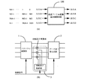
図1は本発明の原理を説明する図であり、図1(a)は基本回路へのデータ入力の概念を示し、図1(b)は本発明の基本回路の構成例を示している。図2は本発明におけるバタフライ演算回路の構成例を示し、図3はデータ並べ替え回路の構成例を示している。上記の問題点は下記の如く構成した高速フーリエ変換回路によって解決される。
【0009】
(1)処理する高速フーリエ変換(FFT)点数Nについて、高速フーリエ変換を行う回路であって、バタフライ演算部1、回転因子乗算部3、データ並べ替え回路2からなるR入力の基本演算回路100を1段として、これをM個(=logRN)(Rは基数)直列に並べて高速フーリエ変換が行えるように構成し、バタフライ演算部1では、上記R入力間で基数Rのたすき掛け演算を行い、回転因子乗算部3では、バタフライ演算部2の出力のうちR−1個の出力に対して回転因子の乗算を行い、データ並べ替え回路2では、上記入力データNに対し2段目以降の演算に必要となるデータの組を生成し、さらに、外部からの制御信号により、バタフライ演算部1の基数が変更可能であり、回転因子乗算部3および、データ並べ替え回路2を基数に応じて変更できる基本演算回路100を1個もしくは複数個備え、そのうち、1個もしくは複数個の基本演算回路100の基数を変更することで、上記高速フーリエ変換点数Nが基数Rに関わりなくN/2、N/4、…となっても同一の回路で高速フーリエ変換を行う。
【0010】
(2)(1)に示した高速フーリエ変換演算回路であり、バタフライ演算の途中経過を出力する信号線を備え、選択回路5により、前記信号線の信号とほかの計算結果が選択できるバタフライ演算部1を備え、外部からの信号により、基数の変更を可能にした。
【0011】
(3)(1)に示した高速フーリエ変換回路であり、基本演算回路100におけるデータ並べ替え回路で、入力段に複数の遅延量が可変な遅延素子6,7,8を備え、基数に応じて切り替え状態を変更できるスイッチ回路9を備え、出力段に複数の遅延量が可変の遅延素子6,7,8を備え、外部からの制御信号に基づいて基数が変更に対応することが可能なデータ並べ替え回路を持つ。
【0012】
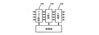
(4)(1)に示した高速フーリエ変換演算回路であり、M段の基本演算回路100を直列に接続した回路において、前方からL段(L≦M)を基数が変更可能な基本演算回路とする。
【0013】
(5)(1)に示した高速フーリエ変換演算回路であり、全ての基本演算回路100を基数が変更可能な演算回路とし、すべての基本演算回路100で基数をRより小さく、同一の値に設定し、請求項3におけるデータ並べ替え回路2において、遅延量を変更できる遅延素子6,8の遅延量を等しくし、外部からの制御信号に基づいてそれぞれ独立した入力データをフーリエ変換し出力することが可能なもの。
【0015】
以上の構成において更に、処理する高速フーリエ変換(FFT)点数Nについて、高速フーリエ変換を行う回路であって、バタフライ演算部1、回転因子乗算部3、データ並べ替え回路 2からなる基本演算回路100を複数個並べることで構成する。このうち1個もしくは複数個の基本演算回路100のバタフライ演算部1を基数が変更可能な回路構成にする。この演算回路に入力データを適切に入力することでN点の高速フーリエ変換の結果が得られる。
【0016】
このとき、1個もしくは複数個のバタフライ演算部1の基数を変更することで、基数Rに関係することなくフレキシブルにN/2、N/4、…、2点の高速フーリエ変換が可能となる。さらに、この演算回路を用いることで、これまでに高速フーリエ変換点数ごとに必要となっていた演算回路がただ一つの演算回路でよくなるので、ハードウェアの削減ができる。また、地上波ディジタル放送の種々の伝送パラメータに対応でき、受信システムを瞬時に切り替えることができる。
【0017】
本発明によると、ハードウェアの大幅な増大なしに複数のデータ点列数に対応した高速フーリエ変換が可能である。また、本発明の構成によると、独立した2つのデータを高速にフーリエ変換できる。
【0018】
【発明の実施の形態】
以下、本発明の実施の形態について図面を用いて詳細に説明する。図1〜図3は本発明の原理を説明する図であり、図4〜図12は本発明の実施の形態を示した図である。図13は従来の高速フーリエ変換を説明する図であり、図14〜図16は本発明の他の実施の形態を示している。
【0019】
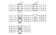
本発明において、高速フーリエ変換(FFT)点数Nの高速フーリエ変換演算回路は図4に示すように、基本演算回路100をM個(=logRN)並べて構成する。各基本演算回路100はバタフライ演算部1、回転因子演算部3、データ並べ替え回路2から構成される。バタフライ演算部1では、図13に示すたすき掛け演算を行い、回転因子演算部3では対応する回転因子とデータを乗算し、データ並べ替え回路2では、次段の入力に対応したデータを生成するためにデータの並べ替えを行う。
【0020】
このような高速フーリエ変換演算回路について入力データ数Nが減少した場合、バタフライ演算回路における基数Rを変更することで、入力データ数の変更に対応する。この場合における演算の例として基数Rが4、高速フーリエ変換点数N=64とする。
【0021】
64=43であるので、バタフライ演算部1、回転因子乗算部3、データ並べ替え部2からなる基本回路100を3個直列に並べる。この演算回路の全体の構成を図4に示す。
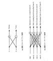
【0022】
データ点列数64の高速フーリエ変換を実行する場合を図5を用いて説明する。入力データA0…A63を図のように1段目の入力としてあたえる。1段目のバタフライ演算部10で基数4のバタフライ演算が行われデータB0…B63が出力される。これらのデータを2段目の入力に適するように、データの組を変更する必要がある。これを遅延量4のデータ並べ替え回路11で実行する。このデータ並べ替え回路11を経てデータは次段の入力に適したデータの組に変更される。
【0023】
並べ替えられたデータB0…B63は2段目のバタフライ演算部12に入力されて、基数4のバタフライ演算が実行され、データC0…C63が出力される。前段と同様に、これらのデータはデータ並べ替え回路13でデータの組が変更され、3段目のバタフライ演算部14に入力される。3段目のバタフライ演算回路で基数4のバタフライ演算が実行されて、データD0…D63が出力される。このデータD0…D63が高速フーリエ変換の結果となる。
【0024】
次に、この回路を用いてデータ点列数32の高速フーリエ変換を実行する場合を図6を用いて説明する。入力データA0…A31を図のように1段目の入力としてあたえ、1段目のバタフライ演算部15の基数を変更し、この演算部で基数2のバタフライ演算を行う。1段目のバタフライ演算部15の出力データB0…B31はデータ並べ替え回路16でデータの組の変更が行われ、次段に入力される。2段目以降は64点の変換と同様に基数4のバタフライ演算が実行され、得られた結果D0…D31が高速フーリエ変換の結果となる。
【0025】
同様にデータ点列数16の高速フーリエ変換を実行する場合は、図7に示すように入力データは1段目のバタフライ演算部17、データ並べ替え回路18をスキップする。これ以降の演算回路で基数4のバタフライ演算を行うことで得られるC0…C16が高速フーリエ変換の結果となっている。
【0026】
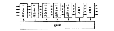
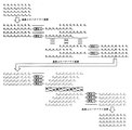
基数の変更や基本演算回路のスキップといった動作はデータ点列数Nをさらに増加させたときも同様の効果を示し、図8に示す回路では16〜16384点の高速フーリエ変換に対応することができる。
【0027】
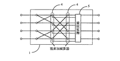
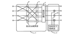
次に、基数の変更について図9、図10を用いて詳細に説明する。この場合、演算の切り替え方法は以下のとおりである。高速フーリエ変換の性質として、データ点列数の大きな高速フーリエ変換は、データ点列数のより小さな高速フーリエ変換を内部に含んでいる。この性質から、基数4のバタフライ演算には基数2のバタフライ演算が含まれていることがわかる。そこで、基数の切り替えが可能な演算回路では、基数4のバタフライ演算の途中で、基数2のバタフライ演算の結果を出力できるようにしておく。
【0028】
これは図9において、2段に接続された複素加減算器4の1段目の出力を取り出すことで実現される。この出力は2段目の複素加減算器4の入力と選択回路5の入力に接続される。2段目の複素加減算器4で演算された結果は基数4のバタフライ演算の結果となっているので、この基数4のバタフライ演算の結果と、基数2のバタフライ演算の結果を選択回路5で選択することで基数の変更を実現している。
【0029】
図9は基数が2のときのバタフライ演算部1、回転因子乗算部3の動作を示しており、実線で示した経路を通ってデータが流れていく。また、このときの回転因子は出力Bと出力Dにのみ乗算されるので、出力Cに乗算するための複素乗算器19は1を乗じるようにしておく。基数が4のときのバタフライ演算部1の動作は図10に示すようになり、図9と同様に実線部分をデータが流れていく。
【0030】
次に、基本演算回路のスキップについて説明する。この処理はある段の基本演算回路100の演算をまったく行わない。また、スキップされる基本演算回路100は常に前方の段であるので、基本演算回路100にスキップ用の特別な回路を付加することなく、スキップする段の次段に直接入力すればよいことになる。したがって、高速フーリエ変換演算回路の入力部で複数の段への入力を行えるようにしておき、この入力線を選択することでスキップ処理が容易に行えるようになる。
【0031】
これより、基本回路の内部には付加回路がないので、回路構成の縮小に役立てることができる。また、本発明においてはスキップする演算回路は常に前方のステージである。こうすることでスキップ処理を施した演算回路以降の演算において変更を加えることなく演算することができる。これは演算の流れ図を示した、図5〜7において最終の2段の演算の順番が同じであるということから容易に理解できる。この性質はデータ点列数が多くなっても同様である。
【0032】
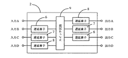
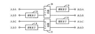
データ並べ替え回路2の変更方法について図11、図12を用いて詳細に説明する。データ並べ替え回路2はバタフライ演算部1の基数Rによって変更を加える必要がある。図3に示すのは基数4のときに用いられる構成である。データ並べ替え回路2では、まず、データ点列を入力A、入力B、入力C、入力Dからそれぞれシリアルに入力する。
【0033】
入力B、入力C、入力Dから入力されたそれぞれのデータは、高速フーリエ変換の各基本回路で必要とされるだけ遅延させる。このとき、入力Cに接続される遅延素子7の遅延量は入力Bに接続される遅延素子6の遅延量の2倍、入力Dに接続される遅延素子8の遅延量は遅延素子6の遅延量の3倍である。
【0034】
遅延させたデータは4個の入力を適切に配分するスイッチング回路9に入力する。スイッチング回路では図12に示すようにデータの交換を行う。データ交換を行った後、出力A、出力B、出力Cのデータを遅延させ、データ出力のタイミングをあわせ、出力する。このようにして各基本回路で必要となるデータの組になるように並べ替えを行う。また、基数2のバタフライ演算部1に対応する場合の回路のブロック図を図11に示す。
【0035】
基数2のバタフライ演算部1に対応したデータ並べ替え回路2の動作は以下のとおりである。データ点列は入力A、入力B、入力C、入力Dからそれぞれシリアルに入力され、入力B、入力Dから入力されたデータを高速フーリエ変換で必要な数だけ遅延させる。このとき、入力Bと入力Dに接続される遅延素子6,8の遅延量は等しくなる。
【0036】
この後、入力Aと入力B、入力Cと入力Dとでデータ交換をスイッチング回路20,21で、図12に示すように必要な部分で行う。データ交換を行った後、出力A、出力Cで入力で行った数の遅延を行い、出力のタイミングを調整し、出力する。
【0037】
本発明ではすべての基本演算回路の基数を変更可能にすることで、2個の高速フーリエ変換を同時に実行することが可能になる。この場合の回路のブロック図を図14に、データの流れ図を図15に示す。この演算では、すべての基本演算回路100で基数を2として演算する。また、この場合のデータ並べ替え回路2は上記に示した基数2のときの動作と同じ動作を示すが、遅延素子6,8における遅延量は上記の場合の平方根をとった数となる。
【0038】
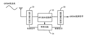
本発明の高速フーリエ変換回路をマルチキャリア直交周波数分割多重方式(OFDM)の受信機に用いた場合の構成を図16に示す。この場合、放送波の搬送波数Kは放送波からの信号により取り出すことができ、この情報は情報分離回路22で分離され、高速フーリエ変換回路の制御部24に送られる。この情報によりFFTの基本回路23に制御部24から制御信号が送られ、高速フーリエ変換回路の処理点数が変更される。このようにして、OFDMの搬送波数Kに対応した高速フーリエ変換点数N(N≧K)に瞬時に変更することが可能になる。
【0039】
上記実施形態においては、例として基数が4の場合の回路の構成方法について述べてきたが、これは基数Rを大きくしても同様の効果が得られ、ハードウェアの削減、高速化など新たな効果が期待できる。
【0040】
【発明の効果】
以上、説明したように、本発明の高速フーリエ変換演算回路は、処理するデータ点列数Nが基数Rに関係なくN/2、N/4、…と変更になっても同一の回路で高速フーリエ変換を行えるようにしたものである。この演算回路を用いることで、様々な点数の高速フーリエ変換にただ一つの回路で対応することができるようになったことが、本発明の最大の効果である。これにより、多様な入力数Nで高速フーリエ変換処理を必要とする場合に、単一のハードウェアで実現が可能となり、物量の削減等に効果を発揮できる。
【0041】
請求項1の発明では、様々な点数の高速フーリエ変換にただ1つの回路で対応することができる。請求項2の発明では、これまで複数個必要であったバタフライ演算回路を1個にすることができ、部品点数の削減に効果がある。請求項3の発明では、請求項2と同様にデータ並べ替え回路を1個にすることができ、部品点数の削減に効果がある。請求項4の発明では、後方の演算回路になんら影響を与えないので制御系統が簡略化される。請求項5の発明では、これまで同時に実行するには2個の演算回路が必要であったが、これを1個で行えることから、部品点数の削減、制御系統の簡略化の効果がある。
【図面の簡単な説明】
【図1】本発明の原理説明図である。
【図2】本発明の原理説明におけるバタフライ演算部のブロック図である。
【図3】本発明の原理説明におけるデータ並べ替え回路のブロック図である。
【図4】本発明の実施の形態の64点高速フーリエ変換回路のブロック図である。
【図5】本発明の実施の形態の64点高速フーリエ変換のデータの流れ図である。
【図6】本発明の実施の形態の32点高速フーリエ変換のデータの流れ図である。
【図7】本発明の実施の形態の16点高速フーリエ変換のデータの流れ図である。
【図8】本発明の実施の形態の16〜16384点に対応した高速フーリエ変換演算回路である。
【図9】本発明の実施の形態の基数が2の時の動作である。
【図10】本発明の実施の形態の基数が4の時の動作である。
【図11】本発明の実施の形態の基数が2の時のデータ並べ替え回路の動作ブロック図である。
【図12】本発明の実施の形態の32点高速フーリエ変換におけるデータ並べ替え回路の動作説明図である。
【図13】従来の高速フーリエ変換を説明する図である。
【図14】本発明の他の実施の形態のすべての基本演算回路を変更可能にしたときの演算回路である。
【図15】本発明の他の実施の形態の2個の高速フーリエ変換を同時に実行したときのデータの流れ図である。
【図16】本発明の他の実施の形態のOFDM受信機における本発明の利用である。
【符号の説明】
100 高速フーリエ変換基本回路
1,10,12,14,15,17 バタフライ演算部
2,11,13,16,18 データ並べ替え回路
3 回転因子乗算部
4 複素加減算器
5 選択回路
6,7,8 遅延素子
9,20,21 スイッチ回路
19 複素乗算器
22 制御信号分離部
23 FFT基本回路群
24 高速フーリエ変換回路の制御部[0001]
BACKGROUND OF THE INVENTION
The present invention relates to a fast Fourier transform used for signal processing, data analysis, linear systems, and the like. In particular, even if the number of input data points decreases with respect to the number of input data points N, fast Fourier transform (hereinafter referred to as FFT). The present invention relates to a fast Fourier transform arithmetic circuit capable of performing (abbreviated).
[0002]
[Prior art]
With the recent development of digital technology, preparations are being made to shift terrestrial television broadcasting from current analog broadcasting to digital broadcasting. In this terrestrial digital television broadcast, a multi-carrier orthogonal frequency division multiplexing modulation scheme (hereinafter abbreviated as OFDM) is expected to be adopted as a modulation scheme. In this OFDM, fast Fourier transform is used for modulation / demodulation of a carrier wave. The number of fast Fourier transform points N of the fast Fourier transform used in this modulation system depends on the number of OFDM carriers K.
[0003]
The number of carrier waves K varies from 1705 to 6817 on the standard, and these standards may further increase. In order to correspond to the number of the plurality of carrier waves, it is necessary to prepare a dedicated fast Fourier transform arithmetic circuit. Further, the existing fast Fourier transform arithmetic circuit capable of dealing with a plurality of data points is divided by a power of R such as N / R, N / R 2 , (R is a radix) for the number N. Only the score can be calculated.
[0004]
In addition, there are fast Fourier transform circuits corresponding to many points by providing butterfly operation circuits of different radixes. In this case, it is necessary to change the structure of all the rearrangement circuits, and control of the operation circuits Becomes difficult. Therefore, there is no circuit that can deal with various points in the same circuit regardless of R, and that can easily control the change of the data point sequence.
[0005]
[Problems to be solved by the invention]
As described above, in the conventional circuit for performing the fast Fourier transform, when the number N is determined, the circuit configuration is uniquely determined. Therefore, there has been a problem that even if the number of points of input data is changed and the number of input data is reduced, the same circuit cannot be operated.
[0006]
Further, even in a fast Fourier transform arithmetic circuit capable of changing the score, the score can be changed only by a power of 1 of the radix R. That is, there is a problem that the change of the score depends on the radix R.
[0007]
An object of the present invention is to provide a circuit in which conversion points are set regardless of the radix R and conversion can be performed by the same circuit even if the number of input data points is reduced in view of the above-described conventional drawbacks. Is.
[0008]
[Means for Solving the Problems]
FIG. 1 is a diagram for explaining the principle of the present invention. FIG. 1 (a) shows the concept of data input to the basic circuit, and FIG. 1 (b) shows a configuration example of the basic circuit of the present invention. FIG. 2 shows a configuration example of the butterfly operation circuit according to the present invention, and FIG. 3 shows a configuration example of the data rearrangement circuit. The above problems are solved by a fast Fourier transform circuit configured as follows.
[0009]
(1) A circuit for performing a fast Fourier transform on a fast Fourier transform (FFT) number N to be processed, and an R-input basic
[0010]
(2) The fast Fourier transform operation circuit shown in (1), which includes a signal line that outputs the progress of the butterfly operation, and allows the selection circuit 5 to select the signal line signal and other calculation results. A radix can be changed by an external signal.
[0011]
(3) The fast Fourier transform circuit shown in (1), which is a data rearrangement circuit in the basic
[0012]
(4) The fast Fourier transform operation circuit shown in (1), in which the M-stage
[0013]
(5) The fast Fourier transform arithmetic circuit shown in (1), wherein all the basic
[0015]
In the configuration described above, a basic
[0016]
At this time, by changing the radix of one or a plurality of
[0017]
According to the present invention, it is possible to perform a fast Fourier transform corresponding to a plurality of data point sequences without a significant increase in hardware. Also, according to the configuration of the present invention, two independent data can be Fourier transformed at high speed.
[0018]
DETAILED DESCRIPTION OF THE INVENTION
Hereinafter, embodiments of the present invention will be described in detail with reference to the drawings. 1 to 3 are diagrams for explaining the principle of the present invention, and FIGS. 4 to 12 are diagrams showing an embodiment of the present invention. FIG. 13 is a diagram for explaining a conventional fast Fourier transform, and FIGS. 14 to 16 show another embodiment of the present invention.
[0019]
In the present invention, the Fast Fourier Transform (FFT) N-point Fast Fourier Transform arithmetic circuit comprises M (= log R N) basic
[0020]
When the number N of input data decreases in such a fast Fourier transform arithmetic circuit, the change in the number of input data is accommodated by changing the radix R in the butterfly arithmetic circuit. As an example of the calculation in this case, the radix R is 4, and the number of fast Fourier transform points N = 64.
[0021]
Because it is 64 = 4 3,
[0022]
A case where the fast Fourier transform of 64 data point sequences is executed will be described with reference to FIG. Input data A 0 ... A 63 is given as the first stage input as shown in the figure. The
[0023]
Data B 0 ... B 63 rearranged is input to the
[0024]
Next, the case where the fast Fourier transform of 32 data point sequences is executed using this circuit will be described with reference to FIG. Input data A 0 ... A 31 is input as the first stage as shown in the figure, and the radix of the first stage
[0025]
Similarly, when the fast Fourier transform with 16 data point sequences is executed, the input data skips the first stage
[0026]
Operations such as changing the radix and skipping the basic arithmetic circuit show the same effect when the number N of data point sequences is further increased, and the circuit shown in FIG. 8 can cope with the fast Fourier transform of 16 to 16384 points. .
[0027]
Next, the change of the radix will be described in detail with reference to FIGS. In this case, the calculation switching method is as follows. As a property of the fast Fourier transform, the fast Fourier transform having a large number of data point sequences includes a fast Fourier transform having a smaller number of data point sequences. From this property, it can be seen that the radix-4 butterfly operation includes the radix-2 butterfly operation. Therefore, an arithmetic circuit capable of switching the radix is configured so that the result of the radix-2 butterfly computation can be output during the radix-4 butterfly computation.
[0028]
This is realized by taking out the output of the first stage of the complex adder /
[0029]
FIG. 9 shows the operation of the
[0030]
Next, skipping of the basic arithmetic circuit will be described. This processing does not perform any operation of the basic
[0031]
As a result, there is no additional circuit inside the basic circuit, which can be used for reducing the circuit configuration. In the present invention, the skipped arithmetic circuit is always the front stage. By doing so, it is possible to perform an operation without any change in the operation after the operation circuit subjected to the skip processing. This can be easily understood from the fact that the order of the final two stages of operations in FIGS. This property is the same even when the number of data point sequences increases.
[0032]
A method for changing the
[0033]
The data inputted from the input B, the input C, and the input D are delayed as required in each basic circuit of the fast Fourier transform. At this time, the delay amount of the
[0034]
The delayed data is input to the switching circuit 9 that appropriately distributes the four inputs. The switching circuit exchanges data as shown in FIG. After data exchange, the data of output A, output B, and output C are delayed, and the data output timing is matched and output. In this way, rearrangement is performed so as to obtain a data set necessary for each basic circuit. FIG. 11 is a block diagram of a circuit corresponding to the radix-2
[0035]
The operation of the
[0036]
Thereafter, data exchange between the input A and the input B, and the input C and the input D is performed by the switching
[0037]
In the present invention, by making it possible to change the radix of all the basic arithmetic circuits, two Fast Fourier Transforms can be executed simultaneously. A block diagram of the circuit in this case is shown in FIG. 14, and a data flow diagram is shown in FIG. In this calculation, all the basic
[0038]
FIG. 16 shows a configuration when the fast Fourier transform circuit of the present invention is used in a multicarrier orthogonal frequency division multiplexing (OFDM) receiver. In this case, the number of carrier waves K of the broadcast wave can be extracted by a signal from the broadcast wave, and this information is separated by the
[0039]
In the above embodiment, the circuit configuration method in the case where the radix is 4 has been described as an example. However, the same effect can be obtained even if the radix R is increased. The effect can be expected.
[0040]
【The invention's effect】
As described above, the fast Fourier transform arithmetic circuit according to the present invention is high speed with the same circuit even if the number N of data point sequences to be processed is changed to N / 2, N / 4,. The Fourier transform can be performed. By using this arithmetic circuit, it is possible to cope with various points of fast Fourier transform with only one circuit, which is the greatest effect of the present invention. As a result, when fast Fourier transform processing is required with various numbers of inputs N, it can be realized with a single piece of hardware, which can be effective in reducing physical quantities.
[0041]
According to the first aspect of the present invention, it is possible to cope with various points of the fast Fourier transform with a single circuit. According to the second aspect of the present invention, the number of butterfly operation circuits that have been required in the past can be reduced to one, which is effective in reducing the number of parts. In the invention of
[Brief description of the drawings]
FIG. 1 is a diagram illustrating the principle of the present invention.
FIG. 2 is a block diagram of a butterfly operation unit in the explanation of the principle of the present invention.
FIG. 3 is a block diagram of a data rearrangement circuit in the principle explanation of the present invention.
FIG. 4 is a block diagram of a 64-point fast Fourier transform circuit according to the embodiment of the present invention.
FIG. 5 is a data flow diagram of 64-point fast Fourier transform according to the embodiment of the present invention.
FIG. 6 is a data flow diagram of 32-point fast Fourier transform according to the embodiment of the present invention.
FIG. 7 is a data flow diagram of 16-point fast Fourier transform according to the embodiment of the present invention.
FIG. 8 is a fast Fourier transform arithmetic circuit corresponding to 16 to 16384 points according to the embodiment of the present invention.
FIG. 9 shows the operation when the radix is 2 in the embodiment of the present invention.
FIG. 10 shows the operation when the radix is 4 according to the embodiment of this invention.
FIG. 11 is an operation block diagram of the data rearrangement circuit when the radix is 2 according to the embodiment of this invention.
FIG. 12 is an operation explanatory diagram of the data rearrangement circuit in the 32-point fast Fourier transform according to the embodiment of the present invention.
FIG. 13 is a diagram for explaining a conventional fast Fourier transform.
FIG. 14 is an arithmetic circuit when all the basic arithmetic circuits according to another embodiment of the present invention are changeable.
FIG. 15 is a data flow diagram when two fast Fourier transforms are simultaneously executed according to another embodiment of the present invention.
FIG. 16 is an application of the present invention in an OFDM receiver of another embodiment of the present invention.
[Explanation of symbols]
100 Fast Fourier
Claims (5)
バタフライ演算部1、回転因子乗算部3、データ並べ替え回路2からなるR入力の基本演算回路100を1段として、これをM個(=logRN)(Rは基数)直列に並べて高速フーリエ変換が行えるように構成し、
前記バタフライ演算部1では、上記R入力間で基数Rのたすき掛け演算を行い、
前記回転因子乗算部3では、バタフライ演算部2の出力のうちR−1個の出力に対して回転因子の乗算を行い、
前記データ並べ替え回路2では、上記入力データNに対し2段目以降の演算に必要となるデータの組を生成し、
さらに、外部からの制御信号により、前記バタフライ演算部1の基数が変更可能であり、
前記回転因子乗算部3、および前記データ並べ替え回路2を基数に応じて変更できる基本演算回路100を1個もしくは複数個備え、そのうち、1個もしくは複数個の基本演算回路100の基数を変更することで、上記高速フーリエ変換点数Nが基数Rに関わりなくN/2、N/4、…となっても同一の回路で高速フーリエ変換を行うことを特徴とする高速フーリエ変換演算回路。A circuit that performs fast Fourier transform on the number N of fast Fourier transform points to be processed,
The R input basic arithmetic circuit 100 including the butterfly arithmetic unit 1, the twiddle factor multiplying unit 3, and the data rearrangement circuit 2 is arranged in one stage, and M (= log RN) (R is a radix) are arranged in series to perform fast Fourier transform. Configured to do so,
The butterfly calculation unit 1 performs a radix R multiplication operation between the R inputs,
The twiddle factor multiplication unit 3 multiplies R-1 outputs among the outputs of the butterfly computation unit 2 by multiplication of the twiddle factor.
The data rearrangement circuit 2 generates a set of data necessary for the second and subsequent calculations for the input data N,
Furthermore, the radix of the butterfly computing unit 1 can be changed by an external control signal,
The twiddle factor multiplication unit 3 and the data rearrangement circuit 2 are provided with one or a plurality of basic arithmetic circuits 100 that can be changed according to the radix, and the radix of one or a plurality of basic arithmetic circuits 100 is changed. Therefore, even if the fast Fourier transform point N becomes N / 2, N / 4,... Regardless of the radix R, the fast Fourier transform operation circuit performs the fast Fourier transform in the same circuit.
バタフライ演算の途中経過を出力する信号線を備え、選択回路5により、前記信号線の信号とほかの計算結果が選択できるバタフライ演算部1を備え、外部からの信号により、基数の変更を可能にしたことを特徴とする高速フーリエ変換演算回路。In the fast Fourier transform arithmetic circuit according to claim 1,
A signal line that outputs the progress of butterfly computation is provided, and a butterfly computation unit 1 that can select a signal of the signal line and other calculation results by a selection circuit 5 is provided. The radix can be changed by an external signal. A fast Fourier transform operation circuit characterized by the above.
基本演算回路100におけるデータ並べ替え回路で、入力段に複数の遅延量が可変な遅延素子6,7,8を備え、基数に応じて切り替え状態を変更できるスイッチ回路9を備え、出力段に複数の遅延量が可変の遅延素子6,7,8を備え、外部からの制御信号に基づいて基数が変更に対応することが可能なデータ並べ替え回路を持つことを特徴とする高速フーリエ変換演算回路。In the fast Fourier transform arithmetic circuit according to claim 1,
The data rearrangement circuit in the basic arithmetic circuit 100 includes a plurality of delay elements 6, 7, and 8 with variable delay amounts at the input stage, a switch circuit 9 that can change the switching state according to the radix, and a plurality of output stages. A fast Fourier transform arithmetic circuit comprising delay elements 6, 7, and 8 having variable delay amounts, and a data rearrangement circuit capable of responding to a change in radix based on an external control signal .
M段の基本演算回路100を直列に接続した回路は、前方からL段(L≦M)を基数が変更可能な基本演算回路であることを特徴とする高速フーリエ変換演算回路。In the fast Fourier transform arithmetic circuit according to claim 1,
A fast Fourier transform arithmetic circuit characterized in that a circuit in which M-stage basic arithmetic circuits 100 are connected in series is a basic arithmetic circuit whose radix can be changed from the L stage (L ≦ M) from the front.
全ての基本演算回路100を基数が変更可能な演算回路とし、すべての基本演算回路100で基数をRより小さく、同一の値に設定し、前記データ並べ替え回路2は、遅延量を変更できる遅延素子6,8の遅延量を等しくし、外部からの制御信号に基づいてそれぞれ独立した入力データをフーリエ変換し出力することが可能であることを特徴とする高速フーリエ変換演算回路。In the fast Fourier transform arithmetic circuit according to claim 1,
All the basic arithmetic circuits 100 are arithmetic circuits whose radix can be changed. In all the basic arithmetic circuits 100, the radix is set smaller than R and set to the same value, and the data rearrangement circuit 2 is a delay whose delay amount can be changed. A fast Fourier transform arithmetic circuit characterized in that the delay amounts of the elements 6 and 8 are equalized and independent input data can be subjected to Fourier transform and output based on an external control signal.
Priority Applications (1)
| Application Number | Priority Date | Filing Date | Title |
|---|---|---|---|
| JP08799997A JP3668356B2 (en) | 1997-04-07 | 1997-04-07 | Fast Fourier transform circuit |
Applications Claiming Priority (1)
| Application Number | Priority Date | Filing Date | Title |
|---|---|---|---|
| JP08799997A JP3668356B2 (en) | 1997-04-07 | 1997-04-07 | Fast Fourier transform circuit |
Publications (2)
| Publication Number | Publication Date |
|---|---|
| JPH10283341A JPH10283341A (en) | 1998-10-23 |
| JP3668356B2 true JP3668356B2 (en) | 2005-07-06 |
Family
ID=13930494
Family Applications (1)
| Application Number | Title | Priority Date | Filing Date |
|---|---|---|---|
| JP08799997A Expired - Lifetime JP3668356B2 (en) | 1997-04-07 | 1997-04-07 | Fast Fourier transform circuit |
Country Status (1)
| Country | Link |
|---|---|
| JP (1) | JP3668356B2 (en) |
Families Citing this family (11)
| Publication number | Priority date | Publication date | Assignee | Title |
|---|---|---|---|---|
| KR100628303B1 (en) * | 2004-09-03 | 2006-09-27 | 한국전자통신연구원 | Variable point IFT / FTF method and apparatus |
| US8229014B2 (en) | 2005-03-11 | 2012-07-24 | Qualcomm Incorporated | Fast fourier transform processing in an OFDM system |
| US8266196B2 (en) | 2005-03-11 | 2012-09-11 | Qualcomm Incorporated | Fast Fourier transform twiddle multiplication |
| JP4698394B2 (en) | 2005-11-25 | 2011-06-08 | パナソニック株式会社 | Fast Fourier transform circuit |
| KR101045713B1 (en) * | 2006-04-28 | 2011-06-30 | 콸콤 인코포레이티드 | Multi-Port Mixed Radix FFT |
| JP5601327B2 (en) * | 2009-09-24 | 2014-10-08 | 日本電気株式会社 | Data rearrangement circuit, variable delay circuit, fast Fourier transform circuit, and data rearrangement method |
| JP5556323B2 (en) * | 2010-04-15 | 2014-07-23 | 日本電気株式会社 | Control information automatic generation method for data rearrangement circuit, data rearrangement circuit, computer, and control information automatic generation program |
| EP2940594A4 (en) * | 2012-12-25 | 2016-09-21 | Nec Corp | CALCULATION DEVICE AND CALCULATION METHOD |
| WO2014104520A1 (en) * | 2012-12-27 | 2014-07-03 | 전자부품연구원 | Transform method, computation method and hevc system to which same are applied |
| US20200372095A1 (en) | 2017-08-07 | 2020-11-26 | Nec Corporation | Fast fourier transform device, data sorting processing device, fast fourier transform processing method, and program recording medium |
| JP7086321B2 (en) * | 2020-04-14 | 2022-06-17 | 三菱電機株式会社 | Frequency analyzer, frequency analysis method, control circuit and storage medium |
-
1997
- 1997-04-07 JP JP08799997A patent/JP3668356B2/en not_active Expired - Lifetime
Also Published As
| Publication number | Publication date |
|---|---|
| JPH10283341A (en) | 1998-10-23 |
Similar Documents
| Publication | Publication Date | Title |
|---|---|---|
| KR100551111B1 (en) | Pipeline Fast Fourier Transform Processor | |
| US5717620A (en) | Improved-accuracy fast-Fourier-transform butterfly circuit | |
| JP3668356B2 (en) | Fast Fourier transform circuit | |
| US20050047325A1 (en) | Combined inverse fast fourier transform and guard interval processing for efficient implementation of OFDM based systems | |
| WO2007115329A2 (en) | Pipeline fft architecture and method | |
| WO1979000271A1 (en) | Fdm/tdm transmultiplexer | |
| US4646256A (en) | Computer and method for the discrete bracewell transform | |
| US5270953A (en) | Fast convolution multiplier | |
| EP0944005A1 (en) | Arithmetic unit and method for fourier transform | |
| US3777131A (en) | High base multiple rail fourier transform serial stage | |
| KR20090127462A (en) | FTF / IFFT Core | |
| JPH06243161A (en) | Discreteness cosine converting circuit | |
| US6157938A (en) | Fast fourier transform device with parallel lattice architecture | |
| US8010588B2 (en) | Optimized multi-mode DFT implementation | |
| JPH08320858A (en) | Fourier transform computing device and method | |
| KR100602272B1 (en) | Fast Fourier Transform Device and Method for Processing Data at High Speed | |
| JPH10307811A (en) | Arithmetic unit and arithmetic method | |
| KR101334494B1 (en) | High-speed low-complexity radix-2 to the fifth fast fourier transform apparatus and method | |
| KR100576520B1 (en) | Variable Fast Fourier Transform Processor Using Iterative Arithmetic | |
| KR20120109214A (en) | Fft processor and fft method for ofdm system | |
| KR101711783B1 (en) | Apparatus and method for high-speed low-complexity mixed-radix fast fourier transform using dual-path sharing method | |
| JP3865469B2 (en) | Butterfly calculator | |
| Ho et al. | A reconfigurable systolic array architecture for multicarrier wireless and multirate applications | |
| KR20090043210A (en) | FFT / IFFT dual mode device and control method thereof for OPDM | |
| CN121255285A (en) | Dynamic configurable pipeline FFT processor supporting multiple points and implementation method thereof |
Legal Events
| Date | Code | Title | Description |
|---|---|---|---|
| A131 | Notification of reasons for refusal |
Free format text: JAPANESE INTERMEDIATE CODE: A131 Effective date: 20040210 |
|
| A02 | Decision of refusal |
Free format text: JAPANESE INTERMEDIATE CODE: A02 Effective date: 20050208 |
|
| A521 | Written amendment |
Free format text: JAPANESE INTERMEDIATE CODE: A523 Effective date: 20050303 |
|
| A911 | Transfer of reconsideration by examiner before appeal (zenchi) |
Free format text: JAPANESE INTERMEDIATE CODE: A911 Effective date: 20050308 |
|
| TRDD | Decision of grant or rejection written | ||
| A01 | Written decision to grant a patent or to grant a registration (utility model) |
Free format text: JAPANESE INTERMEDIATE CODE: A01 Effective date: 20050329 |
|
| A61 | First payment of annual fees (during grant procedure) |
Free format text: JAPANESE INTERMEDIATE CODE: A61 Effective date: 20050408 |
|
| R150 | Certificate of patent or registration of utility model |
Free format text: JAPANESE INTERMEDIATE CODE: R150 |
|
| S111 | Request for change of ownership or part of ownership |
Free format text: JAPANESE INTERMEDIATE CODE: R313114 |
|
| FPAY | Renewal fee payment (event date is renewal date of database) |
Free format text: PAYMENT UNTIL: 20080415 Year of fee payment: 3 |
|
| R350 | Written notification of registration of transfer |
Free format text: JAPANESE INTERMEDIATE CODE: R350 |
|
| FPAY | Renewal fee payment (event date is renewal date of database) |
Free format text: PAYMENT UNTIL: 20080415 Year of fee payment: 3 |
|
| FPAY | Renewal fee payment (event date is renewal date of database) |
Free format text: PAYMENT UNTIL: 20090415 Year of fee payment: 4 |
|
| FPAY | Renewal fee payment (event date is renewal date of database) |
Free format text: PAYMENT UNTIL: 20090415 Year of fee payment: 4 |
|
| FPAY | Renewal fee payment (event date is renewal date of database) |
Free format text: PAYMENT UNTIL: 20100415 Year of fee payment: 5 |
|
| FPAY | Renewal fee payment (event date is renewal date of database) |
Free format text: PAYMENT UNTIL: 20100415 Year of fee payment: 5 |
|
| FPAY | Renewal fee payment (event date is renewal date of database) |
Free format text: PAYMENT UNTIL: 20110415 Year of fee payment: 6 |
|
| FPAY | Renewal fee payment (event date is renewal date of database) |
Free format text: PAYMENT UNTIL: 20110415 Year of fee payment: 6 |
|
| FPAY | Renewal fee payment (event date is renewal date of database) |
Free format text: PAYMENT UNTIL: 20120415 Year of fee payment: 7 |
|
| FPAY | Renewal fee payment (event date is renewal date of database) |
Free format text: PAYMENT UNTIL: 20130415 Year of fee payment: 8 |
|
| FPAY | Renewal fee payment (event date is renewal date of database) |
Free format text: PAYMENT UNTIL: 20140415 Year of fee payment: 9 |
|
| R250 | Receipt of annual fees |
Free format text: JAPANESE INTERMEDIATE CODE: R250 |
|
| EXPY | Cancellation because of completion of term |