JP4698394B2 - Fast Fourier transform circuit - Google Patents
Fast Fourier transform circuit Download PDFInfo
- Publication number
- JP4698394B2 JP4698394B2 JP2005340148A JP2005340148A JP4698394B2 JP 4698394 B2 JP4698394 B2 JP 4698394B2 JP 2005340148 A JP2005340148 A JP 2005340148A JP 2005340148 A JP2005340148 A JP 2005340148A JP 4698394 B2 JP4698394 B2 JP 4698394B2
- Authority
- JP
- Japan
- Prior art keywords
- butterfly
- fourier transform
- fast fourier
- buffer
- digital signal
- Prior art date
- Legal status (The legal status is an assumption and is not a legal conclusion. Google has not performed a legal analysis and makes no representation as to the accuracy of the status listed.)
- Expired - Fee Related
Links
Images


Classifications
-
- G—PHYSICS
- G06—COMPUTING; CALCULATING OR COUNTING
- G06F—ELECTRIC DIGITAL DATA PROCESSING
- G06F17/00—Digital computing or data processing equipment or methods, specially adapted for specific functions
- G06F17/10—Complex mathematical operations
- G06F17/14—Fourier, Walsh or analogous domain transformations, e.g. Laplace, Hilbert, Karhunen-Loeve, transforms
- G06F17/141—Discrete Fourier transforms
- G06F17/142—Fast Fourier transforms, e.g. using a Cooley-Tukey type algorithm
-
- H—ELECTRICITY
- H04—ELECTRIC COMMUNICATION TECHNIQUE
- H04L—TRANSMISSION OF DIGITAL INFORMATION, e.g. TELEGRAPHIC COMMUNICATION
- H04L27/00—Modulated-carrier systems
- H04L27/26—Systems using multi-frequency codes
- H04L27/2601—Multicarrier modulation systems
- H04L27/2647—Arrangements specific to the receiver only
- H04L27/2649—Demodulators
- H04L27/265—Fourier transform demodulators, e.g. fast Fourier transform [FFT] or discrete Fourier transform [DFT] demodulators
- H04L27/26522—Fourier transform demodulators, e.g. fast Fourier transform [FFT] or discrete Fourier transform [DFT] demodulators using partial FFTs
Description
本発明は、高速フーリエ変換回路に関する。 The present invention relates to a fast Fourier transform circuit.
従来、複数の通信方式に対応可能な高速フーリエ変換回路(以下「マルチモード高速フーリエ変換回路」という)としては、例えば、特許文献1に記載されているものがある。
Conventionally, as a fast Fourier transform circuit (hereinafter referred to as “multi-mode fast Fourier transform circuit”) capable of supporting a plurality of communication methods, there is one described in
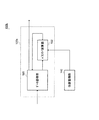
図11は、特許文献1に記載された従来のマルチモード高速フーリエ変換回路の構成を示すブロック図である。
FIG. 11 is a block diagram showing a configuration of a conventional multimode fast Fourier transform circuit described in
図11に示すマルチモード高速フーリエ変換回路1は、直列並列変換回路11、直列並列変換回路12、スイッチ13、FFT(Fast Fourier Transform:高速フーリエ変換)回路14、並列直列変換回路15、間引き回路16、振幅調整回路17、ゼロ信号生成回路18、直列並列変換回路19、および合成器20を有する。
A multimode fast Fourier
この回路1においては、P(=2048)ポイントのFFT処理を必要とするOFDM(Orthogonal Frequency Division Multiplexing:直交周波数分割多重)方式と、Q(=64)ポイントのFFT処理を必要とするOFDM方式とに対応する場合、いずれもPポイントのFFT処理を行う。ここで、QポイントのFFT処理を必要とするOFDM方式の信号を受信する場合には、合成器20において受信信号とゼロ信号生成回路18から出力されるゼロ値のデータとを合成することにより、Q本のパラレルデータをP本のパラレルデータに変換することによって、PポイントのFFT処理を行う。
In this
しかしながら、上記した従来のマルチモード高速フーリエ変換回路においては、Q(<P)ポイントのFFT処理を必要とするOFDM方式の信号を受信する場合にもPポイントのFFT処理を行うため、余分な演算を行うことになり、演算リソースの最適化が図れていないという問題がある。 However, in the conventional multi-mode fast Fourier transform circuit described above, the P point FFT process is performed even when receiving an OFDM signal that requires an FFT process of Q (<P) points. There is a problem that optimization of computing resources cannot be achieved.
なお、近年は、テレビの受信機能を有する通信装置の需要が高まっており、通信中でもテレビを受信できるよう、任意の複数の通信方式(OFDM方式に限定されない)に対して、同時にFFT処理を行うことができるマルチモード高速フーリエ変換回路が求められている。このようなマルチモード高速フーリエ変換回路において、複数のFFT処理を効率化するべく、演算リソースの最適化を図ることは、回路の小型化と省電力化につながり、極めて有益である。 In recent years, demand for communication devices having a television reception function has increased, and FFT processing is simultaneously performed on any of a plurality of communication methods (not limited to the OFDM method) so that television can be received even during communication. There is a need for a multi-mode fast Fourier transform circuit that can do this. In such a multi-mode fast Fourier transform circuit, optimizing the computation resources in order to improve the efficiency of a plurality of FFT processes leads to miniaturization of the circuit and power saving, which is extremely beneficial.
本発明は、かかる点に鑑みてなされたものであり、複数の通信方式に対応しつつ、演算リソースの最適化を図ることができる高速フーリエ変換回路を提供することを目的とする。 The present invention has been made in view of this point, and an object of the present invention is to provide a fast Fourier transform circuit capable of optimizing calculation resources while supporting a plurality of communication methods.
本発明の高速フーリエ変換回路は、2N(Nは自然数)個のデジタル信号を蓄積し、各ビットの並び順を逆転させたビットリバーサルの位置に並び替えたデジタル信号を出力する第1のバッファと、2M(Mは自然数、但し、M≦N)個のデジタル信号を蓄積し、ビットリバーサルの位置に並び替えたデジタル信号を出力する第2のバッファと、前記第1のバッファから出力されたデジタル信号に対する第1のバタフライ演算処理と、前記第2のバッファから出力されたデジタル信号に対する第2のバタフライ演算処理とを行う第1の高速フーリエ変換処理部と、前記第1のバタフライ演算処理後のデジタル信号に対して、バタフライ演算処理を行う第2の高速フーリエ変換処理部と、前記第2のバタフライ演算処理後のデジタル信号に対して、バタフライ演算処理を行う第3の高速フーリエ変換処理部と、を有する構成を採る。 The fast Fourier transform circuit of the present invention accumulates 2 N (N is a natural number) digital signals, and outputs a digital signal rearranged at a bit reversal position in which the order of each bit is reversed. And 2 M (M is a natural number, where M ≦ N) digital signals are accumulated and output from the first buffer, and the second buffer outputs the digital signal rearranged at the bit reversal position. a first butterfly computation process and the second first fast Fourier transform unit for performing a second butterfly computation processing against the digital signal output from the buffer against the digital signal, the first respect of the digital signal after the butterfly computation process, the second fast Fourier transform unit for performing bus Tafurai processing, pair into digital signals after the second butterfly computation process To adopts a configuration having a third fast Fourier transform unit for performing bus Tafurai processing, the.
また、本発明の高速フーリエ変換回路は、2N(Nは自然数)個のデジタル信号を蓄積し、各ビットの並び順を逆転させたビットリバーサルの位置に並び替えたデジタル信号を出力する第1のバッファと、2M(Mは自然数、但し、M≦N)個のデジタル信号を蓄積し、ビットリバーサルの位置に並び替えたデジタル信号を出力する第2のバッファと、前記第1のバッファから出力されたデジタル信号に対する第1のバタフライ演算処理と、前記第2のバッファから出力されたデジタル信号に対する第2のバタフライ演算処理とを行う第1の高速フーリエ変換処理部と、前記第1のバタフライ演算処理後のデジタル信号に対する第3のバタフライ演算処理と、前記第2のバタフライ演算処理後のデジタル信号に対する第4のバタフライ演算処理とを行う第2の高速フーリエ変換処理部と、前記第3のバタフライ演算処理後のデジタル信号に対して、バタフライ演算処理を行う第3の高速フーリエ変換処理部と、を有する構成を採る。 The fast Fourier transform circuit of the present invention accumulates 2 N (N is a natural number) digital signals, and outputs a digital signal rearranged at a bit reversal position in which the order of each bit is reversed. A second buffer that stores 2 M (M is a natural number, where M ≦ N) digital signals and outputs a digital signal rearranged at the bit reversal position, and the first buffer. a first butterfly computation processing against output digital signal, said first fast Fourier transform unit for performing a second butterfly computation processing against output digital signals from the second buffer, the a third butterfly computation processing against the first digital signal after the butterfly computation process, the fourth butterfly operation against a digital signal after the second butterfly computation process Taking a second Fast Fourier transform processor for performing a processing with respect to the third digital signal after butterfly computation process, the third fast Fourier transform unit for performing bus Tafurai processing, a configuration having a .
また、本発明の高速フーリエ変換回路は、2N(Nは自然数)個のデジタル信号を蓄積し、各ビットの並び順を逆転させたビットリバーサルの位置に並び替えたデジタル信号を出力する第1のバッファと、2N−1個のデジタル信号を蓄積し、ビットリバーサルの位置に並び替えたデジタル信号を出力する第2のバッファと、前記第1のバッファの後段側に接続され、デジタル信号を蓄積するN個のデータ蓄積部と、前記第2のバッファの後段側に接続され、デジタル信号を蓄積する(N−1)個のデータ蓄積部と、前記N個のデータ蓄積部に蓄積されたデジタル信号に対する1段目からN段目のバタフライ演算処理と、前記(N−1)個のデータ蓄積部に蓄積されたデジタル信号に対する1段目から(N−1)段目のバタフライ演算処理とを行うN個のバタフライ演算部と、前記第1のバッファまたは前記第2のバッファならびに前記N個のバタフライ演算部から入力したデジタル信号の出力先を切り替えるN個のスイッチと、を有し、前記N個のスイッチは、それぞれ、入力したデジタル信号を設定に応じて次段のデータ蓄積部または次段のスイッチに出力する、構成を採る。 The fast Fourier transform circuit of the present invention accumulates 2 N (N is a natural number) digital signals, and outputs a digital signal rearranged at a bit reversal position in which the order of each bit is reversed. and buffers, 2 accumulates the N-1 digital signals, a second buffer which outputs a digital signal rearranged to the position of the bit reversal is connected in the subsequent stage of the first buffer, digital signal and N data storage unit for storing, which is connected to the second-stage side of the second buffer stores the digital signal and (N-1) data storage unit, stored in the N data storage unit a butterfly computation process of the N-th stage from the first stage to pair the digital signal, the (N-1) pieces from the first stage against the accumulated digital signal in the data storage unit (N-1) stage Eye butterfly computation N butterfly operation units for performing the operation, and N switches for switching output destinations of digital signals input from the first buffer or the second buffer and the N butterfly operation units, Each of the N switches employs a configuration in which the input digital signal is output to the next-stage data storage unit or the next-stage switch according to the setting.
本発明によれば、複数の通信方式に対応しつつ、演算リソースの最適化を図ることができる。 According to the present invention, it is possible to optimize computation resources while supporting a plurality of communication methods.
以下、本発明の実施の形態について、図面を参照して詳細に説明する。 Hereinafter, embodiments of the present invention will be described in detail with reference to the drawings.
(実施の形態1)
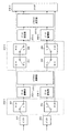
図1は、本発明の実施の形態1に係る高速フーリエ変換回路の構成を示すブロック図である。
(Embodiment 1)
FIG. 1 is a block diagram showing a configuration of a fast Fourier transform circuit according to
図1に示す高速フーリエ変換回路(以下「FFT回路」という)100は、複数の通信方式に対応可能なマルチモード高速フーリエ変換回路である。ここでは、2Nポイント(Nは自然数)のFFT処理を必要とする通信方式と、2Mポイント(Mは自然数、但し、M≦Nとする)のFFT処理を必要とする通信方式とを同時処理する場合について説明する。2NポイントのFFT処理を行う場合は、基数2のバタフライ演算処理をN段行う必要があり、2MポイントのFFT処理を行う場合は、基数2のバタフライ演算処理をM段行う必要がある。 A fast Fourier transform circuit (hereinafter referred to as “FFT circuit”) 100 shown in FIG. 1 is a multimode fast Fourier transform circuit that can support a plurality of communication methods. Here, a communication method requiring 2 N points (N is a natural number) FFT processing and a communication method requiring 2 M points (M is a natural number, where M ≦ N) FFT processing are simultaneously performed. A case of processing will be described. When performing 2 N- point FFT processing, it is necessary to perform radix-2 butterfly computation processing in N stages. When performing 2 M- point FFT processing, it is necessary to perform radix-2 butterfly computation processing in M stages.
図1に示すFFT回路100は、第1のFFT処理部110、第2のFFT処理部120、第3のFFT処理部130、係数蓄積部140、および制御部150を有する。
1 includes a first
第1のFFT処理部110は、第1のバッファ111と、第1−1から第1−(M−1)までの(M−1)個のデータ蓄積部112−1〜112−(M−1)と、第2のバッファ113と、第2−1から第2−(M−1)までの(M−1)個のデータ蓄積部114−1〜114−(M−1)と、第1から第(M−1)までの(M−1)個のバタフライ演算部115−1〜115−(M−1)とを有し、第1のバッファ111および第2のバッファ113に入力されたデジタル信号に対して、(M−1)段(つまり、1段目から(M−1)段目まで)のFFT処理を行う。
The first
第2のFFT処理部120は、第1−Mから第1−Nまでの(N−M+1)個のデータ蓄積部121―M〜121―Nと、第Mから第Nまでの(N−M+1)個のバタフライ演算部122−M〜122−Nとを有し、第1のバッファ111に入力され第1のFFT処理部110でFFT処理されたデジタル信号に対して、(N−M+1)段(つまり、M段目からN段目まで)のFFT処理を行う。
The second
第3のFFT処理部130は、第2−Mのデータ蓄積部131と、第2−Mのバタフライ演算部132とを有し、第2のバッファ113に入力され第1のFFT処理部110でFFT処理されたデジタル信号に対して、1段(つまり、M段目)のFFT処理を行う。
The third
第1のバッファ111は、2N個のデジタル信号を蓄積し、制御部150の制御により、蓄積されたデジタル信号を第1−1のデータ蓄積部112−1に出力する。このとき、第1のバッファ111に入力されたデジタル信号は、各ビットの並び順を逆転させたビットリバーサルの位置に並び替えられて出力される。例えば、図2に示すように、入力されたデジタル信号は、0、1、…、2N−2、2N−1という並びを、ビットリバーサルの位置に並び替えた0、2N−1、…、2N−1−1、2N−1という並びに変換して出力される。
The
第2のバッファ113は、2M個のデジタル信号を蓄積し、制御部150の制御により、蓄積されたデジタル信号を第2−1のデータ蓄積部114−1に出力する。このとき、第2のバッファ113に入力されたデジタル信号は、第1のバッファ111と同様、ビットリバーサルの位置に並び替えられて出力される。例えば、図2に示すように、入力されたデジタル信号は、0、1、…、2M−2、2M−1という並びを、ビットリバーサルの位置に並び替えた0、2M−1、…、2M−1−1、2M−1という並びに変換して出力される。
The
なお、本実施の形態では、第1のバッファ111および第2のバッファ113は、それぞれ第1のFFT処理部110に含まれているが、もちろん、これに限定されるわけではなく、第1のFFT処理部110の外に配置されていてもよい。この場合、第1のFFT処理部は、(M−1)個のデータ蓄積部112−1〜112−(M−1)と、(M−1)個のデータ蓄積部114−1〜114−(M−1)と、(M−1)個のバタフライ演算部115−1〜115−(M−1)とで構成されることになる。
In the present embodiment, the
第1−1のデータ蓄積部112−1および第2−1のデータ蓄積部114−1は、それぞれ、2M−1個のデジタル信号を蓄積する。第1−1のデータ蓄積部112−1または第2−1のデータ蓄積部114−1に、2M−1個のデジタル信号が蓄積されると、第1のバタフライ演算部115−1において、2M−1個の蓄積されたデジタル信号に対して第1段目の基数2のバタフライ演算が実行される。このとき、第1−1のデータ蓄積部112−1に蓄積されたデジタル信号に対するバタフライ演算の結果は、第1−2のデータ蓄積部112−2に出力され、第2−1のデータ蓄積部114−1に蓄積されたデジタル信号に対するバタフライ演算の結果は、第2−2のデータ蓄積部114−2に出力される。
The 1-1 data storage unit 112-1 and the 2-1 data storage unit 114-1 each
第1のバタフライ演算部115−1は、図2に示すように、第1−1のデータ蓄積部112−1または第2−1のデータ蓄積部114−1に蓄積された2M−1個のデジタル信号の1番目と2番目、3番目と4番目、…、(2M−1−1)番目と2M−1番目に対して、それぞれ、係数蓄積部140から入力された係数を用いて、1段目の基数2のバタフライ演算を実行する。
As shown in FIG. 2, the first butterfly calculation unit 115-1 includes 2 M−1 pieces stored in the 1-1 data storage unit 112-1 or the 2-1 data storage unit 114-1. The coefficients input from the
第1−1のデータ蓄積部112−1に蓄積されたデジタル信号をf1(1、n)、入力された係数をW1(1、n)とすると、出力されるデジタル信号は、次の(式1)および(式2)で表される。
f1(2、n)=f1(1、n)+W1(1、n)×f1(1、n+1)…(式1)
f1(2、n+1)=f1(1、n)−W1(1、n)×f1(1、n+1)…(式2)
When the digital signal stored in the 1-1st data storage unit 112-1 is f 1 (1, n) and the input coefficient is W 1 (1, n), the output digital signal is (Expression 1) and (Expression 2).
f 1 (2, n) = f 1 (1, n) + W 1 (1, n) × f 1 (1, n + 1) (Formula 1)
f 1 (2, n + 1) = f 1 (1, n) −W 1 (1, n) × f 1 (1, n + 1) (Formula 2)
また、第2−1のデータ蓄積部114−1に蓄積されたデジタル信号をf2(1、n)、入力された係数をW2(1、n)とすると、出力されるデジタル信号は、次の(式3)および(式4)で表される。
f2(2、n)=f2(1、n)+W2(1、n)×f2(1、n+1)…(式3)
f2(2、n+1)=f2(1、n)−W2(1、n)×f2(1、n+1)…(式4)
Further, if the digital signal stored in the 2-1 data storage unit 114-1 is f 2 (1, n) and the input coefficient is W 2 (1, n), the output digital signal is It is expressed by the following (Expression 3) and (Expression 4).
f 2 (2, n) = f 2 (1, n) + W 2 (1, n) × f 2 (1, n + 1) (Equation 3)
f 2 (2, n + 1) = f 2 (1, n) −W 2 (1, n) × f 2 (1, n + 1) (Formula 4)
ここで、係数W1(1、n)は、次の(式5)で表される。
W1(1、n)=exp(−j2πk1(1、n)/2N) …(式5)
また、係数W2(1、n)は、次の(式6)で表される。
W2(1、n)=exp(−j2πk2(1、n)/2M) …(式6)
Here, the coefficient W 1 (1, n) is expressed by the following (formula 5).
W 1 (1, n) = exp (−j2πk 1 (1, n) / 2 N ) (Formula 5)
The coefficient W 2 (1, n) is expressed by the following (Expression 6).
W 2 (1, n) = exp (−j2πk 2 (1, n) / 2 M ) (Expression 6)
このとき、k1(1、n)=0または2N−1、k2(1、n)=0または2M−1であるため、(式5)と(式6)は、W1(1、n)=W2(1、n)=1または−1となる。 At this time, since k 1 (1, n) = 0 or 2 N−1 and k 2 (1, n) = 0 or 2 M−1 , (Equation 5) and (Equation 6) are expressed as W 1 ( 1, n) = W 2 (1, n) = 1 or −1.
すなわち、第1のバタフライ演算部115−1で使用する係数は、第1−1のデータ蓄積部112−1に蓄積されたデジタル信号および第2−1のデータ蓄積部114−1に蓄積されたデジタル信号に対して、共用可能である。 That is, the coefficients used in the first butterfly calculation unit 115-1 are stored in the digital signal stored in the 1-1 data storage unit 112-1 and in the 2-1 data storage unit 114-1. It can be shared for digital signals.
図3は、基数2のバタフライ演算を実行する第1のバタフライ演算部115−1の構成を示すブロック図である。 FIG. 3 is a block diagram illustrating a configuration of the first butterfly calculation unit 115-1 that executes the radix-2 butterfly calculation.
第1のバタフライ演算部115−1は、4個のスイッチ161、162,163、164と、加算器165と、減算器166と、乗算器167とを有し、図1に示すように、制御部150によって制御される。各スイッチ161〜164は、制御部150によってHまたはLの位置に制御される。各スイッチ161〜164の位置がHのとき、第1−1のデータ蓄積部112−1に蓄積されたデジタル信号に対するバタフライ演算結果として、スイッチ163から(式1)で示すデジタル信号が、スイッチ164から(式2)で示すデジタル信号がそれぞれ出力される。一方、各スイッチ161〜164の位置がLのとき、第2−1のデータ蓄積部114−1に蓄積されたデジタル信号に対するバタフライ演算結果として、スイッチ163から(式3)で示すデジタル信号が、スイッチ164から(式4)で示すデジタル信号がそれぞれ出力される。
The first butterfly operation unit 115-1 includes four
その後、データ蓄積部へのデジタル信号の蓄積と、蓄積されたデジタル信号に対するバタフライ演算とを繰り返し、第(M−1)のバタフライ演算部115−(M−1)は、図2に示すように、第1−(M−1)のデータ蓄積部112−(M−1)または第2−(M−1)のデータ蓄積部114−(M−1)に蓄積された2M−1個のデジタル信号に対して、係数蓄積部140から入力された係数を用いて、(M−1)段目の基数2のバタフライ演算を実行する。
Thereafter, the accumulation of the digital signal in the data accumulation unit and the butterfly computation on the accumulated digital signal are repeated, and the (M-1) th butterfly computation unit 115- (M-1) is as shown in FIG. , the 1- (M-1) data storage unit 112- (M-1) or the 2- (M-1) data storage unit 114- (M-1) have been 2 M-1 pieces of accumulated of The radix-2 butterfly operation of the (M−1) -th stage is executed on the digital signal using the coefficient input from the
第1−(M−1)のデータ蓄積部112−(M−1)に蓄積されたデジタル信号をf1(M−1、n)、入力された係数をW1(M−1、n)とすると、出力されるデジタル信号は、次の(式7)および(式8)で表される。
f1(M、n)
=f1(M−1、n)+W1(M−1、n)×f1(M−1、n+2M−2)…(式7)
f1(M、n+2M−2)
=f1(M−1、n)−W1(M−1、n)×f1(M−1、n+2M−2)…(式8)
The digital signal stored in the 1- (M−1) th data storage unit 112- (M−1) is f 1 (M−1, n), and the input coefficient is W 1 (M−1, n). Then, the output digital signal is expressed by the following (Expression 7) and (Expression 8).
f 1 (M, n)
= F 1 (M−1, n) + W 1 (M−1, n) × f 1 (M−1, n + 2 M−2 ) (Expression 7)
f 1 (M, n + 2 M−2 )
= F 1 (M−1, n) −W 1 (M−1, n) × f 1 (M−1, n + 2 M−2 ) (Equation 8)
また、第2−(M−1)のデータ蓄積部114−(M−1)に蓄積されたデジタル信号をf2(M−1、n)、入力された係数をW2(M−1、n)とすると、出力されるデジ
タル信号は、次の(式9)および(式10)で表される。
f2(M、n)
=f2(M−1、n)+W2(M−1、n)×f2(M−1、n+2M−2)…(式9)
f2(M、n+2M−2)
=f2(M−1、n)−W2(M−1、n)×f2(M−1、n+2M−2)…(式10)
In addition, the digital signal stored in the 2- (M−1) th data storage unit 114- (M−1) is f 2 (M−1, n), and the input coefficient is W 2 (M−1, If n), the output digital signal is expressed by the following (Equation 9) and (Equation 10).
f 2 (M, n)
= F 2 (M−1, n) + W 2 (M−1, n) × f 2 (M−1, n + 2 M−2 ) (Equation 9)
f 2 (M, n + 2 M−2 )
= F 2 (M-1, n) -W 2 (M-1, n) × f 2 (M-1, n + 2 M-2) ... ( Equation 10)
ここで、係数W1(M−1、n)は、次の(式11)で表される。
W1(M−1、n)=exp(−j2πk1(M−1、n)/2N) …(式11)
また、係数W2(M−1、n)は、次の(式12)で表される。
W2(M−1、n)=exp(−j2πk2(M−1、n)/2M) …(式12)
Here, the coefficient W 1 (M−1, n) is expressed by the following (formula 11).
W 1 (M−1, n) = exp (−j2πk 1 (M−1, n) / 2 N ) (Expression 11)
The coefficient W 2 (M−1, n) is expressed by the following (Equation 12).
W 2 (M−1, n) = exp (−j2πk 2 (M−1, n) / 2 M ) (Expression 12)
このとき、k1(M−1、n)=2N−(M−1)×(0、1、…、2M−1−2、2M−1−1)、k2(M−1、n)=2M−(M−1)×(0、1、…、2M−1−2、2M−1−1)であるため、(式11)と(式12)は、W1(M−1、n)=W2(M−1、n)=exp(−j2π/2M−1×(0、1、…、2M−1−2、2M−1−1))となる。 At this time, k 1 (M−1, n) = 2 N− (M−1) × (0, 1,..., 2 M−1 −2, 2 M−1 −1), k 2 (M−1) , N) = 2 M− (M−1) × (0, 1,..., 2 M−1 -2, 2 M−1 −1), (Expression 11) and (Expression 12) 1 (M−1, n) = W 2 (M−1, n) = exp (−j2π / 2 M−1 × (0, 1,..., 2 M−1 −2, 2 M−1 −1) )
すなわち、第(M−1)のバタフライ演算部115−(M−1)で使用する係数は、第1−(M−1)のデータ蓄積部112−(M−1)に蓄積されたデジタル信号および第2−(M−1)のデータ蓄積部114−(M−1)に蓄積されたデジタル信号に対して、共用可能である。 That is, the coefficients used in the (M-1) th butterfly computation unit 115- (M-1) are digital signals stored in the 1- (M-1) data storage unit 112- (M-1). The digital signal stored in the 2- (M-1) th data storage unit 114- (M-1) can be shared.
第1−(M−1)のデータ蓄積部112−(M−1)に蓄積されたデジタル信号のバタフライ演算結果は、第2のFFT処理部120における第1−Mのデータ蓄積部121−Mに出力され、第2−(M−1)のデータ蓄積部114−(M−1)に蓄積されたデジタル信号のバタフライ演算結果は、第3のFFT処理部130における第2−Mのデータ蓄積部131に出力される。
The butterfly operation result of the digital signal stored in the 1- (M-1) data storage unit 112- (M-1) is the first-M data storage unit 121-M in the second
第1−Mのデータ蓄積部121−Mは、2N個のデジタル信号を蓄積する。第(M−1)のバタフライ演算部115−(M−1)から入力される2M−1個のデジタル信号が、2N−M+1回分(=2N個)蓄積されると、第Mのバタフライ演算部122−Mにおいて、2N個の蓄積されたデジタル信号に対して、係数蓄積部140から入力された係数を用いて、M段目の基数2のバタフライ演算が実行される。
The 1-M data accumulation unit 121-M accumulates 2 N digital signals. When 2 M−1 digital signals input from the (M−1) th butterfly computation unit 115-(M−1) are accumulated 2 N−M + 1 times (= 2N ), the Mth In the butterfly computation unit 122 -M, the M-th radix-2 butterfly computation is performed on the 2 N accumulated digital signals using the coefficient input from the
その後、データ蓄積部へのデジタル信号の蓄積と、蓄積されたデジタル信号に対するバタフライ演算とを繰り返し、第Nのバタフライ演算部122−Nは、第1−Nのデータ蓄積部121−Nに蓄積された2N個のデジタル信号に対して、係数蓄積部140から入力された係数を用いて、N段目の基数2のバタフライ演算を実行する。
Thereafter, the accumulation of the digital signal in the data accumulation unit and the butterfly computation on the accumulated digital signal are repeated, and the N-th butterfly computation unit 122-N is accumulated in the 1-Nth data accumulation unit 121-N. The N-th radix-2 butterfly operation is performed on the 2N digital signals using the coefficient input from the
第1−Nのデータ蓄積部121−Nに蓄積されたデジタル信号をf1(N、n)、入力された係数をW1(N、n)とすると、出力されるデジタル信号は、次の(式13)および(式14)で表され、第1のバッファ111に入力されたデジタル信号の最終FFT処理結果としてFFT回路100から出力される。
f1(N+1、n)
=f1(N、n)+W1(N、n)×f1(N、n+2N−1) …(式13)
f1(N+1、n+2N−1)
=f1(N、n)−W1(N、n)×f1(N、n+2N−1) …(式14)
When the digital signal stored in the 1-Nth data storage unit 121-N is f 1 (N, n) and the input coefficient is W 1 (N, n), the output digital signal is It is expressed by (Expression 13) and (Expression 14), and is output from the
f 1 (N + 1, n)
= F 1 (N, n) + W 1 (N, n) × f 1 (N, n + 2 N−1 ) (Equation 13)
f 1 (N + 1, n + 2 N−1 )
= F 1 (N, n) −W 1 (N, n) × f 1 (N, n + 2 N−1 ) (Equation 14)
このとき、係数W1(N、n)は、次の(式15)で表される。
W1(N、n)=exp(−j2πk1(N、n)/2N) …(式15)
At this time, the coefficient W 1 (N, n) is expressed by the following (Expression 15).
W 1 (N, n) = exp (−j2πk 1 (N, n) / 2 N ) (Equation 15)
ここで、k1(N、n)=2N−N×(0、1、…、2 N −2、2 N −1)であるため、(式15)は、次の(式16)で表される。
W1(N、n)
=exp(−j2π/2N×(0、1、…、2 N −2、2 N −1)) …(式16)
Here, since k 1 (N, n) = 2 NN × (0, 1,..., 2 N −2 , 2 N −1 ), (Expression 15) is expressed by the following (Expression 16). expressed.
W 1 (N, n)
= Exp (−j2π / 2 N × (0, 1,..., 2 N −2 , 2 N −1 )) (Expression 16)
一方、第2−Mのデータ蓄積部131は、2M個のデジタル信号を蓄積する。第(M−1)のバタフライ演算部115−(M−1)から入力される2M−1個のデジタル信号が2回分(=2M個)蓄積されると、バタフライ演算部132において、2M個の蓄積されたデジタル信号に対して、係数蓄積部140から入力された係数を用いて、M段目の基数2のバタフライ演算が実行される。
On the other hand, the second-M
第2−Mのデータ蓄積部131に蓄積されたデジタル信号をf2(M、n)とし、入力された係数をW2(M、n)とすると、出力されるデジタル信号は、次の(式17)および(式18)で表され、第2のバッファ113に入力されたデジタル信号の最終FFT処理結果としてFFT回路100から出力される。
f2(M+1、n)
=f2(M、n)+W2(M、n)×f2(M、n+2M−1) …(式17)
f2(M+1、n+2M−1)
=f2(M、n)−W2(M、n)×f2(M、n+2M−1) …(式18)
When the digital signal stored in the 2-M
f 2 (M + 1, n)
= F 2 (M, n) + W 2 (M, n) × f 2 (M, n + 2 M−1 ) (Expression 17)
f 2 (M + 1, n + 2 M−1 )
= F 2 (M, n) −W 2 (M, n) × f 2 (M, n + 2 M−1 ) (Equation 18)
このとき、係数W2(M、n)は、次の(式19)で表される。
W2(M、n)=exp(−j2πk2(M、n)/2M) …(式19)
At this time, the coefficient W 2 (M, n) is expressed by the following (Equation 19).
W 2 (M, n) = exp (−j2πk 2 (M, n) / 2 M ) (Equation 19)
ここで、(式19)は、k2(M、n)=2M−M×(0、1、…、2 M −2、2 M −1)であるため、次の(式20)で表される。
W2(M、n)
=exp(−j2π/2M×(0、1、…、2 M −2、2 M −1)) …(式20)
Here, (Equation 19) is k 2 (M, n) = 2 MM × (0, 1,..., 2 M −2 , 2 M −1 ). expressed.
W 2 (M, n)
= Exp (−j2π / 2 M × (0, 1,..., 2 M −2 , 2 M −1 )) (Formula 20)
このように、本実施の形態によれば、複数の通信方式(2NポイントのFFT処理を必要とする通信方式と、2MポイントのFFT処理を必要とする通信方式)に対して、バッファを設け、蓄積されたデジタル信号の並び順を変更することにより、一部のバラフライ演算部115−1〜115−(M−1)を共用することが可能となり、複数の通信方式に対応しつつ、演算リソースの最適化を図ることができる。しかも、共用される各バラフライ演算部115−1〜115−(M−1)では、使用する係数も共用することができるため、演算リソースの最適化をより一層図ることができる。 Thus, according to the present embodiment, buffers are provided for a plurality of communication systems (a communication system that requires 2 N- point FFT processing and a communication system that requires 2 M- point FFT processing). By providing and changing the arrangement order of the accumulated digital signals, it becomes possible to share some of the fly-fly operation units 115-1 to 115- (M-1), while supporting a plurality of communication methods, Calculation resources can be optimized. In addition, since the shared fly-off calculation units 115-1 to 115-(M−1) can also use the coefficients to be used, the calculation resources can be further optimized.
なお、本実施の形態では、基数2のバタフライ演算を例にとって説明したが、バタフライ演算の基数は2に限定されない。基数2の代わりに、基数4や基数8など、異なる基数でバタフライ演算を行うことにより、バタフライ演算の段数を減らす構成も可能である。
In this embodiment, the radix-2 butterfly operation is described as an example, but the radix of the butterfly operation is not limited to 2. A configuration in which the number of stages of butterfly computation is reduced by performing butterfly computation with different radixes such as
また、本実施の形態は、いろいろ変更することができる。以下、いくつかの変更例について説明する。 Further, the present embodiment can be variously changed. Hereinafter, some modified examples will be described.
図4は、本実施の形態の一変更例を示すブロック図である。 FIG. 4 is a block diagram showing a modification of the present embodiment.
本変更例は、第Mのバタフライ演算部を共用する場合である。すなわち、図4に示すFFT回路100aは、第2のFFT処理部120aと、第3のFFT処理部130aとを有する。第2のFFT処理部120aは、図1に示す実施の形態1における第2のFFT処理部120から、第1−Mのデータ蓄積部121−Mと、第Mのバタフライ演算部122−Mとを削除した構成を有する。また、第3のFFT処理部130aは、図1に示す実施の形態1における第3のFFT処理部130から、バタフライ演算部132を削除するとともに、第1−Mのデータ蓄積部171と、第Mのバタフライ演算部172とを追加した構成を有する。
This modification is a case where the Mth butterfly computation unit is shared. That is, the
この場合、第1−Mのデータ蓄積部171は、2M個のデジタル信号を蓄積し、第1−Mのデータ蓄積部171および第2−Mのデータ蓄積部131にそれぞれ蓄積されたデジタル信号に対して、第Mのバタフライ演算部172を共用することが可能となる。
In this case, the 1-M
第1−Mのデータ蓄積部171に蓄積されたデジタル信号のバラフライ演算結果は、第2のFFT処理部120aにおける第1−(M+1)のデータ蓄積部121−(M+1)に出力され、第2−Mのデータ蓄積部131に蓄積されたデジタル信号のバタフライ演算結果は、第2のバッファ113に入力されたデジタル信号の最終FFT処理結果としてFFT回路100から出力される。
The result of the butterfly computation of the digital signal stored in the 1-M
図5は、本実施の形態の他の変更例を示すブロック図である。 FIG. 5 is a block diagram showing another modification of the present embodiment.
本変更例は、図1および図4に示すFFT回路100、100aでは、第2のFFT処理部120、120aがパイプライン型のFFT処理を行うのに対して、メモリベース型のFFT処理を行う場合である。すなわち、図5に示すFFT回路100bは、それぞれ1個のデータ蓄積部181およびバタフライ演算部182を有する。このように、図5に示すFFT回路100bは、データ蓄積部181およびバタフライ演算部182を、それぞれ1個しか有していない点で、図1および図4に示すFFT回路100、100aと異なる。
In this modification, in the
図5に示すFFT回路100b(第2のFFT処理部120b)において、データ蓄積部181は、2N個のデジタル信号を蓄積する。例えば、図5の構成を図1の構成に適用した場合、第M−1のバタフライ演算部115−(M−1)から入力される2M−1個のデジタル信号が2N−M+1回分(=2N個)蓄積されると、バタフライ演算部182は、2N個の蓄積されたデジタル信号に対して、係数蓄積部140から入力された係数を用いて、M段目の基数2のバタフライ演算を実行する。このバタフライ演算の結果は、随時、データ蓄積部181のデータに上書きされる。その後、データ蓄積部181のデータの上書きと、上書きされたデジタル信号に対するバタフライ演算とを繰り返し、N段目の基数2のバタフライ演算が実行されると、データ蓄積部181から出力されるデジタル信号は、第1のバッファ111に入力されたデジタル信号のFFT処理結果として、FFT処理部100bから出力される。なお、図5の構成を図4の構成に適用する場合は、M+1段目の基数2のバタフライ演算から実行することになる。
In the
本変更例によれば、図1および図4に示すパイプライン型の構成に比べて、第2のFFT処理部120bに複数のデータ蓄積部および複数のバタフライ演算部を設ける必要がなく、それぞれ1個のデータ蓄積部181およびバタフライ演算部182を設けるだけで済むため、FFT回路の小型化を図ることができる。
According to this modification, it is not necessary to provide a plurality of data storage units and a plurality of butterfly operation units in the second
図6は、本実施の形態のさらに他の変更例を示すブロック図である。 FIG. 6 is a block diagram showing still another modification of the present embodiment.
本変更例は、第1のFFT処理部がスイッチを有する場合である。すなわち、図6に示すFFT回路100cは、第1のFFT処理部(例えば、図1に示す第1のFFT処理部110)が2個のスイッチ191、192をさらに有する。この場合、例えば、2つの通信方式のうち、いずれか一方の通信方式で通信を行っていないとき、スイッチ191を切り替えることで、第1のバッファ111から第1−1のデータ蓄積部112−1と第2−1のデータ蓄積部114−1との両方に、それぞれ2M−1個ずつデジタル信号を蓄積し、第1−1のデータ蓄積部112−1と第2−1のデータ蓄積部114−1とを、1つの2M個のデジタル信号を蓄積するデータ蓄積部とみなすことができ、高速にFFT処理を行うことができる。
This modification is a case where the first FFT processing unit has a switch. That is, in the FFT circuit 100c illustrated in FIG. 6, the first FFT processing unit (for example, the first
換言すれば、FFT処理を1系統しか行う必要がない場合は、第1のFFT処理部が2M個ずつ(M−1)段のバタフライ演算処理を行う。すなわち、第1のFFT処理部におけるバタフライ演算に対して、2倍のデータ領域を割り当てることができるため、FFT回路における演算の高速化が可能になる。 In other words, when it is necessary to perform only one system of FFT processing, the first FFT processing unit performs (M−1) stages of butterfly calculation processing by 2 M pieces. That is, since the double data area can be allocated to the butterfly calculation in the first FFT processing unit, the calculation in the FFT circuit can be speeded up.
(実施の形態2)
図7は、本発明の実施の形態2に係る高速フーリエ変換回路の構成を示すブロック図である。なお、図7の高速フーリエ変換回路(FFT回路)200は、図1に示すFFT回路100と同様の基本的構成を有しており、同一の構成要素には同一の符号を付し、その説明を省略する。
(Embodiment 2)
FIG. 7 is a block diagram showing a configuration of a fast Fourier transform circuit according to
本実施の形態の特徴は、最大2Nポイントと2N−1ポイントで、任意のポイント数のFFT処理を行うことができる構成を有することである。 The feature of this embodiment is that it has a configuration capable of performing FFT processing of an arbitrary number of points with a maximum of 2 N points and 2 N-1 points.
そのため、図7に示すFFT回路200は、第1のバッファ211と、第1−1から第1−NまでのN個のデータ蓄積部212−1〜212−Nと、第2のバッファ213と、第2−1から第2−(N−1)までの(N−1)個のデータ蓄積部214−1〜214−(N−1)と、第1から第NのN個のバタフライ演算部215−1〜215−Nと、第1から第(N+1)までの(N+1)個のスイッチ216−1〜216−(N+1)と、係数蓄積部140aと、制御部150aとを有する。
Therefore, the
第1のバッファ211は、最大で2N個のデジタル信号を蓄積し、制御部150aの制御により、蓄積されたデジタル信号を第1のスイッチ216−1に出力する。このとき、入力されたデジタル信号は、実施の形態1における第1のバッファ111と同様に、図2に示すように、0、1、…、2N−2、2N−1という並びを、ビットリバーサルの位置に並び替えた0、2N−1、…、2N−1−1、2N−1という並びに変換して出力される。
The
第2のバッファ213は、最大で2N−1個のデジタル信号を蓄積し、制御部150aの制御により、蓄積されたデジタル信号を第1のスイッチ216−1に出力する。このとき、入力されたデジタル信号は、実施の形態1における第2のバッファ113と同様に、図2に示すように、0、1、…、2N−1−2、2N−1−1という並びを、ビットリバーサルの位置に並び替えた0、2N−2、…、2N−2−1、2N−1−1という並びに変換して出力される。
The
第1のスイッチ216−1は、図8に示すように、2個のスイッチ221、222を有し、制御部150aによって制御される。すなわち、各スイッチ221、222は、制御部150aによってHまたはLの位置に制御される。第1のバッファ211からの入力信号は、スイッチ221の位置がLのとき、第1−1のデータ蓄積部212−1に出力され、スイッチ221の位置がHのとき、第2のスイッチ216−2に出力される。また、第2のバッファ213からの入力信号は、スイッチ222の位置がLのとき、第2−1のデータ蓄積部214−1に出力され、スイッチ222の位置がHのとき、第2のスイッチ216−2に出力される。
As shown in FIG. 8, the first switch 216-1 has two
第1−1から第1−Nのデータ蓄積部212−1〜212−Nは、21〜2N個のデジタルデータを蓄積する。第1−1から第1−Nのデータ蓄積部212−1〜212−Nに21〜2N個のデジタル信号が蓄積されると、第1から第Nのバタフライ演算部215−1〜215−Nにおいて、21〜2N個の蓄積されたデジタル信号に対して、係数蓄積部140aから入力された係数を用いて、1段目からN段目までの基数2のバタフライ演算がそれぞれ実行される。
The 1-1 to 1-N data storage units 212-1 to 212-
第2−1から第2−(N−1)のデータ蓄積部214−1〜214−(N−1)は、21〜2N−1個のデジタルデータを蓄積する。第2−1から第2−(N−1)のデータ蓄積部214−1〜214−(N−1)に21〜2N−1個のデジタル信号が蓄積されると、第1から第(N−1)のバタフライ演算部215−1〜215−(N−1)において、それぞれ、21〜2N−1個の蓄積されたデジタル信号に対して、係数蓄積部140aから入力された係数を用いて、1段目から(N−1)段目までの基数2のバタフライ演算がそれぞれ実行される。
The 2-1 to 2- (N-1) -th data storage units 214-1 to 214- (N-1)
第1から第Nのバタフライ演算部215−1〜215−Nは、実施の形態1におけるバタフライ演算部と同様に、図2および図3に示すように、第1−1から第1−Nのデータ蓄積部212−1〜212−Nまたは第2−1から第2−(N−1)のデータ蓄積部214−1〜214−(N−1)に蓄積された21〜2N個のデジタル信号に対して、係数蓄積部140aから入力された係数を用いて、1段目からN段目までの基数2のバタフライ演算をそれぞれ実行する。
As shown in FIGS. 2 and 3, first to N-th butterfly computation units 215-1 to 215-N are similar to the butterfly computation units in the first embodiment, as shown in FIGS. 2 1 to 2 N pieces of data accumulated in the data accumulation units 212-1 to 212-N or the (2-1) to (N-1) th data accumulation units 214-1 to 214- (N-1). A radix-2 butterfly operation from the first stage to the N-th stage is performed on the digital signal using the coefficient input from the
第2から第(N−1)のスイッチ216−2〜216−(N−1)は、4個のスイッチを有する。ここでは、第2のスイッチ216−2を例にとって説明する。第2のスイッチ216−2は、図8に示すように、4個のスイッチ231、232、233、234を有し、制御部150aによって制御される。すなわち、各スイッチ231〜234は、制御部150aによってHまたはLの位置に制御される。
The second to (N-1) th switches 216-2 to 216- (N-1) have four switches. Here, the second switch 216-2 will be described as an example. As shown in FIG. 8, the second switch 216-2 includes four
具体的には、スイッチ231の位置がLの場合、第1のバタフライ演算部215−1における第1−1のデータ蓄積部212−1に蓄積されたデジタル信号に対する1段目のバタフライ演算の結果は、スイッチ232の位置がLのとき、第1−2のデータ蓄積部212−2に出力され、スイッチ232の位置がHのとき、第3のスイッチ216−3に出力される。
Specifically, when the position of the
また、スイッチ233の位置がLの場合、第1のバタフライ演算部215−1における第2−1のデータ蓄積部214−1に蓄積されたデジタル信号に対する1段目のバタフライ演算の結果は、スイッチ234の位置がLのとき、第2−2のデータ蓄積部214−2に出力され、スイッチ234の位置がHのとき、第3のスイッチ216−3に出力される。
Further, when the position of the
また、スイッチ231の位置がHの場合、第1のスイッチ216−1からの入力信号は、スイッチ232の位置がLのとき、第1−2のデータ蓄積部212−2に出力され、スイッチ232の位置がHのとき、第3のスイッチ216−3に出力される。
When the position of the
また、スイッチ233の位置がHの場合、第1のスイッチ216−1からの入力信号は、スイッチ234の位置がLのとき、第2−2のデータ蓄積部214−2に出力され、スイッチ234の位置がHのとき、第3のスイッチ216−3に出力される。
When the position of the
なお、第3から第(N−1)のスイッチ216−3〜216−(N−1)の構成および動作は、第2のスイッチ216−2と同様であるため、その説明を省略する。 Note that the configuration and operation of the third to (N-1) th switches 216-3 to 216- (N-1) are the same as those of the second switch 216-2, and thus the description thereof is omitted.
第Nのスイッチ216−Nは、図9に示すように、3個のスイッチ241、242、243を有し、制御部150aによって制御される。すなわち、各スイッチ241〜243は、制御部150aによってHまたはLの位置に制御される。
As shown in FIG. 9, the Nth switch 216-N has three
具体的には、スイッチ241の位置がLの場合、第(N−1)のバタフライ演算部215−(N−1)における第1−(N−1)のデータ蓄積部212−(N−1)に蓄積されたデジタル信号に対する(N−1)段目のバタフライ演算の結果は、スイッチ242の位置がLのとき、第1−Nのデータ蓄積部212−Nに出力され、スイッチ242の位置がHのとき、第(N+1)のスイッチ216−(N+1)に出力される。
Specifically, when the position of the
また、スイッチ241の位置がHの場合、第(N−1)のスイッチ216−(N−1)からの入力信号は、スイッチ242の位置がLのとき、第1−Nのデータ蓄積部212−Nに出力され、スイッチ242の位置がHのとき、第(N+1)のスイッチ216−(N+1)に出力される。
When the position of the
また、スイッチ243の位置がLの場合は、第(N−1)のバタフライ演算部215−(N−1)における第2−(N−1)のデータ蓄積部214−(N−1)に蓄積されたデジタル信号に対する(N−1)段目のバタフライ演算の結果が、FFT回路200のFFT処理結果として出力され、スイッチ243の位置がHの場合は、第(N−1)のスイッチ216−(N−1)からの入力信号が、FFT回路200のFFT処理結果として出力される。
When the position of the
第(N+1)のスイッチ216−(N+1)は、図9に示すように、1個のスイッチ251を有し、制御部150aによって制御される。すなわち、スイッチ251は、制御部150aによってHまたはLの位置に制御される。スイッチ251の位置がLの場合は、第Nのバタフライ演算部215−Nにおける第1−Nのデータ蓄積部212−Nに蓄積されたデジタル信号に対するN段目のバタフライ演算の結果が、FFT回路200のFFT処理結果として出力され、スイッチ251の位置がHの場合は、第Nのスイッチ216−Nからの入力信号が、FFT回路200のFFT処理結果として出力される。
As shown in FIG. 9, the (N + 1) th switch 216- (N + 1) has one
次いで、具体的な動作例を説明する。 Next, a specific operation example will be described.
まず、例えば、2Nポイントと2N−1ポイントとのFFT処理を行う場合について説明する。 First, for example, a case where FFT processing of 2 N points and 2 N-1 points is performed will be described.
この場合、第1のスイッチ216−1は、内蔵する2個のスイッチ221、222をすべてLの位置に設定し、もって、(1)第1のバッファ211からの入力信号を第1−1のデータ蓄積部212−1に出力し、(2)第2のバッファ213からの入力信号を第2−1のデータ蓄積部214−1に出力するように、制御される。
In this case, the first switch 216-1 sets all the two built-in
また、第2から第(N−1)のスイッチ216−2〜216−(N−1)は、それぞれ、内蔵する4個のスイッチ231〜234をすべてLの位置に設定し、もって、(1)第1から第(N−2)のバタフライ演算部215−1〜215−(N−2)における第1−1から第1−(N−2)のデータ蓄積部212−1〜212−(N−2)に蓄積されたデジタル信号に対する1段目から(N−2)段目のバタフライ演算の結果を、第1−2から第1−(N−1)のデータ蓄積部212−2〜212−(N−1)に出力し、(2)第1から第(N−2)のバタフライ演算部215−1〜215−(N−2)における第2−1から第2−(N−2)のデータ蓄積部214−1〜214−(N−2)に蓄積されたデジタル信号に対する1段目から(N−2)段目のバタフライ演算の結果を、第2−2から第2−(N−1)のデータ蓄積部214−2〜214−(N−1)に出力するように、制御される。
Further, the second to (N-1) th switches 216-2 to 216- (N-1) respectively set the four built-in
また、第Nのスイッチ216−Nは、内蔵する3個のスイッチ241〜243をすべてLの位置に設定し、もって、(1)第(N−1)のバタフライ演算部215−(N−1)における第1−(N−1)のデータ蓄積部212−(N−1)に蓄積されたデジタル信号に対する(N−1)段目のバタフライ演算の結果を、第1−Nのデータ蓄積部212−Nに出力し、(2)第(N−1)のバタフライ演算部215−(N−1)における第2−(N−1)のデータ蓄積部214−(N−1)に蓄積されたデジタル信号に対する(N−1)段目のバタフライ演算の結果を、FFT回路200のFFT処理結果として出力するように、制御される。
The Nth switch 216-N sets all the three built-in
また、第(N+1)のスイッチ216−(N+1)は、内蔵する1個のスイッチ251をLの位置に設定し、もって、第Nのバタフライ演算部215−Nにおける第1−Nのデータ蓄積部212−Nに蓄積されたデジタル信号に対するN段目のバタフライ演算の結果を、FFT回路200のFFT処理結果として出力するように、制御される。
The (N + 1) th switch 216- (N + 1) sets one built-in
次に、例えば、2N−1ポイントと25ポイントとのFFT処理を行う場合について説明する。 Next, for example, a case where FFT processing of 2 N-1 points and 25 points is performed will be described.
この場合、第1のスイッチ216−1は、内蔵する2個のスイッチ221、222をすべてLの位置に設定し、もって、(1)第1のバッファ211からの入力信号を第1−1のデータ蓄積部212−1に出力し、(2)第2のバッファ213からの入力信号を第2−1のデータ蓄積部214−1に出力するように、制御される。
In this case, the first switch 216-1 sets all the two built-in
また、第2から第(N−1)のスイッチ216−2〜216−(N−1)は、それぞれ内蔵する4個のスイッチのうち、(i)スイッチ231およびスイッチ232については、すべてLの位置に設定し、(ii)スイッチ233については、第2から第6のスイッチ216−2〜216−6の場合はLの位置に、第7から第(N−1)のスイッチ216−7〜216−(N−1)の場合はHの位置にそれぞれ設定し、(iii)スイッチ234については、第2から第5のスイッチ216−2〜216−5の場合はLの位置に、第6から第(N−1)のスイッチ216−6〜216−(N−1)の場合はHの位置にそれぞれ設定し、もって、(1)第1から第(N−2)のバタフライ演算部215−1〜215−(N−2)における第1−1から第1−(N−2)のデータ蓄積部212−1〜212−(N−2)に蓄積されたデジタル信号に対する1段目から(N−2)段目のバタフライ演算の結果を、第1−2から第1−(N−1)のデータ蓄積部212−2〜212−(N−1)に出力し、(2)第1から第4のバタフライ演算部215−1〜215−4における第2−1から第2−4のデータ蓄積部214−1〜214−4に蓄積されたデジタル信号に対する1段目から4段目のバタフライ演算の結果を、第2−2から第2−5のデータ蓄積部214−2〜214−5に出力し、(3)第5のバタフライ演算部215−5における第2−5のデータ蓄積部214−5に蓄積されたデジタル信号に対する5段目のバタフライ演算の結果を、第Nのスイッチ216−Nに出力するように、制御される。
Also, the second to (N-1) th switches 216-2 to 216- (N-1) are (i) of the four built-in switches, and (i) the
また、第Nのスイッチ216−Nは、内蔵する3個のスイッチのうち、スイッチ241をLの位置に、スイッチ242をHの位置に、スイッチ243をHの位置に、それぞれ設定し、もって、(1)第(N−1)のバタフライ演算部215−(N−1)における第1−(N−1)のデータ蓄積部212−(N−1)に蓄積されたデジタル信号に対する(N−1)段目のバタフライ演算の結果を、第(N+1)のスイッチ216−(N+1)に出力し、(2)第5のバタフライ演算部215−5における第2−5のデータ蓄積部214−5に蓄積されたデジタル信号に対する5段目のバタフライ演算の結果を、FFT回路200のFFT処理結果として出力するように、制御される。
Of the three built-in switches, the Nth switch 216-N sets the
また、第(N+1)のスイッチ216−(N+1)は、内蔵する1個のスイッチ251をHの位置に設定し、もって、第(N−1)のバタフライ演算部215−(N−1)における第1−(N−1)のデータ蓄積部212−(N−1)に蓄積されたデジタル信号に対する(N−1)段目のバタフライ演算結果を、FFT回路200のFFT処理結果として出力するように、制御される。
The (N + 1) th switch 216- (N + 1) sets one built-in
次に、例えば、第2のバタフライ演算部215−2において、基数4のバタフライ演算を実行する場合について説明する。 Next, for example, a case where the radix-4 butterfly computation is executed in the second butterfly computation unit 215-2 will be described.
この場合、第1のスイッチ216−1における2個のスイッチ221、222をすべてHの位置に設定し、第2のスイッチ216−2における4個のスイッチのうち、スイッチ231とスイッチ233をHの位置に、スイッチ232とスイッチ234をLの位置に、それぞれ設定する。そして、第1−2のデータ蓄積部212−2に蓄積されたデジタル信号に対して、係数蓄積部140aから入力された係数を用いて、基数4のバタフライ演算を実行し、演算結果を第1−3のデータ蓄積部212−3に出力する。また、第2−2のデータ蓄積部214−2に蓄積されたデジタル信号に対して、係数蓄積部140aから入力された係数を用いて、基数4のバタフライ演算を実行し、演算結果を第2−3のデータ蓄積部214−3に出力する。このように、スイッチを用いて使用するバタフライ演算の段数を変えることにより、異なる基数でバタフライ演算を行うことができる。
In this case, the two
このように、本実施の形態によれば、実施の形態1の効果に加えて、スイッチを用いてFFT処理のポイント数を任意に切り替えるため、複数の任意のポイント数のFFT処理を同時に実行することができ、複数の通信方式に柔軟に対応することができる。 As described above, according to the present embodiment, in addition to the effects of the first embodiment, the number of FFT processing points is arbitrarily switched using a switch, and therefore, the FFT processing with a plurality of arbitrary number of points is executed simultaneously. And can flexibly cope with a plurality of communication methods.
(実施の形態3)
図10は、本発明の実施の形態3に係る通信装置の構成を示すブロック図である。なお、ここでは、実施の形態1のFFT回路100を通信装置に適用した場合について説明する。
(Embodiment 3)
FIG. 10 is a block diagram showing a configuration of a communication apparatus according to
図10に示す通信装置300は、図1に示す実施の形態1のFFT回路100に加えて、第1のアンテナ310、第2のアンテナ312、第1の受信部320、第2の受信部322、第1のベースバンド信号処理部330、および第2のベースバンド信号処理部332を有する。
10 includes a
第1の受信部320は、第1のアンテナ310で受信された第1の無線システムの無線周波数信号をデジタル信号に変換して出力する。また、第2の受信部322は、第2のアンテナ312で受信された第2の無線システムの無線周波数信号をデジタル信号に変換して出力する。
The
ここでは、一例として、第1の無線システムがDVB−H(Digital Video Broadcasting)方式であり、第2の無線システムがIEEE802.11a方式である場合を例にとって説明する。 Here, as an example, a case where the first wireless system is the DVB-H (Digital Video Broadcasting) system and the second wireless system is the IEEE 802.11a system will be described as an example.
DVB−H方式は、4096(=212)ポイントのFFT処理が必要であり、IEEE802.11a方式は、64(=26)ポイントのFFT処理が必要であるため、FFT回路100は、実施の形態1においてN=12、M=6とした場合のFFT処理を行う。 The DVB-H method requires 4096 (= 2 12 ) point FFT processing, and the IEEE 802.11a method requires 64 (= 2 6 ) point FFT processing. In the first embodiment, FFT processing is performed when N = 12, and M = 6.
すなわち、第1のバッファ111は、4096個のデジタル信号を蓄積し、第2のバッファ113は、64個のデジタル信号を蓄積する。第1のFFT処理部110は、第1−1から第1−5のデータ蓄積部112−1〜112−5と、第2−1から第2−5のデータ蓄積部114−1〜114−5と、第1から第5のバタフライ演算部115−1〜115−5とを有する。また、第2のFFT処理部120は、第6から第12のデータ蓄積部121−6〜121−12と、第6から第12のバタフライ演算部122−6〜122−12とを有する。また、第3のFFT処理部130は、第2−6のデータ蓄積部131と、バタフライ演算部132とを有する。
That is, the
また、上記のように、FFT回路100が、更にスイッチ191、192を有する場合(図6のFFT回路100c参照)、例えば、IEEE802.11a方式で通信を行っていないときは、スイッチ191を切り替えることで、第1のバッファ111から第1−1のデータ蓄積部112−1と第2−1のデータ蓄積部114−1とに、2 5 個ずつデジタル信号を蓄積し、第1−1のデータ蓄積部112−1と第2−1のデータ蓄積部114−1とを、1つの2 6 個のデジタル信号を蓄積するデータ蓄積部とみなすことができ、高速にFFT処理を行うことができる。
Further, as described above, when the
また、通信装置300が処理する通信方式が変更される場合は、実施の形態2におけるFFT回路200を使用することが可能である。例えば、第2の受信部322および第2のベースバンド信号処理部332が処理する通信方式が、IEEE802.11aからIEEE802.11bに変更される場合は、第1のスイッチ216−1におけるスイッチ222をHの位置に、第2から第(N−1)のスイッチ216−2〜216−(N−1)におけるスイッチ233およびスイッチ234をすべてHの位置に、第Nのスイッチ216−Nにおけるスイッチ243をHの位置に、それぞれ設定することで、第2のバッファ213に蓄積されたデジタル信号を、直接FFT回路200から出力することができ、FFT処理を必要としない通信方式にも柔軟に対応することができる。
Further, when the communication method processed by the
例えば、第1の受信部320および第1のベースバンド信号処理部330が処理する通信方式が、DVB−H方式からDVB−T方式の2K modeに変更される場合、2048(=211)ポイントのFFT処理が必要となる。FFT回路200が、N=12で構成される場合、第Nのスイッチ216−Nにおけるスイッチ242および第(N+1)のスイッチ216−(N+1)におけるスイッチ251の設定を、それぞれLの位置からHの位置に変更することで、FFT処理のポイント数を4096から2048に変更することが可能である。
For example, when the communication method processed by the
これにより、演算リソースを最適化するとともに、複数のFFT処理を必要とする通信方式に柔軟に対応することができる通信装置を提供することが可能になる。 As a result, it is possible to provide a communication apparatus that can flexibly cope with a communication method that requires a plurality of FFT processes while optimizing computation resources.
本発明は、複数の通信方式に対応しつつ、演算リソースの最適化を図ることができるという効果を有し、複数の通信方式に対応するマルチモード通信装置に有用であり、装置の小型化と省電力化に適している。 The present invention has an effect that optimization of computing resources can be achieved while supporting a plurality of communication methods, and is useful for a multi-mode communication device corresponding to a plurality of communication methods. Suitable for power saving.
100、100a、100b、100c、200 FFT回路
110 第1のFFT処理部
111、211 第1のバッファ
112、114、121、131、171、181、212、214 データ蓄積部
115、122、132、172、182、215 バタフライ演算部
113、213 第2のバッファ
120、120a、120b 第2のFFT処理部
130、130a 第3のFFT処理部
140、140a 係数蓄積部
150、150a 制御部
191、192、216 スイッチ
300 通信回路
310、312 アンテナ
320、322 受信部
330、332 ベースバンド信号処理部
100, 100a, 100b, 100c, 200
Claims (11)
2M(Mは自然数、但し、M≦N)個のデジタル信号を蓄積し、ビットリバーサルの位置に並び替えたデジタル信号を出力する第2のバッファと、
前記第1のバッファから出力されたデジタル信号に対して、2 M−1 個ずつ(M−1)段の第1のバタフライ演算処理を行い、前記第2のバッファから出力されたデジタル信号に対して、2 M−1 個ずつ(M−1)段の第2のバタフライ演算処理を行う第1の高速フーリエ変換処理部と、
前記第1のバタフライ演算処理後のデジタル信号に対して、2 N 個ずつ(N−M+1)段のバタフライ演算処理を行う第2の高速フーリエ変換処理部と、
前記第2のバタフライ演算処理後のデジタル信号に対して、2 M 個ずつ1段のバタフライ演算処理を行う第3の高速フーリエ変換処理部と、
を有する高速フーリエ変換回路。 A first buffer that accumulates 2 N (N is a natural number) digital signals and outputs the digital signals rearranged at bit reversal positions in which the order of bits is reversed;
2 M (M is a natural number, where M ≦ N) digital signals are accumulated, and a second buffer that outputs the digital signals rearranged at the bit reversal positions;
And against the digital signal output from the first buffer, 2 M-1 or by (M-1) performing a first butterfly computation processing stage, the digital signal output from said second buffer and pairs, 2 M-1 or by (M-1) and the first fast Fourier transform unit for performing a second butterfly computation processing stages,
A second fast Fourier transform processing unit that performs 2 N (N−M + 1) stages of butterfly computation on the digital signal after the first butterfly computation;
A third fast Fourier transform processing unit for performing one stage of butterfly calculation processing for each 2 M digital signals on the digital signal after the second butterfly calculation processing;
A fast Fourier transform circuit.
前記第1のバタフライ演算処理および前記第2のバタフライ演算処理に使用する係数を共用する、
請求項1記載の高速フーリエ変換回路。 The first fast Fourier transform processing unit includes:
Sharing a coefficient used for the first butterfly calculation process and the second butterfly calculation process;
The fast Fourier transform circuit according to claim 1.
2M(Mは自然数、但し、M≦N)個のデジタル信号を蓄積し、ビットリバーサルの位置に並び替えたデジタル信号を出力する第2のバッファと、
前記第1のバッファから出力されたデジタル信号に対して、2 M−1 個ずつ(M−1)段の第1のバタフライ演算処理を行い、前記第2のバッファから出力されたデジタル信号に対して、2 M−1 個ずつ(M−1)段の第2のバタフライ演算処理を行う第1の高速フーリエ変換処理部と、
前記第1のバタフライ演算処理後のデジタル信号に対して、2 M 個ずつ1段の第3のバタフライ演算処理を行い、前記第2のバタフライ演算処理後のデジタル信号に対して、2 M 個ずつ1段の第4のバタフライ演算処理を行う第2の高速フーリエ変換処理部と、
前記第3のバタフライ演算処理後のデジタル信号に対して、2 N 個ずつ(N−M)段のバタフライ演算処理を行う第3の高速フーリエ変換処理部と、
を有する高速フーリエ変換回路。 A first buffer that accumulates 2 N (N is a natural number) digital signals and outputs the digital signals rearranged at bit reversal positions in which the order of bits is reversed;
2 M (M is a natural number, where M ≦ N) digital signals are accumulated, and a second buffer that outputs the digital signals rearranged at the bit reversal positions;
And against the digital signal output from the first buffer, 2 M-1 or by (M-1) performing a first butterfly computation processing stage, the digital signal output from said second buffer and pairs, 2 M-1 or by (M-1) and the first fast Fourier transform unit for performing a second butterfly computation processing stages,
It said first and pairs to a digital signal after the butterfly computation processing performed of 2 M or stage by stage third butterfly computation process, and against the digital signal after the second butterfly computation process, 2 M a second fast Fourier transform unit for performing a fourth butterfly calculating processing of pieces one by one step,
A third fast Fourier transform processing unit that performs 2 N (N−M) stages of butterfly computation on the digital signal after the third butterfly computation;
A fast Fourier transform circuit.
前記第1のバタフライ演算処理および前記第2のバタフライ演算処理に使用する係数を共用し、
前記第2の高速フーリエ変換処理部は、
前記第3のバタフライ演算処理および前記第4のバタフライ演算処理に使用する係数を共用する、
請求項3記載の高速フーリエ変換回路。 The first fast Fourier transform processing unit includes:
Sharing the coefficients used for the first butterfly computation process and the second butterfly computation process;
The second fast Fourier transform processing unit includes:
Sharing a coefficient used for the third butterfly calculation process and the fourth butterfly calculation process;
The fast Fourier transform circuit according to claim 3.
前記第1のバタフライ演算処理および前記第2のバタフライ演算処理に供給するバッファ出力を切り替えるスイッチを有し、
前記スイッチを切り替えて、前記第1のバッファおよび前記第2のバッファのいずれか一方のバッファから出力されたデジタル信号に対して、前記第1のバタフライ演算処理および前記第2のバタフライ演算処理を行う、
請求項1または請求項3記載の高速フーリエ変換回路。 The first fast Fourier transform processing unit includes:
A switch for switching a buffer output to be supplied to the first butterfly calculation process and the second butterfly calculation process;
By switching the switch, the first butterfly calculation process and the second butterfly calculation process are performed on the digital signal output from either the first buffer or the second buffer. ,
4. The fast Fourier transform circuit according to claim 1 or 3.
2N−1個のデジタル信号を蓄積し、ビットリバーサルの位置に並び替えたデジタル信号を出力する第2のバッファと、
前記第1のバッファの後段側に接続され、デジタル信号を蓄積するN個のデータ蓄積部と、
前記第2のバッファの後段側に接続され、デジタル信号を蓄積する(N−1)個のデータ蓄積部と、
前記N個のデータ蓄積部に蓄積されたデジタル信号に対する1段目からN段目のバタフライ演算処理と、前記(N−1)個のデータ蓄積部に蓄積されたデジタル信号に対する1段目から(N−1)段目のバタフライ演算処理とを行うN個のバタフライ演算部と、
前記第1のバッファまたは前記第2のバッファから入力されたデジタル信号の出力先を次段のデータ蓄積部または次段のスイッチに切り替える第1のスイッチと、前段のスイッチまたは前段のバタフライ演算部から入力されたデジタル信号の出力先を次段のデータ蓄積部または次段のスイッチに切り替える第2ないし第NのスイッチとからなるN個のスイッチと、を有し、
前記N個のスイッチは、それぞれ、
入力したデジタル信号を設定に応じて次段のデータ蓄積部または次段のスイッチに出力する、
高速フーリエ変換回路。 A first buffer that accumulates 2 N (N is a natural number) digital signals and outputs the digital signals rearranged at bit reversal positions in which the order of bits is reversed;
A second buffer that accumulates 2 N-1 digital signals and outputs the digital signals rearranged at bit reversal positions;
N data storage units that are connected to the rear stage side of the first buffer and store digital signals;
(N-1) data storage units that are connected to the subsequent stage of the second buffer and store digital signals;
From the first stage to the (N-1) digital signals stored in the (N-1) data storage sections (from the first stage to the Nth stage of butterfly calculation processing for the digital signals stored in the N data storage sections) N-1) N butterfly computation units for performing the butterfly computation processing of the stage;
From the first switch that switches the output destination of the digital signal input from the first buffer or the second buffer to the next-stage data storage unit or the next-stage switch, and from the previous-stage switch or the previous-stage butterfly operation unit N switches composed of second to Nth switches for switching the output destination of the input digital signal to the next data storage unit or the next switch ,
Each of the N switches is
Output the input digital signal to the next data storage unit or the next switch according to the setting.
Fast Fourier transform circuit.
Priority Applications (4)
| Application Number | Priority Date | Filing Date | Title |
|---|---|---|---|
| JP2005340148A JP4698394B2 (en) | 2005-11-25 | 2005-11-25 | Fast Fourier transform circuit |
| US12/094,966 US8145694B2 (en) | 2005-11-25 | 2006-11-16 | Fast Fourier transformation circuit |
| CNA2006800440560A CN101317172A (en) | 2005-11-25 | 2006-11-16 | Fast fourier transformation circuit |
| PCT/JP2006/322885 WO2007060879A1 (en) | 2005-11-25 | 2006-11-16 | Fast fourier transformation circuit |
Applications Claiming Priority (1)
| Application Number | Priority Date | Filing Date | Title |
|---|---|---|---|
| JP2005340148A JP4698394B2 (en) | 2005-11-25 | 2005-11-25 | Fast Fourier transform circuit |
Publications (3)
| Publication Number | Publication Date |
|---|---|
| JP2007148623A JP2007148623A (en) | 2007-06-14 |
| JP2007148623A5 JP2007148623A5 (en) | 2008-07-24 |
| JP4698394B2 true JP4698394B2 (en) | 2011-06-08 |
Family
ID=38067110
Family Applications (1)
| Application Number | Title | Priority Date | Filing Date |
|---|---|---|---|
| JP2005340148A Expired - Fee Related JP4698394B2 (en) | 2005-11-25 | 2005-11-25 | Fast Fourier transform circuit |
Country Status (4)
| Country | Link |
|---|---|
| US (1) | US8145694B2 (en) |
| JP (1) | JP4698394B2 (en) |
| CN (1) | CN101317172A (en) |
| WO (1) | WO2007060879A1 (en) |
Families Citing this family (10)
| Publication number | Priority date | Publication date | Assignee | Title |
|---|---|---|---|---|
| US7685220B2 (en) * | 2005-12-14 | 2010-03-23 | Telefonaktiebolaget L M Ericsson (Publ) | Circular fast fourier transform |
| KR100918118B1 (en) * | 2007-12-17 | 2009-09-22 | 한국전자통신연구원 | Apparatus and method for discrete fourier transform |
| US20100113041A1 (en) * | 2008-10-31 | 2010-05-06 | Maik Bienas | Method of signalling system information, method of receiving system information, radio base station and radio communication terminal |
| CN101800720B (en) * | 2009-02-09 | 2012-09-19 | 财团法人工业技术研究院 | Fast Fourier transformation processor |
| CN101937423B (en) * | 2009-07-01 | 2012-06-13 | 中兴通讯股份有限公司 | Streamline FFT/IFFT processing system |
| CN101794275B (en) * | 2010-03-22 | 2012-04-25 | 华为技术有限公司 | Equipment for quick Fourier transformation computation |
| KR20140092292A (en) * | 2011-10-17 | 2014-07-23 | 파나소닉 주식회사 | Adaptive equalizer |
| CN102929837B (en) * | 2012-09-18 | 2015-06-17 | 西安电子科技大学 | High-speed fixed point fast fourier transformation (FFT) processor based on field programmable gate array (FPGA) and processing method for high-speed fixed point FFT processor |
| CN105718424B (en) * | 2016-01-26 | 2018-11-02 | 北京空间飞行器总体设计部 | A kind of parallel Fast Fourier Transform processing method |
| WO2021210069A1 (en) * | 2020-04-14 | 2021-10-21 | 三菱電機株式会社 | Frequency analysis device, frequency analysis method, control circuit, and storage medium |
Citations (2)
| Publication number | Priority date | Publication date | Assignee | Title |
|---|---|---|---|---|
| JP2002117015A (en) * | 2000-10-06 | 2002-04-19 | Takuro Sato | Fast fourier transform circuit |
| JP2004186852A (en) * | 2002-12-02 | 2004-07-02 | Denso Corp | Ofdm receiver |
Family Cites Families (13)
| Publication number | Priority date | Publication date | Assignee | Title |
|---|---|---|---|---|
| JP2950703B2 (en) * | 1992-04-30 | 1999-09-20 | シャープ株式会社 | Address generator, inverted field sequence generator and digit inverted sequence signal generating method for digit inversion for fast Fourier transform |
| JP2848134B2 (en) * | 1992-07-03 | 1999-01-20 | 富士通株式会社 | Variable fast Fourier transform circuit |
| JPH06195368A (en) * | 1992-12-24 | 1994-07-15 | Fujitsu Ltd | Fast fourier transforming device |
| JPH08137832A (en) * | 1994-11-07 | 1996-05-31 | Fujitsu Ltd | Butterfly arithmetic circuit and fast fourier transforming device using same |
| DE69837299T2 (en) * | 1997-01-22 | 2007-06-28 | Matsushita Electric Industrial Co., Ltd., Kadoma | System and method for fast Fourier transformation |
| JP3668356B2 (en) * | 1997-04-07 | 2005-07-06 | シャープ株式会社 | Fast Fourier transform circuit |
| JP2000123000A (en) | 1998-10-15 | 2000-04-28 | Toshiba Corp | Variable size discrete fourier transformation processor |
| US7062523B1 (en) * | 2000-08-01 | 2006-06-13 | Analog Devices, Inc. | Method for efficiently computing a fast fourier transform |
| JP2002312343A (en) * | 2001-04-16 | 2002-10-25 | Matsushita Electric Ind Co Ltd | Method of executing fast fourier transformation and filter device |
| US6963892B2 (en) * | 2001-12-26 | 2005-11-08 | Tropic Networks Inc. | Real-time method and apparatus for performing a large size fast fourier transform |
| US6988117B2 (en) * | 2001-12-28 | 2006-01-17 | Ceva D.S.P. Ltd. | Bit-reversed indexing in a modified harvard DSP architecture |
| US7653676B2 (en) * | 2006-05-05 | 2010-01-26 | Hitachi, Ltd. | Efficient mapping of FFT to a reconfigurable parallel and pipeline data flow machine |
| US7669017B1 (en) * | 2006-09-27 | 2010-02-23 | Xilinx, Inc. | Method of and circuit for buffering data |
-
2005
- 2005-11-25 JP JP2005340148A patent/JP4698394B2/en not_active Expired - Fee Related
-
2006
- 2006-11-16 WO PCT/JP2006/322885 patent/WO2007060879A1/en active Application Filing
- 2006-11-16 CN CNA2006800440560A patent/CN101317172A/en active Pending
- 2006-11-16 US US12/094,966 patent/US8145694B2/en active Active
Patent Citations (2)
| Publication number | Priority date | Publication date | Assignee | Title |
|---|---|---|---|---|
| JP2002117015A (en) * | 2000-10-06 | 2002-04-19 | Takuro Sato | Fast fourier transform circuit |
| JP2004186852A (en) * | 2002-12-02 | 2004-07-02 | Denso Corp | Ofdm receiver |
Also Published As
| Publication number | Publication date |
|---|---|
| CN101317172A (en) | 2008-12-03 |
| US20090150470A1 (en) | 2009-06-11 |
| US8145694B2 (en) | 2012-03-27 |
| JP2007148623A (en) | 2007-06-14 |
| WO2007060879A1 (en) | 2007-05-31 |
Similar Documents
| Publication | Publication Date | Title |
|---|---|---|
| JP4698394B2 (en) | Fast Fourier transform circuit | |
| EP1808774A1 (en) | A hierarchical reconfigurable computer architecture | |
| KR101162649B1 (en) | A method of and apparatus for implementing fast orthogonal transforms of variable size | |
| Chen et al. | An indexed-scaling pipelined FFT processor for OFDM-based WPAN applications | |
| US7894518B2 (en) | Motion estimation circuit and motion estimation processing element | |
| JP6256348B2 (en) | Fast Fourier transform circuit, fast Fourier transform processing method, and fast Fourier transform processing program | |
| US20100128818A1 (en) | Fft processor | |
| CN111737638A (en) | Data processing method based on Fourier transform and related device | |
| US20140101409A1 (en) | 3d memory based address generator | |
| JP5601327B2 (en) | Data rearrangement circuit, variable delay circuit, fast Fourier transform circuit, and data rearrangement method | |
| EP0701218B1 (en) | Parallel processor | |
| CN111279617A (en) | Data decompression device and method | |
| JP2015503785A (en) | FFT / DFT reverse sorting system, method, and operation system thereof | |
| CN112134686A (en) | AES hardware implementation method based on reconfigurable computing, computer equipment and readable storage medium for operating AES hardware implementation method | |
| EP2190206B1 (en) | Device for motion search in dynamic image encoding | |
| US5838392A (en) | Adaptive block-matching motion estimator with a compression array for use in a video coding system | |
| CN115270057A (en) | Multi-mode FFT implementation device and method | |
| Fan et al. | A parallel-access mapping method for the data exchange buffers around DCT/IDCT in HEVC encoders based on single-port SRAMs | |
| JPH11110370A (en) | Fast fourier transforming device and method, variable bit reverse circuit, inverse fast fourier transforming device and method and ofdm receiving and transmitting device | |
| US11531497B2 (en) | Data scheduling register tree for radix-2 FFT architecture | |
| KR101652899B1 (en) | Fast fourier trasform processor using eight-parallel mdc architecture | |
| CN115878957B (en) | Matrix multiplication acceleration device and method | |
| JP5131346B2 (en) | Wireless communication device | |
| CN110673802B (en) | Data storage method and device, chip, electronic equipment and board card | |
| Karachalios et al. | A new FFT architecture for 4× 4 MIMO-OFDMA systems with variable symbol lengths |
Legal Events
| Date | Code | Title | Description |
|---|---|---|---|
| A521 | Request for written amendment filed |
Free format text: JAPANESE INTERMEDIATE CODE: A523 Effective date: 20080610 |
|
| A621 | Written request for application examination |
Free format text: JAPANESE INTERMEDIATE CODE: A621 Effective date: 20080610 |
|
| A131 | Notification of reasons for refusal |
Free format text: JAPANESE INTERMEDIATE CODE: A131 Effective date: 20101116 |
|
| A521 | Request for written amendment filed |
Free format text: JAPANESE INTERMEDIATE CODE: A523 Effective date: 20110117 |
|
| TRDD | Decision of grant or rejection written | ||
| A01 | Written decision to grant a patent or to grant a registration (utility model) |
Free format text: JAPANESE INTERMEDIATE CODE: A01 Effective date: 20110208 |
|
| A61 | First payment of annual fees (during grant procedure) |
Free format text: JAPANESE INTERMEDIATE CODE: A61 Effective date: 20110301 |
|
| R150 | Certificate of patent or registration of utility model |
Ref document number: 4698394 Country of ref document: JP Free format text: JAPANESE INTERMEDIATE CODE: R150 |
|
| LAPS | Cancellation because of no payment of annual fees |