JP3662909B2 - Wafer adsorption heating device and wafer adsorption device - Google Patents
Wafer adsorption heating device and wafer adsorption device Download PDFInfo
- Publication number
- JP3662909B2 JP3662909B2 JP2003077578A JP2003077578A JP3662909B2 JP 3662909 B2 JP3662909 B2 JP 3662909B2 JP 2003077578 A JP2003077578 A JP 2003077578A JP 2003077578 A JP2003077578 A JP 2003077578A JP 3662909 B2 JP3662909 B2 JP 3662909B2
- Authority
- JP
- Japan
- Prior art keywords
- wafer
- dielectric layer
- electrode
- ceramic
- gap
- Prior art date
- Legal status (The legal status is an assumption and is not a legal conclusion. Google has not performed a legal analysis and makes no representation as to the accuracy of the status listed.)
- Expired - Lifetime
Links
- 238000010438 heat treatment Methods 0.000 title claims description 112
- 238000001179 sorption measurement Methods 0.000 title claims description 32
- 239000000919 ceramic Substances 0.000 claims description 93
- 239000000758 substrate Substances 0.000 claims description 56
- 229910052581 Si3N4 Inorganic materials 0.000 claims description 18
- HQVNEWCFYHHQES-UHFFFAOYSA-N silicon nitride Chemical compound N12[Si]34N5[Si]62N3[Si]51N64 HQVNEWCFYHHQES-UHFFFAOYSA-N 0.000 claims description 18
- 239000000463 material Substances 0.000 claims description 15
- PMHQVHHXPFUNSP-UHFFFAOYSA-M copper(1+);methylsulfanylmethane;bromide Chemical compound Br[Cu].CSC PMHQVHHXPFUNSP-UHFFFAOYSA-M 0.000 claims description 9
- 229910052751 metal Inorganic materials 0.000 claims description 7
- 239000002184 metal Substances 0.000 claims description 7
- 238000004080 punching Methods 0.000 claims description 3
- 229910052710 silicon Inorganic materials 0.000 claims description 2
- 239000010703 silicon Substances 0.000 claims description 2
- 239000010410 layer Substances 0.000 description 87
- 239000004065 semiconductor Substances 0.000 description 20
- 239000007789 gas Substances 0.000 description 18
- 239000007767 bonding agent Substances 0.000 description 17
- 238000005245 sintering Methods 0.000 description 16
- 238000004519 manufacturing process Methods 0.000 description 13
- 238000000034 method Methods 0.000 description 11
- RTAQQCXQSZGOHL-UHFFFAOYSA-N Titanium Chemical compound [Ti] RTAQQCXQSZGOHL-UHFFFAOYSA-N 0.000 description 9
- 239000010936 titanium Substances 0.000 description 9
- 229910052719 titanium Inorganic materials 0.000 description 9
- 238000005219 brazing Methods 0.000 description 8
- 230000007423 decrease Effects 0.000 description 7
- 239000012528 membrane Substances 0.000 description 7
- 238000012546 transfer Methods 0.000 description 7
- BQCADISMDOOEFD-UHFFFAOYSA-N Silver Chemical compound [Ag] BQCADISMDOOEFD-UHFFFAOYSA-N 0.000 description 6
- 238000009413 insulation Methods 0.000 description 6
- BASFCYQUMIYNBI-UHFFFAOYSA-N platinum Chemical compound [Pt] BASFCYQUMIYNBI-UHFFFAOYSA-N 0.000 description 6
- 230000035939 shock Effects 0.000 description 6
- 229910052709 silver Inorganic materials 0.000 description 6
- 239000004332 silver Substances 0.000 description 6
- -1 oxide Chemical compound 0.000 description 5
- WFKWXMTUELFFGS-UHFFFAOYSA-N tungsten Chemical compound [W] WFKWXMTUELFFGS-UHFFFAOYSA-N 0.000 description 5
- 229910052721 tungsten Inorganic materials 0.000 description 5
- 239000010937 tungsten Substances 0.000 description 5
- 230000015556 catabolic process Effects 0.000 description 4
- 238000000151 deposition Methods 0.000 description 4
- 230000008021 deposition Effects 0.000 description 4
- 238000000465 moulding Methods 0.000 description 4
- ZOKXTWBITQBERF-UHFFFAOYSA-N Molybdenum Chemical compound [Mo] ZOKXTWBITQBERF-UHFFFAOYSA-N 0.000 description 3
- 230000005540 biological transmission Effects 0.000 description 3
- 230000008859 change Effects 0.000 description 3
- 230000006866 deterioration Effects 0.000 description 3
- 238000010304 firing Methods 0.000 description 3
- 239000000203 mixture Substances 0.000 description 3
- 229910052750 molybdenum Inorganic materials 0.000 description 3
- 239000011733 molybdenum Substances 0.000 description 3
- 229910052697 platinum Inorganic materials 0.000 description 3
- 238000004544 sputter deposition Methods 0.000 description 3
- 238000002230 thermal chemical vapour deposition Methods 0.000 description 3
- RYGMFSIKBFXOCR-UHFFFAOYSA-N Copper Chemical compound [Cu] RYGMFSIKBFXOCR-UHFFFAOYSA-N 0.000 description 2
- PXHVJJICTQNCMI-UHFFFAOYSA-N Nickel Chemical compound [Ni] PXHVJJICTQNCMI-UHFFFAOYSA-N 0.000 description 2
- VYPSYNLAJGMNEJ-UHFFFAOYSA-N Silicium dioxide Chemical compound O=[Si]=O VYPSYNLAJGMNEJ-UHFFFAOYSA-N 0.000 description 2
- 239000012790 adhesive layer Substances 0.000 description 2
- 239000012298 atmosphere Substances 0.000 description 2
- 230000015572 biosynthetic process Effects 0.000 description 2
- 229910010293 ceramic material Inorganic materials 0.000 description 2
- 238000004140 cleaning Methods 0.000 description 2
- 238000011109 contamination Methods 0.000 description 2
- 229910052802 copper Inorganic materials 0.000 description 2
- 239000010949 copper Substances 0.000 description 2
- 230000007797 corrosion Effects 0.000 description 2
- 238000005260 corrosion Methods 0.000 description 2
- 230000003247 decreasing effect Effects 0.000 description 2
- 230000000694 effects Effects 0.000 description 2
- 239000011521 glass Substances 0.000 description 2
- PCHJSUWPFVWCPO-UHFFFAOYSA-N gold Chemical compound [Au] PCHJSUWPFVWCPO-UHFFFAOYSA-N 0.000 description 2
- 229910052737 gold Inorganic materials 0.000 description 2
- 239000010931 gold Substances 0.000 description 2
- 230000003647 oxidation Effects 0.000 description 2
- 238000007254 oxidation reaction Methods 0.000 description 2
- 239000002245 particle Substances 0.000 description 2
- 230000002093 peripheral effect Effects 0.000 description 2
- 239000000843 powder Substances 0.000 description 2
- 230000005855 radiation Effects 0.000 description 2
- 238000007650 screen-printing Methods 0.000 description 2
- 238000012360 testing method Methods 0.000 description 2
- 239000001993 wax Substances 0.000 description 2
- OKTJSMMVPCPJKN-UHFFFAOYSA-N Carbon Chemical compound [C] OKTJSMMVPCPJKN-UHFFFAOYSA-N 0.000 description 1
- VEXZGXHMUGYJMC-UHFFFAOYSA-M Chloride anion Chemical compound [Cl-] VEXZGXHMUGYJMC-UHFFFAOYSA-M 0.000 description 1
- ZAMOUSCENKQFHK-UHFFFAOYSA-N Chlorine atom Chemical compound [Cl] ZAMOUSCENKQFHK-UHFFFAOYSA-N 0.000 description 1
- KRHYYFGTRYWZRS-UHFFFAOYSA-M Fluoride anion Chemical compound [F-] KRHYYFGTRYWZRS-UHFFFAOYSA-M 0.000 description 1
- YCKRFDGAMUMZLT-UHFFFAOYSA-N Fluorine atom Chemical compound [F] YCKRFDGAMUMZLT-UHFFFAOYSA-N 0.000 description 1
- 238000010521 absorption reaction Methods 0.000 description 1
- PNEYBMLMFCGWSK-UHFFFAOYSA-N aluminium oxide Inorganic materials [O-2].[O-2].[O-2].[Al+3].[Al+3] PNEYBMLMFCGWSK-UHFFFAOYSA-N 0.000 description 1
- 238000006243 chemical reaction Methods 0.000 description 1
- 229910052801 chlorine Inorganic materials 0.000 description 1
- 239000000460 chlorine Substances 0.000 description 1
- 239000011248 coating agent Substances 0.000 description 1
- 238000000576 coating method Methods 0.000 description 1
- 229910052681 coesite Inorganic materials 0.000 description 1
- 238000001816 cooling Methods 0.000 description 1
- 238000012937 correction Methods 0.000 description 1
- 229910052906 cristobalite Inorganic materials 0.000 description 1
- 230000006378 damage Effects 0.000 description 1
- 230000007547 defect Effects 0.000 description 1
- 239000003989 dielectric material Substances 0.000 description 1
- 238000005530 etching Methods 0.000 description 1
- 229910052731 fluorine Inorganic materials 0.000 description 1
- 239000011737 fluorine Substances 0.000 description 1
- 229910002804 graphite Inorganic materials 0.000 description 1
- 239000010439 graphite Substances 0.000 description 1
- 229910001026 inconel Inorganic materials 0.000 description 1
- 238000009434 installation Methods 0.000 description 1
- 230000010354 integration Effects 0.000 description 1
- 229910000833 kovar Inorganic materials 0.000 description 1
- 238000010030 laminating Methods 0.000 description 1
- 238000002844 melting Methods 0.000 description 1
- 230000008018 melting Effects 0.000 description 1
- 229910052759 nickel Inorganic materials 0.000 description 1
- 239000012299 nitrogen atmosphere Substances 0.000 description 1
- 239000003960 organic solvent Substances 0.000 description 1
- 229910052574 oxide ceramic Inorganic materials 0.000 description 1
- 239000011224 oxide ceramic Substances 0.000 description 1
- 238000001259 photo etching Methods 0.000 description 1
- 238000001020 plasma etching Methods 0.000 description 1
- 239000004033 plastic Substances 0.000 description 1
- 238000005498 polishing Methods 0.000 description 1
- 229920001721 polyimide Polymers 0.000 description 1
- 238000003825 pressing Methods 0.000 description 1
- 230000008569 process Effects 0.000 description 1
- 238000012545 processing Methods 0.000 description 1
- 230000009467 reduction Effects 0.000 description 1
- 230000004044 response Effects 0.000 description 1
- 230000004043 responsiveness Effects 0.000 description 1
- 239000005394 sealing glass Substances 0.000 description 1
- 238000000926 separation method Methods 0.000 description 1
- 239000000377 silicon dioxide Substances 0.000 description 1
- 238000002791 soaking Methods 0.000 description 1
- 229910001220 stainless steel Inorganic materials 0.000 description 1
- 239000010935 stainless steel Substances 0.000 description 1
- 229910052682 stishovite Inorganic materials 0.000 description 1
- 230000035882 stress Effects 0.000 description 1
- 230000008646 thermal stress Effects 0.000 description 1
- 229910052905 tridymite Inorganic materials 0.000 description 1
Images


Landscapes
- Container, Conveyance, Adherence, Positioning, Of Wafer (AREA)
- Resistance Heating (AREA)
- Compositions Of Oxide Ceramics (AREA)
Description
【0001】
【発明の属する技術分野】
本発明は、半導体製造装置用のウエハー吸着加熱装置及びウエハー吸着装置に関するものである。
【0002】
【従来の技術】
スーパークリーン状態を必要とする半導体製造用装置では、デポジション用ガス、エッチング用ガス、クリーニング用ガスとして塩素系ガス、弗素系ガス等の腐食性ガスが使用されている。このため、ウエハーをこれらの腐食性ガスに接触させた状態で加熱するため加熱装置として、抵抗発熱体の表面をステンレススチール、インコネル等の金属により被覆した従来のヒーターを使用すると、これらのガスの曝露によって、塩化物、酸化物、弗化物等の粒径数μmの、好ましくないパーティクルが発生する。
【0003】
そこで、デポジション用ガス等に曝露される容器の外側に赤外線ランプを設置し、容器外壁に赤外線透過窓を設け、グラファイト等の耐食性良好な材質からなる被加熱体に赤外線を放射し、被加熱体の上面に置かれたウエハーを加熱する、間接加熱方式のウエハー加熱装置が開発されている。ところがこの方式のものは、直接加熱式のものに比較して熱損失が大きいこと、温度上昇に時間がかかること、赤外線透過窓へのCVD膜の付着により赤外線の透過が次第に妨げられ、赤外線透過窓で熱吸収が生じて窓が加熱すること、さらに加熱源とウエハー設置部が分離しているために均熱性やレスポンスが悪化すること等の問題があった。
【0004】
【発明が解決しようとする課題】
上記の問題を解決するため、新たに円盤状の緻密質セラミックス内に抵抗発熱体を埋設した加熱装置について検討した。その結果この加熱装置は、上述のような問題点を一掃した極めて優れた装置であることが判明した。しかし、なお、検討を進めてみると、半導体ウエハーを保持、固定する方法に問題が残されていることが解った。
【0005】
即ち、従来の半導体ウエハー固定技術としては、メカニカル固定、真空チャック、静電チャックの各方式が知られており、例えば、半導体ウエハーの搬送用、露光、成膜、微細加工、洗浄、ダイシング等に使用されている。
【0006】
一方、特に、CVD、スパッタ、エピタキシャル等の成膜プロセスにおける半導体ウエハー加熱、温度制御では、半導体ウエハーの被加熱面の温度を均一化できないと、半導体生産時の歩留り低下の原因になる。この場合、メカニカル固定では、半導体ウエハーの表面にピン又はリングが接触するために成膜が不均一となると共に、平盤状のセラミックスヒーターのウエハー加熱面に半導体ウエハーを設置しても、ウエハー加熱時には、この半導体ウエハー全面が均等に抑えられているわけではないので、半導体ウエハーに反り、歪みが生じ、半導体ウエハーの一部分と平坦なウエハー加熱面との間に局所的に隙間が生じる。そして、例えば10-3Torr以下の中高真空中では、ガスの対流による熱伝導が微少であるため、半導体ウエハーのうちウエハー加熱面に接触している部分と隙間が生じている部分との間で温度差が非常に大きくなる。
【0007】
即ち、ウエハー設置面のガス分子の挙動は、1torr以上の圧力に於いては粘性流域であり、ガス分子による熱移動(熱伝達)がある。従って上記の隙間が生じている部分でもヒーター温度に対してウエハー温度があまり低下せず、良い追従性を示す。しかし、中高真空になるとガス分子の挙動が分子流域に移行し、ガス分子による熱移動が大幅に低下するために、ヒーター温度に対してウエハー温度が低下し、均熱性、応答性の悪化を生じることが判った。
【0008】
また、いわゆる真空チャックは、スパッタ、CVD装置等のような中高真空の条件下では使用できない。
【0009】
更に、いわゆる静電チャックでは、ポリイミド膜等を誘電体膜として使用したものであるが、従来の静電チャックの使用温度範囲は、最大80°〜200℃程度である。このため、スパッタ、CVD装置の加熱用の、600℃程度迄使用できる加熱装置に対し、設置することはできない。
【0010】
しかも、ヒーターが通常使用される200℃以上の高温領域においては、誘電体層の絶縁抵抗値、耐絶縁破壊電圧が著しく変化し、安定した運転が困難であることが判明してきた。
本発明の課題は、金属ヒーターの場合のような汚染や間接加熱方式の場合のような熱効率の悪化の問題を防止でき、かつ加熱されるウエハーの均熱性を高めることができるようなウエハー加熱装置を提供することである。しかも、200℃以上の高温領域において、誘電体層の絶縁抵抗値、耐絶縁破壊電圧の変化を抑制して安定した運転を可能とすることである。また、このようなウエハー加熱装置に適用可能なウエハー吸着装置を提供することである。
【0011】
【課題を解決するための手段】
本発明のウエハー吸着加熱装置は、ウエハーを吸着した状態で該ウエハーを加熱するための装置であって、セラミックス焼結体からなる基体と、基体の内部に埋設された抵抗発熱体と、基体の一方の主面上に形成され、ウエハーを吸着するための電極と、電極を覆うように一方の主面側に形成されたセラミックス焼結体からなる誘電体層とを有しており、誘電体層のウエハー吸着面へとウエハーを吸着した状態で、抵抗発熱体の発熱によりこのウエハーを加熱しうるように構成されており、基体及び誘電体層の材質が、窒化珪素、サイアロン及び窒化アルミニウムからなる群より選ばれた一種以上の同種のセラミックスからなり、電極は、面状の穴明き形状を有し、基体及び誘電体層と、スキマがない状態で接合していることにより、ウエハーの均熱性を確保することを特徴とする。
【0012】
また、本発明のウエハー吸着装置は、セラミックス焼結体からなる基体と、この基体の一方の主面上に形成され、ウエハーを吸着するための電極と、この電極を覆うように一方の主面側に形成されたセラミックス焼結体からなる誘電体層とを有しており、基体及び誘電体層の材質が、窒化珪素、サイアロン及び窒化アルミニウムからなる群より選ばれた一種以上の同種のセラミックスからなり、電極が、面状の穴明き形状を有し、上記基体及び誘電体層と、スキマがない状態で接合していることにより、ウエハーの均熱性を確保することを特徴とする。
【0013】
【本発明の実施の形態】
本発明の実施の形態に係るウエハー吸着加熱装置は、セラミックス焼結体からなる基体と、基体の内部に埋設された抵抗発熱体とを有するウエハー加熱装置と、セラミックス焼結体からなる基体と、この基体の一方の主面上に形成された電極と、この電極を覆うように一方の主面側に形成されたセラミックス焼結体からなる誘電体層とを有するウエハー吸着装置とが、一体となったものである。なお、一体化をする上で、ウエハー加熱装置を構成するセラミックス焼結体からなる基体と、ウエハー吸着装置を構成するセラミックス焼結体からなる基体は同一のものであってもよい。
また、本実施の形態に係るウエハー吸着装置は、基体及び誘電体層の材質が、窒化珪素、サイアロン及び窒化アルミニウムからなる群より選ばれた一種以上の同種のセラミックスからなり、電極が上記基体及び誘電体層と、スキマがない状態で接合していることを特徴とする。この電極は、膜状、シート状及び板状の電極を含む少なくとも面状の形状を有するとともに、穴明き形状とすることで、基体および誘電体層との接合面にスキマのない状態をより形成しやすい構成としている。なお、本願におけるスキマには、例えば複数のグリーンシートを積層してこれをプレスする方法で作製した積層成形体等を常圧焼結させた場合に、シート接合面に不可避的に残る程度の微細な間隙も含む。したがって、本実施の形態に係るウエハー吸着装置には、好ましくは0.1〜数μmオーダーの微小なスキマも存在しないものである。
本実施の形態に係るウエハー吸着加熱装置は、ウエハー加熱装置と一体化されたウエハー吸着装置の電極、基体、及び誘電体層間にスキマが存在しないため、10−3Torr以下の分子流領域の真空下でウエハーを200℃以上の高温に加熱しても極めて高い均熱性を確保できる。
このようなスキマのないウエハー吸着加熱装置を作製する方法としては、例えば、以下のような製造方法が挙げられる。
セラミックスグリーンシートの内部に少なくとも抵抗発熱体を埋設して焼結させ、抵抗発熱体が埋設されたセラミックス基体を作製し、またセラミックスグリーンシートを焼結させてセラミックス誘電体層を作製し、セラミックス基体の一方の主面とセラミックス誘電体層とを導電性接合剤からなる膜状電極によって接合し、この膜状電極に端子を接続する。
また、セラミックスグリーンシートの内部に少なくとも抵抗発熱体を埋設して焼結させ、抵抗発熱体が埋設されたセラミックス基体を作製し、またセラミックスグリーンシートを焼結させてセラミックス誘電体層を作製し、このセラミックス誘電体層の表面に膜状電極を形成し、セラミックス基体の一方の主面とセラミックス誘電体層の膜状電極側の面とを絶縁性接合剤によって接合し、膜状電極に端子を接続する。
なお、抵抗発熱体が埋設されたセラミックス基体の作製は、ホットプレス焼結或いはホットアイソスタティックプレス焼結で作製できる。また、セラミックス誘電体層および面状の電極を、ホットプレス焼結或いはホットアイソスタティックプレス焼結で、セラミックス基体と一体焼結させてもよい。
【0014】
【実施例】
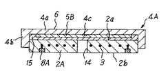
図1は、本発明の実施例に係るウエハー加熱装置1を示す概略部分断面図である。
例えば円盤状のセラミックス基体2の内部には抵抗発熱体3が埋設され、この抵抗発熱体3は好ましくは螺旋状に巻回されている。また、円盤状のセラミックス基体2を平面的にみると、抵抗発熱体3は渦巻形をなすように設置されている。抵抗発熱体3の両端部には、それぞれ電力供給用の端子8が接続、固定され、各端子8の端面が電力供給用ケーブル9に接合されている。一対のケーブル9は、それぞれヒーター電源10に接続されており、図示省略したスイッチを作動させることにより、抵抗発熱体3を発熱させることができる。
【0015】
円盤状セラミックス基体2は、相対向する主面2a,2bを有する。ここで主面とは、他の面よりも相対的に広い面をいう。
【0016】
円盤状セラミックス基体2の一方の主面2aに沿って、例えば円形の膜状電極5が形成されている。そして、この膜状電極5を覆うように、一方の主面2a上にセラミックス誘電体層4が形成され、一体化されている。これにより、膜状電極5は、セラミックス基体2とセラミックス誘電体層4との間に内蔵される。この膜状電極5をパンチングメタルのような穴明きの形状とすると、誘電体層4の密着性が良好となる。セラミックス基体2の内部は端子7が埋設され、この端子7の一端には膜状電極5が接続され、電極端子7の他端にはケーブル11が接続されている。このケーブル11は静電チャック電源12の正極に接続され、直流の電源12の負極がアース線13に接続される。
【0017】
ウエハーWを加熱処理する際には、セラミックス誘電体層4のウエハー吸着面6にウエハーWを設置し、ウエハーWに対してアース線13を接触させる。そして、膜状電極5に正電荷を蓄積してセラミックス誘電体層4を分極させ、セラミックス誘電体層4のウエハー吸着面側に正電荷を蓄積させる。それと共に、ウエハーWの負電荷を蓄積させ、セラミックス誘電体層4とウエハーWとの間のクーロン引力により、ウエハーWをウエハー吸着面6へと吸着させる。これと共に、抵抗発熱体3を発熱させてウエハー吸着面6を所定温度に加熱する。
【0018】
こうしたウエハー加熱装置によれば、ウエハーWをウエハー吸着面6へとクーロン力によって全面で吸着しつつ、同時にウエハー吸着面6を加熱してウエハーを加熱することができる。従って、特に中高真空中でウエハーWを加熱する場合に、ウエハーW全面に亘って温度の追従性が良くなり、ウエハーWを均熱化することができ、ウエハーWとウエハー加熱面との間の隙間によるウエハーWの均熱性の低下が生じない。従って、ウエハーWの熱処理をウエハー全面に亘って均一に行うことができ、例えば半導体製造装置においては、半導体の歩留り低下を防止することができる。
【0019】
また、誘電体層4もセラミックスからなるので、誘電体層4の耐熱性も高く、例えば熱CVD装置において良好に使用できると共に、誘電体層4は、ウエハーの1万回以上のチャックによる磨耗及び変形に対して耐久性を有するセラミックスで形成することが好ましい。
【0020】
更に、セラミックス基体2の内部に抵抗発熱体3が埋設され、また膜状電極5がセラミックス誘電体層4とセラミックス基体2との間に内蔵されているので、従来の金属ヒーターの場合のような汚染を防止できる。また、ウエハーWをウエハー吸着面6へと吸着した状態で直接加熱するので、間接加熱方式の場合のような熱効率の悪化の問題は生じない。
【0021】
誘電体層4をセラミックスにて形成したが、セラミックスは温度が高くなるにつれて絶縁抵抗値(体積固有抵抗)が低くなるという特性があるので、例えば1011Ω・cm程度の適当な絶縁抵抗値よりも低くなり、リーク電流が大きくなりうる。この点で、本実施例の加熱装置1に用いるには、例えば500〜600℃の高温域においても1011Ω・cm以上の絶縁抵抗値を有するものが好ましい。この点で、窒化珪素(反応焼結、常圧焼結)、窒化アルミニウム、サイアロンが好ましい。
【0022】
また、セラミックス基体2、セラミックス誘電体層4は、例えば熱CVD装置においては、最大600℃から1100℃程度まで加熱されるので、通常の耐熱性の観点から、窒化珪素、サイアロン、窒化アルミニウムから形成することが好ましい。
【0023】
窒化珪素、サイアロン、窒化アルミニウムは、アルミナ等の酸化物系セラミックスに比べて、高真空中でのガス放出量が少ない。言い換えると、高真空中でも吸着ガスが少ないことにより、誘電体の抵抗値、耐絶縁破壊電圧等の変化が少なく、ウエハー加熱装置の安定な運転が可能となる。
【0024】
このうち、特に窒化珪素を採用すると、加熱装置1全体の強度が高く、窒化珪素の低熱膨張率のため加熱装置1の耐熱衝撃性が高く、高温での急熱、急冷を繰り返して行っても加熱装置1が破損しない。また、窒化珪素が耐食性に優れていることから、熱CVD装置内等の腐食性ガス条件下でも加熱装置1の耐久性が高く、寿命が長くなる。
【0025】
更に、セラミックス基体2とセラミックス誘電体層4は、密着性の面から熱膨張の等しい同材質とするのが好ましく、ヒーターとしての性能、静電チャックとしての性能の両者の点より、窒化珪素が好ましい。
【0026】
セラミックス基体2の熱膨張率、セラミックス誘電体層4の熱膨張率は、共にウエハーWの熱膨張率の0.7〜1.4倍とすることが好ましい。この範囲外であると、加熱時にウエハーWがウエハー吸着面6に対して密着していることから、ウエハーWに歪みが生ずるおそれがある。こうした材料の組み合わせは、ウエハーWの材料によって変わるべきものである。
【0027】
特に、ウエハーWがシリコン製のときには熱膨張率が2.6×10⁻⁶K-1であり、1.82×10⁻⁶〜3.38×10⁻⁶K-1の範囲とすることが好ましく、窒化珪素は2.7×10⁻⁶K-1であることより、熱膨張率の点からは最もセラミックス基体2、セラミックス誘電体層4の材料に適している。
【0028】
これは、ウエハーWの真空中での吸着力が100g/cm2下では、熱膨張が大きなAl2O3(7×10-6K-1)を使用すると、厚さ0.6mm程度のウエハーが静電チャックに拘束され、0.25%もの変形を受けることが予想される。このため、ウエハーに与える変形のダメージは甚大である。
【0029】
ウエハー吸着面6は平滑面とすることが好ましく、平面度を500μm以下としてウエハーWの裏面へのデポジション用ガスの侵入を防止することが好ましい。抵抗発熱体3としては、高融点でありしかも窒化珪素等との密着性に優れたタングステン、モリブデン、白金等を使用することが適当である。
【0030】
図2は、本発明の実施例に係るウエハー加熱装置の組み立て前の状態を示す断面図、図3はこのウエハー加熱装置を組み立てた後の状態を示す断面図である。本実施例では、平面円形のセラミックス誘電体層4Aを、セラミックスグリーンシートの焼結によって作製する。このセラミックス誘電体層の円盤状本体4aの周縁部には、リング状のフランジ部4bが形成され、フランジ部4bの内側に、円盤形状をした凹部4cが形成されている。
【0031】
また、導電性接合剤からなる円形シート5Aを準備する。これは、後述するように、電極としても機能するものである。また円盤状のセラミックス基体2Aを、セラミックスグリーンシートの焼結によって作製する。セラミックス基体2Aの中央部には、端子挿入用の円形貫通孔14が形成されている。セラミックス基体2Aの一方の主面2aは膜状電極5Aに対向する。セラミックス基体2Aの他方の主面2bに、一対の塊状の端子8Aが露出している。各端子8Aはセラミックス基体2Aに埋設されており、抵抗発熱体3に連結されている。
【0032】
抵抗発熱体3は、円盤状セラミックス基体2Aを平面的にみると、渦巻状のパターンとなるように埋設されている。また、更に細かく見ると、螺旋状に形成されている。また、円柱状の端子7Aを準備する。
セラミックス誘電体層4Aの成形については、プレス成形、テープキャスト成形等を使用できる。セラミックス基体2Aについては、セラミックス材料中に抵抗発熱体3と端子8Aとを埋設し、プレス成形、コールドアイソスタティックプレス成形等を行った後、ホットプレス焼結、ホットアイソスタティックプレス焼結等を行う。
【0033】
そして、膜状電極5Aを凹部4cに収容し、誘電体層4Aの表面に当接させ、更にセラミックス基体2Aの主面2aを膜状電極5Aの表面に当接させる。そして、円柱状端子7Aを貫通孔14に挿通し、その端面7aを膜状電極5Aに当接させる。貫通孔14の壁面と、円柱状端子7Aの側周面との間に、粉末状の接合剤を介在させておく。この状態で、組立体に加熱処理を施し、図3に示すように、導電性接合剤からなる膜状電極5Aによって、誘電体層4Aと基体2Aとを接合する。これと共に、基体2Aの貫通孔14に円柱状端子7Aを接合し、固定する。次いで、誘電体層4Aの表面を研磨加工し、ウエハー吸着面6を平坦にする。
【0034】
円柱状端子7の端面7bにケーブル11を接続し、このケーブルを静電チャック用電源12の正極に接続する。この電源12の負極をアース線13に接続する。
また、各端子8Aにそれぞれケーブル9を接続し、ケーブル9をヒーター電源10に接続する。
【0035】
ウエハーWを吸着する際には、ウエハー吸着面6にウエハーWを設置し、ウエハーWに対してアース線13を接触させる。そして、膜状電極5Aに正電荷を蓄積して誘電体層4Aを分極させ、誘電体層4Aのウエハー吸着面6側に正電荷を蓄積させる。それと共に、ウエハーに負電荷を蓄積させ、誘電体層4AとウエハーWとの間のクーロン引力により、ウエハーをウエハー吸着面6へと吸着させる。これと共に、抵抗発熱体3を発熱させ、ウエハーWを加熱する。
【0036】
図3に示すウエハー加熱装置1Aによれば、記述した効果を奏することができる。また、本実施例においては、焼結した誘電体層4Aと基体2Aを導電性接合剤で接合し、形成された導電性接合剤層をそのまま膜状電極として用いているので、他に電極板等を設ける必要がなく、非常に構造が簡略であり、製造工程も少ない。
【0037】
更に、フランジ部4bを設けたことから、例えば10-3Torr以下の中、高真空条件下においても、膜状電極5Aと半導体ウエハーとの間の放電が生じない。
【0038】
更に、本実施例においては、製法上大きな特徴がある。その点について、順を追って説明する。
本発明者は、図1に示すような構造の加熱装置の製法について多大の検討を加えた。
即ち、まず、図1において、セラミックス基体2のグリーンシートの表面に、膜状電極5をスクリーン印刷によって形成し、その上に薄いセラミックスグリーンシート(誘電体層4用)を積層し、これをプレス成形する方法について検討した。
【0039】
しかしながら、静電チャックの寸法が大きくなると、前記積層品に均等な圧力をかけることは極めて困難であった。従ってこの積層品を焼結しても誘電体層の厚みには不可避的にバラツキが生じた。この誘電体層の厚みは一般的には400μm以下と極めて薄い為、数10μmオーダーのバラツキでも、ウエハー吸着面上でウエハー吸着力にバラツキが生じた。特に誘電体層が相対的に厚い部分では、目標とする吸着力が得られず、ウエハーの反りの矯正が不十分になる場合があった。この一方、誘電体層が相対的に薄い部分では、局所的に絶縁耐圧が低下した。この部分が、製品であるウエハー加熱装置の絶縁耐圧を決定してしまう為、製品全体の絶縁耐圧が著しく低下することがあった。
また、前記積層品を焼結するとき、積層されたグリーンシートの界面で、局所的に密着不良が生じた。これは、焼成収縮が原因と考えられる。
このような密着不良は、走査型電子顕微鏡等によって観察すると、0.1〜数μmオーダーの微小なスキマがある場合が多い。このような加熱装置を半導体製造装置に使用した所、下記のトラブルが生じた。
【0040】
使用条件は、10-3Torr以下の分子流領域の真空下でウエハー温度を450℃にセットした。静電チャックされたウエハーの温度を、赤外線放射温度計にてモニターした所、表面に周囲と温度の異なる局所領域が生じ、必要とする均熱性(±3℃)を確保できず、時によっては、150℃以上の温度差が生じる場合があった。
また最悪条件下では、誘電体層が熱応力によって破壊する場合もあった。
【0041】
本件に関して発明者は、前記シート接合部のスキマについて検討を加えた。その結果、シート接合部のスキマ内の圧力も、半導体製造装置チャンバー内の圧力の影響を受けて変化していた。特に真空中の場合、ガス分子の挙動は大気圧〜1Torrの真空中では粘性流領域にあるが、真空度がさらに高まると分子流領域に移行し、これに伴ってスキマ部の周囲における熱移動がほぼ放射のみによるものとなり、断熱状態となる。このため、スキマ部上の誘電体層の温度が低下し、スキマの無い部分では、熱移動が良好であるため高温を示すことが判った。これにより周囲と温度の異なる局所領域が生じたのである。
【0042】
このように、静電チャックを製造するのに従来採用されていた方法を、図1(又は図3)に示すようなウエハー加熱装置に転用すると、誘電体層の厚さのバラツキや誘電体層とセラミックス基体との界面における密着不良が、不可避的に生じた。この誘電体層の厚さのバラツキも膜状電極の傾斜に起因するものである。従って、一体焼結が終った後に誘電体層の表面を平面研磨加工しても、誘電体層の厚さを均一化することはできないし、むろん上記密着不良を矯正することもできない。
【0043】
ここにおいて、本実施例の方法においては、セラミックスグリーンシートの焼結によって誘電体層4を作製してあるので、その焼結の段階で焼成収縮が終わっており、従って、セラミックス基体2Aと接合する段階ではもう変形しない。
【0044】
このように、本実施例では、誘電体層4Aが変形しないことから、誘電体層4Aの表面を平面加工すれば、誘電体層4Aの厚さを正確に均一化できる。従って、局所的な吸着力の低下や、絶縁耐圧の低下は生じない。また、誘電体層4Aと基体2Aの間には、焼成収縮によるスキマが生じない為、均熱性、耐熱衝撃性に優れる。
【0045】
セラミックス基体2A、誘電体層4Aの材質は、実施例1で述べたものに準ずる。円柱状端子7Aの材質としては、コバール、タングステン、モリブデン、白金、チタン、ニッケル等を例示できる。
導電性接合剤としては、例えば、チタン成分を含む金ろう、チタン成分を含む銀ろう等が好ましい。これは、これらのろう中に含まれるチタンが、加熱処理によってセラミックス中に拡散していくことから、各部材の接合力が大きくなるからである。これらは、特に窒化珪素に対する接合性が良い。また300℃以上で使用される加熱装置では、常温のウエハーが搬送ロボットによって送られてきてチャックされる場合がある。この時誘電体層4Aには、熱衝撃が加わる。導電性接合剤として、軟質金属からなるろう材、たとえばチタン成分を含む金ロウを用いると、ロウ材部材の塑性変形により応力緩和が生じるので、加熱装置の耐熱衝撃性が一層向上する。
【0046】
図2,図3に示す手順に従い、ウエハー加熱装置1Aを作製した。ただし、誘電体層4A、基板2Aをそれぞれ窒化珪素で作成した。これらは、プレス成形体を1800℃で焼結して作成した。端子8A、抵抗発熱体3は、タングステンで形成した。
また、厚さ100μmの円形シート5Aを準備した。この組成は、銀71.3重量%、銅27.9重量%、チタン0.8重量%である。また、これと同材質の粉末状ろうを円柱状端子7Aと貫通孔14との間に介在させた。図2において上下方向に50g/cm2以上の圧力を加えながらこの組立体を熱処理し、ろう付けした。上記したチタン成分を含む銀ろうの酸化を防止するため、ろう付けは10-5Torr以下の圧力の雰囲気下で行った。また、上記熱処理は、900℃で60秒間実施した。この最高温度900℃への昇温及び降温は、セラミックス材料が熱衝撃によって破損しない範囲内において、できるだけ早く行うことが好ましい。本例では、耐熱衝撃性の高い窒化珪素を使用しているので、昇温、降温を600℃/時間の速度で実施した。
【0047】
そして、熱処理後のウエハー加熱装置1Aを加熱炉から取り出し、誘電体層4Aの表面を研摩加工し、その厚さを例えば300μmに調整した。
【0048】
図4〜図8は、本発明の他の実施例に係るウエハー加熱装置1Bの製造手順を説明するための断面図である。図2、図3に示した部材と同一機能を有する部材には同一符号を付け、その説明は省略することがある。
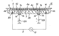
まず、図4に示すように、誘電体層4Aの凹部4c側の表面に、膜状電極5Bを形成する。
【0049】
次いで、図5に示すように、凹部4cに絶縁性接合剤層15を、塗布等によって設ける。この際、膜状電極5Bを、絶縁性接合剤層15によって覆う。
次いで、図6に示すような円盤状の基体2Aを凹部4c内へと挿入し、基体2Aの表面を絶縁性接合剤層15(図5参照)に当接させる。そして、この組立体を熱処理し、図6に示すように、誘電体層4Aの膜状電極5B側の表面と基体2Aの主面2aとを、熱処理後の絶縁性接合剤層15によって接合する。
【0050】
次いで、図7に示すように、貫通孔14の部分で、絶縁性接合剤層15に円形の剥離部15aを設け、膜状電極5Bの表面の一部を貫通孔14に露出させる。
次いで、導電性接合剤からなる粉末を円柱状端子と基体2Aとの間に介在させた状態で熱処理し、図8に示すように、円柱状端子7Aを基体2Aに接合し、円柱状端子7Aの端面7aを膜状電極5Bに当接させる。そして、ウエハー吸着面6を研摩加工する。他は、図2、図3に示した加熱装置と同様である。
【0051】
図4〜図8の手順に従って、実際にウエハー加熱装置1Bを作製した。
ただし、膜状電極5Bは、タングステンのスクリーン印刷によって形成した。また膜状電極5Bを形成した後に、誘電体層4Aを120℃以上に加熱し、印刷した膜中に残留する有機溶媒を蒸発させた。誘電体層4Aおよび基体2Aは、いずれも窒化珪素によって形成した。膜状電極5Bは、モリブデン、白金等で形成してもよい。
【0052】
絶縁性接合剤としては、封着用のガラスを用いた、更に具体的には、下記の組成を有するオキシナイトライドガラスを用いた。
Y2O3 30重量% Al2O3 30重量%
SiO2 30重量% Si3N4 10重量%
【0053】
基体2Aと誘電体層4Aとをガラス封着する際には、50g/cm2以上の圧力で両者を加圧し、窒素雰囲気中1500℃で加熱した。
また、円柱状端子7Aを基体2Aに接合させる際には、銀71.3重量%、銅27.9重量%及びチタン0.8重量%の組成からなるチタン蒸着銀ろうの粉末を用いた。
【0054】
チタン蒸着銀ろうの酸化を防止するため、ろう付けは10-5Torr以下の圧力の雰囲気下で行った。また、上記熱処理は、900℃で60秒間実施した。この最高温度への昇温、降温を600℃/時間の速度で実施した。そして、熱処理後の加熱装置を加熱炉から取り出し、誘電体層4Aの表面を研摩加工し、その厚さを例えば300μmに調整した。端子8A、抵抗発熱体3は、タングステンで形成した。
【0055】
双極型のウエハー加熱装置1cを図9に示す。
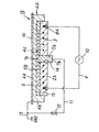
この加熱装置1cにおいては、円盤状セラミックス基体2Bに円形貫通孔14が2つ設けられ、多円形貫通孔14に、それぞれ円柱状端子7Aが挿入され、固定されている。凹部4cの表面には、平面円形の膜状電極5Cが2箇所に形成されている。各膜状電極5Cの中央部付近に、それぞれ端子7Aの端面7aが当接している。図9において左側の端子7Aは、直流電源12Aの負極に接続され、直流電源12Aの正極は接地されている。図9において右側の端子7Aは、直流電源12Bの正極に接続され、直流電源12Bの負極は接地されている。
【0056】
上記の各例ではウエハー吸着面6を上向きにしたが、ウエハー吸着面6を下向きにしてもよい。
上記各例において、加熱装置全体の形状は、円形のウエハーWを均等に加熱するためには円盤状とするのが好ましいが、他の形状、例えば四角盤状、六角盤状等としてもよい。
【0057】
こうした加熱装置は、エピタキシャル装置、プラズマエッチング装置、光エッチング装置等における加熱装置に対しても適用可能である。更に、ウエハーWとしては、半導体ウエハーだけでなく、Alウエハー、Feウエハー等の導体ウエハーの吸着、加熱処理も可能である。
【0058】
【発明の効果】
本発明に係るウエハー吸着加熱装置によれば、抵抗発熱体を埋設したセラミックス基体からなるウエハー加熱装置と、上記セラミックス基体の一方の主面に面状の電極を形成し、この電極を覆うように一方の主面側にセラミックス誘電体層が形成されたウエハー吸着装置とが一体化されているので、ウエハーをセラミックス誘電体層のウエハー吸着面へとクーロン力によって全面で吸着しつつ、同時にウエハー吸着面を介してウエハーを加熱することができる。従って、ウエハー全面に亘って容易に均熱化することができ、ウエハーの加熱時にウエハーとウエハー吸着面(即ちウエハー加熱面)との間に局所的な隙間が生じない。よって、ウエハー全面に亘って加熱処理時の歩留を向上させることができる。
【0059】
また、本発明に係るウエハー吸着装置では、セラミックス基体およびセラミックス誘電体層が、窒化珪素、サイアロンおよび窒化アルミニウムから選ばれ、かつ同種であるので、200℃以上の高温領域においても、誘電体層の絶縁抵抗値、耐絶縁破壊電圧の変化が少ない。さらに電極形状を穴明きとし、セラミックス基体、及び誘電体層とスキマがない状態で接合させているので、10- 3Torr以下の分子流領域の真空下でもウエハーを極めて高い均熱性で200℃以上の高温に加熱できる。したがって、安定した運転が可能であり、ウエハーの歪みも防止できる。
【図面の簡単な説明】
【図1】本発明の実施例に係るウエハー加熱装置1の概略部分断面図である。
【図2】本発明の実施例に係るウエハー加熱装置を組み立てる前の状態を示す断面図である。
【図3】ウエハー加熱装置1Aを示す断面図である。
【図4】誘電体層の凹部4c側の表面に膜状電極5Bを形成した状態を示す断面図である。
【図5】誘電体層の凹部4c側の表面に絶縁性接合剤層15を形成した状態を示す断面図である。
【図6】基体2Aを、絶縁性接合剤層15を介して誘電体層4Aに接合した状態を示す断面図である。
【図7】図6において、絶縁性接合剤層15の一部を剥離させた状態を示す断面図である。
【図8】円柱状端子7Aを基体2Aに接合させた状態を示す断面図である。
【図9】ウエハー加熱装置1Cを示す断面図である。
【符号の説明】
1,1A,1B,1C ウエハー加熱装置
2,2A,2B 円盤状セラミックス基体
2a 一方の主面
3 抵抗発熱体
4,4A セラミックス誘電体層
5,5A,5B,5C 膜状電極
6 ウエハー吸着面
7,7A,8,8A 端子
9,11 ケーブル
10 ヒーター電源
12,12A,12B 静電チャック電源(直流電源)
13 アース線
14 円形貫通孔
15 絶縁性接合剤層
W ウエハー[0001]
BACKGROUND OF THE INVENTION
The present invention relates to a wafer adsorption heating apparatus and a wafer adsorption apparatus for a semiconductor manufacturing apparatus.
[0002]
[Prior art]
In semiconductor manufacturing apparatuses that require a super clean state, corrosive gases such as chlorine-based gases and fluorine-based gases are used as deposition gases, etching gases, and cleaning gases. For this reason, when a conventional heater in which the surface of the resistance heating element is coated with a metal such as stainless steel or Inconel is used as a heating device to heat the wafer in contact with these corrosive gases, By exposure, undesired particles having a particle size of several μm such as chloride, oxide, fluoride, etc. are generated.
[0003]
Therefore, an infrared lamp is installed outside the container that is exposed to the deposition gas, etc., an infrared transmission window is provided on the outer wall of the container, and infrared rays are emitted to the heated object made of a material with good corrosion resistance, such as graphite. An indirect heating type wafer heating apparatus that heats a wafer placed on the upper surface of the body has been developed. However, this method has a larger heat loss than the direct heating type, takes a long time to rise in temperature, and the transmission of infrared rays is gradually hindered by the deposition of a CVD film on the infrared transmission window. There have been problems such as heat absorption by the window and heating of the window, and heat uniformity and response deterioration due to the separation of the heating source and the wafer installation part.
[0004]
[Problems to be solved by the invention]
In order to solve the above problems, a heating apparatus in which a resistance heating element was newly embedded in a disk-shaped dense ceramic was examined. As a result, it has been found that this heating apparatus is an extremely excellent apparatus that has eliminated the above-mentioned problems. However, as the study proceeded, it was found that there was a problem with the method of holding and fixing the semiconductor wafer.
[0005]
That is, as a conventional semiconductor wafer fixing technique, mechanical fixing, vacuum chuck, and electrostatic chuck are known. For example, for semiconductor wafer transfer, exposure, film formation, microfabrication, cleaning, dicing, etc. in use.
[0006]
On the other hand, in particular, in the semiconductor wafer heating and temperature control in film forming processes such as CVD, sputtering, and epitaxial, if the temperature of the heated surface of the semiconductor wafer cannot be made uniform, it causes a decrease in yield during semiconductor production. In this case, with mechanical fixation, film formation becomes non-uniform because pins or rings come into contact with the surface of the semiconductor wafer, and even if the semiconductor wafer is placed on the wafer heating surface of a flat plate-like ceramic heater, the wafer heating Sometimes, the entire surface of the semiconductor wafer is not uniformly suppressed, so that the semiconductor wafer is warped and distorted, and a gap is locally generated between a part of the semiconductor wafer and the flat wafer heating surface. And for example 10-3In medium and high vacuum below Torr, the heat conduction due to gas convection is very small, so the temperature difference between the part of the semiconductor wafer that is in contact with the wafer heating surface and the part where there is a gap is very large. Become.
[0007]
That is, the behavior of gas molecules on the wafer mounting surface is a viscous flow region at a pressure of 1 torr or more, and there is heat transfer (heat transfer) by gas molecules. Accordingly, the wafer temperature does not decrease much with respect to the heater temperature even in the portion where the gap is generated, and good followability is exhibited. However, when a medium or high vacuum is reached, the behavior of gas molecules shifts to the molecular flow region, and the heat transfer due to gas molecules is greatly reduced, so the wafer temperature decreases with respect to the heater temperature, resulting in poor thermal uniformity and responsiveness. I found out.
[0008]
Also, so-called vacuum chucks cannot be used under medium and high vacuum conditions such as sputtering and CVD equipment.
[0009]
Furthermore, in the so-called electrostatic chuck, a polyimide film or the like is used as a dielectric film, and the operating temperature range of the conventional electrostatic chuck is about 80 ° to 200 ° C. at the maximum. For this reason, it cannot be installed in a heating device that can be used up to about 600 ° C. for heating the sputtering and CVD devices.
[0010]
In addition, it has been found that in a high temperature region of 200 ° C. or higher in which a heater is normally used, the insulation resistance value and dielectric breakdown voltage of the dielectric layer are remarkably changed, and stable operation is difficult.
An object of the present invention is to provide a wafer heating apparatus capable of preventing the problem of contamination as in the case of a metal heater and the deterioration of thermal efficiency as in the case of an indirect heating method and improving the temperature uniformity of the wafer to be heated. Is to provide. In addition, in a high temperature region of 200 ° C. or higher, it is possible to suppress a change in the insulation resistance value and dielectric breakdown voltage of the dielectric layer and to enable stable operation. Moreover, it is providing the wafer adsorption | suction apparatus applicable to such a wafer heating apparatus.
[0011]
[Means for Solving the Problems]
The wafer adsorption heating device of the present invention isTheAn apparatus for heating the wafer while adsorbing air, formed on a main surface of a base made of a ceramic sintered body, a resistance heating element embedded in the base, and the baseFor adsorbing wafersIt has an electrode and a dielectric layer made of a ceramic sintered body formed on one main surface side so as to cover the electrode, and the resistance is maintained while the wafer is adsorbed to the wafer adsorption surface of the dielectric layer. The wafer is configured to be heated by the heat generated by the heating element, and the material of the substrate and the dielectric layer is made of one or more kinds of ceramics selected from the group consisting of silicon nitride, sialon and aluminum nitride, The electrode has a planar perforated shape and must be bonded to the substrate and dielectric layer without any gaps.To ensure uniform heat uniformity of the waferIt is characterized by.
[0012]
In addition, the wafer adsorption device of the present invention is formed on a substrate made of a ceramic sintered body and one main surface of the substrate.For adsorbing wafersAn electrode and a dielectric layer made of a ceramic sintered body formed on one main surface so as to cover the electrode, and the material of the base and the dielectric layer is silicon nitride, sialon, and aluminum nitride It is made of one or more kinds of the same kind of ceramics selected from the group consisting of: the electrode has a planar perforated shape, and is joined to the substrate and the dielectric layer without any gap.To ensure uniform heat uniformity of the waferIt is characterized by.
[0013]
[Embodiments of the Invention]
A wafer adsorption heating device according to an embodiment of the present invention includes a wafer heating device having a base made of a ceramic sintered body, a resistance heating element embedded in the base, a base made of a ceramic sintered body, A wafer adsorbing device having an electrode formed on one main surface of the substrate and a dielectric layer made of a ceramic sintered body formed on one main surface so as to cover the electrode is integrally formed. It has become. In the integration, the substrate made of the ceramic sintered body constituting the wafer heating device and the substrate made of the ceramic sintered body constituting the wafer adsorbing device may be the same.
Further, in the wafer adsorption device according to the present embodiment, the base material and the dielectric layer are made of one or more kinds of ceramics selected from the group consisting of silicon nitride, sialon, and aluminum nitride, It is characterized in that it is joined to the dielectric layer without any gap. This electrode has at least a planar shape including film-like, sheet-like and plate-like electrodes, and has a perforated shape so that there is no gap on the joint surface between the substrate and the dielectric layer. The structure is easy to form. Note that the gap in the present application is, for example, a fine enough to inevitably remain on the sheet bonding surface when a laminated molded body or the like produced by, for example, laminating a plurality of green sheets and pressing them is subjected to normal pressure sintering. Including a gap. Therefore, the wafer suction apparatus according to the present embodiment preferably does not have a minute gap on the order of 0.1 to several μm.
Since the wafer adsorption heating device according to the present embodiment has no gap between the electrode, substrate, and dielectric layer of the wafer adsorption device integrated with the wafer heating device, 10-3Even if the wafer is heated to a high temperature of 200 ° C. or higher under vacuum in a molecular flow region of Torr or lower, extremely high temperature uniformity can be secured.
As a method for producing such a wafer adsorption heating device without a gap, for example, the following production method can be cited.
At least a resistance heating element is embedded in the ceramic green sheet and sintered to produce a ceramic substrate in which the resistance heating element is embedded, and a ceramic dielectric sheet is prepared by sintering the ceramic green sheet. One main surface of the electrode and the ceramic dielectric layer are joined by a film-like electrode made of a conductive bonding agent, and a terminal is connected to the film-like electrode.
Moreover, at least a resistance heating element is embedded and sintered inside the ceramic green sheet to produce a ceramic substrate in which the resistance heating element is embedded, and the ceramic green sheet is sintered to produce a ceramic dielectric layer. A film electrode is formed on the surface of the ceramic dielectric layer, and one main surface of the ceramic substrate and the film electrode side surface of the ceramic dielectric layer are bonded with an insulating bonding agent, and a terminal is connected to the film electrode. Connecting.
The ceramic substrate in which the resistance heating element is embedded can be manufactured by hot press sintering or hot isostatic press sintering. Further, the ceramic dielectric layer and the planar electrode may be integrally sintered with the ceramic substrate by hot press sintering or hot isostatic press sintering.
[0014]
【Example】
FIG. 1 is a schematic partial sectional view showing a wafer heating apparatus 1 according to an embodiment of the present invention.
For example, a
[0015]
The disk-shaped
[0016]
For example, a
[0017]
When the wafer W is heat-treated, the wafer W is placed on the
[0018]
According to such a wafer heating apparatus, the wafer W can be heated by simultaneously heating the
[0019]
In addition, since the dielectric layer 4 is also made of ceramics, the dielectric layer 4 has high heat resistance, and can be used well in, for example, a thermal CVD apparatus. It is preferable to form with a ceramic having durability against deformation.
[0020]
Further, since the
[0021]
Although the dielectric layer 4 is formed of ceramics, ceramics has a characteristic that the insulation resistance value (volume resistivity) decreases as the temperature increases.11It becomes lower than an appropriate insulation resistance value of about Ω · cm, and the leakage current can be increased. In this respect, for use in the heating device 1 of the present embodiment, for example, even in a high temperature range of 500 to 600 ° C., 1011Those having an insulation resistance value of Ω · cm or more are preferable. In this respect, silicon nitride (reaction sintering, normal pressure sintering), aluminum nitride, and sialon are preferable.
[0022]
The
[0023]
Silicon nitride, sialon, and aluminum nitride emit less gas in high vacuum than oxide ceramics such as alumina. In other words, since the amount of adsorbed gas is small even in a high vacuum, there is little change in the dielectric resistance, dielectric breakdown voltage, etc., and the wafer heating apparatus can be operated stably.
[0024]
Among these, when silicon nitride is employed, the strength of the entire heating device 1 is high, the thermal shock resistance of the heating device 1 is high due to the low thermal expansion coefficient of silicon nitride, and rapid heating and rapid cooling at high temperatures can be repeated. The heating device 1 is not damaged. Moreover, since silicon nitride is excellent in corrosion resistance, the durability of the heating device 1 is high and the life is extended even under corrosive gas conditions such as in a thermal CVD apparatus.
[0025]
Further, the
[0026]
The thermal expansion coefficient of the
[0027]
In particular, when the wafer W is made of silicon, the coefficient of thermal expansion is 2.6 × 10.-6K-1And 1.82 × 10⁻⁶~ 3.38 × 10⁻⁶K-1Preferably, silicon nitride is 2.7 × 10⁻⁶K-1Therefore, it is most suitable for the material of the
[0028]
This is because the suction force of the wafer W in vacuum is 100 g / cm.2Below, Al with large thermal expansion2OThree(7 × 10⁻⁶K-1), A wafer having a thickness of about 0.6 mm is constrained by the electrostatic chuck and is expected to be deformed by 0.25%. For this reason, the deformation damage to the wafer is enormous.
[0029]
The
[0030]
FIG. 2 is a cross-sectional view showing a state before the wafer heating apparatus according to the embodiment of the present invention is assembled, and FIG. 3 is a cross-sectional view showing a state after the wafer heating apparatus is assembled. In this embodiment, the planar circular ceramic
[0031]
In addition, a
[0032]
The
For forming the
[0033]
Then, the film-
[0034]
A
Further, the
[0035]
When sucking the wafer W, the wafer W is set on the
[0036]
According to the wafer heating apparatus 1A shown in FIG. 3, the described effects can be obtained. In the present embodiment, the sintered
[0037]
Further, since the
[0038]
Furthermore, the present embodiment has a significant feature in the manufacturing method. This will be explained in order.
The present inventor has made extensive studies on the manufacturing method of the heating apparatus having the structure shown in FIG.
That is, first, in FIG. 1, a film-
[0039]
However, when the size of the electrostatic chuck is increased, it is extremely difficult to apply a uniform pressure to the laminated product. Therefore, even when this laminate was sintered, the thickness of the dielectric layer inevitably varied. Since the thickness of the dielectric layer is generally very thin, 400 μm or less, even if the variation is on the order of several tens of μm, the wafer attracting force varies on the wafer attracting surface. In particular, in a portion where the dielectric layer is relatively thick, a target adsorption force cannot be obtained, and correction of the warpage of the wafer may be insufficient. On the other hand, the withstand voltage locally decreased in the portion where the dielectric layer was relatively thin. Since this portion determines the dielectric strength of the wafer heating device as a product, the dielectric strength of the entire product may be significantly reduced.
Further, when the laminated product was sintered, adhesion failure locally occurred at the interface of the laminated green sheets. This is considered to be caused by firing shrinkage.
Such adhesion defects often have minute gaps on the order of 0.1 to several μm when observed with a scanning electron microscope or the like. When such a heating apparatus was used in a semiconductor manufacturing apparatus, the following trouble occurred.
[0040]
Use condition is 10-3The wafer temperature was set at 450 ° C. under vacuum in the molecular flow region below Torr. When the temperature of the electrostatic chucked wafer was monitored with an infrared radiation thermometer, a local region with a different temperature from the surroundings was generated on the surface, and the required thermal uniformity (± 3 ° C) could not be ensured. In some cases, a temperature difference of 150 ° C. or more occurred.
Also, under the worst conditions, the dielectric layer may be destroyed by thermal stress.
[0041]
In this regard, the inventor has examined the clearance at the sheet joint. As a result, the pressure in the gap at the sheet bonding portion also changed under the influence of the pressure in the semiconductor manufacturing apparatus chamber. Especially in vacuum, the behavior of gas molecules is in the viscous flow region in the vacuum of atmospheric pressure to 1 Torr, but when the degree of vacuum further increases, it moves to the molecular flow region, and accordingly heat transfer around the skimmer part. Becomes almost due to radiation only, and becomes adiabatic. For this reason, it has been found that the temperature of the dielectric layer on the gap portion decreases, and the portion without the gap has a high temperature because heat transfer is good. As a result, local regions having different temperatures from the surroundings were generated.
[0042]
As described above, when the method conventionally used for manufacturing the electrostatic chuck is diverted to the wafer heating apparatus as shown in FIG. 1 (or FIG. 3), the variation in the thickness of the dielectric layer and the dielectric layer Inadequate adhesion at the interface between the ceramic substrate and the ceramic substrate inevitably occurred. The variation in the thickness of the dielectric layer is also caused by the inclination of the film electrode. Therefore, even if the surface of the dielectric layer is subjected to planar polishing after the integral sintering, the thickness of the dielectric layer cannot be made uniform, and of course, the above adhesion failure cannot be corrected.
[0043]
Here, in the method of this example, since the dielectric layer 4 is produced by sintering the ceramic green sheet, the firing shrinkage is finished at the stage of the sintering, and hence the
[0044]
Thus, in this embodiment, since the
[0045]
The materials of the
As the conductive bonding agent, for example, a gold brazing containing a titanium component, a silver brazing containing a titanium component, and the like are preferable. This is because titanium contained in these waxes diffuses into the ceramics by the heat treatment, so that the bonding force of each member increases. These have particularly good bonding properties to silicon nitride. In a heating apparatus used at 300 ° C. or higher, a normal temperature wafer may be sent and chucked by a transfer robot. At this time, a thermal shock is applied to the
[0046]
A wafer heating apparatus 1A was produced according to the procedure shown in FIGS. However, the
A
[0047]
Then, the wafer heating apparatus 1A after the heat treatment was taken out from the heating furnace, the surface of the
[0048]
4-8 is sectional drawing for demonstrating the manufacturing procedure of the wafer heating apparatus 1B which concerns on the other Example of this invention. Members having the same functions as those shown in FIGS. 2 and 3 are denoted by the same reference numerals, and the description thereof may be omitted.
First, as shown in FIG. 4, a
[0049]
Next, as shown in FIG. 5, an insulating
Next, a disc-shaped
[0050]
Next, as shown in FIG. 7, a circular peeling portion 15 a is provided in the insulating
Next, heat treatment is performed with the powder composed of the conductive bonding agent interposed between the cylindrical terminal and the
[0051]
A wafer heating apparatus 1B was actually manufactured according to the procedure of FIGS.
However, the
[0052]
As the insulating bonding agent, sealing glass was used, more specifically, oxynitride glass having the following composition was used.
Y2OThree 30 wt% Al2OThree 30% by weight
SiO2 30 wt% SiThreeNFour 10% by weight
[0053]
When the
Further, when the
[0054]
To prevent oxidation of the titanium-deposited silver braze, brazing is 10-FiveThe test was carried out in an atmosphere with a pressure equal to or lower than Torr. The heat treatment was performed at 900 ° C. for 60 seconds. The temperature was raised and lowered to the maximum temperature at a rate of 600 ° C./hour. And the heating apparatus after heat processing was taken out from the heating furnace, the surface of the
[0055]
A bipolar wafer heating apparatus 1c is shown in FIG.
In this heating device 1c, two circular through
[0056]
In each of the above examples, the
In each of the above examples, the shape of the entire heating device is preferably a disc shape in order to uniformly heat the circular wafer W, but may be another shape such as a square disc shape or a hexagonal disc shape.
[0057]
Such a heating device can also be applied to a heating device in an epitaxial device, a plasma etching device, a photoetching device, or the like. Further, as the wafer W, not only a semiconductor wafer but also a conductive wafer such as an Al wafer and an Fe wafer can be adsorbed and heat-treated.
[0058]
【The invention's effect】
According to the wafer adsorption heating device of the present invention, a wafer heating device composed of a ceramic substrate in which a resistance heating element is embedded, and a planar electrode is formed on one main surface of the ceramic substrate so as to cover the electrode. Since the wafer adsorption device with ceramic dielectric layer formed on one main surface is integrated, the wafer is adsorbed to the wafer adsorption surface of the ceramic dielectric layer on the whole surface by Coulomb force and at the same time wafer adsorption The wafer can be heated through the surface. Therefore, the temperature can be easily equalized over the entire surface of the wafer, and no local gap is generated between the wafer and the wafer suction surface (ie, the wafer heating surface) when the wafer is heated. Therefore, the yield during the heat treatment can be improved over the entire wafer surface.
[0059]
In the wafer adsorption device according to the present invention, the ceramic substrate and the ceramic dielectric layer are selected from silicon nitride, sialon, and aluminum nitride and are of the same type. Therefore, even in a high temperature region of 200 ° C. or higher, Little change in insulation resistance and breakdown voltage. Furthermore, since the electrode shape is perforated and bonded to the ceramic substrate and the dielectric layer without any gaps, 10- 3The wafer can be heated to a high temperature of 200 ° C. or higher with extremely high temperature uniformity even under a vacuum of a molecular flow region below Torr. Therefore, stable operation is possible and wafer distortion can be prevented.
[Brief description of the drawings]
FIG. 1 is a schematic partial sectional view of a wafer heating apparatus 1 according to an embodiment of the present invention.
FIG. 2 is a cross-sectional view showing a state before the wafer heating apparatus according to the embodiment of the present invention is assembled.
FIG. 3 is a cross-sectional view showing a wafer heating apparatus 1A.
FIG. 4 is a cross-sectional view showing a state in which a film-
FIG. 5 is a cross-sectional view showing a state in which an insulating
6 is a cross-sectional view showing a state in which a
7 is a cross-sectional view showing a state where a part of the insulating
FIG. 8 is a cross-sectional view showing a state in which a
FIG. 9 is a cross-sectional view showing a wafer heating apparatus 1C.
[Explanation of symbols]
1,1A, 1B, 1C Wafer heating device
2,2A, 2B Disc-shaped ceramic substrate
2a One main surface
3 resistance heating elements
4,4A Ceramic dielectric layer
5,5A, 5B, 5C Membrane electrode
6 Wafer suction surface
7,7A, 8,8A terminal
9,11 cable
10 Heater power supply
12, 12A, 12B Electrostatic chuck power supply (DC power supply)
13 Ground wire
14 circular through hole
15 Insulating adhesive layer
W wafer
Claims (7)
セラミックス焼結体からなる基体と、
前記基体の内部に埋設された抵抗発熱体と、
前記基体の一方の主面上に形成され、前記ウエハーを吸着するための電極と、
前記電極を覆うように前記一方の主面側に形成されたセラミックス焼結体からなる誘電体層とを有しており、
前記誘電体層のウエハー吸着面へと前記ウエハーを吸着した状態で、前記抵抗発熱体の発熱によりこのウエハーを加熱しうるように構成されており、前記基体及び前記誘電体層の材質が、窒化珪素、サイアロン及び窒化アルミニウムからなる群より選ばれた一種以上の同種のセラミックスからなり、
前記電極は、面状の穴明き形状を有し、前記基体及び前記誘電体層と、スキマがない状態で接合していることにより、前記ウエハーの均熱性を確保することを特徴とするウエハー吸着加熱装置。While adsorbing c Eha An apparatus for heating the wafer,
A substrate made of a ceramic sintered body;
A resistance heating element embedded in the substrate;
An electrode formed on one main surface of the substrate and for adsorbing the wafer ;
A dielectric layer made of a ceramic sintered body formed on the one main surface side so as to cover the electrode;
The wafer can be heated by the heat generated by the resistance heating element in a state where the wafer is attracted to the wafer adsorption surface of the dielectric layer, and the material of the base and the dielectric layer is nitrided. Consisting of one or more similar ceramics selected from the group consisting of silicon, sialon and aluminum nitride,
The electrode has a planar perforated shape, and is bonded to the base body and the dielectric layer in a state without a gap, thereby ensuring the thermal uniformity of the wafer. Adsorption heating device.
前記基体の一方の主面上に形成され、ウエハーを吸着するための電極と、
前記電極を覆うように前記一方の主面側に形成されたセラミックス焼結体からなる誘電体層とを有しており、
前記基体及び前記誘電体層の材質は、窒化珪素、サイアロン及び窒化アルミニウムからなる群より選ばれた一種以上の同種のセラミックスからなり、
前記電極は、面状の穴明き形状を有し、前記基体及び前記誘電体層と、スキマがない状態で接合していることにより、前記ウエハーの均熱性を確保することを特徴とするウエハー吸着装置。A substrate made of a ceramic sintered body;
An electrode formed on one main surface of the substrate and for adsorbing a wafer ;
A dielectric layer made of a ceramic sintered body formed on the one main surface side so as to cover the electrode;
The base material and the dielectric layer are made of one or more kinds of ceramics selected from the group consisting of silicon nitride, sialon and aluminum nitride,
The electrode has a planar perforated shape, and is bonded to the base body and the dielectric layer in a state without a gap, thereby ensuring the thermal uniformity of the wafer. Adsorption device.
Priority Applications (1)
| Application Number | Priority Date | Filing Date | Title |
|---|---|---|---|
| JP2003077578A JP3662909B2 (en) | 1990-12-25 | 2003-03-20 | Wafer adsorption heating device and wafer adsorption device |
Applications Claiming Priority (3)
| Application Number | Priority Date | Filing Date | Title |
|---|---|---|---|
| JP41800690 | 1990-12-25 | ||
| JP2-418006 | 1990-12-25 | ||
| JP2003077578A JP3662909B2 (en) | 1990-12-25 | 2003-03-20 | Wafer adsorption heating device and wafer adsorption device |
Related Parent Applications (1)
| Application Number | Title | Priority Date | Filing Date |
|---|---|---|---|
| JP2000385426A Division JP3699349B2 (en) | 1990-12-25 | 2000-12-19 | Wafer adsorption heating device |
Publications (2)
| Publication Number | Publication Date |
|---|---|
| JP2003347396A JP2003347396A (en) | 2003-12-05 |
| JP3662909B2 true JP3662909B2 (en) | 2005-06-22 |
Family
ID=29781726
Family Applications (1)
| Application Number | Title | Priority Date | Filing Date |
|---|---|---|---|
| JP2003077578A Expired - Lifetime JP3662909B2 (en) | 1990-12-25 | 2003-03-20 | Wafer adsorption heating device and wafer adsorption device |
Country Status (1)
| Country | Link |
|---|---|
| JP (1) | JP3662909B2 (en) |
Families Citing this family (7)
| Publication number | Priority date | Publication date | Assignee | Title |
|---|---|---|---|---|
| JP4744855B2 (en) * | 2003-12-26 | 2011-08-10 | 日本碍子株式会社 | Electrostatic chuck |
| JP5046529B2 (en) * | 2005-02-25 | 2012-10-10 | 株式会社半導体エネルギー研究所 | Semiconductor device |
| JP5154871B2 (en) * | 2006-09-13 | 2013-02-27 | 日本碍子株式会社 | Electrostatic chuck and manufacturing method thereof |
| JP5298430B2 (en) * | 2007-01-11 | 2013-09-25 | 住友電気工業株式会社 | Semiconductor heating device |
| JP6629624B2 (en) * | 2016-02-17 | 2020-01-15 | 日本特殊陶業株式会社 | Manufacturing method of ceramic heater |
| JP6738748B2 (en) * | 2017-02-08 | 2020-08-12 | 日本特殊陶業株式会社 | Ceramic heater manufacturing method |
| CN109935540B (en) * | 2019-03-12 | 2024-06-18 | 上海至纯洁净系统科技股份有限公司 | A gripper with heating function and wet tank cleaning equipment |
Family Cites Families (7)
| Publication number | Priority date | Publication date | Assignee | Title |
|---|---|---|---|---|
| JPS6286837A (en) * | 1985-10-14 | 1987-04-21 | Tokyo Electron Ltd | Wafer conveyor |
| JPS62286248A (en) * | 1986-06-05 | 1987-12-12 | Toto Ltd | Electrostatic chuck plate and manufacture thereof |
| JPH0719831B2 (en) * | 1986-10-13 | 1995-03-06 | 日本電信電話株式会社 | Electrostatic check |
| JP2535372B2 (en) * | 1988-03-09 | 1996-09-18 | 日本碍子株式会社 | Ceramic heater, electrochemical device and oxygen analyzer |
| JP2582410B2 (en) * | 1988-04-26 | 1997-02-19 | 東陶機器株式会社 | Electrostatic chuck substrate |
| JPH0243134U (en) * | 1988-09-13 | 1990-03-26 | ||
| JPH0746437Y2 (en) * | 1989-04-17 | 1995-10-25 | 東陶機器株式会社 | Electrostatic chuck |
-
2003
- 2003-03-20 JP JP2003077578A patent/JP3662909B2/en not_active Expired - Lifetime
Also Published As
| Publication number | Publication date |
|---|---|
| JP2003347396A (en) | 2003-12-05 |
Similar Documents
| Publication | Publication Date | Title |
|---|---|---|
| JP3699349B2 (en) | Wafer adsorption heating device | |
| US5280156A (en) | Wafer heating apparatus and with ceramic substrate and dielectric layer having electrostatic chucking means | |
| JP4744855B2 (en) | Electrostatic chuck | |
| US5535090A (en) | Electrostatic chuck | |
| JP6064908B2 (en) | Electrostatic chuck device | |
| KR102369706B1 (en) | Electrostatic chuck and method of making same | |
| JP3457477B2 (en) | Electrostatic chuck | |
| KR100648327B1 (en) | Electrostatic chuck formed by sintering ceramic and metal integrally | |
| WO2000072376A1 (en) | Electrostatic chuck and treating device | |
| JPH08227933A (en) | Wafer heating device with electrostatic adsorption function | |
| CN111446197B (en) | Electrostatic chuck and electrostatic chuck device including same | |
| JP2012510157A (en) | Electrostatic chuck | |
| JPH0750736B2 (en) | Wafer heating apparatus and manufacturing method thereof | |
| JP2016058748A (en) | Electrostatic chuck device | |
| JP3662909B2 (en) | Wafer adsorption heating device and wafer adsorption device | |
| JPH04304941A (en) | Manufacture of wafer holder | |
| JP3586034B2 (en) | Electrostatic chuck | |
| TW202410287A (en) | Electrostatic chuck and semiconductor process equipment | |
| JP3348140B2 (en) | Electrostatic chuck | |
| JP2836986B2 (en) | Electrostatic chuck and method of manufacturing the same | |
| JP3767719B2 (en) | Electrostatic chuck | |
| JPH07273175A (en) | Holding member | |
| JP2001077185A (en) | Electrostatic chuck and method of manufacturing the same | |
| JPH06279974A (en) | Susceptor for production of semiconductor | |
| JP6642170B2 (en) | Electrostatic chuck device and manufacturing method thereof |
Legal Events
| Date | Code | Title | Description |
|---|---|---|---|
| A131 | Notification of reasons for refusal |
Free format text: JAPANESE INTERMEDIATE CODE: A131 Effective date: 20040831 |
|
| A521 | Written amendment |
Free format text: JAPANESE INTERMEDIATE CODE: A523 Effective date: 20041101 |
|
| A521 | Written amendment |
Free format text: JAPANESE INTERMEDIATE CODE: A523 Effective date: 20041116 |
|
| TRDD | Decision of grant or rejection written | ||
| A01 | Written decision to grant a patent or to grant a registration (utility model) |
Free format text: JAPANESE INTERMEDIATE CODE: A01 Effective date: 20050322 |
|
| A61 | First payment of annual fees (during grant procedure) |
Free format text: JAPANESE INTERMEDIATE CODE: A61 Effective date: 20050324 |
|
| R150 | Certificate of patent or registration of utility model |
Free format text: JAPANESE INTERMEDIATE CODE: R150 |
|
| FPAY | Renewal fee payment (event date is renewal date of database) |
Free format text: PAYMENT UNTIL: 20090401 Year of fee payment: 4 |
|
| FPAY | Renewal fee payment (event date is renewal date of database) |
Free format text: PAYMENT UNTIL: 20100401 Year of fee payment: 5 |
|
| FPAY | Renewal fee payment (event date is renewal date of database) |
Free format text: PAYMENT UNTIL: 20100401 Year of fee payment: 5 |
|
| FPAY | Renewal fee payment (event date is renewal date of database) |
Free format text: PAYMENT UNTIL: 20110401 Year of fee payment: 6 |
|
| FPAY | Renewal fee payment (event date is renewal date of database) |
Free format text: PAYMENT UNTIL: 20110401 Year of fee payment: 6 |
|
| FPAY | Renewal fee payment (event date is renewal date of database) |
Free format text: PAYMENT UNTIL: 20120401 Year of fee payment: 7 |
|
| EXPY | Cancellation because of completion of term | ||
| FPAY | Renewal fee payment (event date is renewal date of database) |
Free format text: PAYMENT UNTIL: 20120401 Year of fee payment: 7 |