JP3661489B2 - MPU mounting structure - Google Patents
MPU mounting structure Download PDFInfo
- Publication number
- JP3661489B2 JP3661489B2 JP14742999A JP14742999A JP3661489B2 JP 3661489 B2 JP3661489 B2 JP 3661489B2 JP 14742999 A JP14742999 A JP 14742999A JP 14742999 A JP14742999 A JP 14742999A JP 3661489 B2 JP3661489 B2 JP 3661489B2
- Authority
- JP
- Japan
- Prior art keywords
- mpu
- board
- mounting structure
- connector
- casing
- Prior art date
- Legal status (The legal status is an assumption and is not a legal conclusion. Google has not performed a legal analysis and makes no representation as to the accuracy of the status listed.)
- Expired - Fee Related
Links
Images

Classifications
-
- H—ELECTRICITY
- H01—ELECTRIC ELEMENTS
- H01L—SEMICONDUCTOR DEVICES NOT COVERED BY CLASS H10
- H01L2224/00—Indexing scheme for arrangements for connecting or disconnecting semiconductor or solid-state bodies and methods related thereto as covered by H01L24/00
- H01L2224/01—Means for bonding being attached to, or being formed on, the surface to be connected, e.g. chip-to-package, die-attach, "first-level" interconnects; Manufacturing methods related thereto
- H01L2224/10—Bump connectors; Manufacturing methods related thereto
- H01L2224/15—Structure, shape, material or disposition of the bump connectors after the connecting process
- H01L2224/16—Structure, shape, material or disposition of the bump connectors after the connecting process of an individual bump connector
Description
【0001】
【発明の属する技術分野】
本発明は、MPU(Micro Processing Uintの略)を電子装置の金属筐体内側に実装するための、MPUの実装構造に関する。
【0002】
【従来の技術】
MPUには、高集積化された電子回路が高密度に形成されていて、その動作時の発熱量が、メモリチップ等と比べて、数段に大きい。
そのため、電子装置においては、そのMPUが発する熱をMPU外部に効率良く放散させる必要がある。そして、MPUが、自己の発する熱により高熱に晒されて、誤動作したり動作不能に陥ったりするのを防ぐ必要がある。
【0003】
このMPUが発する熱をMPU外部に効率良く放散させる手段としては、従来より、大別して、MPUの近くに設けた冷却ファンにより、MPU周囲に冷却用の空気を強制循環させる方式のものと、MPUに高熱伝導性の金属からなるヒートスプレッダを装着して、そのヒートスプレッダにMPUが発する熱を放散させる自然対流方式のものと、さらには、MPUに装着したヒートスプレッダにヒートパイプを付設して、そのヒートパイプ中を循環する冷媒の蒸発潜熱によりヒートスプレッダを介してMPUを強制冷却する方式のものとがある。
【0004】
【発明が解決しようとする課題】
しかしながら、上記のMPU冷却用の、冷却ファン、ヒートスプレッダ、又はそれに加えてヒートパイプを電子装置の筐体内側に備えた場合には、その分、それを収容した筐体の容積が増して、MPUが内蔵された電子装置の小型化、薄型化、軽量化を図れなかった。
このことは、特に、その薄型化、小型化、軽量化が要求されるノート型のパソコン等の電子装置において顕著であった。
【0005】
そこで、本発明者は、鋭意研究の結果、近時のノート型のパソコン等の電子装置の筐体には、そのリサイクル化を図るために、樹脂と金属との組み合わせからなるハイブリッド筐体が用いられており、そのハイブリッド筐体のAl、Al合金、Mg又はMg合金等からなる高熱伝導性の金属筐体を、上記のMPUが発する熱を放散させるヒートスプレッダに代用できることを、発見した。また、その金属筐体をヒートスプレッダに用いれば、筐体内側に備えるMPU冷却用のヒートスプレッダや冷却ファン等を排除でき、その分、電子装置の小型化、薄型化、軽量化が図れることを発見した。そして、そのハイブリッド筐体等の金属筐体をヒートスプレッダに用いた、新たなMPUの実装構造を開発した。
【0006】
即ち、本発明は、電子装置の金属筐体をヒートスプレッダに用いた、MPUの実装構造を提供することを目的としている。
【0007】
【課題を解決するための手段】
上記の目的を達成するために、本発明の第1のMPUの実装構造は、MPUとプリント基板とが金属筺体内側に備えられた電子装置において、前記MPUが下面に実装されたフレキシブル基板の下方に、透孔が設けられた前記プリント基板が、フレキシブル基板とほぼ平行に対向させて配置され、そのフレキシブル基板の下面とプリント基板の上面とには、コネクタが備えられて、そのコネクタを介して前記フレキシブル基板とプリント基板とが電気的に接続され、前記MPUが、前記プリント基板の透孔を通して、その下方の電子装置の金属筐体部分に固定されると共に、MPUとコネクタとの間に位置する前記フレキシブル基板部分が、前記金属筐体に固定されたMPUの上面と前記プリント基板の上面側に備えられたコネクタの上面との高低差に合わせて、上下方向に折曲されてなることを特徴としている。
【0008】
また、上記の目的を達成するために、本発明の第2のMPUの実装構造は、MPUとプリント基板とが金属筺体内側に備えられた電子装置において、前記プリント基板の下方に、前記MPUが下面に実装されたフレキシブル基板が、プリント基板とほぼ平行に対向させて配置され、そのフレキシブル基板の上面とプリント基板の下面とには、コネクタが備えられて、そのコネクタを介して前記プリント基板とフレキシブル基板とが電気的に接続され、前記MPUが、その下方の電子装置の金属筐体部分に固定されると共に、MPUとコネクタとの間に位置する前記フレキシブル基板部分が、前記金属筐体に固定されたMPUの上面と前記プリント基板の下面側に備えられたコネクタの下面との高低差に合わせて、上下方向に折曲されてなることを特徴としている。
【0009】
この第1又は第2のMPUの実装構造においては、MPUが固定された高熱伝導性の金属筐体に、MPUが発する熱を効率良く放散させることができる。
【0010】
第1のMPUの実装構造にあっては、MPUが、プリント基板に設けられた透孔を通して、その下方の金属筐体部分に固定されているため、そのプリント基板に設けられた透孔の内側空間を有効利用して、プリント基板の厚さ分、MPUを金属筐体内側にコンパクトに丈低く収容できる。
【0011】
また、金属筐体に固定されたMPUの上面とコネクタの上面との高低差に合わせて、そのMPUとコネクタとの間に位置するフレキシブル基板部分を上下方向に折曲させることができる。そして、そのフレキシブル基板とコネクタとを介して、MPUをプリント基板に容易かつ的確に電気的に接続できる。
【0012】
第2のMPUの実装構造にあっては、プリント基板とフレキシブル基板とを電気的に接続するコネクタが備えられたプリント基板と金属筐体との間の内側空間を有効利用して、その内側空間にMPUをコンパクトに丈低く収容できる。
【0013】
また、金属筐体に固定されたMPUの上面とコネクタの下面との高低差に合わせて、そのMPUとコネクタとの間に位置するフレキシブル基板部分を上下方向に折曲させることができる。そして、そのフレキシブル基板とコネクタとを介して、MPUをプリント基板に容易かつ的確に電気的に接続できる。
【0014】
本発明の第1又は第2のMPUの実装構造においては、前記MPUが固定された金属筐体部分側とは反対側の金属筐体外側部分に、低熱伝導体が埋設された構造とすることを好適としている。
【0015】
この第1又は第2のMPUの実装構造にあっては、MPUが発する熱を、該MPUが固定された金属筐体部分であって、MPUと低熱伝導体との間に挟まれた金属筐体部分を通して、その金属筐体部分に連なる金属筐体に広く分散させて放散させることができる。そして、MPUが接合された金属筐体部分に、MPUが発する熱が集中するのを防ぐことができる。それと共に、MPUが固定された金属筐体部分であって、MPUが発する熱で加熱された金属筐体部分の熱が、その金属筐体部分側とは反対側の金属筐体外側部分に埋設された低熱伝導体に伝わり難くできる。そして、その低熱伝導体が埋設された筐体外側部分が高温となるのを防いで、その筐体外側部分に手を触れた者が火傷等を負うのを防ぐことができる。
【0016】
本発明の第1又は第2のMPUの実装構造においては、前記フレキシブル基板が、ポリイミド樹脂からなることを好適としている。
【0017】
この第1又は第2のMPUの実装構造にあっては、柔軟性のあるポリイミド樹脂を用いて、上下方向に容易に折曲可能なフレキシブル基板を形成できる。
【0018】
また、本発明の第1又は第2のMPUの実装構造においては、前記MPUが固定された金属筐体が、Al、Al合金、Mg又はMg合金からなることを好適としている。
【0019】
この第1又は第2のMPUの実装構造にあっては、そのAl、Al合金、Mg又はMg合金からなる高熱伝導性の金属筐体に、MPUが発する熱を効率良く放散させることができる。また、そのAl、Al合金、Mg又はMg合金からなる金属筐体を再溶融させる等して、他の電子装置の筐体に再利用できる。
【0020】
【発明の実施の形態】
次に、本発明の実施の形態を図面に従い説明する。
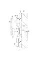
図1は本発明の第1のMPUの実装構造の好適な実施の形態を示し、図1はその構造説明図である。以下に、この第1のMPUの実装構造を説明する。
【0021】
図の第1のMPUの実装構造では、MPU10が、Cu等からなる配線回路(図示せず)が備えられたフレキシブル基板20の一方の端部の下面にフリップチップボンディング法等により実装されている。フレキシブル基板20の他方の端部の下面には、該フレキシブル基板の配線回路に接続された雄又は雌のコネクタ30が備えられている。フレキシブル基板20は、柔軟なポリイミド樹脂等から形成されていて、上下方向に容易に折曲可能な構造をしている。
【0022】
フレキシブル基板20の下方には、メモリやMPUのチップセット等を構成する半導体チップ90が上面に実装されたCu等からなる配線回路が備えられたプリント基板40が、フレキシブル基板20とほぼ平行に対向させて配置されている。プリント基板40には、MPU10を挿通可能な透孔60が設けられている。プリント基板40は、樹脂から形成されていて、リジッドな構造をしている。フレキシブル基板20に備えられた上記のコネクタ30に対向するプリント基板40の上面部分には、上記のコネクタ30に継合可能な雌又は雄のコネクタ50であって、プリント基板40の配線回路に接続されたコネクタ50が備えられている。そして、その雌雄のコネクタ30、50を介して、フレキシブル基板20とプリント基板40とが電気的に接続されている。
【0023】
フレキシブル基板20の一方の端部の下面に実装されたMPU10は、プリント基板40に設けられた透孔60を通して、その下方の電子装置の金属筐体70部分に接着剤等を用いて固定されている。金属筐体70は、Al、Al合金、Mg又はMg合金等から形成されていて、他の電子装置の筐体に再利用可能な構造をしている。
【0024】
MPU10とコネクタ30との間に位置するフレキシブル基板20部分は、金属筐体70に固定されたMPU10の上面とプリント基板40の上面側に備えられた継合された状態の雌雄のコネクタ30、50の上面との高低差に合わせて、図1に2点鎖線で示したような、平面状態から、図1に実線で示したように、緩やかな段差を持たせて上下方向に折曲されている。そして、そのフレキシブル基板20と雌雄のコネクタ30、50とを介して、MPU10がプリント基板40に電気的に接続されている。
【0025】
MPU10が固定された金属筐体70部分とは反対側の金属筐体70外側部分には、低熱伝導性の樹脂等からなる低熱伝導体80が埋設されている。そして、MPU10が発する熱が、金属筐体70を通して、低熱伝導体80が埋設された筐体外側部分に伝わりにくいように構成されている。
【0026】
図1に示した第1のMPUの実装構造は、以上のように構成されていて、この第1のMPUの実装構造においては、MPU10が固定された高熱伝導性の金属筐体70に、MPU10が発する熱を効率良く放散させることができる。
【0027】
また、MPU10が発する熱を、MPU10と低熱伝導体80との間に挟まれた金属筐体70部分を通して、金属筐体70に広く分散させて放散させることができる。そして、MPU10が固定された金属筐体70部分に、MPU10が発する熱が集中するのを防ぐことができる。それと共に、MPU10が固定された金属筐体70部分であって、MPU10が発する熱で加熱された金属筐体70部分の熱が、その金属筐体70部分側とは反対側の低熱伝導体80が埋設された筐体外側部分に伝わり難くできる。そして、その低熱伝導体80が埋設された筐体外側部分が高熱となるのを防ぐことができる。
【0028】
また、プリント基板40に設けられた透孔60の内側空間を有効利用して、プリント基板40の厚さ分、MPU10を金属筐体70内側にコンパクトに丈低く収容できる。
【0029】
また、金属筐体70に固定されたMPU10の上面と継合された状態の雌雄のコネクタ30、50の上面との高低差に合わせて、そのMPU10と雌雄のコネクタ30、50との間に位置するフレキシブル基板20部分を、上下方向に折曲させることができる。そして、そのフレキシブル基板20と雌雄のコネクタ30、50とを介して、MPU10をプリント基板40に容易かつ的確に電気的に接続できる。
【0030】
図2は本発明の第2のMPUの実装構造の好適な実施の形態を示し、図2はその構造説明図である。以下に、この第2のMPUの実装構造を説明する。
【0031】
図の第2のMPUの実装構造では、メモリやMPUのチップセット等を構成する半導体チップ90が、Cu等からなる配線回路(図示せず)が備えられた樹脂等からなるプリント基板40の下面に実装されている。プリント基板40は、リジッドな構造をしている。
【0032】
プリント基板40の下方には、Cu等からなる配線回路(図示せず)が備えられたポリイミド樹脂等からなるフレキシブル基板20が、プリント基板40とほぼ平行に対向させて配置されている。フレキシブル基板20の一方の端部の下面には、MPU10が実装されている。フレキシブル基板20の他方の端部の上面には、該フレキシブル基板の配線回路に接続された雄又は雌のコネクタ30が備えられている。
【0033】
フレキシブル基板20の他方の端部の上面に備えられた雄又は雌のコネクタ30に対向するプリント基板40の下面部分には、そのコネクタ30に継合可能な雌又は雄のコネクタ50であって、プリント基板40の配線回路に接続されたコネクタ50が備えられている。そして、その雌雄のコネクタ30、50を介して、フレキシブル基板20とプリント基板40とが電気的に接続されている。
【0034】
フレキシブル基板20に実装されたMPU10は、その下方の金属筐体70部分に接着剤等を用いて固定されている。そして、MPU10が発する熱を、金属筐体70に効率良く放散させることができるように構成されている。金属筐体70は、Al、Al合金、Mg又はMg合金等から形成されていて、他の電子装置の筐体に再利用可能な構造をしている。
【0035】
MPU10とコネクタ30との間に位置するフレキシブル基板20部分は、金属筐体70に固定されたMPU10の上面とプリント基板20の下面側に備えられた継合された状態の雌雄のコネクタ30、50の下面との高低差に合わせて、緩やかな段差を持たせて上下方向に折曲されている。そして、MPU10とプリント基板40とが、フレキシブル基板20と雌雄のコネクタ30、50とを介して、プリント基板40に電気的に接続されている。
【0036】
MPU10が固定された金属筐体70部分側とは反対側の金属筐体70外側部分には、低熱伝導性の樹脂等からなる低熱伝導体80が埋設されている。そして、MPU10が発する熱が、金属筐体70を通して、低熱伝導体80が埋設された筐体外側部分に伝わりにくいように構成されている。
【0037】
図2に示した第2のMPUの実装構造は、以上のように構成されていて、この第2のMPUの実装構造においては、MPU10が発する熱を、MPU10が固定された高熱伝導性の金属筐体70に効率良く放散させることができる。
【0038】
また、MPU10が発する熱を、MPU10と低熱伝導体80との間に挟まれた金属筐体70部分を通して、その金属筐体70部分に連なる金属筐体70に広く分散させて放散させることができる。そして、MPU10が固定された金属筐体70部分に、MPU10が発する熱が集中するのを防ぐことができる。それと共に、MPU10が固定された金属筐体70部分であって、MPU10が発する熱で加熱された金属筐体70部分の熱が、その金属筐体70部分側とは反対側の低熱伝導体80が埋設された筐体外側部分に伝わり難くできる。そして、その筐体外側部分が高熱となるのを防ぐことができる。
【0039】
また、フレキシブル基板20とプリント基板40とを電気的に接続する雌雄のコネクタ30、50が備えられたプリント基板40と金属筐体70との間の内側空間を有効利用して、その内側空間にMPU10をコンパクトに丈低く収容できる。
【0040】
また、金属筐体70に固定されたMPU10の上面とフレキシブル基板20の上面側に備えられた継合された状態の雌雄のコネクタ30、50の下面との高低差に合わせて、MPU10と雌雄のコネクタ30、50との間に位置するフレキシブル基板20部分を、上下方向に折曲させることができる。そして、そのフレキシブル基板20と雌雄のコネクタ30、50とを介して、MPU10をプリント基板40に容易かつ的確に電気的に接続できる。
【0041】
図1又は図2に示した第1又は第2のMPUの実装構造では、MPU10がベア状態でフレキシブル基板20に実装されているが、本発明の第1又は第2のMPUの実装構造においては、フレキシブル基板20にMPU10をパッケージに収納した状態で実装しても良い。その場合も、図1又は図2に示した第1又は第2のMPUの実装構造とほぼ同様な作用を持つMPUの実装構造を提供できる。
【0042】
また、図1又は図2に示した第1又は第2のMPUの実装構造は、筐体全体が高熱伝導性の金属から形成された電子装置にも利用可能である。その場合も、図1又は図2に示した第1又は第2のMPUの実装構造とほぼ同様な作用を持つMPUの実装構造を提供できる。
【0043】
【発明の効果】
以上説明したように、本発明の第1又は第2のMPUの実装構造によれば、電子装置の外側を覆うハイブリッド筐体等の高熱伝導性の金属筐体を、MPUが発する熱を放散させるヒートスプレッダに用いて、その金属筐体にMPUが発する熱を効率良く放散させることができる。
【0044】
また、MPUが発する熱を放散させるヒートスプレッダを、電子装置の金属筐体で代用して、ヒートスプレッダや放熱ファン等を電子装置のハイブリッド筐体等の金属筐体の内側空間に備える必要をなくすことができる。そして、その金属筐体の内側空間にヒートスプレッダや放熱ファン等を備えない分、電子装置の小型化、薄型化、軽量化を図れる。
【図面の簡単な説明】
【図1】本発明の第1のMPUの実装構造の概略構造説明図である。
【図2】本発明の第2のMPUの実装構造の概略構造説明図である。
【符号の説明】
10 MPU
20 フレキシブル基板
30 雄又は雌のコネクタ
40 プリント基板
50 雌又は雄のコネクタ
60 プリント基板に設けられた透孔
70 金属筐体
80 低熱伝導体
90 半導体チップ[0001]
BACKGROUND OF THE INVENTION
The present invention is, MPU (Micro of Process ing Uint substantially) for mounting in a metal housing side of the electronic device, to a mounting structure of the MPU.
[0002]
[Prior art]
The MPU has highly integrated electronic circuits formed at a high density, and the amount of heat generated during operation is several steps larger than that of a memory chip or the like.
Therefore, in the electronic device, it is necessary to efficiently dissipate the heat generated by the MPU to the outside of the MPU. It is necessary to prevent the MPU from being exposed to high heat due to heat generated by itself and malfunctioning or becoming inoperable.
[0003]
The means for efficiently radiating the heat generated by the MPU to the outside of the MPU is broadly divided into conventional ones that use a cooling fan provided near the MPU to forcibly circulate cooling air around the MPU, and the MPU. A heat spreader made of a metal with high thermal conductivity is attached to the heat spreader, and the heat spreader dissipates the heat generated by the MPU. Furthermore, the heat pipe is attached to the heat spreader attached to the MPU. There is a method of forcibly cooling the MPU through a heat spreader by the latent heat of vaporization of the refrigerant circulating inside.
[0004]
[Problems to be solved by the invention]
However, when the cooling fan, heat spreader, or heat pipe for cooling the MPU described above is provided inside the casing of the electronic device, the volume of the casing that accommodates the heat pipe increases accordingly. The electronic device with built-in cannot be reduced in size, thickness and weight.
This is particularly noticeable in electronic devices such as notebook personal computers that are required to be thinner, smaller, and lighter.
[0005]
Therefore, as a result of earnest research, the present inventor used a hybrid casing made of a combination of resin and metal in order to recycle the casing of an electronic device such as a notebook personal computer recently. It has been discovered that a highly thermally conductive metal casing made of Al, Al alloy, Mg, Mg alloy, or the like of the hybrid casing can be used as a heat spreader that dissipates the heat generated by the MPU. It was also found that if the metal casing is used for the heat spreader, the heat spreader or cooling fan for MPU cooling provided inside the casing can be eliminated, and the electronic device can be made smaller, thinner and lighter accordingly. . Then, a new MPU mounting structure was developed using a metal casing such as the hybrid casing for the heat spreader.
[0006]
That is, an object of the present invention is to provide an MPU mounting structure in which a metal casing of an electronic device is used as a heat spreader.
[0007]
[Means for Solving the Problems]
In order to achieve the above object, a first MPU mounting structure according to the present invention is an electronic device in which an MPU and a printed circuit board are provided inside a metal casing, and the lower side of the flexible circuit board on which the MPU is mounted on the lower surface. on the printed circuit board through hole is provided, are arranged substantially parallel to is opposed to the flexible substrate, the the upper surface of the lower surface and the printed circuit board of the flexible board connector is provided, via its connector The flexible board and the printed board are electrically connected, and the MPU is fixed to the metal casing portion of the electronic device below the through hole of the printed board, and is positioned between the MPU and the connector. The flexible substrate portion is configured to include an upper surface of an MPU fixed to the metal casing and an upper surface of a connector provided on the upper surface side of the printed circuit board. It is characterized by being bent in the vertical direction according to the height difference.
[0008]
In order to achieve the above object, the mounting structure of the second MPU according to the present invention is an electronic device in which an MPU and a printed board are provided inside a metal housing , and the MPU is disposed below the printed board. The flexible board mounted on the lower surface is disposed so as to face the printed circuit board substantially in parallel, and a connector is provided on the upper surface of the flexible circuit board and the lower surface of the printed circuit board. A flexible substrate is electrically connected, and the MPU is fixed to a metal casing portion of an electronic device below the flexible substrate, and the flexible substrate portion positioned between the MPU and the connector is connected to the metal casing. The upper surface of the fixed MPU and the lower surface of the connector provided on the lower surface side of the printed circuit board are bent in the vertical direction according to the height difference. It is characterized by.
[0009]
In the mounting structure of the first or second MPU, the heat generated by the MPU can be efficiently dissipated in the highly thermally conductive metal casing to which the MPU is fixed.
[0010]
In the mounting structure of the first MPU, since the MPU is fixed to the metal casing portion below the through hole provided in the printed board, the inside of the through hole provided in the printed board. By effectively using the space, the MPU can be accommodated in a compact and low-profile inside the metal casing by the thickness of the printed circuit board.
[0011]
Further, the flexible substrate portion positioned between the MPU and the connector can be bent in the vertical direction according to the height difference between the upper surface of the MPU fixed to the metal casing and the upper surface of the connector. Then, the MPU can be easily and accurately electrically connected to the printed board via the flexible board and the connector.
[0012]
In the mounting structure of the second MPU, the inner space between the printed board provided with a connector for electrically connecting the printed board and the flexible board and the metal housing is effectively used, and the inner space is provided. The MPU can be accommodated in a compact and low length.
[0013]
In addition, the flexible substrate portion positioned between the MPU and the connector can be bent in the vertical direction according to the height difference between the upper surface of the MPU fixed to the metal housing and the lower surface of the connector. Then, the MPU can be easily and accurately electrically connected to the printed board via the flexible board and the connector.
[0014]
In the mounting structure of the first or second MPU of the present invention, a low thermal conductor is embedded in a metal casing outer side opposite to the metal casing part side to which the MPU is fixed. Is suitable.
[0015]
In the mounting structure of the first or second MPU, the heat generated by the MPU is a metal casing portion to which the MPU is fixed, and the metal casing sandwiched between the MPU and the low thermal conductor. Through the body part, it can be widely dispersed and dissipated in the metal casing connected to the metal casing part. And it can prevent that the heat which MPU emits concentrates on the metal case part to which MPU was joined. At the same time, the metal casing part to which the MPU is fixed and the heat of the metal casing part heated by the heat generated by the MPU is embedded in the outer part of the metal casing opposite to the metal casing part side. It is difficult to be transmitted to the low heat conductor. And it can prevent that the housing | casing outer side part with which the low heat conductor was embed | buried becomes high temperature, and can prevent a person who touched the hand to the housing | casing outer part suffering a burn etc.
[0016]
In the mounting structure of the 1st or 2nd MPU of this invention, it is suitable for the said flexible substrate to consist of polyimide resins.
[0017]
In the mounting structure of the first or second MPU, a flexible substrate that can be easily bent in the vertical direction can be formed using a flexible polyimide resin.
[0018]
In the first or second MPU mounting structure of the present invention, it is preferable that the metal housing to which the MPU is fixed is made of Al, Al alloy, Mg, or Mg alloy.
[0019]
In the mounting structure of the first or second MPU, the heat generated by the MPU can be efficiently dissipated in the highly thermally conductive metal casing made of Al, Al alloy, Mg or Mg alloy. In addition, the metal casing made of Al, Al alloy, Mg, or Mg alloy can be reused in a casing of another electronic device by remelting the metal casing.
[0020]
DETAILED DESCRIPTION OF THE INVENTION
Next, embodiments of the present invention will be described with reference to the drawings.
FIG. 1 shows a preferred embodiment of the first MPU mounting structure of the present invention, and FIG. 1 is an explanatory diagram of the structure. Hereinafter, the mounting structure of the first MPU will be described.
[0021]
In the first MPU mounting structure shown in the figure, the
[0022]
Below the
[0023]
The
[0024]
The portion of the
[0025]
A low
[0026]
The first MPU mounting structure shown in FIG. 1 is configured as described above. In the first MPU mounting structure, the
[0027]
Further, the heat generated by the
[0028]
Further, by effectively using the inner space of the through
[0029]
In addition, according to the height difference between the upper surface of the male and
[0030]
FIG. 2 shows a preferred embodiment of the second MPU mounting structure of the present invention, and FIG. 2 is an explanatory diagram of the structure. Hereinafter, the mounting structure of the second MPU will be described.
[0031]
In the mounting structure of the second MPU in the figure, the lower surface of the printed
[0032]
Below the printed
[0033]
The lower surface portion of the printed
[0034]
The
[0035]
The portion of the
[0036]
A low
[0037]
The second MPU mounting structure shown in FIG. 2 is configured as described above. In the second MPU mounting structure, the heat generated by the
[0038]
Further, the heat generated by the
[0039]
Further, the inner space between the printed
[0040]
Further, according to the height difference between the upper surface of the
[0041]
In the first or second MPU mounting structure shown in FIG. 1 or FIG. 2, the
[0042]
The mounting structure of the first or second MPU shown in FIG. 1 or FIG. 2 can also be used for an electronic device in which the entire casing is made of a metal having high thermal conductivity. Even in that case, it is possible to provide an MPU mounting structure having substantially the same operation as the first or second MPU mounting structure shown in FIG. 1 or FIG.
[0043]
【The invention's effect】
As described above, according to the first or second MPU mounting structure of the present invention, the heat generated by the MPU is dissipated in the highly thermally conductive metal casing such as a hybrid casing that covers the outside of the electronic device. By using the heat spreader, the heat generated by the MPU can be efficiently dissipated in the metal casing.
[0044]
In addition, the heat spreader that dissipates the heat generated by the MPU may be replaced with the metal casing of the electronic device, eliminating the need to provide a heat spreader, a heat dissipation fan, or the like in the inner space of the metal casing such as the hybrid casing of the electronic device. it can. Further, the electronic device can be reduced in size, thickness, and weight because the heat spreader and the heat radiating fan are not provided in the inner space of the metal casing.
[Brief description of the drawings]
FIG. 1 is a schematic structural explanatory diagram of a mounting structure of a first MPU of the present invention.
FIG. 2 is a schematic structural explanatory diagram of a second MPU mounting structure according to the present invention.
[Explanation of symbols]
10 MPU
DESCRIPTION OF
Claims (5)
前記MPUが下面に実装されたフレキシブル基板の下方に、透孔が設けられた前記プリント基板が、フレキシブル基板とほぼ平行に対向させて配置され、そのフレキシブル基板の下面とプリント基板の上面とには、コネクタが備えられて、そのコネクタを介して前記フレキシブル基板とプリント基板とが電気的に接続され、前記MPUが、前記プリント基板の透孔を通して、その下方の電子装置の金属筐体部分に固定されると共に、MPUとコネクタとの間に位置する前記フレキシブル基板部分が、前記金属筐体に固定されたMPUの上面と前記プリント基板の上面側に備えられたコネクタの上面との高低差に合わせて、上下方向に折曲されてなることを特徴とするMPUの実装構造。 In an electronic device in which an MPU and a printed circuit board are provided inside a metal housing,
The printed circuit board provided with a through hole is disposed below the flexible board on which the MPU is mounted on the lower surface so as to face the flexible board substantially parallel to the lower surface of the flexible board and the upper surface of the printed circuit board. The flexible board and the printed board are electrically connected via the connector, and the MPU is fixed to the metal casing portion of the electronic device below the through hole of the printed board. In addition, the flexible board portion located between the MPU and the connector is adapted to the height difference between the upper face of the MPU fixed to the metal casing and the upper face of the connector provided on the upper face side of the printed board. An MPU mounting structure characterized by being bent in the vertical direction.
前記プリント基板の下方に、前記MPUが下面に実装されたフレキシブル基板が、プリント基板とほぼ平行に対向させて配置され、そのフレキシブル基板の上面とプリント基板の下面とには、コネクタが備えられて、そのコネクタを介して前記プリント基板とフレキシブル基板とが電気的に接続され、前記MPUが、その下方の電子装置の金属筐体部分に固定されると共に、MPUとコネクタとの間に位置する前記フレキシブル基板部分が、前記金属筐体に固定されたMPUの上面と前記プリント基板の下面側に備えられたコネクタの下面との高低差に合わせて、上下方向に折曲されてなることを特徴とするMPUの実装構造。 In an electronic device in which an MPU and a printed circuit board are provided inside a metal housing,
Below the printed circuit board, a flexible board on which the MPU is mounted on the lower surface is disposed substantially parallel to is opposed to the printed board, the the lower surface of the upper surface and the printed circuit board of the flexible board connector is provided The printed board and the flexible board are electrically connected via the connector, and the MPU is fixed to the metal casing portion of the electronic device below the MPU and the connector. The flexible board portion is bent in the vertical direction according to the height difference between the upper surface of the MPU fixed to the metal casing and the lower surface of the connector provided on the lower surface side of the printed board. MPU mounting structure.
Priority Applications (1)
| Application Number | Priority Date | Filing Date | Title |
|---|---|---|---|
| JP14742999A JP3661489B2 (en) | 1999-05-27 | 1999-05-27 | MPU mounting structure |
Applications Claiming Priority (1)
| Application Number | Priority Date | Filing Date | Title |
|---|---|---|---|
| JP14742999A JP3661489B2 (en) | 1999-05-27 | 1999-05-27 | MPU mounting structure |
Publications (2)
| Publication Number | Publication Date |
|---|---|
| JP2000340735A JP2000340735A (en) | 2000-12-08 |
| JP3661489B2 true JP3661489B2 (en) | 2005-06-15 |
Family
ID=15430128
Family Applications (1)
| Application Number | Title | Priority Date | Filing Date |
|---|---|---|---|
| JP14742999A Expired - Fee Related JP3661489B2 (en) | 1999-05-27 | 1999-05-27 | MPU mounting structure |
Country Status (1)
| Country | Link |
|---|---|
| JP (1) | JP3661489B2 (en) |
Families Citing this family (1)
| Publication number | Priority date | Publication date | Assignee | Title |
|---|---|---|---|---|
| US10276487B1 (en) * | 2017-10-18 | 2019-04-30 | Micron Technology, Inc. | Semiconductor device with flexible circuit for enabling non-destructive attaching and detaching of device to system board |
-
1999
- 1999-05-27 JP JP14742999A patent/JP3661489B2/en not_active Expired - Fee Related
Also Published As
| Publication number | Publication date |
|---|---|
| JP2000340735A (en) | 2000-12-08 |
Similar Documents
| Publication | Publication Date | Title |
|---|---|---|
| US6219243B1 (en) | Heat spreader structures for enhanced heat removal from both sides of chip-on-flex packaged units | |
| JP3294785B2 (en) | Heat dissipation structure of circuit element | |
| US6712621B2 (en) | Thermally enhanced interposer and method | |
| US5933324A (en) | Apparatus for dissipating heat from a conductive layer in a circuit board | |
| US5513070A (en) | Dissipation of heat through keyboard using a heat pipe | |
| JP3147087B2 (en) | Stacked semiconductor device heat dissipation structure | |
| US5804875A (en) | Computer system with heat sink having an integrated grounding tab | |
| JP3281220B2 (en) | Circuit module cooling system | |
| JP3813281B2 (en) | Electronic device having IC card slot | |
| JP2008140924A (en) | Electronic device | |
| JPH10270884A (en) | Heat dissipating structure for plug-in unit | |
| TWM377062U (en) | Electronic device with a heat insulating structure | |
| JPH09213851A (en) | Heat radiation method and heat radiation means for ic device | |
| JPH06169189A (en) | Chip type heat generating component and packaging thereof | |
| JP5115200B2 (en) | Electronic device, package having the same, and electronic device | |
| JP3661489B2 (en) | MPU mounting structure | |
| JPH11163476A (en) | Heat-radiation structure of circuit board and power source control device | |
| JPH07106721A (en) | Printed circuit board and heat radiating method | |
| JP3378174B2 (en) | Heat dissipation structure of high heating element | |
| JP3068488B2 (en) | Printed board | |
| JPH1098287A (en) | Cooler for circuit board module and portable electronic equipment having the cooler | |
| US6399877B1 (en) | Heat sink | |
| JPH11186771A (en) | Circuit module and information processing device | |
| JP3295299B2 (en) | Heat dissipation structure of card-shaped electronic components | |
| JP2912268B2 (en) | Method and apparatus for radiating electronic components |
Legal Events
| Date | Code | Title | Description |
|---|---|---|---|
| A131 | Notification of reasons for refusal |
Free format text: JAPANESE INTERMEDIATE CODE: A131 Effective date: 20041210 |
|
| A521 | Request for written amendment filed |
Free format text: JAPANESE INTERMEDIATE CODE: A523 Effective date: 20050127 |
|
| TRDD | Decision of grant or rejection written | ||
| A01 | Written decision to grant a patent or to grant a registration (utility model) |
Free format text: JAPANESE INTERMEDIATE CODE: A01 Effective date: 20050314 |
|
| A61 | First payment of annual fees (during grant procedure) |
Free format text: JAPANESE INTERMEDIATE CODE: A61 Effective date: 20050314 |
|
| R150 | Certificate of patent or registration of utility model |
Free format text: JAPANESE INTERMEDIATE CODE: R150 |
|
| FPAY | Renewal fee payment (event date is renewal date of database) |
Free format text: PAYMENT UNTIL: 20090401 Year of fee payment: 4 |
|
| FPAY | Renewal fee payment (event date is renewal date of database) |
Free format text: PAYMENT UNTIL: 20100401 Year of fee payment: 5 |
|
| FPAY | Renewal fee payment (event date is renewal date of database) |
Free format text: PAYMENT UNTIL: 20110401 Year of fee payment: 6 |
|
| FPAY | Renewal fee payment (event date is renewal date of database) |
Free format text: PAYMENT UNTIL: 20120401 Year of fee payment: 7 |
|
| FPAY | Renewal fee payment (event date is renewal date of database) |
Free format text: PAYMENT UNTIL: 20130401 Year of fee payment: 8 |
|
| FPAY | Renewal fee payment (event date is renewal date of database) |
Free format text: PAYMENT UNTIL: 20130401 Year of fee payment: 8 |
|
| FPAY | Renewal fee payment (event date is renewal date of database) |
Free format text: PAYMENT UNTIL: 20140401 Year of fee payment: 9 |
|
| LAPS | Cancellation because of no payment of annual fees |