JP3636148B2 - Display driver, electro-optical device, and display driver parameter setting method - Google Patents
Display driver, electro-optical device, and display driver parameter setting method Download PDFInfo
- Publication number
- JP3636148B2 JP3636148B2 JP2002061468A JP2002061468A JP3636148B2 JP 3636148 B2 JP3636148 B2 JP 3636148B2 JP 2002061468 A JP2002061468 A JP 2002061468A JP 2002061468 A JP2002061468 A JP 2002061468A JP 3636148 B2 JP3636148 B2 JP 3636148B2
- Authority
- JP
- Japan
- Prior art keywords
- display
- register
- control
- display driver
- refresh
- Prior art date
- Legal status (The legal status is an assumption and is not a legal conclusion. Google has not performed a legal analysis and makes no representation as to the accuracy of the status listed.)
- Expired - Lifetime
Links
Images


Classifications
-
- G—PHYSICS
- G09—EDUCATION; CRYPTOGRAPHY; DISPLAY; ADVERTISING; SEALS
- G09G—ARRANGEMENTS OR CIRCUITS FOR CONTROL OF INDICATING DEVICES USING STATIC MEANS TO PRESENT VARIABLE INFORMATION
- G09G3/00—Control arrangements or circuits, of interest only in connection with visual indicators other than cathode-ray tubes
- G09G3/20—Control arrangements or circuits, of interest only in connection with visual indicators other than cathode-ray tubes for presentation of an assembly of a number of characters, e.g. a page, by composing the assembly by combination of individual elements arranged in a matrix no fixed position being assigned to or needed to be assigned to the individual characters or partial characters
-
- G—PHYSICS
- G09—EDUCATION; CRYPTOGRAPHY; DISPLAY; ADVERTISING; SEALS
- G09G—ARRANGEMENTS OR CIRCUITS FOR CONTROL OF INDICATING DEVICES USING STATIC MEANS TO PRESENT VARIABLE INFORMATION
- G09G2320/00—Control of display operating conditions
- G09G2320/06—Adjustment of display parameters
- G09G2320/066—Adjustment of display parameters for control of contrast
Landscapes
- Engineering & Computer Science (AREA)
- Physics & Mathematics (AREA)
- Computer Hardware Design (AREA)
- General Physics & Mathematics (AREA)
- Theoretical Computer Science (AREA)
- Control Of Indicators Other Than Cathode Ray Tubes (AREA)
- Liquid Crystal (AREA)
- Liquid Crystal Display Device Control (AREA)
Description
【0001】
【発明の属する技術分野】
本発明は、表示ドライバ、電気光学装置、及び表示ドライバのパラメータ設定方法に関する。
【0002】
【背景技術及び発明が解決しようとする課題】
携帯電話などの電子機器に用いられる液晶装置(広義には電気光学装置)では、最適な表示特性で表示動作を行うことが望まれている。
【0003】
ところが、液晶装置の表示パネルには表示特性のバラツキがあるため、このバラツキの影響を如何にして抑えるかが重要な技術的課題となる。
【0004】
また、液晶装置の表示特性は、静電気(ESD)などの外部的な要因が発生した場合にも、最適に維持されることが望まれる。
【0005】
また、液晶装置が組み込まれる電子機器では、電子機器のファームウェアが、液晶装置の表示動作を制御する。この場合に、電子機器の開発期間の短縮化のためには、ファームウェアの作成作業を、なるべく簡素化できることが望まれる。
【0006】
本発明は以上のような課題に鑑みてなされたものであり、その目的とするところは、適正な表示特性を実現できる表示ドライバ、電気光学装置、及び表示ドライバのパラメータ設定方法を提供することにある。
【0007】
【課題を解決するための手段】
本発明は、表示パネルを駆動するための表示ドライバであって、表示ドライバを制御するための制御レジスタと、表示ドライバの外部又は内部に設けられ表示特性制御パラメータを少なくとも記憶するメモリに対して、アクセス制御を行うメモリ制御回路と、所与のリフレッシュタイミングで、前記メモリから読み出された表示特性制御パラメータを前記制御レジスタに書き込み、前記制御レジスタのリフレッシュ処理を行うレジスタ書き込み回路とを含む表示ドライバに関係する。
【0008】
本発明によれば、所与のリフレッシュタイミングで、メモリから読み出された表示特性制御パラメータが制御レジスタに書き込まれ、制御レジスタのリフレッシュ処理が行われる。従って、適正な表示特性制御パラメータを用いて表示パネルの表示制御を行うことが可能になり、適正な表示特性を安定して維持することが可能になる。
【0009】
また本発明では、前記レジスタ書き込み回路が、表示パネルの非表示期間において、表示特性制御パラメータを前記制御レジスタに書き込み、前記制御レジスタのリフレッシュ処理を行うようにしてもよい。
【0010】
この場合、非表示期間は、例えば、制御レジスタへの書き込み処理が、表示パネルの表示動作に悪影響を与えない期間である。但し、非表示期間以外の期間において、リフレッシュ処理を行うことも可能である。
【0011】
また本発明では、前記レジスタ書き込み回路が、電源投入後又はシステムリセット後に、定期的に、表示特性制御パラメータを前記制御レジスタに書き込み、前記制御レジスタのリフレッシュ処理を行うようにしてもよい。
【0012】
なお、定期的に発生する非表示期間において、リフレッシュ処理を行うことが更に望ましい。
【0013】
また本発明では、前記メモリが、前記レジスタ書き込み回路により行われるリフレッシュ処理の期間情報を記憶し、前記レジスタ書き込み回路が、前記メモリから読み出された期間情報を、前記制御レジスタに書き込むようにしてもよい。
【0014】
また本発明では、前記レジスタ書き込み回路が、電源投入時又はシステムリセット時に、前記メモリから読み出された表示特性制御パラメータを前記制御レジスタに書き込み、前記制御レジスタのイニシャライズ処理を行うようにしてもよい。
【0015】
また本発明は、表示パネルを駆動するための表示ドライバであって、表示ドライバを制御するための制御レジスタと、表示ドライバの外部又は内部に設けられ表示特性制御パラメータを少なくとも記憶するメモリに対して、アクセス制御を行うメモリ制御回路と、電源投入時又はシステムリセット時に、前記メモリから読み出された表示特性制御パラメータを前記制御レジスタに書き込み、前記制御レジスタのイニシャライズ処理を行うレジスタ書き込み回路とを含む表示ドライバに関係する。
【0016】
本発明によれば、電源投入時又はシステムリセット時に、メモリから読み出された表示特性制御パラメータが制御レジスタに書き込まれ、制御レジスタのイニシャライズ処理が行われる。従って本発明によれば、適正な表示特性制御パラメータを自動的に読み込んで、表示パネルの表示制御を行うことが可能になる。
【0017】
また本発明では、前記制御レジスタが、表示特性制御パラメータを記憶し処理部によりアクセス可能な第1のレジスタ群と、処理部によりアクセス可能な第2のレジスタ群を含むようにしてもよい。
【0018】
この場合に、第2のレジスタ群には、表示制御パラメータ以外の情報(例えば表示に関する各種のコマンド情報)を記憶させることができる。
【0019】
また本発明では、前記レジスタ書き込み回路が、前記第1のレジスタ群に表示特性制御パラメータを書き込んでいる際には、該第1のレジスタ群への処理部のアクセスを禁止するようにしてもよい。
【0020】
このようにすれば、処理部からのアクセスとメモリからのアクセスが衝突する事態を防止できる。
【0021】
また本発明では、前記メモリが、表示ドライバ又は表示パネルの製造情報を記憶し、前記レジスタ書き込み回路が、前記メモリから読み出された製造情報を、前記制御レジスタに書き込むようにしてもよい。
【0022】
この場合、製造情報としては、例えば、製造識別情報、製品バージョン情報、或いは製品特定情報などを含ませることができる。
【0023】
また本発明では、前記表示特性制御パラメータが、コントラスト調整パラメータ、表示制御パラメータ、及び階調制御パラメータの少なくとも1つを含むようにしてもよい。
【0024】
但し、表示特性制御パラメータとして、これ以外のパラメータを含ませることも可能である。
【0025】
また本発明では、前記表示特性制御パラメータが、表示パネル毎に又は表示パネルの機種毎にその値が異なるパラメータであってもよい。
【0026】
また本発明の電気光学装置は、上記のいずれか記載の表示ドライバと、前記表示ドライバにより駆動される表示パネルと、前記表示ドライバの動作を制御する処理部とを含む電気光学装置に関係する。
【0027】
また本発明は、上記のいずれか記載の表示ドライバのパラメータ設定方法であって、表示ドライバにより駆動される表示パネルの表示特性を測定し、測定により特定される表示特性制御パラメータを、前記メモリに書き込むパラメータ設定方法に関係する。
【0028】
【発明の実施の形態】
以下、本発明の好適な実施の形態について図面を用いて詳細に説明する。なお、以下に説明する実施の形態は、特許請求の範囲に記載された本発明の内容を不当に限定するものではない。また以下で説明される構成の全てが本発明の必須構成要件であるとは限らない。
【0029】
1.電気光学装置
図1に、本実施形態の電気光学装置の構成例を示す。
【0030】
この電気光学装置(狭義には液晶装置)は、表示パネル100(狭義には液晶パネル)を含む。
【0031】
この表示パネル100は、複数のデータ線(信号線)と、複数の走査線と、データ線及び走査線により特定される複数の画素を有する。そして、各画素領域における電気光学素子(狭義には、液晶素子)の光学特性を変化させることで、表示動作を実現する。
【0032】
なお、表示パネル100は、単純マトリクス方式のパネルであってもよいし、薄膜トランジスタ(Thin Film Transistor:TFT)や薄膜ダイオード(Thin Film Diode:TFD)などのスイッチング素子(2端子型非線形素子)を用いたアクティブマトリクス方式のパネルであってもよい。
【0033】
また電気光学装置は、データ線ドライバ110(データ線駆動回路、Xドライバ、ソースドライバ)と、走査線ドライバ120、122(走査線駆動回路、Yドライバ、ゲートドライバ)を含む。
【0034】
ここでデータ線ドライバ110は、画像データに基づいて表示パネル100のデータ線を駆動する。一方、走査線ドライバ120、122は、表示パネル100の走査線を順次走査駆動する。
【0035】
なお、走査線ドライバ120、122を、データ線ドライバ110に内蔵させてもよい。
【0036】
また電気光学装置は、MPU130(広義には処理部)を含む。
【0037】
ここで、MPU(Micro Processor Unit)130は、データ線ドライバ110、走査線ドライバ120、122、電源回路132、EEPROM134の制御等を行う。
【0038】
より具体的には、MPU130は、データ線ドライバ110及び走査線ドライバ120、122に対しては、動作モードの設定や垂直同期信号や水平同期信号の供給を行う。また、電源回路132に対しては、電源設定についての指示を行う。また、EEPROM134に対しては、例えばデータ線ドライバ110を介して、メモリへのアクセス指示などを行う。
【0039】
なお、MPU130(処理部)は、汎用プロセッサ(CPU)により実現してもよいし、ASICであるコントローラ回路により実現してもよい。
【0040】
また、MPU130の機能を、電子機器(携帯電話、ページャ、時計、液晶テレビ、カーナビゲーション装置、電卓、ワードプロセッサ、プロジェクタ又はPOS端末等)が有する外部のMPU(処理部)により実現してもよい。
【0041】
電源回路132は、外部から供給される基準電圧に基づいて、表示パネル100の駆動に必要な各種の電源電圧(階調電圧)を生成する。そして、生成された電源電圧を、データ線ドライバ110や走査線ドライバ120、122に供給する。
【0042】
EEPROM134(広義にはメモリ、不揮発性メモリ或いはROM)は、電気光学装置を動作させるための種々の情報を記憶する。
【0043】
より具体的には、本実施形態のEEPROM134は、表示特性制御パラメータ(コントラスト調整パラメータ、表示制御パラメータ又は階調制御パラメータ等)を記憶する。そして、この記憶された表示特性制御パラメータは、例えば、電源投入時や、システムリセット時や、リフレッシュタイミング時に読み出される。そして、読み出された表示特性制御パラメータは、データ線ドライバ110が有する制御レジスタに格納される。
【0044】
なお、EEPROM134は、データ線ドライバ110の外部に設けてもよいし、内部に設けてもよい。また、データ線ドライバ110を介さずに、MPU130が直接にEEPROM134にアクセスするようにしてもよい。
【0045】
また、データ線ドライバ110、走査線ドライバ120、122、MPU130、電源回路132、EEPROM134の一部又は全部を、表示パネル100(ガラス基板)上に形成してもよい。
【0046】
2.データ線ドライバ
図2に、本実施形態のデータ線ドライバ110(広義には表示ドライバ或いは表示駆動回路)の構成例を示す。なお、本実施形態のデータ線ドライバ110は図2に示す全ての回路ブロックを含む必要はなく、その一部を省略してもよい。
【0047】
MPUインターフェース500には、反転チップセレクト信号XCS、コマンド/データの識別信号A0、反転リード信号XRD、反転ライト信号XWR、反転リセット信号XRESなどが入力される。
【0048】
入出力バッファ502には、例えば8ビットのデータ(コマンド)D7〜D0が入力される。
【0049】
バスホルダ512は、内部バス510上のデータを一時的に保持するためのものである。
【0050】
コマンドデコーダ514は、MPUインターフェース500を介してMPU130から入力されたコマンドをデコード(解読)し、デコード結果をMPU側制御回路530等に伝える。
【0051】
ステータスレジスタ516は、データ線ドライバ110のステータス情報(例えば表示がオン状態か否か、パーシャル表示モードか否か、スリープモードか否か等)を保持する。
【0052】
MPU側制御回路530は、コマンドデコーダ514を介して入力されるMPU130のコマンドに基づいて、表示データRAM560に対するリード・ライト動作を制御する。このリード・ライト動作は、MPU側制御回路530により制御されるカラムアドレス制御回路540及びページアドレス制御回路550により実現される。
【0053】
カラムアドレス制御回路540は、表示データの書き込みカラムアドレスと読み出しカラムアドレスを指定する。
【0054】
ページアドレス制御回路550は、表示データの書き込みページアドレスと表示データの読み出しページアドレスとを指定する。また、ページアドレス制御回路550は、ドライバ側制御回路570により制御されて1ライン毎に表示アドレスを指定する。
【0055】
ドライバ側制御回路570(パネル側制御回路)は、発振回路576からの発振出力に基づいて、階調制御パルスGCP(パルス幅刻み用のクロックパルス信号)、極性反転信号FR、ラッチパルスLPなどを発生し、ページアドレス制御回路550、PWMデコーダ回路580などを制御する。
【0056】
PWMデコーダ回路580は、表示データRAM560から読み出された表示データに基づいて、PWM(パルス幅変調)のデコード処理を行う。
【0057】
駆動回路600は、PWMデコーダ回路580からの信号を、表示パネル系の電圧に応じた電圧にシフトさせ、表示パネル100のデータ線に供給する。
【0058】
以上のような構成により本実施形態では、表示パネル100に種々の画像を表示できる。
【0059】
3.表示特性制御パラメータのイニシャライズ及びリフレッシュ
さて、携帯電話などの電子機器に用いられる液晶装置(電気光学装置)では、その検査時・出荷時に、表示パネルの表示特性(コントラスト、色合い等)の調整を行うことが望ましい。そして、最適な調整が行われた後に、電子機器のメーカに出荷し、電子機器に組み込むことが望ましい。
【0060】
この場合に、電気機器のメーカにとっては、表示パネルの表示特性は最適なものでありさえすればよく、表示特性の設定内容については興味がない。そして、このような表示特性の設定を、ファームウェアに行わせるようにすると、表示パネル毎に或いは表示パネルの機種毎に、ファームウェアにおける表示特性設定の記述部分を変更しなければならなくなる。このため、電気機器のメーカに無用で煩雑な作業を強いる可能性がある。
【0061】
また、携帯電話などの電子機器では、その使用状況により、静電気(ESD)などの種々の外部要因が発生する。そして、設定された表示特性が、この外部要因が原因となって変更されてしまうと、最適な表示特性を維持できなくなる可能性がある。
【0062】
そこで本実施形態では、以下に説明するような構成を採用することで、上述の種々の問題点を解決している。
【0063】
即ち、本実施形態のデータ線ドライバ110では図2に示すように、メモリ制御回路579を設けている。
【0064】
このメモリ制御回路579は、図1のEEPROM134に対するアクセス制御(リード・ライト制御)を行う。
【0065】
より具体的には、EEPROM134には、表示パネル100の表示特性(コントラスト、色合い等)を制御(設定)するためのパラメータが記憶されている。この表示特性制御パラメータは、例えば、液晶装置(電子機器)の出荷時・検査時に、表示パネル100の表示特性を測定することで得ることができ、測定結果に応じた最適な表示特性制御パラメータが、EEPROM134に書き込まれる。この表示特性制御パラメータを用いることで、表示パネル100の表示特性のバラツキを吸収し、表示パネル毎に又は表示パネルの機種毎に表示特性が異なってしまう事態を防止できる。本実施形態のメモリ制御回路579は、この表示特性制御パラメータなどを含む種々の情報をEEPROM134から読み出す。
【0066】
また本実施形態のデータ線ドライバ110では、MPU側制御回路530に、レジスタ書き込み回路20(レジスタ・リフレッシュ回路、レジスタ・イニシャライズ回路)、制御レジスタ30、演算回路50を含ませている。
【0067】
ここで制御レジスタ30は、データ線ドライバ110の制御に使用されるレジスタである。
【0068】
より具体的には、図1のMPU130がコマンドを発行すると、このコマンドは図2のコマンドデコーダ514によりデコードされる。そして、そのコマンドにより設定されるパラメータが、入出力バッファ502及びレジスタ書き込み回路20を介して、制御レジスタ30に書き込まれる。これにより、MPU側制御回路530は、制御レジスタ30に書き込まれた制御パラメータ(動作パラメータ、コマンドパラメータ)に基づいて動作するようになる。即ち、MPU側制御回路530は、制御レジスタ30の内容に基づいて、カラムアドレス制御回路540、I/Oバッファ542、ページアドレス制御回路550、ドライバ側制御回路570などを制御する。
【0069】
このような制御レジスタ30を設けることで、MPU130は、自身が発行したコマンドに従ってデータ線ドライバ110を動作させ、表示パネル100を表示制御できるようになる。
【0070】
なお、制御レジスタ30は、Dフリップフロップなどの保持回路で実現してもよいし、RAMなどのメモリにより実現してもよい。
【0071】
本実施形態では、レジスタ書き込み回路20が、この制御レジスタ30への書き込み処理を行う。
【0072】
より具体的には、レジスタ書き込み回路20は、電源投入時又はシステムリセット時(イニシャライズ時)に、図1のEEPROM134(メモリ、不揮発性メモリ或いはROM)から読み出された表示特性制御パラメータ(動作パラメータ、コマンドパラメータ)を制御レジスタ30に書き込み、制御レジスタ30のイニシャライズ処理を行う。
【0073】
このようなイニシャライズ処理を行うことで、電源投入時やシステムリセット時(ソフトウェアリセット時)に、EEPROM134に記憶される表示特性制御パラメータが、制御レジスタ30に自動的に書き込まれるようになる。
【0074】
従って、MPU側制御回路530は、制御レジスタ30に書き込まれた表示特性制御パラメータを用いて、表示パネル100の最適な表示制御を行うことができる。
【0075】
また、MPU130(処理部)上で動作するファームウェア(プログラム)は、電源投入時やシステムリセット時に、表示特性制御パラメータを制御レジスタ30に書き込む必要が無くなる。これにより、表示特性制御パラメータをファームウェアに記述しなくても済むようになり、ファームウェアの作成作業を簡素化できる。また、表示パネルの機種が異なっても、同じファームウェアを使用できるようになり、電子機器メーカ等の開発負担を軽減できる。
【0076】
また本実施形態では、レジスタ書き込み回路20が、所与のリフレッシュタイミングで、EEPROM134から読み出された表示特性制御パラメータ(動作パラメータ、コマンドパラメータ)を制御レジスタ30に書き込み、制御レジスタ30のリフレッシュ処理を行う。
【0077】
このようにすることで、表示パネル100の表示特性を常に最適に維持できるようになる。
【0078】
即ち、携帯電話などの電子機器では、その使用状況により、静電気などの外部要因が原因となって、制御レジスタ30の表示特性制御パラメータが、不適正な値に書き換えられたり、消失してしまう可能性がある。そして、表示特性制御パラメータが書き換えられたり、消失すると、最適な表示特性を維持できなくなる。
【0079】
本実施形態では、このような場合にも、レジスタ書き込み回路20がリフレッシュ動作を行うことで、EEPROM134に記憶される最適な表示特性制御パラメータが、制御レジスタ30に再度書き込まれる。従って、静電気などの外部要因が発生しても、表示パネル100の表示特性を最適に維持できる。
【0080】
また、本実施形態では、コントラスト調整処理を簡素化するために、制御レジスタ30に補正パラメータレジスタ40(VOLDEF)を含ませると共に、演算回路50を設けている。
【0081】
ここで、補正パラメータレジスタ40は、コントラスト調整(設定)値を補正するための補正パラメータ(表示特性制御パラメータの1つ)を記憶するレジスタである。この補正パラメータは、例えば、液晶装置(電子機器)の出荷時・検査時に、表示パネル100のコントラスト(明るさ)などを測定することで得ることができ、測定結果に応じた最適な補正パラメータが、EEPROM134に書き込まれる。この補正パラメータを用いることで、表示パネル100のコントラストのバラツキを吸収し、表示パネル毎に又は表示パネルの機種毎に表示特性が異なってしまう事態を防止できる。
【0082】
そして、本実施形態では、EEPROM134に記憶されたこの補正パラメータが、メモリ制御回路579、レジスタ書き込み回路20を介して、補正パラメータレジスタ40に書き込まれる。より具体的には、電源投入時又はシステムリセット時に、補正パラメータがレジスタ40に書き込まれ、レジスタ40のイニシャライズ処理が行われる。また、所与のリフレッシュタイミングで、補正パラメータがレジスタ40に書き込まれ、レジスタ40のリフレッシュ処理が行われるようになる。
【0083】
図2の演算回路50は、MPU130(処理部)により指示されるコントラスト調整値に対して、補正パラメータにより特定される補正値を加算し、補正コントラスト調整値を演算する回路である。
【0084】
即ち本実施形態では、MPU130がコマンド等を発行することでコントラスト調整値を設定する。すると、演算回路50は、この設定されたコントラスト調整値に対して、レジスタ40の補正パラメータにより特定される補正値を加算し、補正コントラスト調整値を求める。そして、この補正コントラスト調整値は、例えば電源制御回路578を介して図1の電源回路132に出力される。
【0085】
すると、電源回路132は、この補正コントラスト調整値に応じた電源電圧を生成し、データ線ドライバ110(駆動回路600)や走査線ドライバ120、122に供給する。これにより、表示パネル100は、補正コントラスト調整値に応じたコントラスト(明るさ)で表示動作を行うようになる。
【0086】
4.リフレッシュタイミング
本実施形態では、表示パネル100(表示ドライバ)の非表示期間において、制御レジスタ30のリフレッシュ処理を行っている。
【0087】
より具体的には本実施形態では図3(A)に示すように、表示パネル100に、表示ライン領域DRGとオフライン(display off line)領域FRG1、FRG2が設けられている。
【0088】
ここで表示ライン領域DRGは、実際に画像が表示される領域である。一方、オフライン領域FRG1、FRG2は、画像が表示されない領域(ダミー領域)である。
【0089】
例えば、上側のオフライン領域FRG1が存在しない場合を想定する。この場合には、表示ライン領域DRGの一番上側の第1の走査ラインでは、その下側には第2の走査ラインが存在するが、その上側には走査ラインが存在しなくなる。一方、第2の走査ラインでは、その下側に第3の走査ラインが存在すると共に、その上側にも第1の走査ラインが存在する。従って、オフライン領域FRG1が存在しない場合には、第1の走査ラインと第2の走査ラインとで、寄生する容量等が異なってしまい、その部分の表示状態にむら等が生じてしまう。
【0090】
これに対して、図3(A)に示すようなオフライン領域FRG1を設ければ、第1の走査ラインの上にも、ダミーの走査ラインが存在するようになる。この結果、第1、第2の走査ラインの寄生容量等をほぼ同一にでき、表示状態にむらが生じるのを防止できる。
【0091】
同様に、下側のオフライン領域FRG2を設ければ、表示ライン領域DRGの一番下側の第Nの走査ラインと、その上側の第N−1の走査ラインとで、寄生容量等をほぼ同一にでき、表示状態にむらが生じるのを防止できる。
【0092】
また、オフライン領域FRG1、FRG2は、例えば次のような目的のために設けられる。
【0093】
即ち、表示パネル100の表示ライン数(表示ライン領域DRGのライン数)は、電子機器の機種毎に異なった本数になるのが一般的である。
【0094】
この場合に、電子機器の機種毎に、異なった表示ライン数の表示パネル100を使用すると、製品コストの増加、設計期間の長期化等の問題を招く。
【0095】
図3(A)のようなオフライン領域FRG1、FRG2を設ければ、オフライン領域FRG1、FRG2の走査ライン数を可変に変化させて、FRG1、FRG2の走査ラインの一部を、表示ライン領域DRGの走査(表示)ラインに割り当てることが可能になる。これにより、電子機器の機種が変わり、表示パネル100の表示ライン数が変化しても、これに容易に対処できるようになる。
【0096】
そして本実施形態では、図3(A)のC1に示すように、表示パネル100の非表示期間(例えばオフライン領域FRG1、FRG2のスキャン期間)において、制御レジスタ30のリフレッシュ処理を行うようにしている。これにより、制御レジスタ30のリフレッシュ処理(表示特性制御パラメータの書き込み処理)が、表示動作に悪影響を及ぼすのを防止できる。
【0097】
即ち、表示パネル100の表示期間(例えば表示ライン領域DRGをスキャンする期間)において、制御レジスタ30のリフレッシュ処理が行われると、そのリフレッシュ処理が表示動作に悪影響を及ぼす可能性がある。例えば、リフレッシュタイミングで、表示ライン領域DRGにすじ模様が発生したりする。図3(A)の本実施形態の手法によれば、このような事態が生じるのを防止できる。
【0098】
なお、図3(A)のC1では、オフライン領域FRG2の最終の走査ラインのスキャンタイミングでリフレッシュ処理を行っているが、オフライン領域FRG1の最初の走査ラインのスキャンタイミングでリフレッシュ処理を行ってもよい。或いは、これらの走査ラインとは異なる走査ライン(FRG1、FRG2のライン)のスキャンタイミングで、リフレッシュ処理を行ってもよい。
【0099】
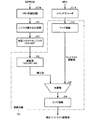
また本実施形態では図3(B)のD1に示すように、電源投入時(システムリセット時)に、リセット信号RESがアクティブになる。これにより、制御レジスタ30に表示特性制御パラメータが書き込まれ、制御レジスタ30のイニシャライズ処理が行われる。
【0100】
そして、図3(B)のD2、D3、D4に示すように、電源投入後(システムリセット後)に、リフレッシュ信号REFが定期的にアクティブになる。これにより、制御レジスタ30に表示特性制御パラメータが書き込まれ、制御レジスタ30のリフレッシュ処理が定期的に行われるようになる。
【0101】
このように、リフレッシュ処理を定期的に行うことで、表示パネル100の表示特性を安定して維持することが可能になる。
【0102】
なお、表示パネル100の表示動作に悪影響を与えない場合には、例えば非表示期間以外の期間においてリフレッシュ処理を定期的に行うようにしてもよい。
【0103】
5.制御レジスタ
図4に制御レジスタ30のレジスタマップの例を示す。
【0104】
図4において、E1に示す第1のレジスタ群(VOLDEF、DISCTL、GCPSET、REFPD、RDID)は、イニシャライズ処理或いはリフレッシュ処理の対象となるレジスタである。一方、E2に示す第2のレジスタ群(NOP、SWRESET、SLPIN、SLPOUT、PTLON、PTLAR、DISOFF、DISON、RAMWR、RAMRD)は、イニシャライズ処理或いはリフレッシュ処理の対象にならないレジスタである。これらの第1、第2のレジスタ群は、共に、MPU130によるアクセス(ライト動作)が可能になっている。
【0105】
そして、レジスタVOLDEF、DISCTL、GCPSETは、表示特性制御パラメータを記憶するレジスタである。具体的には、レジスタVOLDEFはコントラスト調整パラメータ(補正パラメータ)を記憶し、レジスタDISCTLは表示制御パラメータを記憶し、レジスタGCPSETは階調制御パラメータを記憶する。
【0106】
また、レジスタREFPDはリフレッシュ期間情報を記憶し、レジスタRDIDは製造情報を記憶する。
【0107】
一方、第2のレジスタ群の1つであるレジスタNOPは、MPU130が、走査線ドライバ(表示ドライバ)の非動作を指示するためのレジスタである(非動作指示コマンドのパラメータを記憶するレジスタ)。また、レジスタSWRESETは、ソフトウェアリセットを指示するためのレジスタであり、レジスタSLPIN、SLPOUTは、スリープイン動作、スリープアウト動作を指示するためのレジスタである。また、レジスタPTLON、PTLARはパーシャル表示、パーシャルエリアを指示するためのレジスタであり、レジスタDISOFF、DISONは、表示オフ、表示オンを指示するためのレジスタである。また、RAMWR、RAMRDは、図2の表示データRAM560のライト動作、リード動作を指示するためのレジスタである。
【0108】
ここで、レジスタVOLDEFが記憶するコントラスト調整パラメータは、後述するコントラスト調整の補正パラメータである。
【0109】
また、レジスタDISCTLが記憶する表示制御パラメータとしては、種々のものを考えることができる。
【0110】
例えば図5に示すように、表示制御パラメータ(DISCTL)には、表示ライン領域DRGの走査ライン数DLN、オフライン領域FRG1、FRG2の走査ライン数FLN1、FLN2、或いはデューティカウント(総ライン数)DUTYなどを含めることができる。
【0111】
また、表示制御パラメータ(DISCTL)には、表示パネル100の駆動方式を決めるパラメータを含めることができる。
【0112】
例えば図6(A)に示す1H(1水平走査期間)駆動方式と、図6(B)に示す0.5H駆動方式のいずれで駆動するかを、表示制御パラメータにより指定する。
【0113】
例えば、図6(A)、(B)において、ラッチパルス信号LPの立ち下がりエッジ間で1Hが規定される。そして、図6(A)では、1Hに1つのリセット信号GRESが生成される。一方、図6(B)では、1Hに2つのリセット信号GRESが生成され、1Hが0.5Hずつに分割される。そして、各0.5Hには、データ線ドライバでサポートできる最大階調数に応じた数(周波数)の階調制御パルスGCPが生成される。
【0114】
なお、図6(A)、(B)において、データ線出力であるパルス幅変調信号の立ち上がりは、リセット信号GRESの立ち下がりエッジにより規定される。一方、パルス幅変調信号の立ち下がりは、階調制御パルスGCPのパルスのうち、階調データに対応した位置のパルスにより規定されることになる。
【0115】
なお、表示制御パラメータにより指定できる駆動方式としては、種々のものを考えることができる。例えば、表示制御パラメータにより、PWM駆動とFRC(フレームレートコントロール)駆動の切替を行ってもよい。或いは、表示制御パラメータにより、極性反転方式(フレーム反転、ライン反転又はドット反転等)の切替を行ってもよい。
【0116】
図4の階調制御パラメータ(GCPSET)としては、種々のものを考えることができる。
【0117】
例えば図7に示すように、階調制御パルスがアクティブになる位置GCP1、GCP2・・・GCP63を設定するためのパラメータを、階調制御パラメータに含めることができる。これらの位置GCP1、GCP2・・・・GCP63を変更することで、表示パネル100の階調特性を、様々な特性に変更できる。
【0118】
なお、本実施形態における階調制御の駆動方式はPWM駆動に限定されず、FRC駆動などであってもよい。そして、例えば、階調制御パラメータに、FRC駆動を制御するための種々のパラメータ(フレームレート等)を含ませてもよい。
【0119】
図8(A)にリフレッシュ期間情報の例を示す。
【0120】
このリフレッシュ期間情報によれば、リフレッシュ処理を行わないという設定が可能となる。また、リフレッシュ期間として、例えば、64、128、192、256フレームなどを設定できる。例えば、64フレームを設定した場合には、64フレーム(Kフレーム)毎に定期的にリフレッシュ処理が行われるようになる。
【0121】
図8(A)に示すようなリフレッシュ期間情報を制御レジスタ30に書き込むことで、各表示パネルに応じた最適なリフレッシュ期間でリフレッシュ処理を行うことが可能になる。
【0122】
図8(B)に製造情報の例を示す。
【0123】
製造IDは、表示ドライバ(データ線ドライバ等)や表示パネルの製造ロットや製造工場などを特定するための情報である。製品バージョンは、表示ドライバや表示パネルの機種を特定するための情報である。製品番号は、個々の表示ドライバや個々の表示パネルを特定するための情報である。
【0124】
図8(B)に示すような製造情報を制御レジスタ30(RDID)に書き込むことで、表示ドライバや表示パネルに不具合が生じた場合に、その製造ロット、製造工場、製造バージョン、製品番号等を速やかに特定できるようになる。これにより、不具合の解析作業の効率化を図れる。
【0125】
即ち、制御レジスタ30はMPU130によりアクセス可能になっている。従って、不具合の解析作業時に、MPU130で動作するファームウェア(プログラム)を用いて、制御レジスタ30にアクセスし、製造情報を容易に得ることができる。従って、ICのパッケージを剥離して製造情報を確認する手法に比べて、不具合の解析作業を大幅に効率化できる。
【0126】
また本実施形態では、図8(B)の製造情報は、イニシャライズ処理時やリフレッシュ処理時にEEPROM134から制御レジスタ30(RDID)に自動的に書き込まれるようになっている。従って、製造情報の管理等も容易になる。
【0127】
6.レジスタ書き込み回路
図9に、レジスタ書き込み回路20の詳細な構成例を示す。このレジスタ書き込み回路20は、選択信号生成回路22、クロック供給回路24、26、セレクタSLC11、SLC12、SLC13、SLD11、SLD12、SLD13を含む。なお、図9の回路ブロックの一部を省略してもよい。
【0128】
図9において、制御レジスタ30が含むレジスタREG11、REG12、REG13・・・・は、図4のE1に示す第1のレジスタ群である。一方、REG21、REG22、REG23・・・・は、図4のE2に示す第2のレジスタ群である。また、端子Dはデータ端子であり、端子Cはクロック端子である。
【0129】
選択信号生成回路22は、リセット信号RES、リフレッシュ信号REFに基づいて選択信号SELを生成する。
【0130】
ここで、リセット信号RES、リフレッシュ信号REFは、図3(B)に示すように、リセットタイミング、リフレッシュタイミングでアクティブになる信号である。そして、選択信号生成回路22は、リセット信号RES、リフレッシュ信号REFのいずれかがアクティブになると、選択信号SELをアクティブにする。
【0131】
クロック供給回路24は、EEPROM134からの情報(表示特性制御パラメータ、リフレッシュ期間情報、製造情報等)を、レジスタREG11、REG12、REG13・・・・に書き込むためのクロック信号CA11、CA12、CA13・・・・を生成する。
【0132】
一方、クロック供給回路26は、MPU130からの情報(表示特性制御パラメータ、コマンドパラメータ等)を、レジスタREG11、REG12、REG13・・・・、REG21、REG22、REG23・・・・に書き込むためのクロック信号CB11、CB12、CB13・・・・、CB21、CB22、CB23・・・・を生成する。
【0133】
セレクタSLC11、SLC12、SLC13・・・・は、その選択端子Sに、選択信号生成回路22からの選択信号SELが入力される。また、その第1の入力端子Aに、クロック供給回路24からのクロック信号CA11、CA12、CA13・・・・が入力される。また、その第2の入力端子Bに、クロック供給回路26からのクロック信号CB11、CB12、CB13・・・・が入力される。
【0134】
そして、セレクタSLC11、SLC12、SLC13・・・・は、選択信号SELがアクティブになると、第1の入力端子A側を選択する。そして、クロック信号CA11、CA12、CA13・・・・を、クロック信号C11、C12、C13・・・・として、レジスタREG11、REG12、REG13・・・・のクロック端子Cに出力する。
【0135】
一方、セレクタSLC11、SLC12、SLC13・・・・は、選択信号SELが非アクティブになると、第2の入力端子B側を選択する。そして、クロック信号CB11、CB12、CB13・・・・を、クロック信号C11、C12、C13・・・・として、レジスタREG11、REG12、REG13・・・・のクロック端子Cに出力する。
【0136】
なお、レジスタREG21、REG22、REG23・・・・には、クロック供給回路26からのクロック信号CB21、CB22、CB23・・・・だけが入力されることになる。
【0137】
セレクタSLD11、SLD12、SLD13・・・・は、その選択端子Sに、選択信号生成回路22からの選択信号SELが入力される。また、その第1の入力端子Aに、メモリ制御回路579からのデータ(シリアルデータ)DMが入力される。また、その第2の入力端子Bに、コマンドデコーダ514からのデータ(シリアルデータ)が入力される。
【0138】
そして、セレクタSLD11、SLD12、SLD13・・・・は、選択信号SELがアクティブになると、第1の入力端子A側を選択する。そして、データDMを、データD11、D12、D13・・・・として、レジスタREG11、REG12、REG13・・・・のデータ端子Dに出力する。
【0139】
一方、セレクタSLD11、SLD12、SLD13・・・・は、選択信号SELが非アクティブになると、第2の入力端子B側を選択する。そして、データDCを、データD11、D12、D13・・・・として、レジスタREG11、REG12、REG13・・・・のデータ端子Dに出力する。
【0140】
図9の構成によれば、通常時においては、選択信号SELが非アクティブとなり、MPU130は、レジスタREG11、REG12、REG13・・・・、REG21、REG22、REG23・・・・にランダムアクセスできるようになる。そして、任意のレジスタに対して所望の情報を書き込むことができる。なお、この場合に、クロック供給回路26は、クロック信号CB11、CB12、CB13・・・・、CB21、CB22、CB23・・・・のうち、MPU130(コマンドデコーダ514)がアクセスしようとしているレジスタに対応するクロック信号だけを出力し、その他のクロック信号は非アクティブ(例えば常にローレベル)に設定する。
【0141】
一方、電源投入時(システムリセット時)又はリフレッシュ時には、選択信号SELがアクティブになる。この場合には、EEPROM134(メモリ制御回路579)からの情報が、第1のレジスタ群であるレジスタREG11、REG12、REG13・・・・にシーケンシャルに書き込まれるようになる。
【0142】
このようにすることで、電源投入時やリフレッシュ時に、表示特性制御パラメータ等をレジスタREG11、REG12、REG13・・・・に自動的に書き込むことが可能になる。
【0143】
なお、選択信号SELがアクティブになると、レジスタREG11、REG12、REG13・・・・に対するMPU130(処理部)のアクセスが禁止される。このアクセス禁止は、セレクタSLC11、SLC12、SLC13・・・・、SLD11、SLD12、SLD13・・・・が、第1の入力端子Aを選択することで実現される。
【0144】
このように、MPU130のアクセスを禁止することで、MPU130からのアクセスとEEPROM134からのアクセスが衝突して、レジスタREG11、REG12、REG13・・・・の内容が不確定になったり、不明になったりする事態を防止できる。
【0145】
7.コントラスト調整
図10に、図2の演算回路50の詳細な構成例を示す。この演算回路50は、減算器52、ラッチ回路54、加算器56、ラッチ回路58を含む。なお、図10の回路ブロックの一部を省略してもよい。
【0146】
EEPROM134から読み出された補正パラメータは、メモリ制御回路579、レジスタ書き込み回路20を介して、補正パラメータレジスタ40に書き込まれる。この補正パラメータレジスタ40は、図4のレジスタVOLDEFに相当し、コントラスト調整パラメータである補正パラメータを記憶する。
【0147】
そして、減算器52は、レジスタ40に書き込まれ補正パラメータの値(VOLDEF)から、コントラスト基準値である64を減算し、減算結果である補正値を出力する。
【0148】
一方、MPU130からコマンドデコーダ514を介して設定されたコントラスト調整値はラッチ回路54にラッチされる。そして、加算器56は、減算器52からの補正値とラッチ回路54からのコントラスト調整値を加算する。そして、加算結果である補正コントラスト調整値はラッチ回路58にラッチされる。
【0149】
このラッチされた補正コントラスト調整値は、例えば図2の電源制御回路578を介して、図1の電源回路132に出力される。そして、電源回路132は、補正コントラスト調整値に基づいて、電源電圧(例えば上側或いは下側の最大電源電圧)を生成し、データ線ドライバ110等に出力する。
【0150】
例えば図11に示すようにコントラスト範囲(0〜128)が設定されていたとする。この場合に、コントラスト基準値(64)は、コントラスト範囲の例えば中心値に設定されている。
【0151】
そして、液晶装置(電子機器)の検査時・出荷時に、図11に示す測定コントラスト基準値(例えば74)が測定される。すると、この測定コントラスト基準値(測定コントラストセンター値)は、補正パラメータとしてEEPROM134に書き込まれる。
【0152】
そして、この測定コントラスト基準値(74)は、EEPROM134、レジスタ書き込み回路20を介して、補正パラメータとしてレジスタ40に書き込まれる。すると、減算器52は、補正パラメータである測定コントラスト基準値(74)からコントラスト基準値(64)を減算し、補正値(10)を求める。
【0153】
一方、MPU130からのコントラスト調整値(例えば100)は、コマンドデコーダ514を介してラッチ回路54にラッチされる。すると、加算器56は、このコントラスト調整値(100)と、補正値(10)を加算して、補正コントラスト調整値(110)を求める。
【0154】
図12は、測定コントラスト基準値(50)が、コントラスト基準値(64)よりも下側にずれた場合の例である。この場合には、減算器52は、測定コントラスト基準値(50)からコントラスト基準値(64)を減算して、補正値(−14)を求める。そして、加算器56は、コントラスト調整値(100)に補正値(−14)を加算して、補正コントラスト調整値(86)を求める。
【0155】
以上のような本実施形態の手法によれば、MPU130上で動作するファームウェアは、測定コントラスト基準値のバラツキを、全く意識しなくて済むようになる。即ち、図11のように測定コントラスト基準値(表示特性)が上側にずれた場合にも、或いは図12のように下側にずれた場合にも、ファームウェアが設定したコントラスト基準値(100)に応じたコントラストで、表示パネル100を表示動作させることができる。
【0156】
また本実施形態では、電源投入時やシステムリセット時に、EEPROM134から読み出された測定コントラスト基準値(補正パラメータ)が、補正パラメータレジスタ40に自動的に書き込まれる。従って、MPU130上で動作するファームウェアは、電源投入時やシステムリセット時に、測定コントラスト基準値を補正パラメータレジスタ40に書き込む必要が無くなる。これにより、測定コントラスト基準値をファームウェアに記述しなくても済むようになる。また、表示パネルの機種が異なっても、同じファームウェアを使用できるようになる。
【0157】
また本実施形態では、所与のリフレッシュタイミングで、EEPROM134から読み出された測定コントラスト基準値が、補正パラメータレジスタ40に自動的に書き込まれる。これにより、静電気などの外部要因が発生した場合にも、表示パネル100のコントラスト特性を常に最適に維持できるようになる。
【0158】
なお、図10では、補正パラメータとして、測定コントラスト基準値をレジスタ40に書き込んでいるが、例えば、測定コントラスト基準値からコントラスト基準値(64)を減算することで得られる補正値を、レジスタ40に書き込んでもよい。この場合には、減算器52は不要になる
また、図11、図12では、コントラスト基準値をコントラスト範囲の略中心位置に設定しているが、それ以外の位置にコントラスト基準値を設定してもよい。
【0159】
図13に、液晶装置の出荷時や検査時に行われるパラメータ設定処理についてのフローチャートを示す。
【0160】
まず、コントラス(広義には表示特性)の調整を行い、コントラストを測定する(ステップS1、S2)。より具体的には、種々のコントラスト調整値を表示ドライバに設定し、表示パネルの明るさ等を測定する。
【0161】
次に、測定結果に基づいて、適正なコントラストを得られたか否かを判断する(ステップS3)。そして、得られなかった場合には、ステップS1に戻り、コントラスト調整を再度行う。
【0162】
一方、適正なコントラストが得られた場合には、その時の測定結果に基づいて、測定コントラスト基準値(広義には表示特性制御パラメータ)を求め、その測定コントラスト基準値をEEPROM134に書き込む。そして、液晶装置の検査を終了する。
【0163】
なお、本発明は本実施形態に限定されず、本発明の要旨の範囲内で種々の変形実施が可能である。
【0164】
例えば、明細書中の記載において広義な用語(メモリ、処理部、電気光学装置、表示ドライバ、表示特性、表示特性制御パラメータ等)として引用された用語(EEPROM、MPU、液晶装置、データ線ドライバ、コントラスト、測定コントラスト基準値等)は、明細書中の他の記載においても広義な用語に置き換えることができる。
【0165】
また、電気光学装置、表示ドライバ(データ線ドライバ)、レジスタ書き込み回路、制御レジスタ、演算回路の構成は、本実施形態で一例として説明されたものに限定されず、種々の変形実施が可能である。
【0166】
また、表示特性制御パラメータ、コントラスト調整パラメータ、表示制御パラメータ、階調制御パラメータ、リフレッシュ期間情報、製造情報、制御レジスタの内容、補正パラメータ等も、本実施形態で一例として説明されたものに限定されず、種々の変形実施が可能である。
【0167】
また、本実施形態では、電気光学材料として液晶を用いる液晶装置に本発明を適用した場合について説明した。しかしながら、本発明は、エレクトロルミネッセンス、蛍光表示管、プラズマディスプレイ、或いは有機ELなど電気光学効果を利用した電気光学装置にも広く適用できる。
【0168】
また、本実施形態における表示ドライバでは表示データRAMを内蔵するものとして説明したが、これに限定されるものではない。
【図面の簡単な説明】
【図1】電気光学装置の構成例を示すブロック図である。
【図2】データ線ドライバ(表示ドライバ)の構成例を示すブロック図である。
【図3】図3(A)、(B)は、リフレッシュタイミングについて説明するための図である。
【図4】制御レジスタについて説明するための図である。
【図5】表示制御パラメータについて説明するための図である。
【図6】図6(A)、(B)も、表示制御パラメータについて説明するための図である。
【図7】階調制御パラメータについて説明するための図である。
【図8】図8(A)、(B)は、リフレッシュ期間情報、製造情報について説明するための図である。
【図9】レジスタ書き込み回路の詳細例を示すブロック図である。
【図10】演算回路の詳細例を示すブロック図である。
【図11】コントラスト調整値の補正手法について説明するための図である。
【図12】コントラスト調整値の補正手法について説明するための図である。
【図13】パラメータ設定処理について説明するためのフローチャートである。
【符号の説明】
20 レジスタ書き込み回路
22 選択信号生成回路
24 クロック供給回路
26 クロック供給回路
SLC11〜SLC13 セレクタ
SLD11〜SLD13 セレクタ
REG11〜REG13 レジスタ
REG21〜REG23 レジスタ
30 制御レジスタ
40 補正パラメータレジスタ
50 演算回路
52 減算器
54 ラッチ回路
56 加算器
58 ラッチ回路
100 表示パネル
110 データ線ドライバ
120、122 走査線ドライバ
130 MPU(処理部)
132 電源回路
134 EEPROM(メモリ)
500 MPUインターフェース
502 入出力バッファ
512 バスホルダ
514 コマンドデコーダ
516 ステータスレジスタ
540 カラムアドレス制御回路
542 I/Oバッファ
550 ページアドレス制御回路
560 表示データRAM
570 ドライバ側制御回路
576 発振回路
580 PWMデコーダ回路
600 駆動回路[0001]
BACKGROUND OF THE INVENTION
The present invention relates to a display driver, an electro-optical device, and a parameter setting method for the display driver.
[0002]
[Background Art and Problems to be Solved by the Invention]
In a liquid crystal device (electro-optical device in a broad sense) used for electronic equipment such as a mobile phone, it is desired to perform a display operation with optimum display characteristics.
[0003]
However, since the display panel of the liquid crystal device has a variation in display characteristics, how to suppress the influence of this variation is an important technical problem.
[0004]
In addition, it is desired that the display characteristics of the liquid crystal device be optimally maintained even when external factors such as static electricity (ESD) occur.
[0005]
In an electronic device in which a liquid crystal device is incorporated, the firmware of the electronic device controls the display operation of the liquid crystal device. In this case, in order to shorten the development period of the electronic device, it is desired that the firmware creation work can be simplified as much as possible.
[0006]
SUMMARY An advantage of some aspects of the invention is that it provides a display driver, an electro-optical device, and a display driver parameter setting method capable of realizing appropriate display characteristics. is there.
[0007]
[Means for Solving the Problems]
The present invention is a display driver for driving a display panel, a control register for controlling the display driver, and a memory provided outside or inside the display driver for storing at least display characteristic control parameters. A display driver comprising: a memory control circuit that performs access control; and a register write circuit that writes a display characteristic control parameter read from the memory to the control register at a given refresh timing and performs a refresh process of the control register Related to.
[0008]
According to the present invention, the display characteristic control parameter read from the memory is written to the control register at a given refresh timing, and the control register is refreshed. Accordingly, display control of the display panel can be performed using an appropriate display characteristic control parameter, and appropriate display characteristics can be stably maintained.
[0009]
In the present invention, the register writing circuit may write a display characteristic control parameter to the control register and perform a refresh process of the control register during a non-display period of the display panel.
[0010]
In this case, the non-display period is, for example, a period in which the writing process to the control register does not adversely affect the display operation of the display panel. However, the refresh process can be performed in a period other than the non-display period.
[0011]
In the present invention, the register write circuit may periodically write the display characteristic control parameter to the control register after the power is turned on or the system is reset, and the control register is refreshed.
[0012]
Note that it is more desirable to perform a refresh process in a non-display period that occurs periodically.
[0013]
In the present invention, the memory stores period information of a refresh process performed by the register write circuit, and the register write circuit writes the period information read from the memory to the control register. Also good.
[0014]
In the present invention, the register writing circuit may write the display characteristic control parameter read from the memory to the control register at power-on or system reset, and perform initialization processing of the control register. .
[0015]
The present invention also provides a display driver for driving a display panel, a control register for controlling the display driver, and a memory that is provided outside or inside the display driver and stores at least display characteristic control parameters. A memory control circuit that performs access control, and a register write circuit that writes a display characteristic control parameter read from the memory to the control register and initializes the control register at power-on or system reset Related to display driver.
[0016]
According to the present invention, when the power is turned on or the system is reset, the display characteristic control parameter read from the memory is written to the control register, and the control register is initialized. Therefore, according to the present invention, it is possible to automatically read an appropriate display characteristic control parameter and perform display control of the display panel.
[0017]
In the present invention, the control register may include a first register group that stores display characteristic control parameters and is accessible by the processing unit, and a second register group that is accessible by the processing unit.
[0018]
In this case, information other than the display control parameter (for example, various command information related to display) can be stored in the second register group.
[0019]
In the present invention, the register writing circuit may prohibit the processing unit from accessing the first register group when the display characteristic control parameter is being written to the first register group. .
[0020]
In this way, it is possible to prevent a situation where access from the processing unit and access from the memory collide.
[0021]
In the present invention, the memory may store manufacturing information of a display driver or a display panel, and the register writing circuit may write manufacturing information read from the memory to the control register.
[0022]
In this case, as the manufacturing information, for example, manufacturing identification information, product version information, or product specifying information can be included.
[0023]
In the present invention, the display characteristic control parameter may include at least one of a contrast adjustment parameter, a display control parameter, and a gradation control parameter.
[0024]
However, it is possible to include other parameters as display characteristic control parameters.
[0025]
In the present invention, the display characteristic control parameter may be a parameter having a different value for each display panel or for each display panel model.
[0026]
The electro-optical device of the present invention relates to an electro-optical device including any of the display drivers described above, a display panel driven by the display driver, and a processing unit that controls the operation of the display driver.
[0027]
The present invention is also the display driver parameter setting method according to any one of the above, wherein the display characteristic of the display panel driven by the display driver is measured, and the display characteristic control parameter specified by the measurement is stored in the memory. It relates to the parameter setting method to be written.
[0028]
DETAILED DESCRIPTION OF THE INVENTION
DESCRIPTION OF EXEMPLARY EMBODIMENTS Hereinafter, preferred embodiments of the invention will be described in detail with reference to the drawings. The embodiments described below do not unduly limit the contents of the present invention described in the claims. Also, not all of the configurations described below are essential constituent requirements of the present invention.
[0029]
1. Electro-optic device
FIG. 1 shows a configuration example of the electro-optical device according to the present embodiment.
[0030]
This electro-optical device (liquid crystal device in a narrow sense) includes a display panel 100 (a liquid crystal panel in a narrow sense).
[0031]
The
[0032]
Note that the
[0033]
The electro-optical device also includes a data line driver 110 (data line driving circuit, X driver, source driver) and
[0034]
Here, the
[0035]
Note that the
[0036]
The electro-optical device includes an MPU 130 (a processing unit in a broad sense).
[0037]
Here, the MPU (Micro Processor Unit) 130 controls the
[0038]
More specifically, the
[0039]
The MPU 130 (processing unit) may be realized by a general-purpose processor (CPU) or a controller circuit that is an ASIC.
[0040]
Further, the functions of the
[0041]
The
[0042]
The EEPROM 134 (memory, nonvolatile memory or ROM in a broad sense) stores various kinds of information for operating the electro-optical device.
[0043]
More specifically, the
[0044]
Note that the
[0045]
Further, some or all of the
[0046]
2. Data line driver
FIG. 2 shows a configuration example of the data line driver 110 (display driver or display drive circuit in a broad sense) of the present embodiment. Note that the
[0047]
The
[0048]
For example, 8-bit data (commands) D7 to D0 are input to the input /
[0049]
The
[0050]
The
[0051]
The
[0052]
The MPU
[0053]
The column
[0054]
The page
[0055]
Based on the oscillation output from the
[0056]
The
[0057]
The
[0058]
With this configuration, in the present embodiment, various images can be displayed on the
[0059]
3. Display characteristic control parameter initialization and refresh
Now, in a liquid crystal device (electro-optical device) used in an electronic device such as a mobile phone, it is desirable to adjust display characteristics (contrast, hue, etc.) of the display panel at the time of inspection and shipment. And after optimal adjustment is performed, it is desirable to ship to the manufacturer of an electronic device, and to incorporate in an electronic device.
[0060]
In this case, for the manufacturer of the electric equipment, it is only necessary that the display characteristics of the display panel are optimum, and there is no interest in the setting contents of the display characteristics. If the display characteristic setting is performed by the firmware, the display characteristic setting description part in the firmware must be changed for each display panel or each display panel model. For this reason, there is a possibility that the manufacturer of the electric device may be forced to perform unnecessary and complicated work.
[0061]
Moreover, in an electronic device such as a mobile phone, various external factors such as static electricity (ESD) are generated depending on the usage state. If the set display characteristics are changed due to this external factor, the optimum display characteristics may not be maintained.
[0062]
Therefore, in the present embodiment, the various problems described above are solved by adopting a configuration as described below.
[0063]
That is, the
[0064]
The
[0065]
More specifically, the
[0066]
In the
[0067]
Here, the
[0068]
More specifically, when the
[0069]
By providing such a
[0070]
The control register 30 may be realized by a holding circuit such as a D flip-flop, or may be realized by a memory such as a RAM.
[0071]
In the present embodiment, the
[0072]
More specifically, the
[0073]
By performing such initialization processing, the display characteristic control parameter stored in the
[0074]
Therefore, the MPU
[0075]
Further, the firmware (program) operating on the MPU 130 (processing unit) does not need to write display characteristic control parameters to the
[0076]
In this embodiment, the
[0077]
By doing so, the display characteristics of the
[0078]
That is, in an electronic device such as a mobile phone, the display characteristic control parameter of the
[0079]
In this embodiment, even in such a case, the optimum display characteristic control parameter stored in the
[0080]
In the present embodiment, in order to simplify the contrast adjustment process, the
[0081]
Here, the
[0082]
In this embodiment, the correction parameter stored in the
[0083]
The
[0084]
That is, in this embodiment, the contrast adjustment value is set by the
[0085]
Then, the
[0086]
4). Refresh timing
In the present embodiment, the
[0087]
More specifically, in the present embodiment, as shown in FIG. 3A, the
[0088]
Here, the display line region DRG is a region where an image is actually displayed. On the other hand, the offline areas FRG1 and FRG2 are areas (dummy areas) where no image is displayed.
[0089]
For example, it is assumed that the upper offline area FRG1 does not exist. In this case, in the uppermost first scanning line of the display line region DRG, the second scanning line exists below the first scanning line, but the scanning line does not exist above the first scanning line. On the other hand, in the second scanning line, there is a third scanning line on the lower side, and there is also a first scanning line on the upper side. Therefore, when the offline region FRG1 does not exist, the parasitic capacitance and the like are different between the first scanning line and the second scanning line, and the display state of the portion is uneven.
[0090]
On the other hand, if the off-line region FRG1 as shown in FIG. 3A is provided, a dummy scan line also exists on the first scan line. As a result, the parasitic capacitances of the first and second scan lines can be made substantially the same, and uneven display can be prevented.
[0091]
Similarly, if the lower offline region FRG2 is provided, the parasitic capacitance and the like are substantially the same in the lowermost Nth scanning line of the display line region DRG and the uppermost N-1th scanning line. It is possible to prevent unevenness in the display state.
[0092]
The offline areas FRG1 and FRG2 are provided for the following purposes, for example.
[0093]
That is, the number of display lines on the display panel 100 (the number of lines in the display line region DRG) is generally different for each model of electronic device.
[0094]
In this case, if the
[0095]
If the offline regions FRG1 and FRG2 as shown in FIG. 3A are provided, the number of scanning lines in the offline regions FRG1 and FRG2 is variably changed, and a part of the scanning lines of the FRG1 and FRG2 is changed in the display line region DRG. It becomes possible to assign to the scanning (display) line. As a result, even if the model of the electronic device changes and the number of display lines on the
[0096]
In the present embodiment, as indicated by C1 in FIG. 3A, the refresh process of the
[0097]
That is, if the refresh process of the
[0098]
In C1 of FIG. 3A, the refresh process is performed at the scan timing of the last scan line in the offline area FRG2, but the refresh process may be performed at the scan timing of the first scan line in the offline area FRG1. . Alternatively, the refresh process may be performed at a scan timing of a scan line (FRG1, FRG2) different from these scan lines.
[0099]
In this embodiment, as indicated by D1 in FIG. 3B, the reset signal RES becomes active when the power is turned on (system reset). As a result, the display characteristic control parameter is written into the
[0100]
Then, as indicated by D2, D3, and D4 in FIG. 3B, the refresh signal REF periodically becomes active after power-on (after system reset). As a result, the display characteristic control parameter is written into the
[0101]
Thus, by periodically performing the refresh process, the display characteristics of the
[0102]
In the case where the display operation of the
[0103]
5. Control register
FIG. 4 shows an example of a register map of the
[0104]
In FIG. 4, a first register group (VOLDEF, DISCTL, GCPSET, REFPD, RDID) indicated by E1 is a register to be subjected to initialization processing or refresh processing. On the other hand, the second register group (NOP, SWRESET, SLPIN, SLPOUT, PTLON, PTLAR, DISOFF, DISON, RAMWR, RAMRD) indicated by E2 is a register that is not an object of initialization processing or refresh processing. Both of these first and second register groups can be accessed (write operation) by the
[0105]
The registers VOLDEF, DISCTL, and GCPSET are registers that store display characteristic control parameters. Specifically, the register VOLDEF stores a contrast adjustment parameter (correction parameter), the register DISCTL stores a display control parameter, and the register GCPSET stores a gradation control parameter.
[0106]
The register REFPD stores refresh period information, and the register RDID stores manufacturing information.
[0107]
On the other hand, the register NOP, which is one of the second register groups, is a register for the
[0108]
Here, the contrast adjustment parameter stored in the register VOLDEF is a correction parameter for contrast adjustment described later.
[0109]
Various display control parameters stored in the register DISCTL can be considered.
[0110]
For example, as shown in FIG. 5, the display control parameter (DISCTL) includes the number of scanning lines DLN in the display line area DRG, the number of scanning lines FLN1, FLN2 in the offline areas FRG1, FRG2, or the duty count (total number of lines) DUTY. Can be included.
[0111]
Further, the display control parameter (DISCTL) can include a parameter that determines the driving method of the
[0112]
For example, one of the 1H (one horizontal scanning period) driving method shown in FIG. 6A and the 0.5H driving method shown in FIG. 6B is designated by the display control parameter.
[0113]
For example, in FIGS. 6A and 6B, 1H is defined between falling edges of the latch pulse signal LP. In FIG. 6A, one reset signal GRES is generated at 1H. On the other hand, in FIG. 6B, two reset signals GRES are generated in 1H, and 1H is divided into 0.5H. In each 0.5H, a number (frequency) of gradation control pulses GCP corresponding to the maximum number of gradations that can be supported by the data line driver is generated.
[0114]
6A and 6B, the rising edge of the pulse width modulation signal, which is the data line output, is defined by the falling edge of the reset signal GRES. On the other hand, the fall of the pulse width modulation signal is defined by the pulse at the position corresponding to the gradation data among the gradation control pulse GCP.
[0115]
Various driving methods that can be specified by the display control parameter can be considered. For example, switching between PWM driving and FRC (frame rate control) driving may be performed according to display control parameters. Alternatively, the polarity inversion method (frame inversion, line inversion, dot inversion, etc.) may be switched according to the display control parameter.
[0116]
Various gradation control parameters (GCPSET) in FIG. 4 can be considered.
[0117]
For example, as shown in FIG. 7, parameters for setting positions GCP1, GCP2,... GCP63 at which the gradation control pulse becomes active can be included in the gradation control parameters. By changing these positions GCP1, GCP2,... GCP63, the gradation characteristics of the
[0118]
Note that the gradation control driving method in the present embodiment is not limited to PWM driving, and may be FRC driving or the like. For example, various parameters (such as a frame rate) for controlling the FRC drive may be included in the gradation control parameter.
[0119]
FIG. 8A shows an example of refresh period information.
[0120]
According to the refresh period information, it is possible to set not to perform the refresh process. Further, for example, 64, 128, 192, 256 frames, etc. can be set as the refresh period. For example, when 64 frames are set, the refresh process is periodically performed every 64 frames (K frames).
[0121]
By writing the refresh period information as shown in FIG. 8A into the
[0122]
FIG. 8B shows an example of manufacturing information.
[0123]
The manufacturing ID is information for specifying a display driver (data line driver or the like), a manufacturing lot of a display panel, a manufacturing factory, or the like. The product version is information for specifying the model of the display driver and the display panel. The product number is information for specifying individual display drivers and individual display panels.
[0124]
When manufacturing information such as shown in FIG. 8B is written in the control register 30 (RDID), when a malfunction occurs in the display driver or display panel, the manufacturing lot, manufacturing factory, manufacturing version, product number, etc. It becomes possible to identify quickly. As a result, the efficiency of the failure analysis work can be improved.
[0125]
That is, the
[0126]
In the present embodiment, the manufacturing information in FIG. 8B is automatically written from the
[0127]
6). Register write circuit
FIG. 9 shows a detailed configuration example of the
[0128]
9, registers REG11, REG12, REG13,... Included in the
[0129]
The selection
[0130]
Here, as shown in FIG. 3B, the reset signal RES and the refresh signal REF are signals that become active at the reset timing and the refresh timing. The selection
[0131]
The
[0132]
On the other hand, the
[0133]
The selectors SLC11, SLC12, SLC13,... Receive the selection signal SEL from the selection
[0134]
The selectors SLC11, SLC12, SLC13,... Select the first input terminal A side when the selection signal SEL becomes active. The clock signals CA11, CA12, CA13,... Are output to the clock terminals C of the registers REG11, REG12, REG13,.
[0135]
On the other hand, the selectors SLC11, SLC12, SLC13,... Select the second input terminal B side when the selection signal SEL becomes inactive. The clock signals CB11, CB12, CB13,... Are output to the clock terminals C of the registers REG11, REG12, REG13,.
[0136]
.., Only the clock signals CB21, CB22, CB23... From the
[0137]
The selectors SLD11, SLD12, SLD13,... Receive the selection signal SEL from the selection
[0138]
Then, the selectors SLD11, SLD12, SLD13,... Select the first input terminal A side when the selection signal SEL becomes active. The data DM is output to the data terminal D of the registers REG11, REG12, REG13,... As data D11, D12, D13,.
[0139]
On the other hand, the selectors SLD11, SLD12, SLD13,... Select the second input terminal B side when the selection signal SEL becomes inactive. Then, the data DC is output as data D11, D12, D13... To the data terminal D of the registers REG11, REG12, REG13.
[0140]
9, the selection signal SEL is inactive during normal times so that the
[0141]
On the other hand, the selection signal SEL becomes active when the power is turned on (system reset) or at the time of refresh. In this case, information from the EEPROM 134 (memory control circuit 579) is sequentially written into the registers REG11, REG12, REG13,.
[0142]
This makes it possible to automatically write display characteristic control parameters and the like to the registers REG11, REG12, REG13,.
[0143]
When the selection signal SEL becomes active, access of the MPU 130 (processing unit) to the registers REG11, REG12, REG13,. This access prohibition is realized by the selectors SLC11, SLC12, SLC13,..., SLD11, SLD12, SLD13,.
[0144]
As described above, by prohibiting the access of the
[0145]
7). Contrast adjustment
FIG. 10 shows a detailed configuration example of the
[0146]
The correction parameter read from the
[0147]
The
[0148]
On the other hand, the contrast adjustment value set from the
[0149]
The latched corrected contrast adjustment value is output to the
[0150]
For example, it is assumed that the contrast range (0 to 128) is set as shown in FIG. In this case, the contrast reference value (64) is set to, for example, the center value of the contrast range.
[0151]
Then, at the time of inspection and shipment of the liquid crystal device (electronic device), a measured contrast reference value (for example, 74) shown in FIG. 11 is measured. Then, this measured contrast reference value (measured contrast center value) is written in the
[0152]
The measured contrast reference value (74) is written into the
[0153]
On the other hand, the contrast adjustment value (for example, 100) from the
[0154]
FIG. 12 shows an example in which the measured contrast reference value (50) is shifted downward from the contrast reference value (64). In this case, the
[0155]
According to the method of this embodiment as described above, the firmware operating on the
[0156]
In this embodiment, the measured contrast reference value (correction parameter) read from the
[0157]
In the present embodiment, the measured contrast reference value read from the
[0158]
In FIG. 10, the measurement contrast reference value is written in the
In FIGS. 11 and 12, the contrast reference value is set at the approximate center position of the contrast range, but the contrast reference value may be set at other positions.
[0159]
FIG. 13 shows a flowchart of parameter setting processing performed at the time of shipment or inspection of the liquid crystal device.
[0160]
First, contrast (display characteristics in a broad sense) is adjusted and the contrast is measured (steps S1 and S2). More specifically, various contrast adjustment values are set in the display driver, and the brightness of the display panel is measured.
[0161]
Next, based on the measurement result, it is determined whether or not an appropriate contrast has been obtained (step S3). If not obtained, the process returns to step S1 and contrast adjustment is performed again.
[0162]
On the other hand, when an appropriate contrast is obtained, a measurement contrast reference value (display characteristic control parameter in a broad sense) is obtained based on the measurement result at that time, and the measurement contrast reference value is written in the
[0163]
In addition, this invention is not limited to this embodiment, A various deformation | transformation implementation is possible within the range of the summary of this invention.
[0164]
For example, terms (EEPROM, MPU, liquid crystal device, data line driver) cited as broad terms (memory, processing unit, electro-optical device, display driver, display characteristic, display characteristic control parameter, etc.) in the description in the specification Contrast, measured contrast reference value, etc.) can be replaced by broad terms in other descriptions in the specification.
[0165]
The configurations of the electro-optical device, the display driver (data line driver), the register writing circuit, the control register, and the arithmetic circuit are not limited to those described as an example in the present embodiment, and various modifications can be made. .
[0166]
In addition, display characteristic control parameters, contrast adjustment parameters, display control parameters, gradation control parameters, refresh period information, manufacturing information, control register contents, correction parameters, and the like are also limited to those described as examples in this embodiment. However, various modifications can be made.
[0167]
In the present embodiment, the case where the present invention is applied to a liquid crystal device using liquid crystal as an electro-optical material has been described. However, the present invention can be widely applied to an electro-optical device using an electro-optical effect such as electroluminescence, a fluorescent display tube, a plasma display, or an organic EL.
[0168]
Further, although the display driver in the present embodiment has been described as including the display data RAM, the present invention is not limited to this.
[Brief description of the drawings]
FIG. 1 is a block diagram illustrating a configuration example of an electro-optical device.
FIG. 2 is a block diagram illustrating a configuration example of a data line driver (display driver).
3A and 3B are diagrams for explaining refresh timing. FIG.
FIG. 4 is a diagram for explaining a control register;
FIG. 5 is a diagram for explaining display control parameters;
6A and 6B are also diagrams for explaining display control parameters. FIG.
FIG. 7 is a diagram for explaining gradation control parameters.
8A and 8B are diagrams for explaining refresh period information and manufacturing information. FIG.
FIG. 9 is a block diagram illustrating a detailed example of a register write circuit.
FIG. 10 is a block diagram illustrating a detailed example of an arithmetic circuit.
FIG. 11 is a diagram for explaining a method for correcting a contrast adjustment value.
FIG. 12 is a diagram for explaining a method for correcting a contrast adjustment value.
FIG. 13 is a flowchart for explaining parameter setting processing;
[Explanation of symbols]
20 register write circuit
22 Selection signal generation circuit
24 Clock supply circuit
26 Clock supply circuit
SLC11-SLC13 selector
SLD11-SLD13 selector
REG11 to REG13 registers
REG21 to REG23 registers
30 Control register
40 Correction parameter register
50 arithmetic circuit
52 Subtractor
54 Latch circuit
56 Adder
58 Latch circuit
100 Display panel
110 Data line driver
120, 122 Scan line driver
130 MPU (Processor)
132 Power supply circuit
134 EEPROM (memory)
500 MPU interface
502 I / O buffer
512 bus holder
514 Command decoder
516 Status register
540 column address control circuit
542 I / O buffer
550 Page address control circuit
560 display data RAM
570 Driver side control circuit
576 oscillator circuit
580 PWM decoder circuit
600 Drive circuit
Claims (14)
表示ドライバを制御するための制御レジスタと、
表示ドライバの外部又は内部に設けられ表示特性制御パラメータを少なくとも記憶するメモリに対して、アクセス制御を行うメモリ制御回路と、
所与のリフレッシュタイミングで、前記メモリから読み出された表示特性制御パラメータを前記制御レジスタに書き込み、前記制御レジスタのリフレッシュ処理を行うレジスタ書き込み回路とを含み、
前記制御レジスタが、
処理部によりアクセス可能であり、前記リフレッシュ処理の対象となる第1のレジスタ群と、前記処理部によりアクセス可能であり、前記リフレッシュ処理の対象とならない第2のレジスタ群を含み、
前記レジスタ書き込み回路が、
その選択端子に、前記リフレッシュタイミングでアクティブになる選択信号が入力され、その第1の入力端子に、前記メモリ制御回路からの情報が入力され、その第2の入力端子に、前記処理部からの情報が入力されるセレクタを含み、
前記選択信号がアクティブになるリフレッシュ時には、前記メモリ制御回路からの情報である前記表示特性制御パラメータが前記セレクタを介して前記第1のレジスタ群に書き込まれ、
前記選択信号が非アクティブになる通常時には、前記処理部からの情報が前記セレクタを介して前記第1のレジスタ群に書き込まれることを特徴とする表示ドライバ。A display driver for driving a display panel,
A control register for controlling the display driver;
A memory control circuit that controls access to a memory that is provided outside or inside the display driver and stores at least display characteristic control parameters;
A register writing circuit that writes display characteristic control parameters read from the memory to the control register at a given refresh timing, and performs refresh processing of the control register ;
The control register is
A first register group that is accessible by a processing unit and is a target of the refresh process; and a second register group that is accessible by the processing unit and is not a target of the refresh process;
The register write circuit
A selection signal that becomes active at the refresh timing is input to the selection terminal, information from the memory control circuit is input to the first input terminal, and information from the processing unit is input to the second input terminal. Including a selector into which information is entered,
At the time of refresh when the selection signal becomes active, the display characteristic control parameter which is information from the memory control circuit is written to the first register group via the selector,
A display driver characterized in that information from the processing unit is written to the first register group via the selector at a normal time when the selection signal becomes inactive .
前記メモリが、 The memory is
リフレッシュ処理を行わないという設定と、リフレッシュ処理を行う場合にそのリフレッシュ期間の設定とを行うためのリフレッシュ期間情報を記憶し、 Stores refresh period information for setting the refresh process not to be performed and setting the refresh period when the refresh process is performed,
前記レジスタ書き込み回路が、 The register write circuit
前記メモリから読み出された前記リフレッシュ期間情報を、前記制御レジスタの前記第1のレジスタ群に書き込み、前記リフレッシュ期間情報によりリフレッシュ処理を行うことが設定されていた場合にリフレッシュ処理を行うことを特徴とする表示ドライバ。 The refresh period information read from the memory is written into the first register group of the control register, and the refresh process is performed when the refresh process is set to be performed according to the refresh period information. Display driver.
前記表示パネルには、表示ライン領域と、前記表示ライン領域の上側に設けられその走査ライン数が可変な第1のオフライン領域と、前記表示ライン領域の下側に設けられその走査ライン数が可変な第2のオフライン領域とが設定され、 The display panel includes a display line area, a first offline area provided above the display line area and having a variable number of scanning lines, and provided below the display line area and having a variable number of scanning lines. Second offline area is set,
前記レジスタ書き込み回路が、 The register write circuit
前記第1のオフライン領域の最初の走査ラインのスキャンタイミング又は前記第2のオフライン領域の最後の走査ラインのスキャンタイミングでリフレッシュ処理を行うことを特徴とする表示ドライバ。 A display driver, wherein refresh processing is performed at a scan timing of the first scan line in the first offline area or a scan timing of the last scan line in the second offline area.
前記メモリが、The memory is
前記表示ライン領域の走査ライン数である第1の走査ライン数と、前記第1、第2のオフライン領域の走査ライン数である第2、第3の走査ライン数を記憶し、 Storing the number of first scanning lines which is the number of scanning lines in the display line area and the number of second and third scanning lines which are the number of scanning lines in the first and second offline areas;
前記レジスタ書き込み回路が、 The register write circuit
前記メモリから読み出された前記第1、第2、第3の走査ライン数を前記制御レジスタの前記第1のレジスタ群に書き込むことを特徴とする表示ドライバ。 A display driver, wherein the first, second, and third scan line numbers read from the memory are written to the first register group of the control register.
処理部用インターフェースを介して前記処理部から入力されたコマンドをデコードするコマンドデコーダを含み、 A command decoder for decoding a command input from the processing unit via the processing unit interface;
前記制御レジスタには、前記コマンドデコーダからのデコード結果情報が前記処理部からの情報として書き込まれることを特徴とする表示ドライバ。 Decoding result information from the command decoder is written in the control register as information from the processing unit.
前記レジスタ書き込み回路が、
表示パネルの非表示期間において、表示特性制御パラメータを前記制御レジスタに書き込み、前記制御レジスタのリフレッシュ処理を行うことを特徴とする表示ドライバ。In any one of Claims 1 thru | or 5 ,
The register write circuit
A display driver, wherein a display characteristic control parameter is written to the control register and a refresh process of the control register is performed during a non-display period of the display panel.
前記レジスタ書き込み回路が、
電源投入後又はシステムリセット後に、定期的に、表示特性制御パラメータを前記制御レジスタに書き込み、前記制御レジスタのリフレッシュ処理を行うことを特徴とする表示ドライバ。In any one of Claims 1 thru | or 6 .
The register write circuit
A display driver characterized by periodically writing display characteristic control parameters into the control register after power-on or system reset, and refreshing the control register.
前記レジスタ書き込み回路が、
電源投入時又はシステムリセット時に、前記メモリから読み出された表示特性制御パラメータを前記制御レジスタに書き込み、前記制御レジスタのイニシャライズ処理を行うことを特徴とする表示ドライバ。In any one of Claims 1 thru | or 7 ,
The register write circuit
A display driver, wherein a display characteristic control parameter read from the memory is written to the control register at power-on or system reset, and initialization processing of the control register is performed.
前記レジスタ書き込み回路が、
前記第1のレジスタ群に表示特性制御パラメータを書き込んでいる際には、該第1のレジスタ群への処理部のアクセスを禁止することを特徴とする表示ドライバ。In any one of Claims 1 thru | or 8 .
The register write circuit
A display driver characterized in that, when a display characteristic control parameter is written in the first register group, access of the processing unit to the first register group is prohibited.
前記メモリが、
表示ドライバ又は表示パネルの製造情報を記憶し、
前記レジスタ書き込み回路が、
前記メモリから読み出された製造情報を、前記制御レジスタに書き込むことを特徴とする表示ドライバ。In any one of Claims 1 thru | or 9 ,
The memory is
Stores display driver or display panel manufacturing information,
The register write circuit
A display driver, wherein manufacturing information read from the memory is written to the control register.
前記表示特性制御パラメータが、
コントラスト調整パラメータ、表示制御パラメータ、及び階調制御パラメータの少なくとも1つを含むことを特徴とする表示ドライバ。In any one of Claims 1 thru | or 10 .
The display characteristic control parameter is
A display driver comprising at least one of a contrast adjustment parameter, a display control parameter, and a gradation control parameter.
前記表示特性制御パラメータが、
表示パネル毎に又は表示パネルの機種毎にその値が異なるパラメータであることを特徴とする表示ドライバ。In any one of Claims 1 thru | or 11 ,
The display characteristic control parameter is
A display driver characterized in that the parameter is different for each display panel or each display panel model.
前記表示ドライバにより駆動される表示パネルと、
前記表示ドライバの動作を制御する処理部と、
を含むことを特徴とする電気光学装置。A display driver according to any one of claims 1 to 12 ,
A display panel driven by the display driver;
A processing unit for controlling the operation of the display driver;
An electro-optical device comprising:
表示ドライバにより駆動される表示パネルの表示特性を測定し、
測定により特定される表示特性制御パラメータを、前記メモリに書き込むことを特徴とする表示ドライバのパラメータ設定方法。A display driver parameter setting method according to any one of claims 1 to 12 ,
Measure the display characteristics of the display panel driven by the display driver,
A display driver parameter setting method, wherein a display characteristic control parameter specified by measurement is written in the memory.
Priority Applications (4)
| Application Number | Priority Date | Filing Date | Title |
|---|---|---|---|
| JP2002061468A JP3636148B2 (en) | 2002-03-07 | 2002-03-07 | Display driver, electro-optical device, and display driver parameter setting method |
| US10/376,333 US7151522B2 (en) | 2002-03-07 | 2003-03-03 | Display driver, electro-optical device, and method of setting display driver parameters |
| EP03004870A EP1343136A1 (en) | 2002-03-07 | 2003-03-06 | Display driver, electro-optical device, and method of setting display driver parameters |
| CNB031205070A CN100383836C (en) | 2002-03-07 | 2003-03-07 | Display drive, electrooptical device and parameter setting method of display drive |
Applications Claiming Priority (1)
| Application Number | Priority Date | Filing Date | Title |
|---|---|---|---|
| JP2002061468A JP3636148B2 (en) | 2002-03-07 | 2002-03-07 | Display driver, electro-optical device, and display driver parameter setting method |
Publications (2)
| Publication Number | Publication Date |
|---|---|
| JP2003263134A JP2003263134A (en) | 2003-09-19 |
| JP3636148B2 true JP3636148B2 (en) | 2005-04-06 |
Family
ID=27751194
Family Applications (1)
| Application Number | Title | Priority Date | Filing Date |
|---|---|---|---|
| JP2002061468A Expired - Lifetime JP3636148B2 (en) | 2002-03-07 | 2002-03-07 | Display driver, electro-optical device, and display driver parameter setting method |
Country Status (4)
| Country | Link |
|---|---|
| US (1) | US7151522B2 (en) |
| EP (1) | EP1343136A1 (en) |
| JP (1) | JP3636148B2 (en) |
| CN (1) | CN100383836C (en) |
Cited By (1)
| Publication number | Priority date | Publication date | Assignee | Title |
|---|---|---|---|---|
| KR101203693B1 (en) * | 2006-10-10 | 2012-11-21 | 삼성전자주식회사 | Method for automatic recovering control register bit values and LCD driver integrated circuit for the same |
Families Citing this family (25)
| Publication number | Priority date | Publication date | Assignee | Title |
|---|---|---|---|---|
| GB0215125D0 (en) * | 2002-06-28 | 2002-08-07 | Delphi Tech Inc | Control method for a liquid crystal display |
| JP4501377B2 (en) * | 2003-08-21 | 2010-07-14 | カシオ計算機株式会社 | Display device |
| JP4016915B2 (en) * | 2003-09-11 | 2007-12-05 | 株式会社日立製作所 | Display system and display panel and signal processing device used therefor |
| JP4062256B2 (en) * | 2004-01-05 | 2008-03-19 | セイコーエプソン株式会社 | Display driver and electronic device including display driver |
| JP4501480B2 (en) * | 2004-03-19 | 2010-07-14 | セイコーエプソン株式会社 | Electro-optical device, control device for electro-optical device, control method for electro-optical device, and electronic apparatus |
| US20060017669A1 (en) * | 2004-07-20 | 2006-01-26 | Eastman Kodak Company | Method and apparatus for uniformity and brightness correction in an OLED display |
| CN100399402C (en) * | 2004-09-14 | 2008-07-02 | 友达光电股份有限公司 | Time sequence controller with external transmission interface and electronic product using said controller |
| KR20060065943A (en) * | 2004-12-11 | 2006-06-15 | 삼성전자주식회사 | Method for driving of display device, and display control device and display device for performing the same |
| JP2006308900A (en) * | 2005-04-28 | 2006-11-09 | Seiko Epson Corp | Display controller, display system, and display control method |
| JP5518111B2 (en) * | 2005-05-06 | 2014-06-11 | キヤノン株式会社 | Digital camera |
| JP5006568B2 (en) * | 2005-05-06 | 2012-08-22 | キヤノン株式会社 | Register setting control device, register setting control method, program, and digital camera |
| JP5057417B2 (en) * | 2005-05-30 | 2012-10-24 | ルネサスエレクトロニクス株式会社 | Semiconductor integrated circuit for liquid crystal display drive |
| US20070024744A1 (en) * | 2005-07-26 | 2007-02-01 | Kaehler John W | System and method for periodic reset of a display |
| JP4830424B2 (en) * | 2005-09-27 | 2011-12-07 | カシオ計算機株式会社 | Drive device |
| JP5019194B2 (en) * | 2005-11-30 | 2012-09-05 | 株式会社ジャパンディスプレイセントラル | Display control circuit |
| US7447096B2 (en) * | 2006-05-05 | 2008-11-04 | Honeywell International Inc. | Method for refreshing a non-volatile memory |
| KR100824796B1 (en) | 2006-07-03 | 2008-04-24 | 삼성전자주식회사 | Data error correction circuits and methods thereof, and integrated circuits having the same |
| US20080043002A1 (en) * | 2006-08-15 | 2008-02-21 | Kaehler John W | Systems and methods for alternative to serial peripheral interface communication in dumb display driver integrated circuits |
| JP2009037074A (en) * | 2007-08-02 | 2009-02-19 | Nec Electronics Corp | Display device |
| JP2009145814A (en) * | 2007-12-18 | 2009-07-02 | Renesas Technology Corp | Semiconductor integrated circuit device and display device |
| JP2009229716A (en) * | 2008-03-21 | 2009-10-08 | Seiko Epson Corp | Integrated circuit device, electronic device and gray level characteristic data setting method |
| JP2010066590A (en) * | 2008-09-11 | 2010-03-25 | Seiko Epson Corp | Display driver, display driver apparatus, electrooptical apparatus, and method of setting plurality of parameter data to display driver |
| CN102708839B (en) * | 2012-06-29 | 2014-12-24 | 广东威创视讯科技股份有限公司 | Method for synchronously displaying signals in batch on spliced wall |
| KR101922686B1 (en) | 2012-08-29 | 2018-11-28 | 삼성디스플레이 주식회사 | Display device |
| CN111930318B (en) * | 2020-09-28 | 2020-12-25 | 上海亿存芯半导体有限公司 | Method and system for adjusting period value |
Family Cites Families (20)
| Publication number | Priority date | Publication date | Assignee | Title |
|---|---|---|---|---|
| JPS61125665A (en) * | 1984-11-19 | 1986-06-13 | インタ−ナショナル ビジネス マシ−ンズ コ−ポレ−ション | Adaptor for interfacing series data link and display |
| JPH0713787B2 (en) * | 1987-05-22 | 1995-02-15 | 日本電気株式会社 | Display control circuit |
| CA2041819C (en) * | 1990-05-07 | 1995-06-27 | Hiroki Zenda | Color lcd display control system |
| US6008791A (en) * | 1991-08-01 | 1999-12-28 | Hitachi, Ltd. | Automatic adjusting apparatus of multiscan display |
| CA2075441A1 (en) * | 1991-12-10 | 1993-06-11 | David D. Lee | Am tft lcd universal controller |
| JP3324819B2 (en) * | 1993-03-03 | 2002-09-17 | 三菱電機株式会社 | Semiconductor integrated circuit device |
| SG54123A1 (en) * | 1993-12-22 | 1998-11-16 | Seiko Epson Corp | Liquid-crystal display system and power supply method |
| JP2899199B2 (en) * | 1993-12-27 | 1999-06-02 | アルプス電気株式会社 | Concentration control device in display device |
| JP3149758B2 (en) | 1995-12-11 | 2001-03-26 | 株式会社田村電機製作所 | LCD control method |
| JPH1040063A (en) * | 1996-07-26 | 1998-02-13 | Canon Inc | Method and device for processing image information |
| JPH10133172A (en) * | 1996-10-30 | 1998-05-22 | Sharp Corp | Simple matrix display device drive circuit |
| JP3572473B2 (en) * | 1997-01-30 | 2004-10-06 | 株式会社ルネサステクノロジ | Liquid crystal display control device |
| US6414664B1 (en) * | 1997-11-13 | 2002-07-02 | Honeywell Inc. | Method of and apparatus for controlling contrast of liquid crystal displays while receiving large dynamic range video |
| JP2000075843A (en) | 1998-08-31 | 2000-03-14 | Toshiba Corp | Electronic equipment equipped with liquid crystal display module and its adjusting device |
| JP2001092436A (en) | 1999-09-24 | 2001-04-06 | Olympus Optical Co Ltd | Picture processor |
| TWI234134B (en) | 2000-04-14 | 2005-06-11 | Koninkl Philips Electronics Nv | Display driver with double calibration means |
| JP3620434B2 (en) * | 2000-07-26 | 2005-02-16 | 株式会社日立製作所 | Information processing system |
| EP1182637A1 (en) * | 2000-08-22 | 2002-02-27 | STMicroelectronics S.r.l. | Liquid crystal display memory controller using folded addressing |
| KR100456987B1 (en) * | 2001-04-10 | 2004-11-10 | 가부시키가이샤 히타치세이사쿠쇼 | Display device and display driving device for displaying display data |
| JP3675416B2 (en) | 2002-03-07 | 2005-07-27 | セイコーエプソン株式会社 | Display driver, electro-optical device, and display driver parameter setting method |
-
2002
- 2002-03-07 JP JP2002061468A patent/JP3636148B2/en not_active Expired - Lifetime
-
2003
- 2003-03-03 US US10/376,333 patent/US7151522B2/en not_active Expired - Lifetime
- 2003-03-06 EP EP03004870A patent/EP1343136A1/en not_active Withdrawn
- 2003-03-07 CN CNB031205070A patent/CN100383836C/en not_active Expired - Lifetime
Cited By (1)
| Publication number | Priority date | Publication date | Assignee | Title |
|---|---|---|---|---|
| KR101203693B1 (en) * | 2006-10-10 | 2012-11-21 | 삼성전자주식회사 | Method for automatic recovering control register bit values and LCD driver integrated circuit for the same |
Also Published As
| Publication number | Publication date |
|---|---|
| CN100383836C (en) | 2008-04-23 |
| US20030169245A1 (en) | 2003-09-11 |
| CN1444194A (en) | 2003-09-24 |
| JP2003263134A (en) | 2003-09-19 |
| EP1343136A1 (en) | 2003-09-10 |
| US7151522B2 (en) | 2006-12-19 |
Similar Documents
| Publication | Publication Date | Title |
|---|---|---|
| JP3675416B2 (en) | Display driver, electro-optical device, and display driver parameter setting method | |
| JP3636148B2 (en) | Display driver, electro-optical device, and display driver parameter setting method | |
| JP4580775B2 (en) | Display device and driving method thereof | |
| KR101657023B1 (en) | Display device and method for driving same | |
| JP4860136B2 (en) | Liquid crystal display device and video signal correction method | |
| US10762858B2 (en) | Display device and driving method of display device | |
| US20070291021A1 (en) | Display driver and display driving method | |
| JP2005182046A (en) | Liquid crystal display device and driving method therefor | |
| US7391414B2 (en) | Electro-optical device, controller for controlling the electro-optical device, method for controlling the electro-optical device, and electronic device | |
| JP3783723B2 (en) | Display driver, electro-optical device, and display driver parameter setting method | |
| US20120249507A1 (en) | Driving apparatus and driving method of display device | |
| US20080180452A1 (en) | Display device and driving method thereof | |
| US7117042B2 (en) | Semiconductor device and method for controlling the same | |
| US7466297B2 (en) | Method for driving a TFT-LCD | |
| JP5754194B2 (en) | Integrated circuit device, electro-optical device and electronic apparatus | |
| KR100562921B1 (en) | Active matrix display device | |
| JP2009229716A (en) | Integrated circuit device, electronic device and gray level characteristic data setting method | |
| TW201312540A (en) | Display device and drive method for same | |
| US20090115910A1 (en) | Video signal processing method, video signal processing apparatus, and display apparatus | |
| KR100910561B1 (en) | Liquid crystal display | |
| KR100961962B1 (en) | Driving apparatus and method for liquid crystal display | |
| US20170004787A1 (en) | Display apparatus and method of operating the same | |
| JP2015200871A (en) | Driver, electro-optic device, and electronic instrument | |
| JP5220939B2 (en) | Display device | |
| KR20080021175A (en) | Public infromation display |
Legal Events
| Date | Code | Title | Description |
|---|---|---|---|
| A977 | Report on retrieval |
Free format text: JAPANESE INTERMEDIATE CODE: A971007 Effective date: 20040727 |
|
| A131 | Notification of reasons for refusal |
Free format text: JAPANESE INTERMEDIATE CODE: A131 Effective date: 20040803 |
|
| A521 | Request for written amendment filed |
Free format text: JAPANESE INTERMEDIATE CODE: A523 Effective date: 20041004 |
|
| TRDD | Decision of grant or rejection written | ||
| A01 | Written decision to grant a patent or to grant a registration (utility model) |
Free format text: JAPANESE INTERMEDIATE CODE: A01 Effective date: 20041214 |
|
| A61 | First payment of annual fees (during grant procedure) |
Free format text: JAPANESE INTERMEDIATE CODE: A61 Effective date: 20041227 |
|
| R150 | Certificate of patent or registration of utility model |
Free format text: JAPANESE INTERMEDIATE CODE: R150 Ref document number: 3636148 Country of ref document: JP Free format text: JAPANESE INTERMEDIATE CODE: R150 |
|
| FPAY | Renewal fee payment (event date is renewal date of database) |
Free format text: PAYMENT UNTIL: 20090114 Year of fee payment: 4 |
|
| FPAY | Renewal fee payment (event date is renewal date of database) |
Free format text: PAYMENT UNTIL: 20100114 Year of fee payment: 5 |
|
| FPAY | Renewal fee payment (event date is renewal date of database) |
Free format text: PAYMENT UNTIL: 20110114 Year of fee payment: 6 |
|
| FPAY | Renewal fee payment (event date is renewal date of database) |
Free format text: PAYMENT UNTIL: 20110114 Year of fee payment: 6 |
|
| FPAY | Renewal fee payment (event date is renewal date of database) |
Free format text: PAYMENT UNTIL: 20120114 Year of fee payment: 7 |
|
| FPAY | Renewal fee payment (event date is renewal date of database) |
Free format text: PAYMENT UNTIL: 20120114 Year of fee payment: 7 |
|
| FPAY | Renewal fee payment (event date is renewal date of database) |
Free format text: PAYMENT UNTIL: 20130114 Year of fee payment: 8 |
|
| FPAY | Renewal fee payment (event date is renewal date of database) |
Free format text: PAYMENT UNTIL: 20130114 Year of fee payment: 8 |
|
| FPAY | Renewal fee payment (event date is renewal date of database) |
Free format text: PAYMENT UNTIL: 20140114 Year of fee payment: 9 |
|
| S531 | Written request for registration of change of domicile |
Free format text: JAPANESE INTERMEDIATE CODE: R313531 |
|
| R350 | Written notification of registration of transfer |
Free format text: JAPANESE INTERMEDIATE CODE: R350 |
|
| EXPY | Cancellation because of completion of term |