JP3607061B2 - Manufacturing method of semiconductor device - Google Patents
Manufacturing method of semiconductor device Download PDFInfo
- Publication number
- JP3607061B2 JP3607061B2 JP29716797A JP29716797A JP3607061B2 JP 3607061 B2 JP3607061 B2 JP 3607061B2 JP 29716797 A JP29716797 A JP 29716797A JP 29716797 A JP29716797 A JP 29716797A JP 3607061 B2 JP3607061 B2 JP 3607061B2
- Authority
- JP
- Japan
- Prior art keywords
- etching
- dry etching
- chemical solution
- resist mask
- reaction product
- Prior art date
- Legal status (The legal status is an assumption and is not a legal conclusion. Google has not performed a legal analysis and makes no representation as to the accuracy of the status listed.)
- Expired - Fee Related
Links
Images
Classifications
-
- H—ELECTRICITY
- H10—SEMICONDUCTOR DEVICES; ELECTRIC SOLID-STATE DEVICES NOT OTHERWISE PROVIDED FOR
- H10P—GENERIC PROCESSES OR APPARATUS FOR THE MANUFACTURE OR TREATMENT OF DEVICES COVERED BY CLASS H10
- H10P50/00—Etching of wafers, substrates or parts of devices
- H10P50/20—Dry etching; Plasma etching; Reactive-ion etching
- H10P50/26—Dry etching; Plasma etching; Reactive-ion etching of conductive or resistive materials
- H10P50/264—Dry etching; Plasma etching; Reactive-ion etching of conductive or resistive materials by chemical means
- H10P50/266—Dry etching; Plasma etching; Reactive-ion etching of conductive or resistive materials by chemical means by vapour etching only
-
- H—ELECTRICITY
- H10—SEMICONDUCTOR DEVICES; ELECTRIC SOLID-STATE DEVICES NOT OTHERWISE PROVIDED FOR
- H10P—GENERIC PROCESSES OR APPARATUS FOR THE MANUFACTURE OR TREATMENT OF DEVICES COVERED BY CLASS H10
- H10P70/00—Cleaning of wafers, substrates or parts of devices
- H10P70/20—Cleaning during device manufacture
- H10P70/27—Cleaning during device manufacture during, before or after processing of conductive materials, e.g. polysilicon or amorphous silicon layers
- H10P70/273—Cleaning during device manufacture during, before or after processing of conductive materials, e.g. polysilicon or amorphous silicon layers the processing being a delineation of conductive layers, e.g. by RIE
Landscapes
- Drying Of Semiconductors (AREA)
- Cleaning Or Drying Semiconductors (AREA)
- Weting (AREA)
Description
【0001】
【発明の属する技術分野】
この発明は、ドライエッチングで生成された反応生成物を半導体ウェーハから除去し、あるいは反応生成物とレジストマスクとを同時に除去するためのウエットエッチング工程を含む半導体装置の製造方法及びその製造方法による半導体装置に関するものである。
【0002】
【従来の技術】
従来の技術として、例えば、特開昭49−10746号公報に、シリコンウェーハを硫酸・過酸化水素水・フッ酸の混合液で洗浄する方法が開示されているが、ドライエッチングで生成された反応生成物とレジストマスクとを除去するための技術については示されていない。
【0003】
また、シリコン基板上のシリコン酸化膜あるいは多結晶シリコン膜のドライッチングで生成された反応生成物とレジストマスクとを除去するための技術については、イ:特開平4−142741号、ロ:特開平7−99178号、ハ:特開平8−339996号などの公報に開示されている。特に、「イ」は付着したパ−ティクルを、「ロ」はドライエッチング損傷層を、「ハ」はウエットエッチングでの微小異物を除去する技術に関する。すなわち「イ」は硫酸・過酸化水素水→純水→過酸化水素水・アンモニヤ→純水、「ロ」はフッ酸→硫酸・過酸化水素水→フッ酸、「ハ」は緩衝フッ化アンモニウム溶液→硫酸・過酸化水素水→フッ酸→純水、などのウエットエッチング技術がそれぞれ開示されている。
【0004】
以上のように従来は、有機系・シリコン系・酸化膜系などの被エッチング材料ごとに、あるいは各種の除去対象物ごとに、対応する薬液を使って別々に除去が行われていた。従って薬液の種類・使用量が多く、異なる薬液に順次浸漬していく多槽式処理のため工程数が多く、処理時間も長く、またドライエッチング用真空設備とウエットエッチング用化学設備との使用設備の切替を何度も行う必要があるなど生産・品質管理が煩雑であった。
【0005】
また従来は、一度の薬液またはウエットエッチング工程によって、レジストマスクを継続使用するために残して各種の反応生成物のみを除去する方法、または各種の反応生成物をレジストマスクとともに同時に除去する適切な方法がなく、その確立が要望されていた。
【0006】
【発明が解決しようとする課題】
この発明は上述のような課題を解決するためになされたもので、その目的はドライエッチングによる反応生成物のみ、または反応生成物とレジストマスクとを少い薬液使用量で除去可能な半導体装置の製造方法を提供しようとするものである。
【0007】
【課題を解決するための手段】
【0009】
請求項1による半導体装置の製造方法は、半導体装置の製造工程において、シリコン系半導体試料にレジストパターンを施し反応性ガスによりドライエッチングする工程と、上記ドライエッチングで生成され上記半導体試料に付着した反応生成物と上記レジストパターンとを硫酸と過酸化水素水とフッ酸とを含む薬液によりエッチング除去する工程とを含むことを特徴とするものである。
【0010】
請求項2による半導体装置の製造方法は、上記薬液の容積混合比が、硫酸5〜7:過酸化水素水1;フッ酸1/400〜1/1000とし、薬液温度を70〜100℃としたことを特徴とするものである。
【0011】
請求項3による半導体装置の製造方法は、上記ドライエッチングする工程に引続いて上記薬液によりエッチング除去する工程を行うことを特徴とするものである。
【0014】
【発明の実施の形態】
以下、図1〜図4を参照してこの発明の実施の形態について説明する。なお図中同一の符号はそれぞれ同一または相当部分を示す。
実施の形態1.
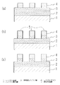
図1は、この発明の実施の形態1による半導体装置の製造方法を説明するための工程図である。この実施の形態1では、ドライエッチング反応生成物のみが除去され、レジストマスクが除去されぬように、薬液が選択される。
図1(a)は第1回目ドライエッチング開始前、図1(b)は第1回目ドライエッチング終了時、図1(c)は第1回目ウエットエッチング終了時の状態を示す模式的断面図である。
【0015】
まず図1(a)を参照して、シリコン基板1の表面上に膜厚が例えば1000nmのシリコン酸化膜2(SiO2)を熱酸化法で形成し、このシリコン酸化膜2上に例えば配線電極材料となる多結晶シリコン膜3を化学的気相成長(CVD)法で300nm堆積する。さらに多結晶シリコン膜3上にフォトレジストを約1000nmの厚さに回転塗布し、それをフオトリソグラフィ−(露光・現像)技術により配線電極のエッチングマスクとなるようにレジストマスク4をパタ−ニングする。
【0016】
ここでレジストマスク4は、例えばポジ型化学増幅レジスト材料(レプレ−社製、XP8843)、またはフォトレジスト(東京応化社製、OMR−83)を用いることができる。
なお、ドライエッチング処理されるためにレジストパターンが施される前の半導体ウェーハの状態は、図1(a)に示されるものに限らないが、これらを半導体試料と総称することにする。
【0017】
次に、図1(a)の半導体ウェーハは、図示しない反応性イオンエッチング(RIE)真空設備に装着されて、レジストマスク4をマスクとして多結晶シリコン膜3の第1回目(異方性)ドライエッチングが行われる。
ドライエッチング用の反応ガスは、ハロゲン系の臭化水素ガスHBrと塩素ガスCl2 ガスの混合ガスに酸素ガスO2が添加されている。酸素ガスが添加された場合は、シリコンとの反応生成物SiBrY の再分解物として
SiBr4 +O2 →SiO2 +2Br2
のように追加的に生成されるSiO2がレジストマスク4上に付着するのでレジストマスク4のエッチングが抑制される。その結果、レジストマスク4に対する多結晶シリコン膜3のエッチング選択比が格段に向上する。
【0018】
反応性ガスによるドライエッチングの工程で、シリコン反応としてのSiCl4 ,SiBrX と、酸化反応としてのSiOXと、レジストその他の有機物との有機反応としてのCを主成分としH,O,Nを含む有機物などの生成が進行し、これらが反応生成物5として半導体ウェーハに堆積し始める。この反応生成物5は、主にレジストマスク4と多結晶シリコン膜3の側面壁の表面上に残渣となって堆積する。その後、ドライエッチングは、図1(b)に示すように、シリコン酸化膜2が露出するタイミングで終了するように制御される。
【0019】
次に図1(b)の半導体ウェーハは、図示しないエッチング用化学設備に移されて、半導体ウェーハ上に堆積した不要な反応生成物5を除去するために、第1回目のウエットエッチングが行われる。このウエットエッチングでは、半導体ウェーハが、容積混合比で硫酸6:フッ酸1/600の混合液に、液温25℃で、6分間浸漬される。
【0020】
この薬液を用いたウエットエッチング工程によれば、図1(c)に示すように、レジストマスク4や多結晶シリコン膜3の側面壁などの表面上に残渣となって堆積していた反応生成物5のみが除去され、レジストマスク4は除去されず所望の状態でそのまま残る。このレジストマスク4は、後に続く工程で第2回目のウエットエッチングのマスクとして再使用することができる。
【0021】
なお、反応生成物5のうち、SiO2を主成分としSiXBrYなどを含む酸化膜系およびシリコン系のものは、フッ酸と反応して溶解除去される。また反応生成物5のうち、Cを主成分としH,O,Nなどを含む有機物系のものは、硫酸と反応して溶解除去される。
【0022】
レジストマスク4上のSiO2系の反応生成物5による保護効果もあるため、液温が常温の場合はレジストマスク4が溶解されることはないが、マスクとして再使用に支障が起こらないようにするために、液温は70℃以下に抑えることが望ましい。
【0023】
この実施の形態1における薬液の適切な混合比を選択するために、ドライエッチング反応生成物のみが除去され、レジストマスクが除去されぬように、図1(b)〜(c)において、硫酸:フッ酸の混合比を広範囲に変化させて実験を繰返した。
例えば赤外特性吸収帯の観測から有機系反応生成物を同定するなど各種の測定方法を併用して、試料ウェーハの表面状態を評価した。
【0024】
それらの実験結果から、液温の温度範囲が常温(例えば25℃)〜70℃の場合に、容積混合比として硫酸5〜7:フッ酸1/400〜1/1000の範囲で望ましい結果の得られることが分かった。以下この薬液を第1の薬液と呼称する。また、容積混合比として硫酸6:フッ酸1/400〜1/1000の範囲で最も望ましい結果の得られることが分かった
【0025】
第1の薬液において、硫酸5〜7に対してフッ酸の容積比が1/1000より、特に1/1500より低くなると、反応生成物5のうちSiO2を主体とする酸化膜系反応生成物の除去性が悪くなり、浸漬必要時間が所定の許容時間を超えて長くなり過ぎる。また、フッ酸の比が1/400より、特に1/300より高くなるとウェーハ表面の鏡面性が損なわれ、品質許容限界を超えるなどの理由から、第1の薬液の許容範囲が定められた。
【0026】
以上説明したように、この実施の形態1によれば、半導体ウェーハなど半導体試料から、不要なドライエッチング反応生成物のみが除去され、レジストマスクが除去されぬように、効果的な薬液処理をすることができる。
また、反応が連続又は同時に行われることにより、薬液及び処理時間の削減を図ることが可能である。
【0027】
実施の形態2.
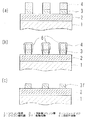
図2はこの発明の実施の形態2による半導体装置の製造方法を説明するための工程図である。この実施の形態2では、ドライエッチング反応生成物とともにレジストマスクも除去されるように薬液が選択される。
図2(a)は第2回目ドライエッチング開始前,図2(b)は第2回目ドライエッチング終了時,図2(c)は第2回目ウエットエッチング終了時の状態を示す模式的断面図である。
【0028】
第2回目ドライエッチング開始前を示す図2(a)は、図1(c)の半導体ウェーハが、図示しないRIE真空設備に移された状態を表している。ここでマスク4を第2回目のマスクとして、多結晶シリコン膜3に対する等方性ドライエッチングが開始される。第2回目のドライエッチング用の反応ガスとしては、実施の形態1で用いたガスと同一のHBrとCl2の混合ガスで、酸素ガスは添加されない。
【0029】
反応性ガスによるドライエッチングの工程で、シリコン反応としてのSiCl4 ,SiBrXと、酸化反応としてのSiOXと、レジストその他の有機物との有機反応としてのCを主成分としH,O,Nを含む有機物などの生成が進行し、これらが反応生成物6として半導体ウェーハに堆積し始める。この反応生成物6は、レジストマスク4や多結晶シリコン膜3の側面壁などの表面上に残渣となって堆積する。その後、ドライエッチングは、図2(b)に示すように、多結晶シリコン膜3の幅が所望量減少したところで終了するように制御される。
【0030】
次に図2(b)の半導体ウェーハは、図示しないエッチング用化学設備に移されて、半導体ウェーハ上に堆積した不要な反応生成物6を除去し、かつレジストマスク4も除去するために、第2回目のウエットエッチングが行われる。このウエットエッチングでは、半導体ウェーハが、容積混合比で、硫酸6:過酸化水素水1:フッ酸1/600の混合液に、液温100℃で、2分間浸漬される。
【0031】
図2(b)のレジストマスク4や多結晶シリコン膜3の側面壁などの表面上に残渣となって堆積していた反応生成物6と、レジストマスク4とは、ともに同時に、薬液への一度の浸漬工程によって除去されて、図2(c)に示すように、配線電極3fに不要な反応生成物が付着しない所望の状態が得られる。
【0032】
混合液中の過酸化水素水の作用により、反応生成物6のうちの有機系反応生成物やレジストマスク4の酸化が促進され、この酸化された後の有機系反応物やレジストマスク4は有機物に対して強い還元作用をもつ硫酸によって効果的に溶解除去される。また反応生成物6のうちの酸化膜系やシリコン系の反応生成物は、過酸化水素水の作用により酸化促進されフッ酸によって溶解除去される。溶解除去に必要な浸漬時間は液温の低下とともに増加するので、液温は70℃以上に保持することが望ましい。
【0033】
この実施の形態2における薬液の適切な混合比を選択するために、ドライエッチング反応生成物とともにレジストマスクが除去されるように、図2(b)〜(c)において、硫酸:過酸化水素水:フッ酸の混合比を広範囲に変化させて実験を繰返した。試料ウェーハ上の有機系など各種の反応生成物の同定や表面状態評価法は実施の形態1における方法と同じである。
【0034】
それらの実験結果から、液温の温度範囲が70〜100℃の場合に、容積混合比で硫酸5〜7:過酸化水素水1:フッ酸1/400〜1/1000の範囲で望ましい結果の得られることが分かった。以下この薬液を第2の薬液と呼称する。また、容積混合比で硫酸6:過酸化水素水1:フッ酸1/400〜1/1000の範囲で最も望ましい結果の得られることが分かった。
【0035】
第2の薬液において、過酸化水素水1に対して硫酸の容積比が5〜7より低くなると、レジストマスクの除去性が悪くなり、浸漬必要時間が所定の許容時間を超えて長くなり過ぎる。また、硫酸の容積比が7より高くなると、レジストマスクの除去性はよくなるが、酸化膜系反応生成物6の除去性が悪くなって、やはり浸漬必要時間が所定の許容時間を超えて長くなり過ぎる。
【0036】
また第2の薬液において、過酸化水素水1に対してフッ酸の容積比が1/1000より、特に1/1500より低くなると、反応生成物6のうちSiO2を主体とする酸化膜系反応生成物の除去性が悪くなり、浸漬必要時間が所定の許容時間を超えて長くなり過ぎる。また、フッ酸の比が1/400より、特に1/300より高くなるとウェーハ表面の鏡面性が損なわれ、品質許容限界を超えるなどの理由から、第2の薬液の許容範囲が定められた。
【0037】
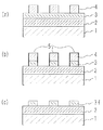
次に、図3は、実施の形態2によるエッチング方法を適用した他の事例を説明するための工程図である。図3(a)はドライエッチング開始前,図3(b)はドライエッチング終了時,図3(c)はウエットエッチング終了時の状態を示す模式的断面図である。
【0038】
図3(a)〜(b)の工程は、実施の形態1の図1(a)〜(b)と同様であるから、詳細な説明は省略する。
次に図3(b)の半導体ウェーハは、図示しないエッチング用化学設備に移されて、半導体ウェーハ上に堆積した不要な反応生成物5を除去し、かつレジストマスク4も除去するために、ウエットエッチングが行われる。この工程は、実施の形態2の図2(b)〜(c)と同様であるから詳細な説明は省略する。
この結果、図3(c)に示すように、配線電極3fに不要な反応生成物が付着しない所望の状態が得られる。
【0039】
以上説明したように、この実施の形態2によれば、半導体ウェーハなど半導体試料から、不要なドライエッチング反応生成物を除去するとともに、次の工程で用いないレジストマスクを同時に除去するように、効果的な薬液処理をすることができる。
また、反応が連続又は同時に行われることにより、薬液及び処理時間の削減を図ることが可能である。
【0040】
次に、実施の形態1〜2で説明したようなウエットエッチング工程の選択切替が可能な半導体装置の製造システムについて説明する。
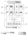
図4は、被エッチング層のエッチング要求に対応して、薬液またはウエットエッチング工程の選択切替が可能な製造システムを説明するための図である。
【0041】
図4において、11はドライエッチング用真空設備、21はウエットエッチング用化学設備、22は化学設備の薬液やウエットエッチング工程を制御する制御装置である。第1の薬液槽23と24、第2の薬液槽25と26のように、異なる薬液毎に各々複数槽が用意され、そして例えば同じ薬液の2槽は各々異なる液温に保持されている。
【0042】
制御装置22は、到来した半導体ウェーハの被エッチング層のエッチング要求に対応して、薬液またはウエットエッチング工程の選択切替が可能で、また薬液の種類を選択した後、エッチング要求に最適の液温に保持されている薬液槽が選択されるように制御可能に構成されている。
【0043】
実施の形態1〜2において上述したように、ウエットエッチングによって、不要な反応生成物だけを除去するか、レジストマスクを反応生成物とともに除去するか、いずれにするかは被エッチング層のエッチング要求によって決められる。しかし半導体ウェーハ上に各種の成膜を積層し、順次それらの成膜をエッチング、洗浄する工程が繰返される半導体装置の製造システムにおいては、ウエットエッチング工程とその薬液に限定したとしても、実施の形態1〜2で開示された以外に選択切替すべき条件は多種多様である。図3のウエットエッチング工程の選択切替が可能な製造システムはその一例である。
【0044】
以上、ドライエッチングの被エッチング層としては、実施の形態1〜2において多結晶シリコンを具体例として述べたがこれに限定されず、例えばMOS−FETのゲ−トとなる薄膜の多結晶シリコンや、または、単結晶シリコン、アモルフアスシリコン、シリサイド、ポリサイド、酸化シリコン、窒化シリコン、または酸化窒化シリコンのいずれかを主成分とする材料であってもよい。またGaAsなどのIII−V族化合物半導体の材料を含んでいてもよい。
【0045】
また、ドライエッチング用の反応ガスは、実施の形態1および2において臭化水素HBr、臭素Br2、塩素ガスCl2について述べたがこれに限定されず、例えばフッ素系ガスCF4 、CHF3 、CH2F2 、またはC2F6のうちから選択されてもよい。
【0046】
第1の薬液または第2の薬液によって除去される反応生成物はSiO2、SiXBrY,CXFYSiZを主成分とするシリコン系材料およびCを主成分としH,O,Nを含む有機系材料であってもよい。
【0047】
【発明の効果】
この発明によれば、ドライエッチングで生成され半導体試料に付着した反応生成物を、硫酸とフッ酸とを含む薬液により洗浄して除去するので、成膜時または成膜後に平坦性の悪化やエッチング不良などを引起こすことを防止できる効果がある。
【0048】
また、この発明によれば、ドライエッチングで生成され半導体試料に付着した反応生成物とレジストパターンとを、硫酸と過酸化水素水とフッ酸とを含む薬液によりエッチング除去するので、成膜時または成膜後に平坦性の悪化やエッチング不良などを引起こすことを防止できる効果がある。
【図面の簡単な説明】
【図1】この発明の実施の形態1による半導体装置の製造方法を説明するための工程図である。
【図2】この発明の実施の形態2による半導体装置の製造方法を説明するための工程図である。
【図3】この発明の実施の形態2による半導体装置の製造方法を説明するための他の工程図である。
【図4】この発明の実施の形態1〜2による半導体装置の製造方法を実施するめの半導体製造システムを説明するための図である。
【符号の説明】
1 シリコン基板、2 シリコン酸化膜、3 多結晶シリコン膜、3f配線電極、4 レジストマスク、5,6 反応生成物。[0001]
BACKGROUND OF THE INVENTION
The present invention relates to a method of manufacturing a semiconductor device including a wet etching step for removing a reaction product generated by dry etching from a semiconductor wafer, or simultaneously removing a reaction product and a resist mask, and a semiconductor by the manufacturing method. It relates to the device.
[0002]
[Prior art]
As a conventional technique, for example, Japanese Laid-Open Patent Publication No. 49-10746 discloses a method of cleaning a silicon wafer with a mixed solution of sulfuric acid, hydrogen peroxide solution, and hydrofluoric acid. However, a reaction generated by dry etching is disclosed. Techniques for removing the product and resist mask are not shown.
[0003]
For techniques for removing a reaction product and a resist mask generated by dry etching of a silicon oxide film or a polycrystalline silicon film on a silicon substrate, see A: JP-A-4-142741, B: JP-A. 7-99178, C: disclosed in JP-A-8-339996. In particular, “I” relates to a adhered particle, “B” relates to a dry etching damage layer, and “C” relates to a technique for removing minute foreign matters by wet etching. In other words, “I” is sulfuric acid / hydrogen peroxide solution → pure water → hydrogen peroxide solution / ammonia → pure water, “B” is hydrofluoric acid → sulfuric acid / hydrogen peroxide solution → hydrofluoric acid, and “ha” is buffered ammonium fluoride. Wet etching techniques such as solution → sulfuric acid / hydrogen peroxide solution → hydrofluoric acid → pure water are disclosed.
[0004]
As described above, conventionally, removal has been performed separately for each material to be etched such as organic, silicon, and oxide films, or for each type of object to be removed, using a corresponding chemical solution. Therefore, there are many types and amounts of chemicals used, multi-tank processing in which the chemicals are immersed in different chemicals sequentially, so the number of processes is long and the processing time is long, and the equipment used for the vacuum equipment for dry etching and chemical equipment for wet etching. The production and quality control was complicated because it was necessary to switch over many times.
[0005]
Conventionally, a method of removing only various reaction products by leaving a resist mask for continuous use by a single chemical solution or wet etching process, or an appropriate method of simultaneously removing various reaction products together with a resist mask. There was no need to establish it.
[0006]
[Problems to be solved by the invention]
The present invention has been made to solve the above-described problems, and an object of the present invention is to provide a semiconductor device capable of removing only a reaction product by dry etching or a reaction product and a resist mask with a small amount of chemical solution. A manufacturing method is to be provided.
[0007]
[Means for Solving the Problems]
[0009]
The method of manufacturing a semiconductor device according to
[0010]
In the method of manufacturing a semiconductor device according to
[0011]
According to a third aspect of the present invention, there is provided a method of manufacturing a semiconductor device, wherein a step of etching and removing with the chemical solution is performed following the step of dry etching .
[0014]
DETAILED DESCRIPTION OF THE INVENTION
Hereinafter, embodiments of the present invention will be described with reference to FIGS. In the drawings, the same reference numerals denote the same or corresponding parts.
1A to 1D are process diagrams for explaining a semiconductor device manufacturing method according to the first embodiment of the present invention. In the first embodiment, the chemical solution is selected so that only the dry etching reaction product is removed and the resist mask is not removed.
FIG. 1A is a schematic cross-sectional view showing a state before the start of the first dry etching, FIG. 1B is a state at the end of the first dry etching, and FIG. 1C is a state at the end of the first wet etching. is there.
[0015]
First, referring to FIG. 1A, a silicon oxide film 2 (SiO 2 ) having a film thickness of, for example, 1000 nm is formed on the surface of a
[0016]
Here, as the
The state of the semiconductor wafer before the resist pattern is applied for the dry etching process is not limited to that shown in FIG. 1A, but these are collectively referred to as a semiconductor sample.
[0017]
Next, the semiconductor wafer of FIG. 1A is mounted in a reactive ion etching (RIE) vacuum facility (not shown), and the first (anisotropic) dry of the
As a reactive gas for dry etching, oxygen gas O 2 is added to a mixed gas of halogen-based hydrogen bromide gas HBr and chlorine gas Cl 2 gas. When oxygen gas is added, SiBr 4 + O 2 → SiO 2 + 2Br 2 as a re-decomposition product of the reaction product SiBr Y with silicon.
Since the additionally generated SiO 2 adheres on the
[0018]
In the process of dry etching with a reactive gas, SiCl 4 and SiBr X as a silicon reaction, SiO X as an oxidation reaction, and C as an organic reaction with a resist and other organic substances as main components, H, O, and N Production of organic substances and the like that are contained proceeds, and these start to be deposited as
[0019]
Next, the semiconductor wafer of FIG. 1B is transferred to an etching chemical facility (not shown), and a first wet etching is performed to remove
[0020]
According to the wet etching process using this chemical solution, as shown in FIG. 1C, the reaction product deposited as a residue on the surface of the resist
[0021]
Of the
[0022]
Since there is also a protective effect by the SiO 2 -based
[0023]
In order to select an appropriate mixing ratio of the chemicals in the first embodiment, in FIG. 1B to FIG. 1C, only the dry etching reaction product is removed and the resist mask is not removed. The experiment was repeated with the mixture ratio of hydrofluoric acid varied widely.
For example, the surface state of the sample wafer was evaluated by using various measurement methods such as identifying an organic reaction product from observation of an infrared characteristic absorption band.
[0024]
From these experimental results, when the temperature range of the liquid temperature is from room temperature (for example, 25 ° C.) to 70 ° C., a desired result is obtained when the volume mixing ratio is sulfuric acid 5-7:
In the first chemical solution, when the volume ratio of hydrofluoric acid to
[0026]
As described above, according to the first embodiment, an effective chemical treatment is performed so that only unnecessary dry etching reaction products are removed from the semiconductor sample such as a semiconductor wafer and the resist mask is not removed. be able to.
Moreover, it is possible to aim at reduction of a chemical | medical solution and processing time by performing reaction continuously or simultaneously.
[0027]
FIG. 2 is a process diagram for explaining the method of manufacturing a semiconductor device according to the second embodiment of the present invention. In the second embodiment, the chemical solution is selected so that the resist mask is removed together with the dry etching reaction product.
2A is a schematic cross-sectional view showing a state before the start of the second dry etching, FIG. 2B is a schematic cross-sectional view showing a state at the end of the second dry etching, and FIG. 2C is a state at the end of the second wet etching. is there.
[0028]
FIG. 2A showing the start of the second dry etching shows a state in which the semiconductor wafer of FIG. 1C has been transferred to an RIE vacuum facility (not shown). Here, isotropic dry etching of the
[0029]
In the process of dry etching with a reactive gas, SiCl 4 and SiBr X as a silicon reaction, SiO X as an oxidation reaction, and C as an organic reaction with a resist and other organic substances as main components, H, O, and N Production of organic substances and the like that are contained proceeds, and these start to be deposited on the semiconductor wafer as
[0030]
Next, the semiconductor wafer of FIG. 2B is moved to an etching chemical facility (not shown), and the
[0031]
The
[0032]
Oxidation of the organic reaction product of the
[0033]
In order to select an appropriate mixing ratio of the chemicals in the second embodiment, sulfuric acid: hydrogen peroxide solution is used in FIGS. 2B to 2C so that the resist mask is removed together with the dry etching reaction product. : The experiment was repeated by changing the mixing ratio of hydrofluoric acid over a wide range. The identification of various reaction products such as organic systems on the sample wafer and the surface state evaluation method are the same as those in the first embodiment.
[0034]
From these experimental results, when the temperature range of the liquid temperature is 70 to 100 ° C., desirable results are obtained in the range of
[0035]
In the second chemical solution, when the volume ratio of sulfuric acid to the
[0036]
Further, in the second chemical solution, when the volume ratio of hydrofluoric acid to the
[0037]
Next, FIG. 3 is a process diagram for explaining another example to which the etching method according to the second embodiment is applied. 3A is a schematic cross-sectional view showing a state before dry etching is started, FIG. 3B is a state when dry etching is finished, and FIG. 3C is a state when wet etching is finished.
[0038]
3A to 3B are the same as those in FIGS. 1A to 1B of the first embodiment, and detailed description thereof is omitted.
Next, the semiconductor wafer shown in FIG. 3B is transferred to an etching chemical facility (not shown) to remove
As a result, as shown in FIG. 3C, a desired state in which unnecessary reaction products do not adhere to the
[0039]
As described above, according to the second embodiment, it is possible to remove unnecessary dry etching reaction products from a semiconductor sample such as a semiconductor wafer and simultaneously remove a resist mask that is not used in the next step. The chemical solution can be processed.
Moreover, it is possible to aim at reduction of a chemical | medical solution and processing time by performing reaction continuously or simultaneously.
[0040]
Next, a semiconductor device manufacturing system capable of selecting and switching the wet etching process as described in the first and second embodiments will be described.
FIG. 4 is a diagram for explaining a manufacturing system capable of selectively switching a chemical solution or a wet etching process in response to an etching request for a layer to be etched.
[0041]
In FIG. 4, 11 is a vacuum equipment for dry etching, 21 is a chemical equipment for wet etching, and 22 is a control device for controlling chemical solutions and wet etching processes in the chemical equipment. Like the 1st chemical |
[0042]
The
[0043]
As described above in the first and second embodiments, only the unnecessary reaction product is removed by wet etching, or the resist mask is removed together with the reaction product, depending on the etching requirement of the etching target layer. It is decided. However, in a semiconductor device manufacturing system in which various film formations are stacked on a semiconductor wafer, and the process of sequentially etching and cleaning these film formations is repeated, even if limited to the wet etching process and its chemical solution, the embodiment Various conditions other than those disclosed in 1-2 are to be selected and switched. The manufacturing system capable of selectively switching the wet etching process in FIG. 3 is an example.
[0044]
As described above, the polycrystalline silicon has been described as a specific example in the first and second embodiments as the layer to be etched by dry etching. However, the present invention is not limited to this. For example, a thin film of polycrystalline silicon serving as a gate of a MOS-FET, Alternatively, a material mainly containing any of single crystal silicon, amorphous silicon, silicide, polycide, silicon oxide, silicon nitride, or silicon oxynitride may be used. Further, it may contain a III-V group compound semiconductor material such as GaAs.
[0045]
In addition, as the reactive gas for dry etching, hydrogen bromide HBr, bromine Br 2 , and chlorine gas Cl 2 are described in the first and second embodiments, but the present invention is not limited thereto. For example, fluorine-based gases CF 4 , CHF 3 , It may be selected from CH 2 F 2 or C 2 F 6 .
[0046]
The reaction product removed by the first chemical solution or the second chemical solution is a silicon-based material whose main component is SiO 2 , Si X Br Y , C X F Y Si Z , and H, O, N whose main component is C. It may be an organic material containing
[0047]
【The invention's effect】
According to the present invention, reaction products generated by dry etching and adhering to a semiconductor sample are removed by washing with a chemical solution containing sulfuric acid and hydrofluoric acid. This has the effect of preventing the occurrence of defects.
[0048]
Further, according to the present invention, the reaction product and the resist pattern generated by dry etching and adhering to the semiconductor sample are removed by etching with a chemical solution containing sulfuric acid, hydrogen peroxide solution, and hydrofluoric acid. There is an effect that it is possible to prevent deterioration of flatness and poor etching after film formation.
[Brief description of the drawings]
FIG. 1 is a process diagram for explaining a method of manufacturing a semiconductor device according to a first embodiment of the present invention.
FIG. 2 is a process diagram for describing the manufacturing method of the semiconductor device according to the second embodiment of the present invention;
FIG. 3 is another process diagram for explaining the method for manufacturing a semiconductor device according to the second embodiment of the present invention;
FIG. 4 is a diagram for explaining a semiconductor manufacturing system for carrying out a semiconductor device manufacturing method according to first and second embodiments of the present invention;
[Explanation of symbols]
1 silicon substrate, 2 silicon oxide film, 3 polycrystalline silicon film, 3f wiring electrode, 4 resist mask, 5 and 6 reaction product.
Claims (3)
Priority Applications (5)
| Application Number | Priority Date | Filing Date | Title |
|---|---|---|---|
| JP29716797A JP3607061B2 (en) | 1997-10-29 | 1997-10-29 | Manufacturing method of semiconductor device |
| US09/070,914 US6110834A (en) | 1997-10-29 | 1998-05-04 | Semiconductor device and manufacturing method thereof for removing reaction products of dry etching |
| TW087110453A TW511183B (en) | 1997-10-29 | 1998-06-29 | Manufacturing method of semiconductor device and semiconductor device |
| KR1019980026448A KR19990036549A (en) | 1997-10-29 | 1998-07-01 | Semiconductor device manufacturing method and semiconductor device |
| DE19829863A DE19829863B4 (en) | 1997-10-29 | 1998-07-03 | Method for producing a semiconductor device |
Applications Claiming Priority (1)
| Application Number | Priority Date | Filing Date | Title |
|---|---|---|---|
| JP29716797A JP3607061B2 (en) | 1997-10-29 | 1997-10-29 | Manufacturing method of semiconductor device |
Publications (2)
| Publication Number | Publication Date |
|---|---|
| JPH11135473A JPH11135473A (en) | 1999-05-21 |
| JP3607061B2 true JP3607061B2 (en) | 2005-01-05 |
Family
ID=17843063
Family Applications (1)
| Application Number | Title | Priority Date | Filing Date |
|---|---|---|---|
| JP29716797A Expired - Fee Related JP3607061B2 (en) | 1997-10-29 | 1997-10-29 | Manufacturing method of semiconductor device |
Country Status (5)
| Country | Link |
|---|---|
| US (1) | US6110834A (en) |
| JP (1) | JP3607061B2 (en) |
| KR (1) | KR19990036549A (en) |
| DE (1) | DE19829863B4 (en) |
| TW (1) | TW511183B (en) |
Families Citing this family (13)
| Publication number | Priority date | Publication date | Assignee | Title |
|---|---|---|---|---|
| TW589685B (en) * | 2000-07-14 | 2004-06-01 | Infineon Technologies Corp | Etching composition and use thereof with feedback control of HF in BEOL clean |
| JP2002353205A (en) * | 2000-08-28 | 2002-12-06 | Mitsubishi Electric Corp | Semiconductor device manufacturing method, wafer processing apparatus used therefor, and semiconductor device |
| JP3889271B2 (en) | 2000-12-15 | 2007-03-07 | 株式会社東芝 | Manufacturing method of semiconductor device |
| CA2413666A1 (en) * | 2002-03-26 | 2003-09-26 | Takayuki Homma | Charge-giving body, and pattern-formed body using the same |
| TWI229917B (en) * | 2003-09-09 | 2005-03-21 | Nanya Technology Corp | Interconnect process and method for removing silicide |
| JP2005167181A (en) * | 2003-11-10 | 2005-06-23 | Daikin Ind Ltd | Etching solution for low-k film and etching method |
| JP4326928B2 (en) * | 2003-12-09 | 2009-09-09 | 株式会社東芝 | Composition for removing photoresist residue and method for producing semiconductor circuit element using the composition |
| JP4642001B2 (en) | 2006-10-24 | 2011-03-02 | 関東化学株式会社 | Composition for removing photoresist residue and polymer residue |
| JP2008270824A (en) * | 2008-05-09 | 2008-11-06 | Renesas Technology Corp | Method for manufacturing semiconductor device |
| CN102468131B (en) * | 2010-11-10 | 2016-06-01 | 中国科学院微电子研究所 | Polymer Removal Method after Etching of High K Gate Dielectric/Metal Gate Stacked Gate Structure |
| US8334205B2 (en) | 2010-11-10 | 2012-12-18 | Institute of Microelectronics, Chinese Academy of Sciences | Method for removing polymer after etching gate stack structure of high-K gate dielectric/metal gate |
| JP6026375B2 (en) | 2013-09-02 | 2016-11-16 | 株式会社東芝 | Manufacturing method of semiconductor device |
| CN114038942A (en) * | 2021-11-08 | 2022-02-11 | 浙江光特科技有限公司 | Etching photoresist removing method for photoelectric detector chip |
Family Cites Families (14)
| Publication number | Priority date | Publication date | Assignee | Title |
|---|---|---|---|---|
| JPS5922380B2 (en) * | 1975-12-03 | 1984-05-26 | 株式会社東芝 | Handout Taisoshino Seizouhouhou |
| JPS5923106B2 (en) * | 1976-10-13 | 1984-05-30 | 日本電気株式会社 | Manufacturing method of semiconductor device |
| JPS5830135A (en) * | 1981-08-17 | 1983-02-22 | Toshiba Corp | Method of cleaning semiconductor wafer |
| US4585515A (en) * | 1985-03-11 | 1986-04-29 | Rca Corporation | Formation of conductive lines |
| US5443998A (en) * | 1989-08-01 | 1995-08-22 | Cypress Semiconductor Corp. | Method of forming a chlorinated silicon nitride barrier layer |
| JPH03218629A (en) * | 1989-11-22 | 1991-09-26 | Fujitsu Ltd | Cleaning of semiconductor substrate |
| JP2787788B2 (en) * | 1990-09-26 | 1998-08-20 | インターナショナル・ビジネス・マシーンズ・コーポレーション | Residue removal method |
| JPH04142741A (en) * | 1990-10-04 | 1992-05-15 | Nec Corp | Semiconductor manufacturing device |
| KR0124484B1 (en) * | 1993-03-23 | 1997-12-10 | 모리시다 요이치 | A method and apparatus for cleaning the semiconductor device |
| JPH0799178A (en) * | 1993-09-28 | 1995-04-11 | Fujitsu Ltd | Method for manufacturing semiconductor device |
| TW347597B (en) * | 1994-01-31 | 1998-12-11 | Mitsubishi Chem Corp | Method of forming a groove in a semiconductor laser diode and a semiconductor laser diode |
| JPH08250400A (en) * | 1995-03-14 | 1996-09-27 | Mitsubishi Electric Corp | Silicone resin removal method |
| JPH08339996A (en) * | 1995-06-12 | 1996-12-24 | Toshiba Corp | Method for manufacturing semiconductor device |
| TW296405B (en) * | 1996-02-12 | 1997-01-21 | Merck Kanto Advanced Chemical | Solution and process for removing side-wall residue after dry etching |
-
1997
- 1997-10-29 JP JP29716797A patent/JP3607061B2/en not_active Expired - Fee Related
-
1998
- 1998-05-04 US US09/070,914 patent/US6110834A/en not_active Expired - Lifetime
- 1998-06-29 TW TW087110453A patent/TW511183B/en not_active IP Right Cessation
- 1998-07-01 KR KR1019980026448A patent/KR19990036549A/en not_active Ceased
- 1998-07-03 DE DE19829863A patent/DE19829863B4/en not_active Expired - Fee Related
Also Published As
| Publication number | Publication date |
|---|---|
| DE19829863A1 (en) | 1999-05-06 |
| JPH11135473A (en) | 1999-05-21 |
| TW511183B (en) | 2002-11-21 |
| KR19990036549A (en) | 1999-05-25 |
| DE19829863B4 (en) | 2006-06-29 |
| US6110834A (en) | 2000-08-29 |
Similar Documents
| Publication | Publication Date | Title |
|---|---|---|
| JP2731750B2 (en) | Etching residue removal method | |
| JP3607061B2 (en) | Manufacturing method of semiconductor device | |
| JP2000311899A (en) | Method for manufacturing semiconductor device | |
| US6283131B1 (en) | In-situ strip process for polysilicon etching in deep sub-micron technology | |
| JPH0621018A (en) | Dry etching method | |
| US7442652B2 (en) | Method for removing contamination and method for fabricating semiconductor device | |
| US7307009B2 (en) | Phosphoric acid free process for polysilicon gate definition | |
| JP2009081247A (en) | Ruthenium film etching method | |
| US6605230B1 (en) | Solutions and processes for removal of sidewall residue after dry etching | |
| US5387312A (en) | High selective nitride etch | |
| KR20060039314A (en) | Cleaning solution and method for cleaning semiconductor device using same | |
| US5989979A (en) | Method for controlling the silicon nitride profile during patterning using a novel plasma etch process | |
| US6296988B1 (en) | Method for forming a mental wiring pattern on a semiconductor device | |
| JP2003520446A (en) | Residue removal method that prevents oxide from being etched | |
| JP2003179064A (en) | Wiring pattern forming method | |
| JP2001102369A (en) | Resist removal method | |
| JPS639121A (en) | Dry etching | |
| JPH06310468A (en) | Dry etching method | |
| JP3487734B2 (en) | Pattern formation method | |
| JPH0794469A (en) | Dry etching method | |
| CN114203546B (en) | Semiconductor devices and their manufacturing methods | |
| JPH07321091A (en) | Etching and wiring forming method | |
| US6727166B1 (en) | Removal of silicon oxynitride material using a wet chemical process after gate etch processing | |
| JP3740792B2 (en) | Manufacturing method of semiconductor device | |
| JPH05217961A (en) | Precision processing method of silicon |
Legal Events
| Date | Code | Title | Description |
|---|---|---|---|
| A131 | Notification of reasons for refusal |
Free format text: JAPANESE INTERMEDIATE CODE: A131 Effective date: 20040713 |
|
| A521 | Request for written amendment filed |
Free format text: JAPANESE INTERMEDIATE CODE: A523 Effective date: 20040902 |
|
| TRDD | Decision of grant or rejection written | ||
| A01 | Written decision to grant a patent or to grant a registration (utility model) |
Free format text: JAPANESE INTERMEDIATE CODE: A01 Effective date: 20041005 |
|
| A61 | First payment of annual fees (during grant procedure) |
Free format text: JAPANESE INTERMEDIATE CODE: A61 Effective date: 20041006 |
|
| R150 | Certificate of patent or registration of utility model |
Free format text: JAPANESE INTERMEDIATE CODE: R150 |
|
| FPAY | Renewal fee payment (event date is renewal date of database) |
Free format text: PAYMENT UNTIL: 20081015 Year of fee payment: 4 |
|
| FPAY | Renewal fee payment (event date is renewal date of database) |
Free format text: PAYMENT UNTIL: 20081015 Year of fee payment: 4 |
|
| FPAY | Renewal fee payment (event date is renewal date of database) |
Free format text: PAYMENT UNTIL: 20091015 Year of fee payment: 5 |
|
| LAPS | Cancellation because of no payment of annual fees |