JP3600115B2 - High frequency circuit and communication system - Google Patents
High frequency circuit and communication system Download PDFInfo
- Publication number
- JP3600115B2 JP3600115B2 JP2000103784A JP2000103784A JP3600115B2 JP 3600115 B2 JP3600115 B2 JP 3600115B2 JP 2000103784 A JP2000103784 A JP 2000103784A JP 2000103784 A JP2000103784 A JP 2000103784A JP 3600115 B2 JP3600115 B2 JP 3600115B2
- Authority
- JP
- Japan
- Prior art keywords
- output
- cell block
- amplifier
- amplifier cell
- power
- Prior art date
- Legal status (The legal status is an assumption and is not a legal conclusion. Google has not performed a legal analysis and makes no representation as to the accuracy of the status listed.)
- Expired - Fee Related
Links
Images


Classifications
-
- H—ELECTRICITY
- H03—ELECTRONIC CIRCUITRY
- H03F—AMPLIFIERS
- H03F1/00—Details of amplifiers with only discharge tubes, only semiconductor devices or only unspecified devices as amplifying elements
- H03F1/02—Modifications of amplifiers to raise the efficiency, e.g. gliding Class A stages, use of an auxiliary oscillation
- H03F1/0205—Modifications of amplifiers to raise the efficiency, e.g. gliding Class A stages, use of an auxiliary oscillation in transistor amplifiers
- H03F1/0283—Reducing the number of Dc-current paths
-
- H—ELECTRICITY
- H01—ELECTRIC ELEMENTS
- H01P—WAVEGUIDES; RESONATORS, LINES, OR OTHER DEVICES OF THE WAVEGUIDE TYPE
- H01P5/00—Coupling devices of the waveguide type
- H01P5/08—Coupling devices of the waveguide type for linking dissimilar lines or devices
- H01P5/10—Coupling devices of the waveguide type for linking dissimilar lines or devices for coupling balanced with unbalanced lines or devices
- H01P5/107—Hollow-waveguide/strip-line transitions
-
- H—ELECTRICITY
- H01—ELECTRIC ELEMENTS
- H01L—SEMICONDUCTOR DEVICES NOT COVERED BY CLASS H10
- H01L24/00—Arrangements for connecting or disconnecting semiconductor or solid-state bodies; Methods or apparatus related thereto
- H01L24/01—Means for bonding being attached to, or being formed on, the surface to be connected, e.g. chip-to-package, die-attach, "first-level" interconnects; Manufacturing methods related thereto
- H01L24/42—Wire connectors; Manufacturing methods related thereto
- H01L24/47—Structure, shape, material or disposition of the wire connectors after the connecting process
- H01L24/49—Structure, shape, material or disposition of the wire connectors after the connecting process of a plurality of wire connectors
-
- H—ELECTRICITY
- H03—ELECTRONIC CIRCUITRY
- H03F—AMPLIFIERS
- H03F3/00—Amplifiers with only discharge tubes or only semiconductor devices as amplifying elements
- H03F3/72—Gated amplifiers, i.e. amplifiers which are rendered operative or inoperative by means of a control signal
-
- H—ELECTRICITY
- H01—ELECTRIC ELEMENTS
- H01L—SEMICONDUCTOR DEVICES NOT COVERED BY CLASS H10
- H01L2223/00—Details relating to semiconductor or other solid state devices covered by the group H01L23/00
- H01L2223/58—Structural electrical arrangements for semiconductor devices not otherwise provided for
- H01L2223/64—Impedance arrangements
- H01L2223/66—High-frequency adaptations
- H01L2223/6644—Packaging aspects of high-frequency amplifiers
-
- H—ELECTRICITY
- H01—ELECTRIC ELEMENTS
- H01L—SEMICONDUCTOR DEVICES NOT COVERED BY CLASS H10
- H01L2224/00—Indexing scheme for arrangements for connecting or disconnecting semiconductor or solid-state bodies and methods related thereto as covered by H01L24/00
- H01L2224/01—Means for bonding being attached to, or being formed on, the surface to be connected, e.g. chip-to-package, die-attach, "first-level" interconnects; Manufacturing methods related thereto
- H01L2224/42—Wire connectors; Manufacturing methods related thereto
- H01L2224/47—Structure, shape, material or disposition of the wire connectors after the connecting process
- H01L2224/48—Structure, shape, material or disposition of the wire connectors after the connecting process of an individual wire connector
- H01L2224/4805—Shape
- H01L2224/4809—Loop shape
- H01L2224/48091—Arched
-
- H—ELECTRICITY
- H01—ELECTRIC ELEMENTS
- H01L—SEMICONDUCTOR DEVICES NOT COVERED BY CLASS H10
- H01L2224/00—Indexing scheme for arrangements for connecting or disconnecting semiconductor or solid-state bodies and methods related thereto as covered by H01L24/00
- H01L2224/01—Means for bonding being attached to, or being formed on, the surface to be connected, e.g. chip-to-package, die-attach, "first-level" interconnects; Manufacturing methods related thereto
- H01L2224/42—Wire connectors; Manufacturing methods related thereto
- H01L2224/47—Structure, shape, material or disposition of the wire connectors after the connecting process
- H01L2224/49—Structure, shape, material or disposition of the wire connectors after the connecting process of a plurality of wire connectors
- H01L2224/491—Disposition
- H01L2224/4911—Disposition the connectors being bonded to at least one common bonding area, e.g. daisy chain
- H01L2224/49111—Disposition the connectors being bonded to at least one common bonding area, e.g. daisy chain the connectors connecting two common bonding areas, e.g. Litz or braid wires
-
- H—ELECTRICITY
- H01—ELECTRIC ELEMENTS
- H01L—SEMICONDUCTOR DEVICES NOT COVERED BY CLASS H10
- H01L2224/00—Indexing scheme for arrangements for connecting or disconnecting semiconductor or solid-state bodies and methods related thereto as covered by H01L24/00
- H01L2224/01—Means for bonding being attached to, or being formed on, the surface to be connected, e.g. chip-to-package, die-attach, "first-level" interconnects; Manufacturing methods related thereto
- H01L2224/42—Wire connectors; Manufacturing methods related thereto
- H01L2224/47—Structure, shape, material or disposition of the wire connectors after the connecting process
- H01L2224/49—Structure, shape, material or disposition of the wire connectors after the connecting process of a plurality of wire connectors
- H01L2224/491—Disposition
- H01L2224/4912—Layout
- H01L2224/49175—Parallel arrangements
-
- H—ELECTRICITY
- H01—ELECTRIC ELEMENTS
- H01L—SEMICONDUCTOR DEVICES NOT COVERED BY CLASS H10
- H01L24/00—Arrangements for connecting or disconnecting semiconductor or solid-state bodies; Methods or apparatus related thereto
- H01L24/01—Means for bonding being attached to, or being formed on, the surface to be connected, e.g. chip-to-package, die-attach, "first-level" interconnects; Manufacturing methods related thereto
- H01L24/42—Wire connectors; Manufacturing methods related thereto
- H01L24/47—Structure, shape, material or disposition of the wire connectors after the connecting process
- H01L24/48—Structure, shape, material or disposition of the wire connectors after the connecting process of an individual wire connector
-
- H—ELECTRICITY
- H01—ELECTRIC ELEMENTS
- H01L—SEMICONDUCTOR DEVICES NOT COVERED BY CLASS H10
- H01L2924/00—Indexing scheme for arrangements or methods for connecting or disconnecting semiconductor or solid-state bodies as covered by H01L24/00
- H01L2924/0001—Technical content checked by a classifier
- H01L2924/00014—Technical content checked by a classifier the subject-matter covered by the group, the symbol of which is combined with the symbol of this group, being disclosed without further technical details
-
- H—ELECTRICITY
- H01—ELECTRIC ELEMENTS
- H01L—SEMICONDUCTOR DEVICES NOT COVERED BY CLASS H10
- H01L2924/00—Indexing scheme for arrangements or methods for connecting or disconnecting semiconductor or solid-state bodies as covered by H01L24/00
- H01L2924/01—Chemical elements
- H01L2924/01004—Beryllium [Be]
-
- H—ELECTRICITY
- H01—ELECTRIC ELEMENTS
- H01L—SEMICONDUCTOR DEVICES NOT COVERED BY CLASS H10
- H01L2924/00—Indexing scheme for arrangements or methods for connecting or disconnecting semiconductor or solid-state bodies as covered by H01L24/00
- H01L2924/01—Chemical elements
- H01L2924/01005—Boron [B]
-
- H—ELECTRICITY
- H01—ELECTRIC ELEMENTS
- H01L—SEMICONDUCTOR DEVICES NOT COVERED BY CLASS H10
- H01L2924/00—Indexing scheme for arrangements or methods for connecting or disconnecting semiconductor or solid-state bodies as covered by H01L24/00
- H01L2924/01—Chemical elements
- H01L2924/01006—Carbon [C]
-
- H—ELECTRICITY
- H01—ELECTRIC ELEMENTS
- H01L—SEMICONDUCTOR DEVICES NOT COVERED BY CLASS H10
- H01L2924/00—Indexing scheme for arrangements or methods for connecting or disconnecting semiconductor or solid-state bodies as covered by H01L24/00
- H01L2924/01—Chemical elements
- H01L2924/01023—Vanadium [V]
-
- H—ELECTRICITY
- H01—ELECTRIC ELEMENTS
- H01L—SEMICONDUCTOR DEVICES NOT COVERED BY CLASS H10
- H01L2924/00—Indexing scheme for arrangements or methods for connecting or disconnecting semiconductor or solid-state bodies as covered by H01L24/00
- H01L2924/01—Chemical elements
- H01L2924/01027—Cobalt [Co]
-
- H—ELECTRICITY
- H01—ELECTRIC ELEMENTS
- H01L—SEMICONDUCTOR DEVICES NOT COVERED BY CLASS H10
- H01L2924/00—Indexing scheme for arrangements or methods for connecting or disconnecting semiconductor or solid-state bodies as covered by H01L24/00
- H01L2924/01—Chemical elements
- H01L2924/0105—Tin [Sn]
-
- H—ELECTRICITY
- H01—ELECTRIC ELEMENTS
- H01L—SEMICONDUCTOR DEVICES NOT COVERED BY CLASS H10
- H01L2924/00—Indexing scheme for arrangements or methods for connecting or disconnecting semiconductor or solid-state bodies as covered by H01L24/00
- H01L2924/10—Details of semiconductor or other solid state devices to be connected
- H01L2924/11—Device type
- H01L2924/13—Discrete devices, e.g. 3 terminal devices
- H01L2924/1304—Transistor
- H01L2924/1305—Bipolar Junction Transistor [BJT]
-
- H—ELECTRICITY
- H01—ELECTRIC ELEMENTS
- H01L—SEMICONDUCTOR DEVICES NOT COVERED BY CLASS H10
- H01L2924/00—Indexing scheme for arrangements or methods for connecting or disconnecting semiconductor or solid-state bodies as covered by H01L24/00
- H01L2924/10—Details of semiconductor or other solid state devices to be connected
- H01L2924/11—Device type
- H01L2924/13—Discrete devices, e.g. 3 terminal devices
- H01L2924/1304—Transistor
- H01L2924/1306—Field-effect transistor [FET]
-
- H—ELECTRICITY
- H01—ELECTRIC ELEMENTS
- H01L—SEMICONDUCTOR DEVICES NOT COVERED BY CLASS H10
- H01L2924/00—Indexing scheme for arrangements or methods for connecting or disconnecting semiconductor or solid-state bodies as covered by H01L24/00
- H01L2924/10—Details of semiconductor or other solid state devices to be connected
- H01L2924/11—Device type
- H01L2924/14—Integrated circuits
- H01L2924/141—Analog devices
- H01L2924/1423—Monolithic Microwave Integrated Circuit [MMIC]
-
- H—ELECTRICITY
- H01—ELECTRIC ELEMENTS
- H01L—SEMICONDUCTOR DEVICES NOT COVERED BY CLASS H10
- H01L2924/00—Indexing scheme for arrangements or methods for connecting or disconnecting semiconductor or solid-state bodies as covered by H01L24/00
- H01L2924/19—Details of hybrid assemblies other than the semiconductor or other solid state devices to be connected
- H01L2924/1901—Structure
- H01L2924/1904—Component type
- H01L2924/19041—Component type being a capacitor
-
- H—ELECTRICITY
- H01—ELECTRIC ELEMENTS
- H01L—SEMICONDUCTOR DEVICES NOT COVERED BY CLASS H10
- H01L2924/00—Indexing scheme for arrangements or methods for connecting or disconnecting semiconductor or solid-state bodies as covered by H01L24/00
- H01L2924/19—Details of hybrid assemblies other than the semiconductor or other solid state devices to be connected
- H01L2924/1901—Structure
- H01L2924/1904—Component type
- H01L2924/19042—Component type being an inductor
-
- H—ELECTRICITY
- H01—ELECTRIC ELEMENTS
- H01L—SEMICONDUCTOR DEVICES NOT COVERED BY CLASS H10
- H01L2924/00—Indexing scheme for arrangements or methods for connecting or disconnecting semiconductor or solid-state bodies as covered by H01L24/00
- H01L2924/19—Details of hybrid assemblies other than the semiconductor or other solid state devices to be connected
- H01L2924/1901—Structure
- H01L2924/1904—Component type
- H01L2924/19043—Component type being a resistor
-
- H—ELECTRICITY
- H01—ELECTRIC ELEMENTS
- H01L—SEMICONDUCTOR DEVICES NOT COVERED BY CLASS H10
- H01L2924/00—Indexing scheme for arrangements or methods for connecting or disconnecting semiconductor or solid-state bodies as covered by H01L24/00
- H01L2924/30—Technical effects
- H01L2924/301—Electrical effects
- H01L2924/30105—Capacitance
-
- H—ELECTRICITY
- H01—ELECTRIC ELEMENTS
- H01L—SEMICONDUCTOR DEVICES NOT COVERED BY CLASS H10
- H01L2924/00—Indexing scheme for arrangements or methods for connecting or disconnecting semiconductor or solid-state bodies as covered by H01L24/00
- H01L2924/30—Technical effects
- H01L2924/301—Electrical effects
- H01L2924/30107—Inductance
-
- H—ELECTRICITY
- H01—ELECTRIC ELEMENTS
- H01L—SEMICONDUCTOR DEVICES NOT COVERED BY CLASS H10
- H01L2924/00—Indexing scheme for arrangements or methods for connecting or disconnecting semiconductor or solid-state bodies as covered by H01L24/00
- H01L2924/30—Technical effects
- H01L2924/301—Electrical effects
- H01L2924/3011—Impedance
- H01L2924/30111—Impedance matching
-
- H—ELECTRICITY
- H03—ELECTRONIC CIRCUITRY
- H03F—AMPLIFIERS
- H03F2203/00—Indexing scheme relating to amplifiers with only discharge tubes or only semiconductor devices as amplifying elements covered by H03F3/00
- H03F2203/72—Indexing scheme relating to gated amplifiers, i.e. amplifiers which are rendered operative or inoperative by means of a control signal
- H03F2203/7236—Indexing scheme relating to gated amplifiers, i.e. amplifiers which are rendered operative or inoperative by means of a control signal the gated amplifier being switched on or off by putting into parallel or not, by choosing between amplifiers by (a ) switch(es)
Description
【0001】
【発明の属する技術分野】
本発明は、例えば携帯電話等に備えられる、出力電力範囲の広い高効率電力増幅器の高周波回路及びこの高周波回路を備えた通信システムに関する。
【0002】
【従来の技術】
一般的に、電力増幅器において、その電力付加効率は出力電力とともに増加し、出力電力が飽和する近傍で最大値をとるため、低出力時には効率が低下する。図14(a)は、一般的な増幅器の低出力時における効率と出力電力の関係の一例である。なお、ここでの効率とはRF(高出力)出力電力をDC(直流)入力電力で除したものであり、バイポーラトランジスタのコレクタ効率、電界効果トランジスタのドレイン効率のことである。図14(b)には、同図(a)の効率の逆数を対数目盛で示した。
【0003】
同図に示すように、出力電力が30dBm(dBmW、以下dBmと略す。)時に72%あった効率が、20dBm出力時には21.8%、10dBm出力時には4.7%、5dBm出力時には1.5%にまで劣化する。投入しているDC電力はRF出力電力に対して30dBm出力時に1.4倍、20dBm出力時に4.6倍、10dBm出力時は21,2倍、5dBmには67.1倍にまで増加する。
【0004】
このように低出力時において効率が劣化する要因を、単純理想化したトランジスタモデルを用いて説明する。図15は、交流電流における電流と電圧との関係を示すグラフである。
【0005】
同図に示すように、負荷線は鎖線KBで表され、出力電圧についてはバイアス電圧を平均値とした正弦波で表され、出力電流については半波整流波Iout(t)で表されると仮定する。なお、この場合において図中点Bは、バイアス点に相当する。
【0006】
図15の場合はB級動作である。RF出力電力は、出力電力の基本波成分Voutの実効値と出力電流の基本波成分I1(t)の実効値との積で与えられる。点Rと点Bを対角とする四角形の面積の1/2がRF出力電力に相当する。
【0007】
DC入力電力はバイアスと出力電流Iout(t)の平均値の積で与えられるので、図中では点Dと点Bを対角とする四角形(以下、四角形DBと称す。)の面積に相当する。効率は両者の面積比で与えられる。
【0008】
図15(a)に対して(b)は、電流振幅及び電圧振幅が半減しており、RF出力電力は1/4となっている。一方、直流電流はRF電流の平均値であるので、同じ割合で半減するが、直流電圧は点Bで固定であるため、四角形DBの面積は1/2である。この結果、RF出力電力が1/4(−6dB)となる毎に、効率は半減していく。実際にはAB級動作であったり、ニー電圧の影響で効率の劣化の割合は半減以上となる。
【0009】
従来、このような低出力時における効率の劣化を補償する手段として、図16に示す増幅回路がある。
【0010】
すなわち、同図(a)に示すように、従来の高周波回路では、最大出力電力の異なる複数の増幅器、AMP1(最大出力−20dBm)、AMP2(最大出力5dBm)、AMP3(最大出力30dBm)を直列に配置するとともに、後段のAMP2及びAMP3にバイパス回路75,76を設け、スイッチ回路S71,S72,S73,S74を切り換えることによって接続形態を選択して適切な電力増幅を行う。
【0011】
ところが、図16(b)に示すゲインダイアグラムからも分かるように、上述した従来の増幅回路では、出力電力が5dBm以上30dBm以下の範囲(図中B)において、AMP3の最大出力電力が30dBmで、またAMP2の最大出力電力が5dBmであるのに対し、最大で25dB小さな電力を出力する場合が生じるため、効率の劣化を招く。同様に、出力電力−20dBm以上5dBm以下の範囲(図中D)においても、前述したB程ではないが効率の劣化により消費電力の増加がある。
【0012】
また、同図(a)に示すように、各段の利得は通常25dB程度であるため、上記の手法により効率の劣化を大幅に改善することは難しい。これに対して、増幅段数をさらに細かくする方式も考えられるが、この場合には、トランジスタ1段当たりの利得に相当する10dBから15dBステップが実用的な最小単位と考えられる。
【0013】
この場合、格段の入出力インピーダンスを揃える必要があるため、通常であれば前後のトランジスタの共役整合を取ればよいところを、一旦高いインピーダンスにまで変換することにより損失の増加や回路構成の複雑化を招くことがある。
【0014】
そこで従来においては、任意の段の増幅器の負荷線を、出力電力に応じて最適化する方法が提案されている。図17は、従来の最適化方法を実現するための回路を模式的に示す回路図である。
【0015】
図17(a)に示す回路は、増幅器の有効なトランジスタサイズを切り替える方法であり、複数の増幅器14a及び14bを並列に接続するとともに、これらトランジスタ14a及び14bの入力側と出力側それぞれに入力スイッチSi1とSi2及び出力スイッチSo1又はSo2を設け、可変整合回路13iから入力された入力信号を、スイッチSi1又はSi2、So1又はSo2で切り換えることによって、信号を適切なゲート長或いはエミッタ面積のトランジスタに入力させて増幅させ、可変整合回路13oに出力する。このとき、可変整合回路13i及び13oにより、それぞれのトランジスタサイズに好適な整合条件に整合させる。
【0016】
このような従来の増幅回路によれば、複数のトランジスタ14a及び14bを適宜切り換えて組み合わせることによって、図17(b)に示すように、低出力電力時に有効なトランジスタの数を減少させて電流を低減して最大値を変化させ、低出力時における効率を最大とすることにより、不要な電力消費を低減させることができる。
【0017】
【発明が解決しようとする課題】
図17(a)に示した回路の場合、トランジスタのサイズを半減させることで最大出力電力が半減し、3dB程度の小さな電力において効率を最大にできる。しかしながら、図16にならって24dBの範囲を制御するには24dB÷3dB=8となり実に28 の256分割されたトランジスタセルが必要になる。
【0018】
また、図17(a)に示した回路では、負荷線の傾きがBK1からBK2に変化しても整合条件を満足させる必要があるため、整合回路も同時に変化させる必要がある。このような可変整合回路としては、図18(a)に示すような可変インダクタンス11と可変コンデンサ12を組み合わせたもの、同図(b)に示すような分布定数回路14〜16をスイッチS1及びS2で接続したもの、同図(c)に示すような複数種の整合回路13a及び13bをスイッチSi11,Si12及びSo11,So12を切り換えるものがあるが、いずれも機構が複雑であり、実装面積の増大を招く原因となる。また、スイッチや可変インダクタンス、可変コンデンサは損失があるため、電力増幅器の整合回路に利用することは、効率劣化を招くため好ましくない。
【0019】
さらに、低出力時における効率の劣化を補償する手段としては、図19(a)に示す増幅回路がある。この増幅回路は、増幅器に供給する電源電圧を出力電力に応じて最適化する方法であり、図19(b)に示すように、可変電圧源9及び10によって、トランジスタ17に印加する電圧Vdcを調整してバイアス点をB2からB1に動かして負荷線をK2B2からK1B1に制御し、出力電力に応じて負荷線上の電力及び電圧の振幅を最大とするものである。この場合には、可変整合回路ではなく固定の整合回路18i及び18oによって入出力の整合を取る。
【0020】
この図19(a)に示した回路では、無段階の出力電力調整が可能となるが、同図(b)に示すように、負荷線(K1B1とK2B2)の傾きが変化しないため可変整合回路は基本的に不要であり、電源電圧を単純に半減する場合は効率最大となるRF出力電力は約6dB低くなる。
【0021】
ところが、電力増幅器が消費する大電流を供給できる高効率の可変電圧源としては、図19(c)に示すような、抵抗LやコンデンサCを、制御回路によって制御されるスイッチQ1,Q2により適宜接続する、降圧型DC−DCコンバーターがあるが、最低出力電圧が内部のレギュレータの基準電圧の関係で約1V程度であること、低電圧出力時には可変電圧源の効率が劣化することなどの理由で、広い出力電力範囲において高い効率を維持することが難しく、また実装面積が大きいという問題がある。
【0022】
また、例えば、CDMA方式の通信では移動局と基地局の距離に応じて送信出力電力を変化させなければならない。これは、複数の移動局から電波を基地局受信機入力端で揃える必要があるためである。同様に、複数の基地局から到来する電波も移動局の受信機端で揃えることが望ましい。
【0023】
そのため、CDMA方式の通信システムでは、送信電力制御が行われ、送信電力が75dB程度の範囲(ダイナミックレンジ)で変化する。このため、電力増幅器の電力付加効率が最大出力電力時以外にも高いことが要求される。送信電力の確率密度関数は概ね正規分布をしており、移動端末の平均的な送信電力は基地局の配置等システム的な要素により変化するが10dBmから16dBmである。従って0dBm(低出力時に)から30dBm(高出力時に)程度の範囲内で常に電力付加効率を高く維持することが必要である。
【0024】
そこで、本発明は、上記問題点を解決すべくなされたものであり、低出力時にも電力付加効率が劣化し難い広いダイナミックレンジの電力増幅器を、実装面積か少ない簡易な回路で実現すること、及びこのような回路を採用することにより通信システムの小型・軽量化を図ることのできる高周波回路及びこの高周波回路を備えた通信システムを提供することを、その課題とする。
【0025】
【課題を解決するための手段】
上記課題を解決するために、請求項1に係る発明は、入出力信号について交流的に並列接続された第1の増幅器セルに並列に直流電源を供給する高出力増幅器セルブロックと、前記入出力信号について交流的に並列接続された第2の増幅器セルに直列に前記直流電源を供給する低出力増幅器セルブロックと、前記高出力増幅器セルブロック及び前記低出力増幅器セルブロックの入力側を接続する第1の接続手段と、前記高出力増幅器セルブロック及び前記低出力増幅器セルブロックの出力側を接続する第2の接続手段とを備えることを特徴とする高周波回路である。
【0026】
請求項2に係る発明は、前記高出力増幅器セルブロックと前記低出力セルブロックのうち何れか一つのみを増幅動作状態とし、他の増幅器セルブロックをハイインピーダンス状態とする制御部を備えることを特徴とする請求項1に記載の高周波回路である。
【0027】
請求項3に係る発明は、前記第1の接続手段と前記第2の接続手段は、受動素子のみで構成され、且つ前記高出力増幅器セルブロックが前記ハイインピーダンス状態にある時に、前記低出力増幅器セルブロックに対する整合状態を維持し、前記低出力増幅器セルブロックが前記ハイインピーダンス状態にある時に、前記高出力増幅器セルブロックに対する整合状態を維持することを特徴とする請求項2に記載の高周波回路である。
【0028】
請求項4に係る発明は、入出力信号について交流的に並列接続された第1の増幅器セルに並列に直流電源を供給する高出力増幅器セルブロックと、前記入出力信号について交流的に並列接続された第2の増幅器セルに直列に直流電源を供給する低出力増幅器セルブロックと、前記高出力増幅器セルブロック及び前記低出力増幅器セルブロックの入力側を接続する第1の接続手段と、前記高出力増幅器セルブロック及び前記低出力増幅器セルブロックの出力側を接続する第2の接続手段とを有する高周波回路と、前記高出力増幅器セルブロックと前記低出力セルブロックのうち何れか一つのみを増幅動作状態とし、他の増幅器セルブロックをハイインピーダンス状態とに制御する制御部と、前記高周波回路から出力された信号を受け取るアンテナとを備えることを特徴とする通信システムである。
【0029】
請求項5に係る発明は、前記高周波回路と同様の構成を有し、前記アンテナから出力された信号を受け取る他の高周波回路をさらに備えることを特徴とする請求項4に記載の通信システムである。
【0030】
このような本発明によれば、高出力時には高出力増幅器セルブロックが駆動し、低出力時には低出力増幅器セルブロックが駆動するため、低出力時に最大効率となる低出力増幅器セルブロックが動作し、高出力の増幅器セルブロックが駆動することによる無駄な電力消費を低減することができる。また、高出力増幅器セルブロックでは、増幅器セルが交流的に並列に接続されているため、各増幅器セルにほぼ等しい位相で且つ入力電圧とほぼ同位の電圧が印加されるため、各増幅器セル間における位相のズレが生じることなく高出力の増幅を実現することができる。一方、低出力増幅器セルブロックでは、増幅器セルブロックが交流的に直列に接続されているため、各増幅器セルにはほぼ等しい位相で且つ分配された低電圧が印加されるため、各増幅器セル間における位相のズレを生じることなく、低出力の増幅を実現することができる。
【0031】
さらに、本発明では、出力電力に応じて、増幅器セルブロックのうち何れか一つのみが増幅動作状態を取り、他の増幅器セルブロックはハイインピーダンス状態となるため、動作していないセルブロックは接続手段においてハイインピーダンスなオープン容量とみなせることとなり、動作状態にあるセルブロックには影響を与えない。
【0032】
特に、増幅器セルの電源電圧に対する直列段数を増すことで、最大効率となる出力電力を一段当たり約6dB下げることが可能である。信号経路を切り替えるスイッチ、可変整合回路、DC−DCコンバータ等の可変電源が不要なので小型になる。
【0033】
なお、本発明において「交流的に並列接続された増幅器セル」とは、対象となるほぼ同一サイズの増幅器セルに対してほぼ同相、ほぼ等振幅で接続することを意味する。厳密には分布定数回路の立場からは、同相、等振幅での接続は難しいため、例えば、複数のセルブロックの入力側での電力の分配及び出力側での電力の合成の効率がそれぞれ50%以上であることを「交流的に並列接続された増幅器セル」と表現する。この分配及び合成の効率とは、N分岐の場合、分配及び合成回路の共通端子Tが、各分岐ポートNへの通過のSパラメータをベクトルSNTとした場合、
(|S1 T+S2 T+S3 T+…Sn T|)/(|S1 T|+|S2 T|+|S3 T|+…|Sn T|)
で与えられる。
【0034】
また、本発明において「並列に直流電源を供給する」とは、各セルにほぼ同電位の電圧を与えることを意味する。厳密には回路損失による電圧降下で正確に同電位を与えることは難しいため、例えば、複数のセルブロックに対して、或いはそれぞれの内部のさらに細分化されたセルに対して、±20%以内の誤差で電圧を与えることを「並列に直流電源を供給する」という表現を用いる。
【0035】
さらに、本発明において、「直列に電流電源を供給する」とは、例えば「交流的に並列接続された増幅器セル」であるQ1,Q2において、直流電流がQ1のトランジスタセルのコレクタからQ1のエミッタを経てQ2のコレクタに入りQ2で接地される等して、Q1のコレクタに与えられた電圧がこれら複数のトランジスタセルに分割して与えられることを意味する。この例では、バイポーラトランジスタのエミッタ接地の場合について説明したが、電界効果トランジスタや、異なる接地形態においても、複数のトランジスタに分割して電圧を与えることを意味する。
【0036】
【発明の実施の形態】
[第1実施形態]
(全体構成)
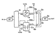
以下に、本発明に係る高周波回路の第1実施形態について図面を参照しつつ説明する。図1は本発明の高周波回路を適用して構成された電力増幅器を模式的に示すブロック図である。
【0037】
同図に示すように、本実施形態に係る電力増幅器は、入力整合回路3iと、この入力整合回路3iからの信号を分岐させる接続手段2iと、高出力増幅器セルブロック1aと、低出力増幅器セルブロック1bと、これら高出力増幅器セルブロック1a及び低出力増幅器セルブロック1bから信号が入力される接続手段2oと、出力整合回路3oとを備えている。
【0038】
高出力増幅器セルブロック1aは、入出力信号について交流的に並列接続された増幅器セルを有しており、これらの増幅器セルに並列に直流電源を供給するものである。一方、低出力増幅器セルブロック1bは、入出力信号について交流的に並列接続された増幅器セルを有しており、これらの増幅器セルに直列に直流電源を供給するものである。
【0039】
上記各増幅器セルブロック1a及び1bは、信号入力端子INa或いはINb、信号出力端子OUTa或いはOUTb、電源電圧端子Vdca或いはVdcb、制御電圧端子Vcnta或いはVcntbを有する。また、接続手段2i,2oは、本実施形態においては、受動素子、例えばコイル、コンデンサで構成されるとともに、図2に示すように、例えば伝送路からなる分岐回路を形成している。
【0040】
(増幅器セルブロックの構成)
上述した高出力増幅器セルブロック1a及び低出力増幅器セルブロック1bの構成について詳述する。図3(a)及び(b)は、高出力増幅器セルブロック1a及び低出力増幅器セルブロック1bの内部構成を示す回路図である。なお、本実施形態における増幅器セル4a,4b,4c,4dは、同じサイズのトランジスタからなる。
【0041】
図3(a)に示すように、本実施形態に係る高出力増幅器セルブロック1aは、2つの増幅器セル4a及び4bを有しており、これら増幅器セル4a,4bは、入出力信号について並列に接続されているとともに、直流電源電圧Vdcaについても並列に接続されている。また、制御電圧Vcntも増幅器セル4a,4bに並列に与えられる。
【0042】
図3(b)に示すように、本実施形態に係る低出力増幅器セルブロック1bは、2つの増幅器セル4c及び4dを有しており、これら増幅器セル4c,4dは、入出力信号について並列接続されているとともに、直流電源電圧Vdcについては直列に接続されている。また、制御電圧Vcntは増幅器セル4c,4dに並列に与えられる。
【0043】
低出力増幅器セルブロック1bにおいて増幅器セル4c及び4dは、例えばバイアスTのような交流直流分割手段5で接続されており、この交流直流分割手段5によって、増幅器セル4cの交流の接地を実現し、直流は増幅器セル4dの直流電源端子に加えられる。この結果、増幅器セル4c,4dに加わる直流電源電圧は分配されて1/2ずつになる。
【0044】
そして、本実施形態においては、高出力増幅器セルブロック1aの増幅器セル4a,4bと、低出力セルブロック1bの増幅器セル4c,4dとの数が同じであるため、入出力インピーダンスは理想的には等しくなる。従って、共通の入出力整合回路3i及び3oを使うことで負荷線の傾きを同じにすることができる。この場合、高出力増幅器セルブロック1aと、低出力増幅器セルブロック1bとでは電源電圧が1/2で、負荷線が同じであるから最大電流も1/2になり、最大出力電力を1/4(−6dB)にすることができる。
【0045】
本実施形態では、図19(b)でバイアス電圧B1がバイアス電圧B2の1/2になった状態と等しい。例えば、最大出力電力30dBmの電力増幅器を構成する場合、高出力電力増幅器の最大出力電力を30dBmに設定すると、低出力電力増幅器の最大出力電力は電源電圧1/2により24dBm程度となる。
【0046】
出力電力が24dBm以上では、高出力増幅器セルブロック1aを動作させて、低出力増幅器1bは非動作状態とする。図14で説明しているように、最大出力電力30dBmより出力電力が低下するのに伴い効率は低下する。
【0047】
出力電力が低出力増幅器セルブロックの最大出力電力である約24dBmでは、効率が35.4%にまで低下しているが、高出力増幅器セルブロック1bを非動作状態として低出力増幅器ブロック1bを動作状態とすることで再び効率が72%に回復し、さらなる出力電力の低下に伴い効率はほぼ35%まで低下していく。増幅器セル簿ロックを複数も受けることにより、さらに低出力時でも再び効率をほぼ72%まで回復させることができるので、図14(a)の特性は約6dB間隔の鋸歯状になる。
【0048】
図4は、図3に示した増幅器セルブロックの等価回路図である。図4(a)は高出力増幅器セルブロック1a、図4(b)は低出力増幅器セルブロック1bを表している。同図において、C1,C2は直流阻止容量、L1,L2はRFチョーク、R1は安定化抵抗、Q1,Q2はバイポーラトランジスタである。なお、Q1,Q2が電界効果トランジスタであっても本発明の効果は得られる。
【0049】
図4(b)中のC3はQ1とQ2のコレクタを直流的に分割するための直流阻止容量である。また、この実施形態では交流直流分割手段5として、C4,L4からなるフィルタを用いている。すなわち、C4によりQ1の信号周波数における交流的な接地を実現している。
【0050】
なお、本実施形態において「交流的に並列接続された増幅器セル」とは、対象となるほぼ同一サイズの増幅器セルに対してほぼ同相、ほぼ等振幅で接続することを意味する。厳密には分布定数回路の立場からは、同相、等振幅での接続は難しいため、例えば、図3におけるセルブロック4aと4b、4cと4d、図4のQ1とQ2にい対して或いは、それぞれの内部のさらに細分化されたセルに対して、入力側での電力の分配及び出力側での電力の合成の効率がそれぞれ50%以上であることを「交流的に並列接続された増幅器セル」と表現する。この分配及び合成の効率とは、N分岐の場合、分配及び合成回路の共通端子Tが、各分岐ポートNへの通過のSパラメータをベクトルSNTとした場合、
(|S1 T+S2 T+S3 T+…Sn T|)/(|S1 T|+|S2 T|+|S3 T|+…|Sn T|)
で与えられる。
【0051】
また、本実施形態において「並列に直流電源を供給する」とは、各セルにほぼ同電位の電圧を与えることを意味する。厳密には回路損失による電圧降下で正確に同電位を与えることは難しいため、例えば、図3におけるセルブロック4a〜4cに対して、或いはそれぞれの内部のさらに細分化されたセルに対して、±20%以内の誤差で電圧を与えることを「並列に直流電源を供給する」という表現を用いる。
【0052】
さらに、本実施形態において、「直列に電流電源を供給する」とは、例えば図4(b)に示すように、「交流的に並列接続された増幅器セル」であるQ1,Q2において、直流電流がQ1のトランジスタセルのコレクタからQ1のエミッタを経てQ2のコレクタに入りQ2で接地される等して、Q1のコレクタに与えられた電圧がこれら複数のトランジスタセルに分割して与えられることを意味する。この例では、バイポーラトランジスタのエミッタ接地の場合について説明したが、電界効果トランジスタや、異なる接地形態においても、複数のトランジスタに分割して電圧を与えることを意味する。
【0053】
(動作及び作用)
そして、上述した構成を有する本実施形態に係る電力増幅器は、以下のように動作する。
【0054】
先ず、入力端子INより入力された信号は、入力整合回路3iと接続手段2iを経て高出力増幅器セルブロック1aおよび低出力セルブロック1bに入力される。高出力増幅器セルブロック1aおよび低出力増幅器セルブロック1bの出力信号は接続手段2oと出力整合回路3oを経て端子OUTから出力される。
【0055】
このとき、本実施形態に係る高周波回路では、出力すべき電力に応じて増幅器セルブロック1a又は1bが選択され、Vcnt電圧により増幅動作状態とハイインピーダンスの非動作状態に切り替えられる。増幅動作状態を取るのは常に1つの増幅器セルブロックのみである。例えば、図2に示しているように、高出力増幅器セルブロック1aが増幅動作状態にあり、低出力増幅器セルブロック1bがハイインピーダンス状態となる。
【0056】
ハイインピーダンス状態にある低出力増幅器セルブロック1bの入力および出力インピーダンスは容量のCi,Coで表すことができる。オープン容量に並列に入る抵抗成分は高出力セルブロック1aの出力インピーダンスに対して十分に大きく損失にはならないためここでは無視した。高出力増幅器セルブロック1aの出力ノード6aから見た負荷インピーダンスは、分岐点ノード6cの先に出力整合回路3oとオープン容量Co付きスタブの並列接続となる。但し、オープン容量Co付きスタブのインピーダンスが短絡条件を満たさないように6a,6c間および6b,6c間のノード間距離を選ぶ必要がある。動作しないトランジスタをハイインピーダンス状態にすることで、スイッチを使わずに増幅器セルブロックを選択できる。
【0057】
[第2実施形態]
次いで、本発明の第2実施形態について説明する。上述した第1実施形態では、図1乃至図4に示したように、増幅器セルブロックが2つの場合について説明したが、本発明は、これに限定されるものではない。例えば、上述した第1実施形態では2段であった低出力増幅器セルブロックの直流電源に対する直列段数を、4段、8段と増すことができる。図5に3つのセルブロックを用いて、12dB以上のダイナミックレンジが得られる例を示す。
【0058】
同図に示すように、本実施形態に係る電力増幅器は、入力整合回路3iと、この入力整合回路3iからの信号を分岐させる接続手段2i’と、高出力増幅器セルブロック1cと、中出力増幅器セルブロック1dと、低出力増幅器セルブロック1eと、これら高出力増幅器セルブロック1c乃至低出力増幅器セルブロック1eから信号が入力される接続手段2o’と、出力整合回路3oとを備えている。
【0059】
詳述すると、図6(a)に示すように、本実施形態に係る高出力増幅器セルブロック1cは、4つの増幅器セル4e〜4hを有しており、これら増幅器セル4e〜4hは、入出力信号について並列に接続されているとともに、直流電源電圧Vdccについても並列に接続されている。また、制御電圧Vcntcも増幅器セル4e〜4hに並列に与えられる。
【0060】
また、図6(b)に示すように、本実施形態に係る中出力増幅器セルブロック1bは、4つの増幅器セル4i及び4lを有しており、これら増幅器セル4i〜4lは、入出力信号について並列接続されている。また、直流電源電圧Vdcdについては増幅器セル4iと4j、及び増幅器セル4kと4lが2つ一組になって直列に接続され、各組の1段目の増幅器セル4iと4kは並列に接続されている。また、制御電圧Vcntdは増幅器セル4i〜4lに並列に与えられる。
【0061】
この中出力増幅器セルブロック1dおける増幅器セル4iと4j、4kと4lは、例えばバイアスTのような交流直流分割手段5で接続されており、この交流直流分割手段5によって、増幅器セル4i,4kについての交流の接地を実現し、直流は各2段目の増幅器セル4j又は4lの直流電源端子に加えられる。この結果、各増幅器セル4i〜4lに加わる直流電源電圧は分配されて1/2ずつになる。
【0062】
さらに、図6(c)に示すように、本実施形態に係る低出力増幅器セルブロック1eは、4つの増幅器セル4m〜4pを有しており、これら増幅器セル4m〜4pは入出力信号について並列接続されているとともに、直流電源電圧Vdceについては直列に接続されている。また、制御電圧Vcnteは増幅器セル4m〜4pに並列に与えられる。
【0063】
この低出力増幅器セルブロック1eにおける増幅器セル4m〜4pは、例えばバイアスTのような交流直流分割手段5を介して直列に接続されており、この交流直流分割手段5によって、増幅器セル4m〜4oについての交流の接地を実現し、直流は各増幅器セル4n〜4pの直流電源端子に加えられる。この結果、増幅器セル4m〜4pに加わる直流電源電圧は分配されて1/4ずつになる。
【0064】
このような本実施形態に係る電力増幅器によれば、3つの増幅器セルブロック1c〜1eを接続することによって上述した第1実施形態の場合に比べてダイナミックレンジを広くとることができる。なお、増幅器セルブロックの直電源に対する直列段数をさらに多段とすることにより、容易にダイナミックレンジを広げることができる。例えば、4つの増幅器セルブロックを用いて各セルブロックを8分割された増幅器セルで構成し、最大で8段(1/8)の直流電流の分割を行えば、18dB以上のダイナミックレンジが与えられる。
【0065】
[第3実施形態]
次いで、本発明の第3の実施形態について説明する。上述した第1実施形態では、図4に示したように、直流電源電圧VdcはL2を介して導入しており、直流阻止容量C2により出力端子へ直流が流れるのを防いでいる。本実施形態では、図7に示すように、第2の接続手段2oとして直流を流せる回路用いることにより、直流電源電圧Vdcをノード6c側から与える。
【0066】
詳述すると、本実施形態に係る高出力用増幅器セルブロック1a’は、第1の接続手段2iから入力される信号を、直流阻止容量C1Hを介して、バイポーラトランジスタQ1H,Q2Hに並列に入力させる構造とするとともに、制御電圧Vcnt1を、安定化抵抗R1H及びRFチョークL1Hを介してバイポーラトランジスタQ1H,Q2Hに並列に入力させる。Vdcは、L2を介して第2の接続手段2o側からバイポーラトランジスタQ1H,Q2Hに並列に入力させる。
【0067】
一方、低出力増幅器セルブロック1b’は、第1の接続手段2iから入力される信号を、直流阻止容量C1Lを介して、バイポーラトランジスタQ1L,Q2Lに並列に入力させる構造とするとともに、制御電圧Vcnt2を、安定化抵抗R1L及びRFチョークL1Lを介してバイポーラトランジスタQ1L,Q2Lに並列に入力させる。
【0068】
この低出力増幅器セルブロック1b’は、Vdcは、L2を介して第2の接続手段2o側からバイポーラトランジスタQ1H,Q2Hに交流的に直列に入力させる。すなわち、直流阻止容量C3及びRFチョークLにより、直流のみがバイポーラトランジスタQ1HからQ2Hに流れるようにする。また、デカップリング容量C3により交流の接地を実現している。
【0069】
そして、図7に示すように、図4(a)に示した高出力セルブロック1a及び図4(b)に示した低出力セルブロック1bからC2とL2を取り除き、第2の接続手段2oのノード6cより、L2を介して共通の電源端子Vdcで直電源を与えている。なお、C2は整合回路3oへの直流カットである。
【0070】
このような第3実施形態によれば、直流電源電圧Vdcは、ノード6c側から供給されるため、上述した第1実施形態におけるL2,C2(図4参照)は不要にすることができ、回路面積の縮小化を図ることができる。
【0071】
なお、この実施形態の変更例としては、L2,C2を図7に示した位置には置かずに、例えば出力整合回路3o内のオープンスタブから直流電源圧を供給するようにすることもできる。
【0072】
[第4実施形態]
次いで、本発明の第4実施形態について説明する。上述した第1実施形態乃至第3実施形態で説明した電力増幅器において、増幅器セルブロックが増えた場合、制御信号Vcntの本数が増える問題が生じるが、以下のような手段により解決することができる。
【0073】
上述した第3実施形態と同様の手法により、Vcnt1、Vcnt2の2つの制御線を共通化して第1の接続手段側から供給することも可能である。図8にその一例を示す。
【0074】
詳述すると、同図に示すように、本実施形態に係る高出力増幅器セルブロック1a”は、第1の接続手段2iから入力される信号を、直流阻止容量C5Hを介して、バイポーラトランジスタQ1H,Q2Hに並列に入力させる構造とするとともに、制御電圧Vcntも第1の接続手段2i側からバイアス回路BCHに入力する。このバイアス回路BCHは制御電圧Vcntに応じて制御信号Vcnt1を発生させるものであり、このバイアス回路BCHで発生されたVcnt1は、バイポーラトランジスタQ1H,Q2Hに並列に入力される。なお、Vdcは、上移した第3実施形態と同様の構成により、第2の接続手段2o側からバイポーラトランジスタQ1H,Q2Hに並列に入力させる。
【0075】
一方、低出力増幅器セルブロック1b”は、第1の接続手段2iから入力される信号を、直流阻止容量C1Lを介して、バイポーラトランジスタQ1L,Q2Lに並列に入力させる構造とするとともに、制御電圧Vcnt2も第1の接続手段2i側からバイアス回路BCLに入力する。このバイアス回路BCLは制御電圧Vcntに応じて制御信号Vcnt2を発生させるものであり、このバイアス回路BCLで発生されたVcnt2は、バイポーラトランジスタQ1L,Q2Lに並列に入力される。
【0076】
この低出力増幅器セルブロック1b”においてVdcは、第2の接続手段2o側からバイポーラトランジスタQ1H,Q2Hに交流的に直列に入力される。すなわち、直流阻止容量C3及びRFチョークLにより、直流のみがバイポーラトランジスタQ1HからQ2Hに流れるようにする。また、デカップリング容量C3により交流の接地を実現している。
【0077】
そして、このような本実施形態に係る電力増幅器では、バイアス回路BCH及びBCLにより、共通化された制御電圧Vcntの電圧に応じてVcnt1及びVcnt2が発生される。BCH及びBCLにて発生された制御電圧Vcnt1及びVcnt2は、高周波チョークインダクタL6H及びL6Lを介してトランジスタQ1H及びQ2H、Q1L、Q2Lに供給される。
【0078】
本実施形態に係る電力増幅器によれば、制御信号Vcntを各増幅器セルブロックについて共通のものとすることによって、増幅器セルブロックの数が増幅した場合であっても、制御信号用の配線量を低減することができ、回路の縮小化を図ることができる。
【0079】
なお、複数本の制御信号Vcntを2進数化或いは多進数化して制御線の本数を削減し、各増幅器セルブロックのバイアス回路にてデコードして制御信号を各々生成することもできる。
【0080】
[第5実施形態]
次いで、本発明の第5実施形態について説明する。図9乃至図11は、第5実施形態に係る電力増幅器を示す説明図である。
【0081】
上述した第1実施形態乃至第4実施形態で説明した電力増幅器において、増幅器セルブロックは、図9(a)に示すように、個別の半導体チップに搭載することができる。すなわち、高出力増幅器セルブロック1a及び低出力増幅器セルブロック1bをそれぞれ独立した半導体チップで形成し、基板GND上に搭載する。この場合、第1及び第2の接続手段2i,2oとは、ボンディングワイヤで接続し、制御電圧Vcnt1及びVcnt2も基板GND外部からボンディングワイヤで導入する。
【0082】
また、同図(b)に示すように、複数の増幅器セルブロックを同一の半導体チップ上に搭載するようにしてもよい。すなわち、高出力増幅器セルブロック1a及び低出力増幅器セルブロック1bを同一の半導体チップで形成し、基板GND上に搭載する。この場合においても、第1及び第2の接続手段2i,2oとは、ボンディングワイヤで接続し、制御電圧Vcnt1及びVcnt2も基板GND外部からボンディングワイヤで導入する。同一のチップに搭載する場合には、接地電極を広くとれるので、接地インダクタンスを低減することができる。
【0083】
さらに、複数の増幅器セルブロックを同一の半導体チップ上に搭載した場合には、同図(c)に示すように、接続手段2i及び2oのT分岐の一部をチップ上に組み込むようにすることもできる。
【0084】
また、異なる増幅器セルブロックの増幅器セル同士をインターリーブに配置することができる。すなわち、図10(a)に示すように、チップ上に高出力増幅器セルブロック1aと、低出力増幅器セルブロック1bとを千鳥状に配置したり、同図(b)に示すように、高出力増幅器セルブロック1aと、低出力増幅器セルブロック1bとを交互に配列してもよい。
【0085】
本発明においては、高出力増幅器セルブロック1aと低出力増幅器セルブロック1bとは、常にいずれか一方のみが動作するため、発熱するセルブロックが分散配置されることとなり、異なる出力の増幅器セルブロック同士であれば近接して配置しても発熱源が密集することがないことから、発熱対策、接地インダクタンス対策のために素子を間引く必要がなく、チップ面積の増加を最小限に留めることができる。
【0086】
なお、上述した同一チップ上への配置は、図10(a)や図11(a)及び(b)に示すように、チップの形状に応じて複数列に配置してもよい。
【0087】
[第6実施形態]
次いで、本発明の第6実施形態について説明する。図12は、本実施形態に係る電力増幅器の説明図である。
【0088】
上述した第1〜第5実施形態においては、各増幅器セルブロックのトランジスタサイズを揃え、インピーダンスを同じにして、さらに入出力の接続手段において対称系を取り扱ってきた。これは、本発明の動作原理が図19(b)に示すように、バイアス電圧により負荷線を平行移動させようとするものだからである。
【0089】
しかし、実際には、負荷線は直線ではなく、またニー電圧の影響により、必ずしもソースとロードのインピーダンスを固定した負荷線の平行移動が最適とは限らない。このような場合に、増幅器セルブロック毎にソース及びロードのインピーダンスを微調整する必要がある。例を幾つか示す。
【0090】
第1が、図12(a)に示すように、入出力の接続手段2i及び2oを、上下(高出力増幅器セルブロック1aと低出力増幅器セルブロック1bとについて)非対称にする方法である。パターンの太さや長さを変えたり、ボンディングワイヤ長や本数、間隔などを変更したり、チップ部品を装荷することで、インピーダンスの微調整を行うことができる。
【0091】
第2は、増幅器セルブロック毎にトランジスタサイズを変更する方法である。例えば、図12(b)に示すように、高出力増幅器セルブロック1aの数を低出力増幅器セルブロック1bの数より多くすることにより、高出力増幅器セルブロックのトランジスタサイズを低出力増幅器セルブロックより大きくし、インピーダンスの調整を実現する。
【0092】
第3が、チップ上におけるセル配置位置により整合回路までの距離を変化させて、インピーダンスを調整するものである。例えば、図12(c)や図11(b)に示すように、高出力増幅器セルブロック1aを第1の接続手段2i側に偏らせて配置し、低出力増幅器セルブロック1bを第2の接続手段2o側に偏らせて配置する。
【0093】
[第7実施形態]
次いで、本発明の第7実施形態について説明する。本発明の電力増幅器は、無線システムの送受信用増幅器に適用できる。
【0094】
即ち、同図(a)に示すように、本実施形態に係る無線システムは、電波信号を送受信するアンテナ101及び102と、これらアンテナ101や102を切り換え接続するアンテナ共用器/切り換え器103と、上述した各実施形態における増幅回路を内蔵した送信用増幅器104及び受信用増幅器105と、これらの送受信用増幅器104及び105に対して変調又は復調された信号を入出力する変調器106及び復調器108と、送受周波数を生成し、またベースバンド信号処理部109との同期処理を行うシンセ部(シンセサイザ)107とを有する無線部100を備えている。
【0095】
また、本実施形態に係る無線システムは、無線部100から入出力される信号を変換処理するベースバンド信号処理部109と、このベースバンド信号処理部109に対して外部からの信号を入出力する入出力部110を有しており、これら無線部100、ベースバンド信号処理部109、及び入出力部110は、電源112から供給される電源電圧により駆動するとともに、制御部111によりその動作が制御される。なお、入出力部110は、外部からの音声や入力操作を受けるインターフェースとしてマイク110a、キー110dを有しており、また外部への出力インターフェースとしてスピーカ110bや表示部110c、バイブ110eを有している。
【0096】
そして、このような無線システムによれば、マイク110aやキー操作110d等の入出力部110により入力された音声や操作信号は、制御部111の制御によりベースバンド信号処理部109で信号処理され、変調器106を介して送信用増幅器104に入力される。この送信用増幅器104では、上述した各実施形態に係る増幅処理によって増幅され、アンテナ共用器/切り替え器103を介して、アンテナ101や102より送信される。
【0097】
なお、アンテナ101や102で受信された電波は、制御部111の制御によりアンテナ共用器/切り替え器103を介して受信用増幅器105により増幅され、復調器108、ベースバンド信号処理部109により制御信号に変換され、入出力部110のスピーカ110bや表示部110c、バイブ110eの動作を制御する。この場合の受信用増幅器105においても上述した各実施形態に係る電力増幅器を採用してもよい。
【0098】
また、本発明は図13(b)に示すような、移動体通信システムの基地局についても採用することができる。
【0099】
即ち、同図(b)に示すように、本実施形態に係る移動体通信システムは、電波信号を送受信するアンテナ201及び202と、これらアンテナ201や202を切り換え接続するアンテナ共用器/切り換え器203と、上述した各実施形態における増幅回路を内蔵した送信用増幅器204及び受信用増幅器205と、これらの送受信用増幅器204及び205に対して変調又は復調された信号を入出力する変復調器206とを有する無線部200を1以上備えている。
【0100】
また、本実施形態に係る移動体通信システムは、無線部200から入出力される信号を処理するベースバンド信号処理部207と、このベースバンド信号処理部207に対して外部からの信号を入出力する伝送路接続部208を有しており、これら無線部200、ベースバンド信号処理部207、及び伝送路接続部208は、電源210から供給される電源電圧により駆動するとともに、制御部209によりその動作が制御される。
【0101】
そして、このような移動体通信システムでは、外部から入力された信号は、伝送路接続部208を通じてベースバンド信号処理部207に入力され、このベースバンド信号処理部207において信号処理され、変調器206を介して送信用増幅器204に入力される。この送信用増幅器204では、上述した各実施形態に係る増幅処理によって増幅され、アンテナ共用器/切り替え器203を介して、アンテナ201や202より送信される。
【0102】
なお、アンテナ201や202で受信された電波は、アンテナ共用器/切り替え器203を介して受信用増幅器205により増幅され、変復調器206、ベースバンド信号処理部207により制御信号に変換され、伝送路接続部208を通じて外部に出力される。
【0103】
このように本発明の電力増幅器は、特に出力電力範囲の広い電力増幅器を必要とするシステムに好適である。例えば、上述したような移動局との通信や、或いは固定局同士であっても電波伝播の環境が変化しやすい場合に有効である。また、携帯電話などの移動体通信システム、とりわけ広いダイナミックレンジを必要とするCDMA方式によるシステムでは有効である。
【0104】
【発明の効果】
本発明によれば、本発明によれば、広い出力電力範囲にわたって高効率動作が可能な電力増幅器を、スイッチ、可変整合回路、DC−DCコンバータ等の可変電圧源を用いずに実現することができる。本発明に必要な回路はMMICに搭載可能であるため、消費電力にシビアな携帯電話用の電力増幅器などに応用することができる。この結果、電話機の連続通話時間を2倍以上に延長する効果が期待できる。
【図面の簡単な説明】
【図1】本発明の第1実施形態に係る電力増幅器の結線を説明するブロック図である。
【図2】本発明の第1実施形態の動作状態を説明するブロック図である。
【図3】本発明の第1実施形態に係る高出力増幅器セルブロック及び低出力増幅器セルブロックを示すブロック図である。
【図4】本発明の第1実施形態に係る増幅器セルブロックの等価回路図である。
【図5】本発明の第2実施形態に係る電力増幅器のブロック図である。
【図6】本発明の第2実施形態に係る高出力増幅器セルブロック、中出力増幅器セルブロック、及び低出力増幅器セルブロックを示すブロック図である。
【図7】本発明の第3実施形態に係る電力増幅器の等価回路図である。
【図8】本発明の第4実施形態に係る電力増幅器の等価回路図である。
【図9】本発明の第5実施形態に係る電力増幅器のレイアウト図である。
【図10】本発明の第5実施形態に係る電力増幅器のレイアウト図である。
【図11】本発明の第5実施形態に係る電力増幅器のレイアウト図である。
【図12】本発明の第6実施形態に係る電力増幅器のレイアウト図である。
【図13】本発明の第7実施形態に係る通信システムのブロック図である。
【図14】電力増幅器のRF出力電力と効率の関係を説明するグラフである。
【図15】電力増幅器の低出力時における効率の低下を説明する原理図である。
【図16】従来の増幅回路の説明図である。
【図17】従来の増幅回路の説明図である。
【図18】従来の増幅回路の説明図である。
【図19】従来の増幅回路の説明図である。
【符号の説明】
1a〜1e 増幅器セルブロック
2i,2i’,2i” 第1の接続手段
2o,2o’,2o” 第2の接続手段
3i 入力整合回路
3o 出力整合回路
4a〜4l 増幅器セル
5 交流直流分離手段
6a,6b,6c 第2の接続手段の中のノード
101,102,201,202 アンテナ
100,200 通信部
104,204 送信用増幅器
105,205 受信用増幅器
110 入出力部
111,209 制御部
207 ベースバンド信号処理部
208 伝送路接続部[0001]
TECHNICAL FIELD OF THE INVENTION
The present invention relates to a high-frequency circuit of a high-efficiency power amplifier having a wide output power range and a communication system including the high-frequency circuit provided in, for example, a mobile phone.
[0002]
[Prior art]
In general, in a power amplifier, the power added efficiency increases with the output power and reaches a maximum value near the saturation of the output power, so that the efficiency decreases at low output. FIG. 14A is an example of the relationship between efficiency and output power at the time of low output of a general amplifier. Here, the efficiency is obtained by dividing the RF (high output) output power by the DC (direct current) input power, and refers to the collector efficiency of the bipolar transistor and the drain efficiency of the field effect transistor. FIG. 14B shows the reciprocal of the efficiency shown in FIG. 14A on a logarithmic scale.
[0003]
As shown in the figure, the efficiency was 72% when the output power was 30 dBm (dBmW, hereinafter abbreviated as dBm), but was 21.8% at 20 dBm output, 4.7% at 10 dBm output, and 1.5 at 5 dBm output. %. The applied DC power increases to 1.4 times the RF output power at 30 dBm output, 4.6 times at 20 dBm output, 21 and 21 times at 10 dBm output, and 67.1 times at 5 dBm.
[0004]
The reason why the efficiency is degraded at the time of low output will be described using a simple idealized transistor model. FIG. 15 is a graph showing the relationship between current and voltage in alternating current.
[0005]
As shown in the figure, the load line is represented by a chain line KB, the output voltage is represented by a sine wave with a bias voltage averaged, and the output current is represented by a half-wave rectified wave Iout (t). Assume. In this case, point B in the figure corresponds to a bias point.
[0006]
In the case of FIG. 15, the operation is a class B operation. The RF output power is obtained by calculating the effective value of the fundamental wave component Vout of the output power and the fundamental wave component I of the output current.1It is given by the product of (t) and the effective value. One-half of the area of the rectangle having the points R and B as diagonals corresponds to the RF output power.
[0007]
Since the DC input power is given by the product of the bias and the average value of the output current Iout (t), it corresponds to the area of a quadrilateral having the points D and B as diagonals (hereinafter, referred to as a quadrilateral DB). . The efficiency is given by the area ratio of the two.
[0008]
15B, the current amplitude and the voltage amplitude are halved in FIG. 15B, and the RF output power is 1 /. On the other hand, since the DC current is the average value of the RF current, it is halved at the same rate, but since the DC voltage is fixed at the point B, the area of the square DB is 2. As a result, each time the RF output power becomes 1/4 (-6 dB), the efficiency is reduced by half. Actually, the rate of deterioration of efficiency is more than halved due to the AB class operation or the effect of the knee voltage.
[0009]
Conventionally, there is an amplifier circuit shown in FIG. 16 as a means for compensating for such deterioration in efficiency at the time of low output.
[0010]
That is, in the conventional high-frequency circuit, a plurality of amplifiers having different maximum output powers, AMP1 (maximum output −20 dBm), AMP2 (
[0011]
However, as can be seen from the gain diagram shown in FIG. 16B, in the above-described conventional amplifier circuit, when the output power is in the range of 5 dBm or more and 30 dBm or less (B in the figure), the maximum output power of AMP3 is 30 dBm. In addition, although the maximum output power of the AMP2 is 5 dBm, a power that is smaller by 25 dB at the maximum may be output, so that the efficiency is deteriorated. Similarly, in the output power range of −20 dBm or more and 5 dBm or less (D in the figure), power consumption increases due to deterioration in efficiency, though not as much as B described above.
[0012]
Further, as shown in FIG. 3A, since the gain of each stage is usually about 25 dB, it is difficult to significantly reduce the deterioration of the efficiency by the above method. On the other hand, a method in which the number of amplification stages is further reduced may be considered. In this case, a step of 10 dB to 15 dB corresponding to a gain per transistor stage is considered to be a practical minimum unit.
[0013]
In this case, it is necessary to make the input and output impedances remarkably uniform, so that the conjugate matching of the preceding and succeeding transistors would normally have to be achieved, but once converting to high impedance, the loss increases and the circuit configuration becomes complicated. May be invited.
[0014]
Therefore, conventionally, a method of optimizing a load line of an amplifier in an arbitrary stage according to output power has been proposed. FIG. 17 is a circuit diagram schematically showing a circuit for realizing the conventional optimization method.
[0015]
The circuit shown in FIG. 17 (a) is a method for switching the effective transistor size of the amplifier, in which a plurality of
[0016]
According to such a conventional amplifier circuit, by appropriately switching and combining the plurality of
[0017]
[Problems to be solved by the invention]
In the case of the circuit shown in FIG. 17A, the maximum output power is halved by halving the size of the transistor, and the efficiency can be maximized at a small power of about 3 dB. However, to control the range of 24 dB according to FIG. 16, 24 dB ÷ 3 dB = 8, which is 28Is required for the transistor cell divided into 256.
[0018]
In the circuit shown in FIG. 17A, the matching condition must be satisfied even if the slope of the load line changes from BK1 to BK2. Therefore, the matching circuit must be changed at the same time. As such a variable matching circuit, a combination of a
[0019]
Further, as means for compensating for the deterioration of the efficiency at the time of low output, there is an amplifier circuit shown in FIG. This amplifier circuit is a method of optimizing a power supply voltage supplied to an amplifier according to output power. As shown in FIG. 19B, a voltage Vdc applied to a
[0020]
In the circuit shown in FIG. 19A, the output power can be adjusted steplessly. However, as shown in FIG. 19B, since the slope of the load lines (K1B1 and K2B2) does not change, the variable matching circuit can be adjusted. Is basically unnecessary, and when the power supply voltage is simply halved, the RF output power at which the efficiency becomes maximum is reduced by about 6 dB.
[0021]
However, as a high-efficiency variable voltage source capable of supplying a large current consumed by the power amplifier, a resistor L and a capacitor C as shown in FIG. 19C are appropriately changed by switches Q1 and Q2 controlled by a control circuit. There is a step-down DC-DC converter to be connected. However, the minimum output voltage is about 1 V in relation to the reference voltage of the internal regulator, and the efficiency of the variable voltage source deteriorates at the time of low voltage output. However, it is difficult to maintain high efficiency in a wide output power range, and the mounting area is large.
[0022]
For example, in CDMA communication, the transmission output power must be changed according to the distance between the mobile station and the base station. This is because radio waves from a plurality of mobile stations need to be aligned at the base station receiver input end. Similarly, it is desirable that radio waves coming from a plurality of base stations be aligned at the receiver end of the mobile station.
[0023]
Therefore, in a CDMA communication system, transmission power control is performed, and the transmission power changes in a range (dynamic range) of about 75 dB. For this reason, it is required that the power added efficiency of the power amplifier be high other than at the time of the maximum output power. The probability density function of the transmission power generally has a normal distribution, and the average transmission power of the mobile terminal varies from 10 dBm to 16 dBm depending on system factors such as the arrangement of base stations. Therefore, it is necessary to always keep the power added efficiency high within a range of about 0 dBm (at low output) to 30 dBm (at high output).
[0024]
Therefore, the present invention has been made to solve the above-described problems, and realizes a power amplifier having a wide dynamic range in which power addition efficiency is unlikely to be degraded even at low output with a simple circuit having a small mounting area. It is another object of the present invention to provide a high-frequency circuit capable of reducing the size and weight of a communication system by employing such a circuit and a communication system including the high-frequency circuit.
[0025]
[Means for Solving the Problems]
In order to solve the above-mentioned problem, the invention according to
[0026]
The invention according to
[0027]
The invention according to
[0028]
The invention according to claim 4 is a high-output amplifier cell block that supplies DC power in parallel to a first amplifier cell connected in parallel with respect to input / output signals, and an AC parallel connection in which the input / output signals are connected with AC. A low-power amplifier cell block for supplying DC power to the second amplifier cell in series, first connection means for connecting the input side of the high-power amplifier cell block and the input side of the low-power amplifier cell block, A high-frequency circuit having an amplifier cell block and second connection means for connecting the output side of the low-output amplifier cell block; and amplifying operation of only one of the high-output amplifier cell block and the low-output cell block. And a control unit for controlling another amplifier cell block to a high impedance state, and an antenna for receiving a signal output from the high frequency circuit. Is a communication system characterized in that it comprises and.
[0029]
The invention according to
[0030]
According to the present invention, the high-output amplifier cell block is driven at the time of high output, and the low-output amplifier cell block is driven at the time of low output. It is possible to reduce wasteful power consumption due to driving of the high-output amplifier cell block. Further, in the high-output amplifier cell block, since the amplifier cells are connected in parallel in an AC manner, a voltage having substantially the same phase as each of the amplifier cells and substantially the same voltage as the input voltage is applied. High-power amplification can be realized without generating a phase shift. On the other hand, in the low-output amplifier cell block, since the amplifier cell blocks are connected in series in an alternating current manner, a distributed low voltage is applied to each amplifier cell with substantially the same phase, so that a voltage between the amplifier cells is reduced. Low output amplification can be realized without causing a phase shift.
[0031]
Furthermore, according to the present invention, according to the output power, only one of the amplifier cell blocks takes the amplification operation state, and the other amplifier cell blocks enter the high impedance state. The means can be regarded as a high-impedance open capacitance, and does not affect the cell block in the operating state.
[0032]
In particular, by increasing the number of series stages with respect to the power supply voltage of the amplifier cell, it is possible to reduce the output power at which the maximum efficiency is obtained by about 6 dB per stage. Since a variable power supply such as a switch for switching a signal path, a variable matching circuit, and a DC-DC converter is not required, the size is reduced.
[0033]
In the present invention, the term "amplifier cells connected in parallel in alternating current" means that the target amplifier cells of substantially the same size are connected with substantially the same phase and substantially equal amplitude. Strictly speaking, from the standpoint of a distributed constant circuit, connection at the same phase and equal amplitude is difficult. For example, the efficiency of power distribution on the input side of multiple cell blocks and power combining on the output side are 50%, respectively. The above is expressed as "amplifier cells connected in parallel in alternating current". In the case of N branches, the common terminal T of the distribution and combination circuit converts the S parameter of passage to each branch port N into a vector SNTThen,
(| S1 T+ S2 T+ S3 T+ ... Sn T|) / (| S1 T| + | S2 T| + | S3 T| + ... | Sn T|)
Given by
[0034]
In the present invention, “supplying a DC power supply in parallel” means applying a voltage having substantially the same potential to each cell. Strictly speaking, it is difficult to give exactly the same potential due to a voltage drop due to circuit loss. For example, for a plurality of cell blocks or for a further subdivided cell in each of them, within ± 20% Giving a voltage with an error is referred to as "supplying DC power in parallel".
[0035]
Furthermore, in the present invention, "supplying a current power supply in series" means, for example, in the amplifier cells Q1 and Q2 which are connected in parallel with each other in an alternating current state, the DC current of the transistor cell is Q1 from the emitter of the transistor cell Q1. Means that the voltage applied to the collector of Q1 is divided and applied to the plurality of transistor cells by entering the collector of Q2 via Q2 and grounding at Q2. In this example, the case where the emitter of the bipolar transistor is grounded has been described, but it means that a voltage is divided and applied to a plurality of transistors even in a field effect transistor or a different grounding form.
[0036]
BEST MODE FOR CARRYING OUT THE INVENTION
[First Embodiment]
(overall structure)
Hereinafter, a first embodiment of a high-frequency circuit according to the present invention will be described with reference to the drawings. FIG. 1 is a block diagram schematically showing a power amplifier configured by applying the high-frequency circuit of the present invention.
[0037]
As shown in the figure, the power amplifier according to the present embodiment includes an
[0038]
The high-output
[0039]
Each of the
[0040]
(Configuration of amplifier cell block)
The configuration of the high-output
[0041]
As shown in FIG. 3A, the high-output
[0042]
As shown in FIG. 3B, the low-output
[0043]
In the low-power
[0044]
In this embodiment, since the number of the
[0045]
In the present embodiment, the state is the same as the state in which the bias voltage B1 is 1 / of the bias voltage B2 in FIG. For example, when configuring a power amplifier having a maximum output power of 30 dBm, if the maximum output power of the high output power amplifier is set to 30 dBm, the maximum output power of the low output power amplifier will be about 24 dBm due to the
[0046]
When the output power is 24 dBm or more, the high-output
[0047]
When the output power is about 24 dBm, which is the maximum output power of the low-output amplifier cell block, the efficiency is reduced to 35.4%, but the high-output
[0048]
FIG. 4 is an equivalent circuit diagram of the amplifier cell block shown in FIG. FIG. 4A shows a high power
[0049]
C3 in FIG. 4B is a DC blocking capacitance for dividing the collectors of Q1 and Q2 in a DC manner. In this embodiment, a filter composed of C4 and L4 is used as the AC / DC dividing means 5. That is, AC grounding at the signal frequency of Q1 is realized by C4.
[0050]
In the present embodiment, “amplifier cells connected in parallel in alternating current” means that the target amplifier cells of substantially the same size are connected with substantially the same phase and substantially equal amplitude. Strictly, from the standpoint of a distributed constant circuit, it is difficult to make connections at the same phase and equal amplitude. For example, for the
(| S1 T+ S2 T+ S3 T+ ... Sn T|) / (| S1 T| + | S2 T| + | S3 T| + ... | Sn T|)
Given by
[0051]
In the present embodiment, “supplying DC power in parallel” means applying a voltage having substantially the same potential to each cell. Strictly speaking, since it is difficult to give the same potential accurately by a voltage drop due to circuit loss, for example, for the
[0052]
Further, in the present embodiment, “supplying a current power supply in series” means, for example, as shown in FIG. 4B, that a direct current is supplied to Q1 and Q2 which are “amplifier cells connected in parallel in AC”. Means that the voltage applied to the collector of Q1 is divided and applied to the plurality of transistor cells, for example, from the collector of the transistor cell of Q1 to the collector of Q2 via the emitter of Q1, and grounded at Q2. I do. In this example, the case where the emitter of the bipolar transistor is grounded has been described, but it means that a voltage is divided and applied to a plurality of transistors even in a field effect transistor or a different grounding form.
[0053]
(Operation and action)
The power amplifier according to the present embodiment having the above-described configuration operates as follows.
[0054]
First, a signal input from the input terminal IN is input to the high-output
[0055]
At this time, in the high-frequency circuit according to the present embodiment, the
[0056]
The input and output impedances of the low output
[0057]
[Second embodiment]
Next, a second embodiment of the present invention will be described. In the above-described first embodiment, the case where there are two amplifier cell blocks has been described as shown in FIGS. 1 to 4, but the present invention is not limited to this. For example, the number of series stages for the DC power supply of the low-output amplifier cell block, which is two in the first embodiment, can be increased to four or eight. FIG. 5 shows an example in which a dynamic range of 12 dB or more can be obtained using three cell blocks.
[0058]
As shown in the figure, the power amplifier according to the present embodiment includes an
[0059]
More specifically, as shown in FIG. 6A, the high power
[0060]
As shown in FIG. 6B, the medium output
[0061]
The
[0062]
Further, as shown in FIG. 6C, the low-output
[0063]
The
[0064]
According to such a power amplifier according to the present embodiment, by connecting the three
[0065]
[Third embodiment]
Next, a third embodiment of the present invention will be described. In the above-described first embodiment, as shown in FIG. 4, the DC power supply voltage Vdc is introduced via L2, and the DC blocking capacitance C2 prevents DC from flowing to the output terminal. In this embodiment, as shown in FIG. 7, a DC power supply voltage Vdc is applied from the
[0066]
More specifically, the high-output
[0067]
On the other hand, the low-output
[0068]
In this low-output
[0069]
Then, as shown in FIG. 7, C2 and L2 are removed from the high
[0070]
According to such a third embodiment, since the DC power supply voltage Vdc is supplied from the
[0071]
As a modification of this embodiment, it is also possible to supply the DC power supply voltage from, for example, an open stub in the output matching circuit 3o without placing L2 and C2 at the positions shown in FIG.
[0072]
[Fourth embodiment]
Next, a fourth embodiment of the present invention will be described. In the power amplifiers described in the above-described first to third embodiments, when the number of amplifier cell blocks increases, there is a problem that the number of control signals Vcnt increases, but this can be solved by the following means.
[0073]
In the same manner as in the third embodiment described above, two control lines of Vcnt1 and Vcnt2 can be shared and supplied from the first connection unit side. FIG. 8 shows an example.
[0074]
More specifically, as shown in the figure, the high-output
[0075]
On the other hand, the low-output
[0076]
In this low-output
[0077]
In the power amplifier according to this embodiment, Vcnt1 and Vcnt2 are generated by the bias circuits BCH and BCL according to the voltage of the common control voltage Vcnt. Control voltages Vcnt1 and Vcnt2 generated by BCH and BCL are supplied to transistors Q1H and Q2H, Q1L and Q2L via high-frequency choke inductors L6H and L6L.
[0078]
According to the power amplifier according to the present embodiment, the control signal Vcnt is made common to each amplifier cell block, thereby reducing the amount of control signal wiring even when the number of amplifier cell blocks is amplified. And the circuit can be reduced in size.
[0079]
The control signal Vcnt may be converted into a binary number or a binary number to reduce the number of control lines, and each of the control signals may be generated by decoding with a bias circuit of each amplifier cell block.
[0080]
[Fifth Embodiment]
Next, a fifth embodiment of the present invention will be described. 9 to 11 are explanatory diagrams illustrating a power amplifier according to the fifth embodiment.
[0081]
In the power amplifiers described in the first to fourth embodiments, the amplifier cell block can be mounted on an individual semiconductor chip as shown in FIG. That is, the high-output
[0082]
Further, as shown in FIG. 1B, a plurality of amplifier cell blocks may be mounted on the same semiconductor chip. That is, the high-output
[0083]
Further, when a plurality of amplifier cell blocks are mounted on the same semiconductor chip, a part of the T-branch of the connection means 2i and 2o should be incorporated on the chip as shown in FIG. You can also.
[0084]
Further, amplifier cells of different amplifier cell blocks can be arranged in an interleaved manner. That is, as shown in FIG. 10A, a high-output
[0085]
In the present invention, since only one of the high-output
[0086]
Note that the above-described arrangement on the same chip may be arranged in a plurality of rows according to the shape of the chip, as shown in FIGS. 10 (a), 11 (a) and 11 (b).
[0087]
[Sixth embodiment]
Next, a sixth embodiment of the present invention will be described. FIG. 12 is an explanatory diagram of the power amplifier according to the present embodiment.
[0088]
In the above-described first to fifth embodiments, the symmetric system has been handled in the input / output connection means, with the transistor sizes of the amplifier cell blocks being equalized, the impedance being the same, and the input / output connection means. This is because the operation principle of the present invention is to move the load line in parallel by the bias voltage as shown in FIG.
[0089]
However, in practice, the load line is not a straight line, and due to the effect of the knee voltage, the parallel movement of the load line with the fixed impedance between the source and the load is not always optimal. In such a case, it is necessary to finely adjust the source and load impedance for each amplifier cell block. Here are some examples.
[0090]
First, as shown in FIG. 12A, there is a method in which the input / output connection means 2i and 2o are asymmetrical with respect to the upper and lower sides (with respect to the high-output
[0091]
A second method is to change the transistor size for each amplifier cell block. For example, as shown in FIG. 12B, by making the number of high-output
[0092]
Third, the impedance is adjusted by changing the distance to the matching circuit depending on the cell arrangement position on the chip. For example, as shown in FIG. 12 (c) and FIG. 11 (b), the high-output
[0093]
[Seventh embodiment]
Next, a seventh embodiment of the present invention will be described. The power amplifier of the present invention can be applied to a transmission / reception amplifier of a wireless system.
[0094]
That is, as shown in FIG. 1A, the wireless system according to the present embodiment includes
[0095]
Further, the wireless system according to the present embodiment converts a signal input / output from the
[0096]
According to such a wireless system, voice and operation signals input from the input / output unit 110 such as the
[0097]
The radio waves received by the
[0098]
The present invention can also be applied to a base station of a mobile communication system as shown in FIG.
[0099]
That is, as shown in FIG. 3B, the mobile communication system according to the present embodiment includes
[0100]
Further, the mobile communication system according to the present embodiment includes a baseband
[0101]
In such a mobile communication system, a signal input from the outside is input to a baseband
[0102]
The radio waves received by the
[0103]
Thus, the power amplifier of the present invention is particularly suitable for a system requiring a power amplifier having a wide output power range. For example, this is effective when communication with a mobile station as described above or between fixed stations is performed when the environment of radio wave propagation is likely to change. In addition, the present invention is effective in a mobile communication system such as a mobile phone, especially in a CDMA system requiring a wide dynamic range.
[0104]
【The invention's effect】
According to the present invention, according to the present invention, a power amplifier capable of high-efficiency operation over a wide output power range can be realized without using a variable voltage source such as a switch, a variable matching circuit, and a DC-DC converter. it can. Since a circuit required for the present invention can be mounted on an MMIC, it can be applied to a power amplifier for a mobile phone which is severe in power consumption. As a result, the effect of extending the continuous talk time of the telephone to twice or more can be expected.
[Brief description of the drawings]
FIG. 1 is a block diagram illustrating connection of a power amplifier according to a first embodiment of the present invention.
FIG. 2 is a block diagram illustrating an operation state of the first embodiment of the present invention.
FIG. 3 is a block diagram showing a high power amplifier cell block and a low power amplifier cell block according to the first embodiment of the present invention.
FIG. 4 is an equivalent circuit diagram of the amplifier cell block according to the first embodiment of the present invention.
FIG. 5 is a block diagram of a power amplifier according to a second embodiment of the present invention.
FIG. 6 is a block diagram showing a high power amplifier cell block, a medium power amplifier cell block, and a low power amplifier cell block according to a second embodiment of the present invention.
FIG. 7 is an equivalent circuit diagram of a power amplifier according to a third embodiment of the present invention.
FIG. 8 is an equivalent circuit diagram of a power amplifier according to a fourth embodiment of the present invention.
FIG. 9 is a layout diagram of a power amplifier according to a fifth embodiment of the present invention.
FIG. 10 is a layout diagram of a power amplifier according to a fifth embodiment of the present invention.
FIG. 11 is a layout diagram of a power amplifier according to a fifth embodiment of the present invention.
FIG. 12 is a layout diagram of a power amplifier according to a sixth embodiment of the present invention.
FIG. 13 is a block diagram of a communication system according to a seventh embodiment of the present invention.
FIG. 14 is a graph illustrating the relationship between RF output power and efficiency of a power amplifier.
FIG. 15 is a principle diagram illustrating a decrease in efficiency at the time of low output of the power amplifier.
FIG. 16 is an explanatory diagram of a conventional amplifier circuit.
FIG. 17 is an explanatory diagram of a conventional amplifier circuit.
FIG. 18 is an explanatory diagram of a conventional amplifier circuit.
FIG. 19 is an explanatory diagram of a conventional amplifier circuit.
[Explanation of symbols]
1a-1e Amplifier cell block
2i, 2i ', 2i "First connection means
2o, 2o ', 2o "Second connection means
3i input matching circuit
3o Output matching circuit
4a to 4l amplifier cell
5 AC / DC separation means
6a, 6b, 6c Nodes in second connection means
101, 102, 201, 202 antenna
100,200 communication unit
104,204 Transmission amplifier
105,205 Receiver amplifier
110 Input / output unit
111,209 control unit
207 Baseband signal processing unit
208 Transmission line connection
Claims (5)
前記入出力信号について交流的に並列接続された第2の増幅器セルに直列に前記直流電源を供給する低出力増幅器セルブロックと、
前記高出力増幅器セルブロック及び前記低出力増幅器セルブロックの入力側を接続する第1の接続手段と、
前記高出力増幅器セルブロック及び前記低出力増幅器セルブロックの出力側を接続する第2の接続手段と
を備えることを特徴とする高周波回路。A high-power amplifier cell block for supplying a DC power supply in parallel to a first amplifier cell connected in parallel with respect to input / output signals;
A low-power amplifier cell block for supplying the DC power in series to a second amplifier cell connected in parallel with respect to the input / output signal;
First connection means for connecting the input sides of the high power amplifier cell block and the low power amplifier cell block;
A high-frequency circuit comprising: a second connection unit that connects the output sides of the high-output amplifier cell block and the low-output amplifier cell block.
前記入出力信号について交流的に並列接続された第2の増幅器セルに直列に直流電源を供給する低出力増幅器セルブロックと、
前記高出力増幅器セルブロック及び前記低出力増幅器セルブロックの入力側を接続する第1の接続手段と、
前記高出力増幅器セルブロック及び前記低出力増幅器セルブロックの出力側を接続する第2の接続手段とを有する高周波回路と、
前記高出力増幅器セルブロックと前記低出力セルブロックのうち何れか一つのみを増幅動作状態とし、他の増幅器セルブロックをハイインピーダンス状態とに制御する制御部と、
前記高周波回路から出力された信号を受け取るアンテナとを備えることを特徴とする通信システム。A high-power amplifier cell block for supplying a DC power supply in parallel to a first amplifier cell connected in parallel with respect to input / output signals;
A low-power amplifier cell block for supplying DC power in series to a second amplifier cell connected in parallel with respect to the input / output signal;
First connection means for connecting the input sides of the high power amplifier cell block and the low power amplifier cell block;
A high-frequency circuit having second connection means for connecting the output sides of the high-output amplifier cell block and the low-output amplifier cell block;
A control unit that controls only one of the high-output amplifier cell block and the low-output cell block in an amplification operation state, and controls another amplifier cell block to a high impedance state.
An antenna for receiving a signal output from the high-frequency circuit.
Priority Applications (6)
| Application Number | Priority Date | Filing Date | Title |
|---|---|---|---|
| JP2000103784A JP3600115B2 (en) | 2000-04-05 | 2000-04-05 | High frequency circuit and communication system |
| KR1020010015138A KR100602140B1 (en) | 2000-04-05 | 2001-03-23 | High frequency circuit and communication system |
| DE60124448T DE60124448T2 (en) | 2000-04-05 | 2001-04-05 | High-frequency circuit with high-output amplifier cell unit and low-output amplifier cell unit |
| US09/826,361 US6804500B2 (en) | 2000-04-05 | 2001-04-05 | High frequency circuit using high output amplifier cell block and low output amplifier cell block |
| EP01303251A EP1148633B1 (en) | 2000-04-05 | 2001-04-05 | High frequency circuit using high output amplifier cell block and low output amplifier cell block |
| US10/927,165 US6927625B2 (en) | 2000-04-05 | 2004-08-27 | High frequency circuit using high output amplifier cell block and low output amplifier cell block |
Applications Claiming Priority (1)
| Application Number | Priority Date | Filing Date | Title |
|---|---|---|---|
| JP2000103784A JP3600115B2 (en) | 2000-04-05 | 2000-04-05 | High frequency circuit and communication system |
Publications (2)
| Publication Number | Publication Date |
|---|---|
| JP2001292033A JP2001292033A (en) | 2001-10-19 |
| JP3600115B2 true JP3600115B2 (en) | 2004-12-08 |
Family
ID=18617429
Family Applications (1)
| Application Number | Title | Priority Date | Filing Date |
|---|---|---|---|
| JP2000103784A Expired - Fee Related JP3600115B2 (en) | 2000-04-05 | 2000-04-05 | High frequency circuit and communication system |
Country Status (5)
| Country | Link |
|---|---|
| US (2) | US6804500B2 (en) |
| EP (1) | EP1148633B1 (en) |
| JP (1) | JP3600115B2 (en) |
| KR (1) | KR100602140B1 (en) |
| DE (1) | DE60124448T2 (en) |
Families Citing this family (50)
| Publication number | Priority date | Publication date | Assignee | Title |
|---|---|---|---|---|
| US6377784B2 (en) * | 1999-02-09 | 2002-04-23 | Tropian, Inc. | High-efficiency modulation RF amplifier |
| US6917973B2 (en) * | 2001-01-04 | 2005-07-12 | Intel Corporation | Managing access to a network |
| GB2376384B (en) * | 2001-06-08 | 2005-03-16 | Sony Uk Ltd | Antenna switch |
| FI20011866A0 (en) | 2001-09-21 | 2001-09-21 | Nokia Corp | Multi-input amplifier |
| US6791407B2 (en) * | 2002-01-15 | 2004-09-14 | Mia-Com Eurotec B.V. | Switchable power amplifier |
| US7088969B2 (en) * | 2002-02-12 | 2006-08-08 | Broadcom Corporation | Highly linear power amplifier and radio applications thereof |
| US7113033B2 (en) | 2002-01-31 | 2006-09-26 | Qualcomm Incorporated | Variable impedance load for a variable gain radio frequency amplifier |
| US6957055B2 (en) * | 2002-02-20 | 2005-10-18 | Doron Gamliel | Double balanced FET mixer with high IP3 and IF response down to DC levels |
| US20070060074A1 (en) * | 2002-03-07 | 2007-03-15 | Matsushita Electric Industrial Co., Ltd. | High-efficiency modulating RF amplifier |
| GB2389275B (en) * | 2002-05-31 | 2006-10-25 | Hitachi Ltd | Apparatus for mobile communication system |
| KR100487347B1 (en) * | 2002-11-27 | 2005-05-03 | 엘지전자 주식회사 | High Efficiency Power amplifier |
| US7444124B1 (en) | 2003-05-14 | 2008-10-28 | Marvell International Ltd. | Adjustable segmented power amplifier |
| GB2406748A (en) * | 2003-09-30 | 2005-04-06 | Nokia Corp | Digital broadcast receiver module comprising a loop antenna amplifier and demodulator and means for connecting the module to a mobile terminal |
| DE102004001236B4 (en) * | 2004-01-07 | 2010-08-19 | Infineon Technologies Ag | Power amplifier arrangement with antenna and its use and method for amplifying and emitting a signal |
| JP4137815B2 (en) * | 2004-02-19 | 2008-08-20 | ソニー・エリクソン・モバイルコミュニケーションズ株式会社 | Power amplification device and portable communication terminal device |
| JP3961498B2 (en) * | 2004-02-27 | 2007-08-22 | 松下電器産業株式会社 | High frequency circuit equipment |
| DE102004026168A1 (en) * | 2004-05-28 | 2005-12-22 | Siemens Ag | Adjustment method for obtaining desired radiation performance for antenna of radio communication equipment involves selecting performance booster with highest efficiency for particular performance class from several performance boosters |
| WO2006006244A1 (en) * | 2004-07-14 | 2006-01-19 | Mitsubishi Denki Kabushiki Kaisha | High output amplifier |
| JP2006093773A (en) * | 2004-09-21 | 2006-04-06 | Renesas Technology Corp | High frequency power amplification module |
| US7769355B2 (en) * | 2005-01-19 | 2010-08-03 | Micro Mobio Corporation | System-in-package wireless communication device comprising prepackaged power amplifier |
| JP2006216883A (en) * | 2005-02-07 | 2006-08-17 | Matsushita Electric Ind Co Ltd | Semiconductor integrated circuit device |
| US7324796B2 (en) | 2005-03-07 | 2008-01-29 | Scientific Components | Low temperature co-fired ceramic sub-harmonic mixer |
| JP2006333060A (en) * | 2005-05-26 | 2006-12-07 | Renesas Technology Corp | High frequency power amplifier and radio communication device using the same |
| JP2009507409A (en) * | 2005-09-02 | 2009-02-19 | エヌエックスピー ビー ヴィ | Receiver with gain-controllable stage |
| KR100821197B1 (en) * | 2005-10-17 | 2008-04-11 | 한국전자통신연구원 | High efficient mixed mode power amplifier |
| WO2007060676A1 (en) * | 2005-11-28 | 2007-05-31 | Paragon Communications Ltd. | Method and apparatus for reducing current consumption of mimo systems |
| JP2007158913A (en) * | 2005-12-07 | 2007-06-21 | Nec Corp | Transmitter |
| US7729672B2 (en) * | 2006-03-22 | 2010-06-01 | Qualcomm, Incorporated | Dynamic bias control in power amplifier |
| JP2008035487A (en) * | 2006-06-19 | 2008-02-14 | Renesas Technology Corp | Rf power amplifier |
| US7382195B2 (en) * | 2006-08-11 | 2008-06-03 | Anpec Electronics Corporation | Power supply device for driving an amplifier |
| US7417508B1 (en) * | 2007-03-08 | 2008-08-26 | Sige Semiconductor (U.S.), Corp. | Multiple RF path amplifiers |
| US8264283B1 (en) | 2007-03-29 | 2012-09-11 | Scientific Components Corporation | Single side band mixer |
| US8344818B1 (en) | 2007-06-15 | 2013-01-01 | Scientific Components Corporation | Single side band (SSB) mixer |
| JP4849029B2 (en) * | 2007-07-23 | 2011-12-28 | 三菱電機株式会社 | Power amplifier |
| WO2009013813A1 (en) * | 2007-07-24 | 2009-01-29 | Fujitsu Limited | Transceiving circuit |
| JP2009130621A (en) * | 2007-11-22 | 2009-06-11 | Toshiba Corp | Amplifying device |
| US8022768B1 (en) * | 2008-12-19 | 2011-09-20 | Nortel Networks Limited | Doherty amplifier and method for operation thereof |
| EP2418769B1 (en) * | 2010-07-20 | 2013-09-04 | Alcatel Lucent | Power amplifier for mobile telecommunications |
| WO2012157645A1 (en) | 2011-05-18 | 2012-11-22 | 株式会社村田製作所 | Power amplifier and operating method for same |
| JP5893853B2 (en) * | 2011-05-31 | 2016-03-23 | Dxアンテナ株式会社 | amplifier |
| WO2014132338A1 (en) * | 2013-02-26 | 2014-09-04 | 三菱電機株式会社 | Impedance tuner and power amplifying apparatus |
| JP2015019328A (en) * | 2013-07-12 | 2015-01-29 | 住友電気工業株式会社 | Amplification circuit |
| JP5913442B2 (en) * | 2014-06-18 | 2016-04-27 | 住友電工デバイス・イノベーション株式会社 | Doherty amplifier |
| JP6538585B2 (en) * | 2016-02-17 | 2019-07-03 | 株式会社東芝 | Modulated signal generating device and wireless device |
| CN109314496B (en) | 2016-03-14 | 2023-01-17 | 美国亚德诺半导体公司 | Active linearization for wideband amplifiers |
| US9730135B1 (en) * | 2016-07-28 | 2017-08-08 | At&T Intellectual Property I, L.P. | Radio access network resource configuration for groups of mobile devices |
| EP3346608B1 (en) * | 2017-01-09 | 2021-05-26 | Nxp B.V. | Rf amplifier |
| US10848109B2 (en) | 2017-01-26 | 2020-11-24 | Analog Devices, Inc. | Bias modulation active linearization for broadband amplifiers |
| CN110268626B (en) | 2017-01-26 | 2023-07-18 | 美国亚德诺半导体公司 | Bias modulation active linearization of wideband amplifier |
| US11050387B2 (en) * | 2019-09-09 | 2021-06-29 | Texas Instruments Incorporated | Integrated circuit devices with parallel power amplifier output paths |
Family Cites Families (17)
| Publication number | Priority date | Publication date | Assignee | Title |
|---|---|---|---|---|
| US4631493A (en) * | 1985-03-18 | 1986-12-23 | Eaton Corporation | Circuit for DC biasing |
| JPS62217708A (en) * | 1986-03-19 | 1987-09-25 | Fujitsu Ltd | High output amplifier |
| JPS63158906A (en) * | 1986-12-23 | 1988-07-01 | Tokyo Keiki Co Ltd | High frequency power synthesizer |
| JPH08102630A (en) | 1994-10-03 | 1996-04-16 | Mitsubishi Electric Corp | High frequency integrated circuit |
| JPH08307159A (en) * | 1995-04-27 | 1996-11-22 | Sony Corp | High frequency amplifier circuit, transmitter and receiver |
| JPH0964758A (en) * | 1995-08-30 | 1997-03-07 | Matsushita Electric Ind Co Ltd | Transmitter for digital portable radio equipment and high frequency power amplifier used for it |
| JPH10126164A (en) * | 1996-10-18 | 1998-05-15 | Matsushita Electric Ind Co Ltd | High efficiency power amplifier |
| JPH10200349A (en) * | 1997-01-13 | 1998-07-31 | Yokowo Co Ltd | Low noise amplifier and on-vehicle antenna provided with the same |
| US6069525A (en) * | 1997-04-17 | 2000-05-30 | Qualcomm Incorporated | Dual-mode amplifier with high efficiency and high linearity |
| JPH118560A (en) | 1997-04-25 | 1999-01-12 | Matsushita Electric Ind Co Ltd | Circuit and method for transmission output control |
| US6181208B1 (en) * | 1998-03-26 | 2001-01-30 | Maxim Intergrated Products, Inc. | Switchable path power amplifier with schotky diode combining network |
| JP3378504B2 (en) * | 1998-06-05 | 2003-02-17 | 三菱電機株式会社 | Power distribution circuit, power combining circuit and amplifier |
| US6028485A (en) * | 1998-08-03 | 2000-02-22 | Motorola, Inc. | Power amplification apparatus and method therefor |
| US6615028B1 (en) * | 1998-12-29 | 2003-09-02 | Skyworks Solutions, Inc. | System and method for selecting amplifiers in a communications device |
| KR100489693B1 (en) * | 2001-02-16 | 2005-05-17 | 인티그런트 테크놀로지즈(주) | Amplifier and Mixer with Improved Linearity |
| US6750721B2 (en) * | 2002-04-30 | 2004-06-15 | Freescale Semiconductor, Inc. | HBT linearizer and power booster |
| US6816015B2 (en) * | 2003-03-27 | 2004-11-09 | Analog Devices, Inc. | Amplifier circuit having a plurality of first and second base resistors |
-
2000
- 2000-04-05 JP JP2000103784A patent/JP3600115B2/en not_active Expired - Fee Related
-
2001
- 2001-03-23 KR KR1020010015138A patent/KR100602140B1/en not_active IP Right Cessation
- 2001-04-05 DE DE60124448T patent/DE60124448T2/en not_active Expired - Lifetime
- 2001-04-05 US US09/826,361 patent/US6804500B2/en not_active Expired - Fee Related
- 2001-04-05 EP EP01303251A patent/EP1148633B1/en not_active Expired - Lifetime
-
2004
- 2004-08-27 US US10/927,165 patent/US6927625B2/en not_active Expired - Fee Related
Also Published As
| Publication number | Publication date |
|---|---|
| JP2001292033A (en) | 2001-10-19 |
| EP1148633A1 (en) | 2001-10-24 |
| KR20010094998A (en) | 2001-11-03 |
| US6927625B2 (en) | 2005-08-09 |
| DE60124448D1 (en) | 2006-12-28 |
| US6804500B2 (en) | 2004-10-12 |
| US20010029168A1 (en) | 2001-10-11 |
| KR100602140B1 (en) | 2006-07-19 |
| EP1148633B1 (en) | 2006-11-15 |
| DE60124448T2 (en) | 2007-05-03 |
| US20050024136A1 (en) | 2005-02-03 |
Similar Documents
| Publication | Publication Date | Title |
|---|---|---|
| JP3600115B2 (en) | High frequency circuit and communication system | |
| US7589588B2 (en) | High-frequency power amplifier and radio communication equipment using the same | |
| KR100844398B1 (en) | Multi-level power amplifier | |
| US7884668B2 (en) | Integrated doherty type amplifier arrangement with high power efficiency | |
| US7053706B2 (en) | High linearity doherty communication amplifier with bias control | |
| US7629843B2 (en) | Parallel power amplifier and associated methods | |
| TWI462469B (en) | Doherty power amplifier | |
| US7279971B2 (en) | Composite power amplifier | |
| US20100001802A1 (en) | Integrated doherty type amplifier arrangement with high power efficiency | |
| Park et al. | A 1.9-GHz CMOS power amplifier using three-port asymmetric transmission line transformer for a polar transmitter | |
| US7944306B2 (en) | Dual bias control circuit | |
| JP2005536922A (en) | High power Doherty amplifier | |
| CN106664062B (en) | Integrated 3-way Doherty amplifier | |
| CN100477509C (en) | Radio communication frequency signal amplifier and transmitting/receiving device | |
| US11664767B2 (en) | Doherty power amplifiers with coupled line combiners | |
| US6960959B2 (en) | Power amplifier and communication apparatus | |
| US8174315B1 (en) | Method and circuit for transforming the impedance of a load | |
| JP2005045440A (en) | Power amplifier and radio communication apparatus using the same | |
| JP2006093773A (en) | High frequency power amplification module | |
| US7649958B2 (en) | Transmit signal generator and method | |
| KR100487347B1 (en) | High Efficiency Power amplifier | |
| JP3970598B2 (en) | Power amplifier and communication equipment | |
| US20180102743A1 (en) | Modular and scalable power amplifier system | |
| CN117595811A (en) | Radio frequency power amplifying circuit, communication terminal and electronic equipment | |
| KR20040076957A (en) | smart power amplifier |
Legal Events
| Date | Code | Title | Description |
|---|---|---|---|
| A977 | Report on retrieval |
Free format text: JAPANESE INTERMEDIATE CODE: A971007 Effective date: 20040824 |
|
| TRDD | Decision of grant or rejection written | ||
| A01 | Written decision to grant a patent or to grant a registration (utility model) |
Free format text: JAPANESE INTERMEDIATE CODE: A01 Effective date: 20040831 |
|
| A61 | First payment of annual fees (during grant procedure) |
Free format text: JAPANESE INTERMEDIATE CODE: A61 Effective date: 20040915 |
|
| FPAY | Renewal fee payment (event date is renewal date of database) |
Free format text: PAYMENT UNTIL: 20070924 Year of fee payment: 3 |
|
| FPAY | Renewal fee payment (event date is renewal date of database) |
Free format text: PAYMENT UNTIL: 20080924 Year of fee payment: 4 |
|
| FPAY | Renewal fee payment (event date is renewal date of database) |
Free format text: PAYMENT UNTIL: 20080924 Year of fee payment: 4 |
|
| FPAY | Renewal fee payment (event date is renewal date of database) |
Free format text: PAYMENT UNTIL: 20090924 Year of fee payment: 5 |
|
| FPAY | Renewal fee payment (event date is renewal date of database) |
Free format text: PAYMENT UNTIL: 20090924 Year of fee payment: 5 |
|
| FPAY | Renewal fee payment (event date is renewal date of database) |
Free format text: PAYMENT UNTIL: 20100924 Year of fee payment: 6 |
|
| FPAY | Renewal fee payment (event date is renewal date of database) |
Free format text: PAYMENT UNTIL: 20110924 Year of fee payment: 7 |
|
| FPAY | Renewal fee payment (event date is renewal date of database) |
Free format text: PAYMENT UNTIL: 20110924 Year of fee payment: 7 |
|
| FPAY | Renewal fee payment (event date is renewal date of database) |
Free format text: PAYMENT UNTIL: 20120924 Year of fee payment: 8 |
|
| FPAY | Renewal fee payment (event date is renewal date of database) |
Free format text: PAYMENT UNTIL: 20120924 Year of fee payment: 8 |
|
| FPAY | Renewal fee payment (event date is renewal date of database) |
Free format text: PAYMENT UNTIL: 20130924 Year of fee payment: 9 |
|
| LAPS | Cancellation because of no payment of annual fees |