JP3961498B2 - High frequency circuit equipment - Google Patents
High frequency circuit equipment Download PDFInfo
- Publication number
- JP3961498B2 JP3961498B2 JP2004054631A JP2004054631A JP3961498B2 JP 3961498 B2 JP3961498 B2 JP 3961498B2 JP 2004054631 A JP2004054631 A JP 2004054631A JP 2004054631 A JP2004054631 A JP 2004054631A JP 3961498 B2 JP3961498 B2 JP 3961498B2
- Authority
- JP
- Japan
- Prior art keywords
- frequency
- transmission
- amplifier
- cdma
- circuit
- Prior art date
- Legal status (The legal status is an assumption and is not a legal conclusion. Google has not performed a legal analysis and makes no representation as to the accuracy of the status listed.)
- Expired - Fee Related
Links
Images


Classifications
-
- H—ELECTRICITY
- H04—ELECTRIC COMMUNICATION TECHNIQUE
- H04B—TRANSMISSION
- H04B1/00—Details of transmission systems, not covered by a single one of groups H04B3/00 - H04B13/00; Details of transmission systems not characterised by the medium used for transmission
- H04B1/005—Details of transmission systems, not covered by a single one of groups H04B3/00 - H04B13/00; Details of transmission systems not characterised by the medium used for transmission adapting radio receivers, transmitters andtransceivers for operation on two or more bands, i.e. frequency ranges
- H04B1/0053—Details of transmission systems, not covered by a single one of groups H04B3/00 - H04B13/00; Details of transmission systems not characterised by the medium used for transmission adapting radio receivers, transmitters andtransceivers for operation on two or more bands, i.e. frequency ranges with common antenna for more than one band
- H04B1/006—Details of transmission systems, not covered by a single one of groups H04B3/00 - H04B13/00; Details of transmission systems not characterised by the medium used for transmission adapting radio receivers, transmitters andtransceivers for operation on two or more bands, i.e. frequency ranges with common antenna for more than one band using switches for selecting the desired band
-
- A—HUMAN NECESSITIES
- A01—AGRICULTURE; FORESTRY; ANIMAL HUSBANDRY; HUNTING; TRAPPING; FISHING
- A01K—ANIMAL HUSBANDRY; CARE OF BIRDS, FISHES, INSECTS; FISHING; REARING OR BREEDING ANIMALS, NOT OTHERWISE PROVIDED FOR; NEW BREEDS OF ANIMALS
- A01K97/00—Accessories for angling
-
- H—ELECTRICITY
- H03—ELECTRONIC CIRCUITRY
- H03F—AMPLIFIERS
- H03F3/00—Amplifiers with only discharge tubes or only semiconductor devices as amplifying elements
- H03F3/20—Power amplifiers, e.g. Class B amplifiers, Class C amplifiers
- H03F3/24—Power amplifiers, e.g. Class B amplifiers, Class C amplifiers of transmitter output stages
-
- H—ELECTRICITY
- H04—ELECTRIC COMMUNICATION TECHNIQUE
- H04B—TRANSMISSION
- H04B1/00—Details of transmission systems, not covered by a single one of groups H04B3/00 - H04B13/00; Details of transmission systems not characterised by the medium used for transmission
- H04B1/005—Details of transmission systems, not covered by a single one of groups H04B3/00 - H04B13/00; Details of transmission systems not characterised by the medium used for transmission adapting radio receivers, transmitters andtransceivers for operation on two or more bands, i.e. frequency ranges
- H04B1/0067—Details of transmission systems, not covered by a single one of groups H04B3/00 - H04B13/00; Details of transmission systems not characterised by the medium used for transmission adapting radio receivers, transmitters andtransceivers for operation on two or more bands, i.e. frequency ranges with one or more circuit blocks in common for different bands
- H04B1/0082—Details of transmission systems, not covered by a single one of groups H04B3/00 - H04B13/00; Details of transmission systems not characterised by the medium used for transmission adapting radio receivers, transmitters andtransceivers for operation on two or more bands, i.e. frequency ranges with one or more circuit blocks in common for different bands with a common local oscillator for more than one band
- H04B1/0089—Details of transmission systems, not covered by a single one of groups H04B3/00 - H04B13/00; Details of transmission systems not characterised by the medium used for transmission adapting radio receivers, transmitters andtransceivers for operation on two or more bands, i.e. frequency ranges with one or more circuit blocks in common for different bands with a common local oscillator for more than one band using a first intermediate frequency higher that the highest of any band received
- H04B1/0092—Details of transmission systems, not covered by a single one of groups H04B3/00 - H04B13/00; Details of transmission systems not characterised by the medium used for transmission adapting radio receivers, transmitters andtransceivers for operation on two or more bands, i.e. frequency ranges with one or more circuit blocks in common for different bands with a common local oscillator for more than one band using a first intermediate frequency higher that the highest of any band received using a wideband front end
-
- H—ELECTRICITY
- H04—ELECTRIC COMMUNICATION TECHNIQUE
- H04B—TRANSMISSION
- H04B1/00—Details of transmission systems, not covered by a single one of groups H04B3/00 - H04B13/00; Details of transmission systems not characterised by the medium used for transmission
- H04B1/02—Transmitters
- H04B1/04—Circuits
- H04B1/0483—Transmitters with multiple parallel paths
-
- H—ELECTRICITY
- H04—ELECTRIC COMMUNICATION TECHNIQUE
- H04B—TRANSMISSION
- H04B1/00—Details of transmission systems, not covered by a single one of groups H04B3/00 - H04B13/00; Details of transmission systems not characterised by the medium used for transmission
- H04B1/38—Transceivers, i.e. devices in which transmitter and receiver form a structural unit and in which at least one part is used for functions of transmitting and receiving
- H04B1/40—Circuits
- H04B1/50—Circuits using different frequencies for the two directions of communication
- H04B1/52—Hybrid arrangements, i.e. arrangements for transition from single-path two-direction transmission to single-direction transmission on each of two paths or vice versa
-
- A—HUMAN NECESSITIES
- A01—AGRICULTURE; FORESTRY; ANIMAL HUSBANDRY; HUNTING; TRAPPING; FISHING
- A01K—ANIMAL HUSBANDRY; CARE OF BIRDS, FISHES, INSECTS; FISHING; REARING OR BREEDING ANIMALS, NOT OTHERWISE PROVIDED FOR; NEW BREEDS OF ANIMALS
- A01K91/00—Lines
- A01K91/03—Connecting devices
-
- H—ELECTRICITY
- H04—ELECTRIC COMMUNICATION TECHNIQUE
- H04B—TRANSMISSION
- H04B1/00—Details of transmission systems, not covered by a single one of groups H04B3/00 - H04B13/00; Details of transmission systems not characterised by the medium used for transmission
- H04B1/02—Transmitters
- H04B1/04—Circuits
- H04B2001/0408—Circuits with power amplifiers
Description
本発明は、高周波無線機、特に携帯電話等の移動体通信装置の送受信部における高周波回路装置、特に高周波電力送信用の半導体増幅回路(以下、送信用増幅回路と略称する)および複数の周波数帯域を切り換えるスイッチ回路を有するマルチバンド高周波回路装置に関する。 The present invention relates to a high-frequency radio apparatus, particularly a high-frequency circuit device in a transmission / reception unit of a mobile communication device such as a mobile phone, particularly a semiconductor amplifier circuit for transmitting high-frequency power (hereinafter abbreviated as a transmission amplifier circuit) and a plurality of frequency bands. The present invention relates to a multiband high-frequency circuit device having a switch circuit for switching between.
携帯電話などで、W-CDMA(Wideband-Code Division Multiple Access)方式あるいはCDMA(Code Division Multiple Access)方式のシステムにて、複数の200MHz以上離れた帯域、例えば、2GHzと1.7GHz、1.4から1.5GHz帯域、あるいは800から900MHz帯域が存在し、複数の帯域を用いる携帯電話では、高周波電力をアンテナから送信する送信用増幅回路が、それぞれの帯域で個別の高周波増幅器を用いて構成される。この理由としては、従来の直交変調信号を受ける線形の高周波増幅器に広い帯域で線形増幅動作をさせると著しく消費電流が増加するからである。 In a mobile phone or the like, in a W-CDMA (Wideband-Code Division Multiple Access) system or a CDMA (Code Division Multiple Access) system, a plurality of bands separated by 200 MHz or more, for example, 2 GHz and 1.7 GHz, 1.4 From 1.5 GHz band to 800 GHz to 900 MHz band, in a mobile phone using a plurality of bands, a transmission amplifier circuit for transmitting high-frequency power from an antenna is configured using an individual high-frequency amplifier in each band. The This is because the current consumption increases remarkably when a linear high-frequency amplifier receiving a conventional quadrature modulation signal is subjected to a linear amplification operation in a wide band.
また、携帯電話に無線LAN(Local Area Network)機能を持たせた場合、その周波数が2.4GHz帯や5GHz帯であることもあって、高周波増幅器がさらにその個数だけ必要であった。 In addition, when a mobile phone has a wireless local area network (LAN) function, the frequency is in the 2.4 GHz band or the 5 GHz band, and the number of high frequency amplifiers is further required.
(従来例1)
図6は、従来の高周波回路装置の一構成例を示すブロック図である。図6に示すように、送信用増幅回路の高周波増幅器1には、800MHz〜900MHz帯のW-CDMAの送信信号Tx(0.8)が入力されて増幅される。また、送信用増幅回路の高周波増幅器2には、1.9GHzから2.0GHzのW-CDMAの送信信号Tx(2)が入力されて増幅される。
(Conventional example 1)
FIG. 6 is a block diagram showing a configuration example of a conventional high-frequency circuit device. As shown in FIG. 6, the high-
これら複数の帯域の送信信号は、高周波増幅器1、2で増幅された後、ローパスフィルター(LPF)でその2倍、3倍などの高調波成分の信号が取り除かれ、アイソレータ27、27を介して、同時送受信できるための送信信号と受信信号を分けるフィルターであるデュプレクサ(共用器)9、9に入力される。また、アイソレータ27は、アンテナ7が金属や人間の頭に近づいてインピーダンスが50オームからずれて、高周波増幅器1、2の動作で歪特性が悪くなるのを避けるために使われる。
These transmission signals in a plurality of bands are amplified by the high-
また、送信帯域を切り替えるマルチスイッチ回路8が、アンテナ7とデュプレクサ9との間に接続されて、送信帯域を選択してアンテナ7に供給する。一方、受信時には、マルチスイッチ回路8が受信帯域を選択し、アンテナ7からマルチスイッチ回路8を介してデュプレクサ9、9に受信信号が供給されて、それぞれSAWフィルター(SAW)11、11、低雑音増幅器(LNA)12、12介して、受信信号Rx(0.8)、Rx信号(2)として受信される。SAWフィルター11は、デュプレクサ9の受信側を一つのフィルターとして構成されることもある。高周波のマルチスイッチ回路8はGaAsスイッチで構成される。なお、マルチスイッチ回路8はピンダイオードで構成されることもある。
A
(従来例2)
図7は、3周波数帯域の高周波増幅器を含む従来の高周波回路装置の一構成例を示すブロック図である。図7に示すように、従来例2は、従来例1の送信信号に加えて、1.7GHzのW-CDMAの送信信号Tx(1.7)が高周波増幅器30に入力されて増幅される。2GHz帯および800から900MHz帯と同様に、送信信号Tx(1.7)は、高周波増幅器30で増幅された後、ローパスフィルター(LPF)でその2倍、3倍などの高調波成分の信号が取り除かれ、アイソレータ27を介して、同時送受信を実現するためのデュプレクサ(共用器:DUT)9に入力される。
(Conventional example 2)
FIG. 7 is a block diagram showing a configuration example of a conventional high-frequency circuit device including a high-frequency amplifier in three frequency bands. As shown in FIG. 7, in Conventional Example 2, in addition to the transmission signal of Conventional Example 1, a 1.7-GHz W-CDMA transmission signal Tx (1.7) is input to a high-
また、従来例1と同様に、送信帯域を切り替えるマルチスイッチ回路8が、アンテナ7とデュプレクサ9との間に接続されて、送信帯域を選択してアンテナ7に供給する。一方、受信時には、マルチスイッチ回路8が受信帯域を選択し、アンテナ7からマルチスイッチ回路8を介してデュプレクサ9に受信信号が供給されて、SAWフィルター(SAW)11、低雑音増幅器(LNA)12介して、受信信号Rx(1.7)として受信される。
Similarly to Conventional Example 1, a
ここで、高周波増幅器1、2、30は、GaAsのFETや、HBT(ヘテロバイポーラトランジスタ)、SiGeのHBTで構成される。
Here, the high-
(従来例3)
図8は、無線LAN(Local Area Network)に対応した3周波数帯域の高周波増幅器を含む従来の高周波回路装置の一構成例を示すブロック図である。
(Conventional example 3)
FIG. 8 is a block diagram showing a configuration example of a conventional high-frequency circuit device including a high-frequency amplifier of three frequency bands corresponding to a wireless LAN (Local Area Network).
OFDM(Orthogonal Frequency Division Multiplex)などマルチキャリア変調した無線LANの信号を本システムで送信する場合は、周波数と動作の違いから、2.4GHz周波数帯の無線LAN用の高周波増幅器4が、W-CDMA用の高周波増幅器1、2とは別に必要となる。この理由としては、周波数の差ばかりでなく、出力が携帯電話の1/10から1/100程度と小さいために、W-CDMAと同様の直交変調信号の2.4GHz無線LAN信号Tx(2.4)が入力される線形動作の高周波増幅器4として携帯電話用の高周波増幅器を用いると、5から10倍もの電流が消費されてしまうからである。無線LAN動作としては、マルチスイッチ回路により送信か受信動作を選択し、受信の際は、無線LAN用低雑音受信増幅器29から受信信号Rx(2.4)が出力される。
When transmitting multi-carrier modulated wireless LAN signals such as OFDM (Orthogonal Frequency Division Multiplex) using this system, due to the difference in frequency and operation, the high-frequency amplifier 4 for the wireless LAN in the 2.4 GHz frequency band is W-CDMA. This is necessary separately from the high-
2.4GHz〜2.7GHzMHz帯のW-CDMA,TD-CDMA,TD-SCDMA方式の信号がある場合も、上記の無線LAN用と同様である。
しかしながら、従来のような構成では、W-CDMA方式の周波数帯域が2つ、3つ、4つと増えるにつれ、その数だけの高周波増幅器が必要となり、従来の帯域が1つか2つの携帯電話の場合と比較して、2から3倍高価になる上、アイソレータをそれぞれの帯域に対して設ける必要があるためにさらに高価になり、結果として3から5倍近いコストアップになる、という問題があった。 However, in the conventional configuration, as the frequency band of the W-CDMA system increases to two, three, and four, that many high frequency amplifiers are required, and in the case of a cellular phone having one or two conventional bands. 2 and 3 times more expensive, and it is necessary to provide an isolator for each band, resulting in higher costs, resulting in a cost increase of nearly 3 to 5 times. .
また、アイソレータによりW-CDMA用の高周波増幅器の電流も約20%分損失し、40から70mA余分に消費する、という問題が生じる。 In addition, the current of the high-frequency amplifier for W-CDMA is also lost by about 20% by the isolator, and the extra 40 to 70 mA is consumed.
また、無線LAN機能を追加すると、無線LAN用の高周波増幅器が別に必要である、という問題があった。 Further, when the wireless LAN function is added, there is a problem that a high frequency amplifier for the wireless LAN is separately required.
本発明は、上記の問題点に鑑みてなされたものであり、その目的は、低コスト化かつ低消費電力化を図り、送信周波数帯を新たに追加しても高周波増幅器を別途設ける必要の無い高周波回路装置を提供することにある。 The present invention has been made in view of the above-described problems, and its object is to reduce the cost and power consumption, and it is not necessary to separately provide a high-frequency amplifier even when a transmission frequency band is newly added. The object is to provide a high-frequency circuit device.
前記の目的を達成するため、本発明に係る高周波回路装置は、複数の送信周波数帯が存在するW-CDMAまたはCDMA方式に対応した高周波回路装置であって、200MHz以上離れた複数の送信周波数帯の信号を増幅する広帯域用の高周波増幅器をなくとも1つ含み、高周波電力をアンテナから送信するための送信用増幅回路と、前記複数の送信周波数帯に対応させて各々設けられ、同時送受信を実現する複数のデュプレクサと、広帯域用の前記高周波増幅器と前記複数のデュプレクサの間に各々配置された前段のスイッチ回路と、前記複数のデュプレクサと前記アンテナとの間に配置された後段のスイッチ回路と、前記送信用増幅回路の電源端子に振幅変調電圧を供給する電源振幅変調器とを備え、前記高周波増幅器は、信号入力端子に送信信号の位相情報が供給され、前記電源端子に前記電源振幅変調器から送信信号の振幅情報に応じた前記振幅変調電圧が供給され、ポーラー変調またはポーラーループ変調され、同時送受信する周波数帯に応じて、対応する前記前段のスイッチ回路がオンになり、前記後段のスイッチ回路は対応する前記デュプレクサを前記アンテナに接続する。 In order to achieve the above object, a high-frequency circuit device according to the present invention is a high-frequency circuit device compatible with the W-CDMA or CDMA system in which a plurality of transmission frequency bands exist, and a plurality of transmission frequency bands separated by 200 MHz or more. Including at least one broadband high-frequency amplifier that amplifies the signal, and a transmission amplifier circuit for transmitting high-frequency power from the antenna , each corresponding to the plurality of transmission frequency bands, and realizing simultaneous transmission and reception a plurality of duplexers to a preceding stage of the switch circuit are respectively disposed between the high-frequency amplifier and the plurality of duplexers for broadband, and subsequent switching circuit disposed between said plurality of duplexer Sa and the antenna A power supply amplitude modulator that supplies an amplitude modulation voltage to a power supply terminal of the transmission amplifier circuit, and the high frequency amplifier has a phase of a transmission signal at a signal input terminal Information is supplied, and the power supply terminal is supplied with the amplitude modulation voltage corresponding to the amplitude information of the transmission signal from the power supply amplitude modulator, and is subjected to polar modulation or polar loop modulation , corresponding to the frequency band for simultaneous transmission and reception The front-stage switch circuit is turned on, and the rear-stage switch circuit connects the corresponding duplexer to the antenna .
上記の構成によれば、W-CDMA方式の2つ、3つまたは4つ以上の周波数帯域に対応した携帯電話の高周波回路装置が、1または2個という少ない数の高周波増幅器で実現でき、またそれぞれの周波数帯域に対応したアイソレータを全廃できるために、高周波増幅器とアイソレータに関して、1/3から1/5倍に低コスト化できる。また、アイソレータによる損失をなくすことで、W-CDMA動作の高周波増幅器の消費電流を20%程度、すなわち40から70mA減らすことができる。 According to the above configuration, the mobile phone high-frequency circuit device corresponding to two, three, four or more frequency bands of the W-CDMA system can be realized with a small number of high-frequency amplifiers such as one or two, and Since the isolator corresponding to each frequency band can be completely abolished, the cost of the high-frequency amplifier and the isolator can be reduced from 1/3 to 1/5 times. Further, by eliminating the loss due to the isolator, the current consumption of the high-frequency amplifier for W-CDMA operation can be reduced by about 20%, that is, 40 to 70 mA.
また、無線LAN機能の追加に対しても、広帯域用の高周波増幅器が、無線LANに対応した送信周波数帯の信号を増幅して後段のスイッチ回路に直接供給し、ポーラー変調またはポーラーループ変調することで実現できる。 In addition to the addition of the wireless LAN function, the broadband high-frequency amplifier amplifies the signal in the transmission frequency band corresponding to the wireless LAN and supplies it directly to the subsequent switch circuit for polar modulation or polar loop modulation. Can be realized.
本発明によれば、低コスト化(1/3から1/5)かつ低消費電力化(約20%削減)を図り、送信周波数帯を新たに追加しても高周波増幅器を別途設ける必要の無い高周波回路装置を提供することが可能となり、その効果は絶大である。 According to the present invention, low cost (1/3 to 1/5) and low power consumption (about 20% reduction) are achieved, and there is no need to separately provide a high frequency amplifier even if a transmission frequency band is newly added. A high-frequency circuit device can be provided, and the effect is enormous.
以下、本発明の好適な実施形態について、図面を参照しながら説明する。 Preferred embodiments of the present invention will be described below with reference to the drawings.
(第1の実施形態)
図1は、本発明の第1の実施形態に係る高周波回路装置の一構成例を示すブロック図である。
(First embodiment)
FIG. 1 is a block diagram showing a configuration example of the high-frequency circuit device according to the first embodiment of the present invention.
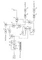
まず、図1に示すように、本実施形態の高周波回路装置において、送信用増幅回路を構成する高周波増幅器1、18は、それらの電源端子に電源振幅変調器10から振幅信号AS Txに応じた振幅変調電圧が供給され、基本的にポーラー変調またはポーラーループ変調動作を行う。
First, as shown in FIG. 1, in the high-frequency circuit device of the present embodiment, the high-
つまり、本実施形態は、従来の直交変調動作で実現した多数の送信信号帯域に対してそれぞれで動作する線形動作の高周波増幅器とアイソレータを用いる従来例に対して、まず、W-CDMA動作をすべてポーラー変調もしくはポーラーループ変調する。このために、高周波増幅器には位相信号が入力されて、さらに、電源端子に振幅変調電圧が入力される。これにより、従来の線形増幅器が不要となり、ポーラー変調動作の高周波増幅器は、飽和動作の高周波増幅器で実現できるため、非常に広帯域な高周波増幅器が実現される。 In other words, in this embodiment, first, all W-CDMA operations are performed with respect to the conventional example using a linear operation high-frequency amplifier and an isolator that operate for each of a number of transmission signal bands realized by a conventional quadrature modulation operation. Polar modulation or polar loop modulation. Therefore, a phase signal is input to the high frequency amplifier, and an amplitude modulation voltage is input to the power supply terminal. This eliminates the need for a conventional linear amplifier, and a high-frequency amplifier with polar modulation can be realized with a high-frequency amplifier with saturation operation, thereby realizing a very wide-band high-frequency amplifier.
さらに、ポーラー変調化するためには、現行の高周波化する半導体技術で高周波動作化する高周波振幅変調器10、また後述のアイソレータを削除する際に他の周波数への影響を避けるデュプレクサ(共用器)の設計により実現可能となる。
Furthermore, in order to achieve polar modulation, a high-
以下、本実施形態の高周波回路装置について具体的に説明する。 Hereinafter, the high-frequency circuit device of the present embodiment will be specifically described.
図1において、W-CDMA方式の800−900MHz帯の位相信号PS Tx(0.8)が高周波増幅器1により増幅される。一方、W-CDMA方式の1700から2100MHzの位相信号PS Tx(1.7−2)は、広帯域用の高周波増幅器18により増幅される。ポーラー変調あるいはポーラーループ変調のために、このような広帯域の高周波増幅器が飽和動作で実現可能となる。また、高周波増幅器1、18は、利得制御可能なドライバー増幅器5を内蔵し、W-CDMA方式のダイナミックレンジの拡大を行う。また、ポーラー変調のために高周波増幅器1、18の電源端子には、電源振幅変調器10から送信信号の振幅情報に応じた振幅変調電圧が入力される。
In FIG. 1, a 800-900 MHz band phase signal PS Tx (0.8) of the W-CDMA system is amplified by a high-
高周波増幅器18の出力信号は、前段のスイッチ回路21、21を介してデュプレクサ32、33に入力される。このデュプレクサは、送受信を同時に行うための周波数帯によって切り分けるフィルターである。アンテナ7が金属や人間の頭に近づきインピーダンスが50オームからずれて、高周波増幅器18のW-CDMA動作での歪特性が悪化するのはポーラー変調動作で避けることができる。これに加えて、他の携帯電話や基地局からの送信信号や受信信号がアンテナ7から高周波増幅器1や18に逆流して、他の周波数帯に妨害波を発生するなど悪影響を及ぼすのを避けるために、デュプレクサ31、32、33は、それぞれ800−900MHz帯あるいは900−1000MHz帯や1.7GHz帯や2GHz帯あるいは1.9−2GHz帯などの本来高周波増幅器からの信号を通過させるとき、前段のスイッチ回路21で選択されるが、送信帯域の信号から200MHz以上離れた信号を抑圧する遮断特性をも持たせることで、従来ではアイソレータが果たしたこの抑圧機能によりアイソレータを省略することを実現し、ポーラー変調化あるいはポーラーループ変調化できる。
The output signal of the
例えば、1.7GHz用のデュプレクサ33は、アンテナ7から入る1.4−1.5GHzの外部からの他の携帯電話送信信号を抑圧し、高周波増幅器18が出力する1.7GHz帯の送信信号と生じる2GHz帯周辺の妨害信号がアンテナ7から出て、他の携帯電話の2GHz帯の受信信号の妨害や送信信号の妨害にならないようにする。
For example, the
あるいは、例えば、1.7GHz用のデュプレクサ33は、アンテナ7から入る2−2.1GHzの外部からの他の携帯電話送信信号を抑圧し、高周波増幅器18が出力する1.7GHzの送信信号と生じる1.4−1.5GHz帯周辺の妨害信号がアンテナ7から出て、他の携帯電話の1.4−1.5GHz帯の受信信号の妨害や送信信号の妨害にならないようにする。
Alternatively, for example, a
さらに、デュプレクサ32、33とアンテナ7との間に、どの周波数帯域で送受信させるかの選択を行う後段のスイッチ回路(マルチスイッチ)8を設けて、切替可能な構成とする。これら前段のスイッチ回路21や後段のスイッチ回路8としてはGaAsの高周波スイッチ(SW)が用いられる。また、この高周波スイッチはピンダイオードで構成されることもある。また、高周波増幅器1、18からの高調波を抑圧するためにローパスフィルター(LPF)6が用いられる。高周波増幅器1、18は、GaAsのFETやHBT(ヘテロバイポーラトランジスタ)やSiGeのHBTで構成され、飽和アンプとしてもよいので、シリコンのMOS FETやバイポーラトランジスタが用いられることもある。
Further, a switch circuit (multi-switch) 8 is provided between the
受信時には、表面弾性波(SAW)フィルター11で周波数を限定するが、デュプレクサ31、32、33のフィルター特性を強めて、デュプレクサでSAWフィルターの役割を担うこともある。
At the time of reception, the frequency is limited by the surface acoustic wave (SAW)
以上のように、本実施形態によれば、図7に示す従来例2と比較して、高周波増幅回路の数を3個から2個に削減することができ、さらに、アイソレータも省けるので、コストが約半減できる。また、アイソレータが無いことでの出力損失低減とポーラー変調で飽和動作が可能になることで、W-CDMA等CDMA動作の高周波増幅器の電流を30%-80%程度も低減することができる。 As described above, according to this embodiment, the number of high-frequency amplifier circuits can be reduced from three to two as compared with the conventional example 2 shown in FIG. Can be halved. In addition, since the output loss can be reduced without the isolator and the saturation operation can be performed by the polar modulation, the current of the high-frequency amplifier for CDMA operation such as W-CDMA can be reduced by about 30% to 80%.
(第2の実施形態)
図2は、本発明の第2の実施形態に係る高周波回路装置の一構成例を示すブロック図である。
(Second Embodiment)
FIG. 2 is a block diagram showing a configuration example of the high-frequency circuit device according to the second embodiment of the present invention.
図2に示すように、本実施形態は、第1の実施形態に対して、さらに1.4GHzから1.5GHz帯の周波数帯域のW-CDMAを含む場合を想定している。本実施形態では、広帯域用の高周波増幅器を、さらに飽和特性を活かして広帯域化して1.5GHz−2GHz帯動作の高周波増幅器29とする。高周波増幅器29には、1.5−2GHz帯の位相信号PS Tx(1.5−2)が入力される。
As shown in FIG. 2, the present embodiment assumes a case in which W-CDMA in the frequency band from 1.4 GHz to 1.5 GHz is further included in the first embodiment. In the present embodiment, the high-frequency amplifier for a wide band is further widened by taking advantage of the saturation characteristics to obtain a high-
また、アンテナ7と高周波増幅器29との間には、デュプレクサ34が前段のスイッチ回路21と後段のスイッチ回路(マルチスイッチ)8に挟まれて設けられる。この際、1.5GHz用のデュプレクサ34は、アンテナ7から入る外部からの他の携帯電話の800−900MHz帯の送信信号を抑圧し、高周波増幅器29から出力される1.4−1.5GHzの送信信号と生じる2GHz周辺の妨害信号がアンテナ7から出て、他の携帯電話の2GHz帯の受信信号の妨害や送信信号の妨害にならないようにする。
In addition, a
以上のように、本実施形態によれば、従来では4つ必要であった高周波増幅器を2個に削減することができ、さらに、アイソレータも省けるので、コストが約1/3以下に低減できる。また、アイソレータが無いことでの出力損失低減とポーラー変調で飽和動作が可能になることで、W-CDMA等CDMA動作の高周波増幅器の電流を30%−80%程度も低減することができる。 As described above, according to the present embodiment, it is possible to reduce the number of high-frequency amplifiers conventionally required to four to two, and further, it is possible to omit an isolator, so that the cost can be reduced to about 3 or less. Further, since the saturation operation can be performed by the output loss reduction and the polar modulation without the isolator, the current of the CDMA operation high frequency amplifier such as W-CDMA can be reduced by about 30% to 80%.
(第3の実施形態)
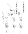
図3は、本発明の第3の実施形態に係る高周波回路装置の一構成例を示すブロック図である。
(Third embodiment)
FIG. 3 is a block diagram showing a configuration example of the high-frequency circuit device according to the third embodiment of the present invention.
まず、図3に示すように、本実施形態は、第1の実施形態と比較して、さらに800MHzから2GHz帯の周波数帯域のW-CDMAをすべて一つの高周波増幅器20で実現する場合を想定している。本実施形態では、高周波増幅器20の最終増幅段に帰還回路35を内蔵することで広帯域化して800MHz−2GHz動作を可能にしている。帰還回路35は通常、抵抗成分と直流カットの容量で構成される。高周波増幅器20には、800MHz−2GHz帯の位相信号PS Tx(0.8−2)が入力される。
First, as shown in FIG. 3, the present embodiment assumes a case where W-CDMA in a frequency band from 800 MHz to 2 GHz is further realized by a single high-
また、アンテナ7と高周波増幅器20との間には、各帯域のデュプレクサ31、32、33が、前段のスイッチ回路21と後段のスイッチ回路(マルチスイッチ)8に挟まれて設けられる。この際、各デュプレクサが、第1および第2の実施形態と同様に抑圧特性を持ち、他の携帯電話からの送信信号がアンテナ7から入力して妨害信号が高周波増幅器20で発生してアンテナ7から出ることを抑制する。
Also, between the
以上のように、本実施形態によれば、従来では3つ必要であった高周波増幅器を1個に削減できて、さらに、アイソレータも省けるので、コストを約1/4以下に低減できる。また、アイソレータが無いことでの出力損失低減とポーラー変調で飽和動作が可能になることで、W-CDMA等CDMA動作の高周波増幅器の電流を30%−80%程度も低減することができる。 As described above, according to the present embodiment, it is possible to reduce the number of high-frequency amplifiers that were conventionally required to one to one, and further to eliminate an isolator, so that the cost can be reduced to about ¼ or less. Further, since the saturation operation can be performed by the output loss reduction and the polar modulation without the isolator, the current of the CDMA operation high frequency amplifier such as W-CDMA can be reduced by about 30% to 80%.
なお、W-CDMAが2.5−2.7GHz帯まで拡張されるか、もしくは、TD-CDMAやTD-SCDMAになっても、800MHz−2.7GHzの高周波増幅器を用いることで同様に考えられるのは言うまでもない。 In addition, even if W-CDMA is expanded to 2.5-2.7GHz band, or it becomes TD-CDMA or TD-SCDMA, it can be similarly considered by using a high-frequency amplifier of 800MHz-2.7GHz. Needless to say.
(第4の実施形態)
図4は、本発明の第4の実施形態に係る高周波回路装置の一構成例を示すブロック図である。
(Fourth embodiment)
FIG. 4 is a block diagram showing a configuration example of the high-frequency circuit device according to the fourth embodiment of the present invention.
図3に示す第3の実施形態では、ローパスフィルター(LPF)23が1.7GHz帯や2GHz帯の送信信号の2倍、3倍の高調波成分を減衰させるために、約3GHz以上の信号を十分抑圧するが、1.7GHz帯と2GHz帯の送信信号が高周波増幅器20からデュプレクサ33、32に到達するまでに2個のスイッチ回路21を通過するので、損失が大きかった。
In the third embodiment shown in FIG. 3, a low-pass filter (LPF) 23 attenuates a harmonic component that is twice or three times that of a 1.7 GHz band or 2 GHz band transmission signal. Although sufficiently suppressed, since the 1.7 GHz band and 2 GHz band transmission signals pass through the two
そこで、本実施形態では、図4に示すように、1.7GHz帯と2GHz帯のローパスフィルター(LPF)24、23をそれぞれスイッチ回路21とデュプレクサ33、32との間に配置して、それぞれ1.7GHz帯や2GHz帯の送信信号の2倍、3倍の高調波成分を減衰させる特性を持たせた。これにより、1.7GHz帯と2GHz帯の送信信号が高周波増幅器20からデュプレクサ33、32に到達するまでに1個のスイッチ回路21しか通過しないので、損失を0.2dBから0.3dB小さくすることが出来る。
Therefore, in the present embodiment, as shown in FIG. 4, 1.7 GHz band and 2 GHz band low pass filters (LPF) 24 and 23 are arranged between the
以上のように、本実施形態によれば、従来では3つ必要であった高周波増幅器を1個に削減することができ、さらに、アイソレータも省けるので、コストを約1/4以下に低減できる。さらに、第3の実施形態に対して、1.7GHz帯と2GHz帯の高周波増幅器の出力損失を約10%低減できるので、さらに10%程度も高周波増幅器の電流を低減することができる。 As described above, according to the present embodiment, it is possible to reduce the number of high-frequency amplifiers that were conventionally required to one to one, and further to eliminate an isolator, so that the cost can be reduced to about ¼ or less. Furthermore, since the output loss of the 1.7 GHz band and 2 GHz band high frequency amplifiers can be reduced by about 10% compared to the third embodiment, the current of the high frequency amplifier can be further reduced by about 10%.
なお、第3および第4の実施形態では、1.4−1.5GHz帯のW-CDMAを用いないで説明したが、これを使用する場合は、図2に示すように、1.4−1.5GHz用のデュプレクサを含む回路を高周波増幅器とアンテナの間に追加することで実現できることは明らかである。 In the third and fourth embodiments, the description has been made without using 1.4-1.5 GHz band W-CDMA. However, when this is used, as shown in FIG. It is clear that this can be realized by adding a circuit including a 1.5 GHz duplexer between the high frequency amplifier and the antenna.
(第5の実施形態)
図5は、本発明の第5の実施形態に係る高周波回路装置の一構成例を示すブロック図である。
(Fifth embodiment)
FIG. 5 is a block diagram showing a configuration example of the high-frequency circuit device according to the fifth embodiment of the present invention.
図5に示すように、第1から第4の実施形態に対して、携帯電話にOFDM(Orthogonal Frequency Division Multiplex)などマルチキャリア変調した信号の無線LANの信号を本システムで送信する場合は、周波数と動作の違いから、出力がW-CDMA動作の携帯電話の送信出力より10分の1から100分の1であるが、これは、電源振幅変調器10の振幅幅で制御して実現すれば、ポーラー変調あるいはポーラーループ変調で同一の高周波増幅器を用いて実現できる。この際、本実施形態では、高周波増幅器30の出力信号を後段のスイッチ回路(マルチスイッチ)8に直接供給するワイヤレスLAN用送信信号路27を設けることで、マルチスイッチ28による切り替えで通信可能となる。さらに、ワイヤレスLAN用受信増幅器29がSAWフィルター11を介してマルチスイッチ8に接続され、これによりワイヤレスLAN受信時には、受信信号Rx(LAN)として受信される。
As shown in FIG. 5, in contrast to the first to fourth embodiments, when a wireless LAN signal of a multicarrier modulated signal such as OFDM (Orthogonal Frequency Division Multiplex) is transmitted to the mobile phone using this system, Because of the difference in operation, the output is one-tenth to one-hundredth that of the transmission output of a mobile phone operating in W-CDMA, but this can be realized by controlling with the amplitude width of the power
この際、1.7GHz用デュプレクサ33は、アンテナ7から入る外部からの他の携帯電話の800−900MHz帯あるいは900−1000MHz帯の送信信号を抑圧し、高周波増幅器30から出力される1.7GHz帯の送信信号と生じる2.4GHz周辺あるいは2.5GHz−2.7GHz帯の妨害信号がアンテナ7から出て、2.4GHz帯あるいは2.5GHz−2.7GHz帯の受信信号の妨害や送信信号の妨害にならないようにする。
In this case, 1.7 GHz for
また、2GHz用デュプレクサ32は、アンテナ7から入る外部からの他の携帯電話の1.4−1.5GHz帯の送信信号を抑圧し、高周波増幅器30から出力される2GHzの送信信号と生じる2.4GHz−2.5GHz帯周辺の妨害信号がアンテナ7から出て、2.4GHz−2.5GHz帯の受信信号の妨害や送信信号の妨害にならないようにする。つまり、2.4GHzの無線LANの受信信号/送信信号、さらに2.5GHz−2.7GHz帯のW-CDMA,TD-CDMA,TD-SCDMA等の受信信号/送信信号の妨害にならないようになる。
Further, 2GHz for
また、2.4GHz帯や5GHz帯の無線LAN機能の追加は周波数が離れているため、従来では、一つの高周波増幅器で実現することは困難であった。しかしながら、本実施形態によれば、従来では必要であった2.4GHz帯の無線LAN用の高周波増幅器を無くすことができる。 In addition, since the addition of the wireless LAN function in the 2.4 GHz band and the 5 GHz band is far away, it has conventionally been difficult to realize with one high frequency amplifier. However, according to the present embodiment, it is possible to eliminate the 2.4 GHz band high frequency amplifier for wireless LAN, which was necessary in the past.
ここではW-CDMAを中心に説明したが、複数帯域を用いるCDMA携帯電話やW-CDMAとCDMA共用機でも同様の効果があることは言うまでもない。 Here, W-CDMA has been mainly described, but it goes without saying that the same effect can be obtained in a CDMA mobile phone using multiple bands and a W-CDMA and CDMA shared machine.
本発明に係る高周波回路装置は、低コスト化(1/3から1/5)かつ低消費電力化(約20%削減)を図り、送信周波数帯を新たに追加しても高周波増幅器を別途設ける必要が無いという利点を有し、複数の周波数帯域を用いるW-CDMA携帯電話システム、800−900MHz、1.4−1.5GHz、1.6−1.8GHz、1.9−2.0GHz、2.5−2.7GHzの周波数帯域を用いるW-CDMA携帯電話に有用である。さらに、このW-CDMA携帯電話に2.4GHz帯の無線LAN機能が追加した多機能携帯電話に有用である。さらには、2.5−2.7GHz帯のW-CDMA,TD-CDMA,TD-SCDMAを追加した携帯電話に有効である。またさらに、複数帯域のCDMA携帯電話やW-CDMA,LAN,CDMAの混用携帯電話にも有効である。 The high-frequency circuit device according to the present invention achieves low cost (1/3 to 1/5) and low power consumption (about 20% reduction), and a high-frequency amplifier is additionally provided even if a new transmission frequency band is added W-CDMA mobile phone system using a plurality of frequency bands, having the advantage that there is no need, 800-900 MHz, 1.4-1.5 GHz, 1.6-1.8 GHz, 1.9-2.0 GHz, This is useful for a W-CDMA mobile phone using a frequency band of 2.5-2.7 GHz. Furthermore, it is useful for a multi-function mobile phone in which a 2.4 GHz band wireless LAN function is added to this W-CDMA mobile phone. Furthermore, it is effective for mobile phones to which 2.5-2.7 GHz band W-CDMA, TD-CDMA, and TD-SCDMA are added. Furthermore, it is also effective for multi-band CDMA mobile phones and mixed mobile phones for W-CDMA, LAN, and CDMA.
1 800MHz帯W-CDMA高周波増幅器
5 ドライバー増幅器
6 ローパスフィルター(LPF)
7 アンテナ
8、28 マルチスイッチ(後段のスイッチ回路)
10 電源振幅変調器
11 SAWフィルター
12 低雑音増幅器(LNA)
18 1.7−2GHz帯W-CDMA高周波増幅器
20 800MHz−2GHz帯W-CDMA高周波増幅器
21 前段のスイッチ回路
22 前段のスイッチ回路
23 ローパスフィルター(LPF)
24 ローパスフィルター(LPF)
27 ワイヤレスLAN用送信信号路
30 800MHz−2.5GHz帯W-CDMAかつ無線LAN用高周波増幅器
31 800−1000MHz帯用デュプレクサ
32 1.9−2.1GHz帯用デュプレクサ
33 1.7GHz帯用デュプレクサ
34 1.4−1.5GHz帯用デュプレクサ
35 帰還回路
1 800MHz band W-CDMA
7
10 Power
18 1.7-2GHz band W-CDMA high-
24 Low-pass filter (LPF)
27 Transmission Signal Path for
Claims (6)
200MHz以上離れた複数の送信周波数帯の信号を増幅する広帯域用の高周波増幅器を少なくとも1つ含み、高周波電力をアンテナから送信するための送信用増幅回路と、
前記複数の送信周波数帯に対応させて各々設けられ、同時送受信を実現する複数のデュプレクサと、
広帯域用の前記高周波増幅器と前記複数のデュプレクサの間に各々配置された前段のスイッチ回路と、
前記複数のデュプレクサと前記アンテナとの間に配置された後段のスイッチ回路と、
前記送信用増幅回路の電源端子に振幅変調電圧を供給する電源振幅変調器とを備え、
前記高周波増幅器は、信号入力端子に送信信号の位相情報が供給され、前記電源端子に前記電源振幅変調器から送信信号の振幅情報に応じた前記振幅変調電圧が供給され、ポーラー変調またはポーラーループ変調され、
同時送受信する周波数帯に応じて、対応する前記前段のスイッチ回路がオンになり、前記後段のスイッチ回路は対応する前記デュプレクサを前記アンテナに接続することを特徴とする高周波回路装置。 A high-frequency circuit device corresponding to a wideband code division multiple access (W-CDMA) or code division multiple access (CDMA) system in which a plurality of transmission frequency bands exist,
A transmission amplifying circuit for transmitting high-frequency power from an antenna, comprising at least one broadband high-frequency amplifier that amplifies signals in a plurality of transmission frequency bands separated by 200 MHz or more;
A plurality of duplexers that are respectively provided corresponding to the plurality of transmission frequency bands and realize simultaneous transmission and reception;
A front-stage switch circuit disposed between the high-frequency amplifier for broadband and the plurality of duplexers ;
And subsequent switching circuit disposed between said plurality of duplexer Sa and the antenna,
A power supply amplitude modulator that supplies an amplitude modulation voltage to a power supply terminal of the transmission amplifier circuit;
In the high-frequency amplifier, phase information of a transmission signal is supplied to a signal input terminal, and the amplitude modulation voltage corresponding to the amplitude information of the transmission signal is supplied to the power supply terminal from the power supply amplitude modulator. Polar modulation or polar loop modulation And
The high-frequency circuit device according to claim 1, wherein the corresponding switch circuit in the preceding stage is turned on according to a frequency band for simultaneous transmission and reception, and the switch circuit in the subsequent stage connects the corresponding duplexer to the antenna .
Priority Applications (7)
| Application Number | Priority Date | Filing Date | Title |
|---|---|---|---|
| JP2004054631A JP3961498B2 (en) | 2004-02-27 | 2004-02-27 | High frequency circuit equipment |
| TW094103935A TW200533096A (en) | 2004-02-27 | 2005-02-05 | High-frequency circuit device |
| US11/058,853 US20050191973A1 (en) | 2004-02-27 | 2005-02-15 | High-frequency circuit device |
| EP05251118A EP1569353A3 (en) | 2004-02-27 | 2005-02-25 | High frequency circuit device |
| CN2005100524775A CN1661935A (en) | 2004-02-27 | 2005-02-28 | High-frequency circuit device |
| KR1020050016886A KR20060043287A (en) | 2004-02-27 | 2005-02-28 | High-frequency circuit device |
| US12/152,803 US7706835B2 (en) | 2004-02-27 | 2008-05-16 | High-frequency circuit device |
Applications Claiming Priority (1)
| Application Number | Priority Date | Filing Date | Title |
|---|---|---|---|
| JP2004054631A JP3961498B2 (en) | 2004-02-27 | 2004-02-27 | High frequency circuit equipment |
Publications (2)
| Publication Number | Publication Date |
|---|---|
| JP2005244826A JP2005244826A (en) | 2005-09-08 |
| JP3961498B2 true JP3961498B2 (en) | 2007-08-22 |
Family
ID=34747568
Family Applications (1)
| Application Number | Title | Priority Date | Filing Date |
|---|---|---|---|
| JP2004054631A Expired - Fee Related JP3961498B2 (en) | 2004-02-27 | 2004-02-27 | High frequency circuit equipment |
Country Status (6)
| Country | Link |
|---|---|
| US (2) | US20050191973A1 (en) |
| EP (1) | EP1569353A3 (en) |
| JP (1) | JP3961498B2 (en) |
| KR (1) | KR20060043287A (en) |
| CN (1) | CN1661935A (en) |
| TW (1) | TW200533096A (en) |
Families Citing this family (15)
| Publication number | Priority date | Publication date | Assignee | Title |
|---|---|---|---|---|
| US8884714B2 (en) * | 2005-12-22 | 2014-11-11 | Pine Valley Investments, Inc. | Apparatus, system, and method for digital base modulation of power amplifier in polar transmitter |
| JP2008154201A (en) * | 2006-07-07 | 2008-07-03 | Murata Mfg Co Ltd | Transmitter |
| WO2008081632A1 (en) * | 2006-12-27 | 2008-07-10 | Panasonic Corporation | Polar-modulation transmission device |
| KR100930585B1 (en) * | 2007-10-05 | 2009-12-09 | 한국전자통신연구원 | Multiband Signal Separation Conversion Method and Apparatus |
| JP5504569B2 (en) * | 2008-03-24 | 2014-05-28 | 日本電気株式会社 | Receiving machine |
| JPWO2012102284A1 (en) * | 2011-01-28 | 2014-06-30 | 株式会社村田製作所 | Transmission module |
| US8861407B2 (en) * | 2011-07-07 | 2014-10-14 | Provigent Ltd. | Multiple connection options for a transceiver |
| JP6119735B2 (en) | 2012-03-12 | 2017-04-26 | 日本電気株式会社 | Transmitting apparatus and transmitting method |
| WO2014054786A1 (en) | 2012-10-05 | 2014-04-10 | 日本電気株式会社 | Transmission apparatus and transmission method |
| CA2814303A1 (en) | 2013-04-26 | 2014-10-26 | Cellphone-Mate, Inc. | Apparatus and methods for radio frequency signal boosters |
| US9362988B2 (en) * | 2014-10-28 | 2016-06-07 | Qualcomm Incorporated | WWAN and WLAN cooperative support of multi-SIM devices |
| JP2017011533A (en) * | 2015-06-23 | 2017-01-12 | 株式会社村田製作所 | Communication unit |
| KR20170053484A (en) * | 2015-11-06 | 2017-05-16 | 삼성전자주식회사 | Method for Processing Signal and Electronic Device supporting the same |
| CN105490699B (en) * | 2015-12-24 | 2019-01-22 | 中国电子科技集团公司第五十四研究所 | A kind of highly integrated communication unit circuit |
| CN111082814A (en) * | 2019-12-13 | 2020-04-28 | 惠州Tcl移动通信有限公司 | Method and device for downlink signal transmission in dual-connection architecture, and terminal |
Family Cites Families (32)
| Publication number | Priority date | Publication date | Assignee | Title |
|---|---|---|---|---|
| JPS61105101A (en) | 1984-10-29 | 1986-05-23 | Kokusai Electric Co Ltd | High efficiency ssb transmitter |
| US4972440A (en) * | 1988-09-23 | 1990-11-20 | Hughes Aircraft Company | Transmitter circuit for efficiently transmitting communication traffic via phase modulated carrier signals |
| JPH0787303B2 (en) | 1989-12-27 | 1995-09-20 | 三菱電機株式会社 | High frequency amplifier |
| JP2540377B2 (en) * | 1990-07-04 | 1996-10-02 | 三菱電機株式会社 | Automatic output power controller |
| US5689817A (en) * | 1996-01-26 | 1997-11-18 | Lucent Technologies Inc. | RF duplexer bypassing techniques for transceivers |
| JP3241594B2 (en) * | 1996-04-08 | 2001-12-25 | 松下電器産業株式会社 | Multi-band mobile radio equipment |
| US6298244B1 (en) | 1997-07-03 | 2001-10-02 | Ericsson Inc. | Dual-band, dual-mode power amplifier |
| JP3848445B2 (en) * | 1997-09-26 | 2006-11-22 | 松下電器産業株式会社 | Radio equipment compatible with multiple communication systems |
| JP3629136B2 (en) * | 1998-02-27 | 2005-03-16 | 富士通株式会社 | Multi-mode communication device |
| US6101224A (en) * | 1998-10-07 | 2000-08-08 | Telefonaktiebolaget Lm Ericsson | Method and apparatus for generating a linearly modulated signal using polar modulation |
| US6590940B1 (en) | 1999-05-17 | 2003-07-08 | Ericsson Inc. | Power modulation systems and methods that separately amplify low and high frequency portions of an amplitude waveform |
| TW512631B (en) * | 1999-05-24 | 2002-12-01 | Sharp Kk | Signal distribution circuit |
| JP3600115B2 (en) * | 2000-04-05 | 2004-12-08 | 株式会社東芝 | High frequency circuit and communication system |
| US6567653B1 (en) * | 2000-04-12 | 2003-05-20 | Ericsson Inc. | Dual-mode communications transmitter |
| US6992990B2 (en) * | 2000-07-17 | 2006-01-31 | Sony Corporation | Radio communication apparatus |
| JP2002135157A (en) * | 2000-10-20 | 2002-05-10 | Sony Corp | Multi-band portable radio terminal |
| DE10053205B4 (en) * | 2000-10-26 | 2017-04-13 | Epcos Ag | Combined front-end circuit for wireless transmission systems |
| DE10056472A1 (en) * | 2000-11-15 | 2002-05-29 | Infineon Technologies Ag | Polar loop transmission circuit has oscillator producing HF signal depending on phase comparison, amplitude modulator, feedback path, amplifier between amplitude modulator, mixer |
| JP2002208869A (en) | 2001-01-09 | 2002-07-26 | Sony Corp | Multiband radio signal transmission/reception device |
| JP2002325049A (en) * | 2001-04-26 | 2002-11-08 | Hitachi Ltd | Communication terminal sharable by different communication systems, antenna duplexer and power amplifier for use therein |
| US6665525B2 (en) * | 2001-05-29 | 2003-12-16 | Ericsson Inc. | High-level modulation method and apparatus |
| KR20040078699A (en) * | 2002-02-20 | 2004-09-10 | 코닌클리즈케 필립스 일렉트로닉스 엔.브이. | Mobile multimode terminal with joint power amplifier |
| GB2412513B (en) * | 2002-05-31 | 2006-03-08 | Renesas Tech Corp | Apparatus for radio telecommunication system and method of building up output power |
| WO2004002098A1 (en) | 2002-06-19 | 2003-12-31 | Hitachi, Ltd. | Radio communication apparatus |
| US6906592B2 (en) * | 2002-11-13 | 2005-06-14 | Qualcomm Inc | Continuously variable gain radio frequency driver amplifier having linear in decibel gain control characteristics |
| JPWO2005011109A1 (en) * | 2003-07-25 | 2006-09-14 | 松下電器産業株式会社 | Amplification equipment |
| GB2404506B (en) * | 2003-07-31 | 2006-02-22 | Renesas Tech Corp | Method of ramping up output level of power amplifier of radio communication system,communication semiconductor integrated circuit,& radio communication system |
| JP3961494B2 (en) * | 2004-02-18 | 2007-08-22 | 松下電器産業株式会社 | High frequency circuit equipment |
| US7157985B2 (en) * | 2004-03-15 | 2007-01-02 | Matsushita Electric Industrial Co., Ltd. | PLL modulation circuit and polar modulation apparatus |
| US7215215B2 (en) * | 2004-03-15 | 2007-05-08 | Matsushita Electric Industrial Co., Ltd. | Phase modulation apparatus, polar modulation transmission apparatus, wireless transmission apparatus and wireless communication apparatus |
| JP4628142B2 (en) * | 2005-03-03 | 2011-02-09 | パナソニック株式会社 | Polar modulation transmitter, wireless communication device, and power supply voltage control method |
| US7565118B2 (en) * | 2005-09-08 | 2009-07-21 | Panasonic Corporation | Polar modulation transmission apparatus and wireless communication apparatus |
-
2004
- 2004-02-27 JP JP2004054631A patent/JP3961498B2/en not_active Expired - Fee Related
-
2005
- 2005-02-05 TW TW094103935A patent/TW200533096A/en unknown
- 2005-02-15 US US11/058,853 patent/US20050191973A1/en not_active Abandoned
- 2005-02-25 EP EP05251118A patent/EP1569353A3/en not_active Withdrawn
- 2005-02-28 KR KR1020050016886A patent/KR20060043287A/en not_active Application Discontinuation
- 2005-02-28 CN CN2005100524775A patent/CN1661935A/en active Pending
-
2008
- 2008-05-16 US US12/152,803 patent/US7706835B2/en not_active Expired - Fee Related
Also Published As
| Publication number | Publication date |
|---|---|
| EP1569353A2 (en) | 2005-08-31 |
| TW200533096A (en) | 2005-10-01 |
| KR20060043287A (en) | 2006-05-15 |
| US20050191973A1 (en) | 2005-09-01 |
| US20080233899A1 (en) | 2008-09-25 |
| JP2005244826A (en) | 2005-09-08 |
| CN1661935A (en) | 2005-08-31 |
| US7706835B2 (en) | 2010-04-27 |
| EP1569353A3 (en) | 2008-01-02 |
Similar Documents
| Publication | Publication Date | Title |
|---|---|---|
| US7706835B2 (en) | High-frequency circuit device | |
| US6188877B1 (en) | Dual-band, dual-mode power amplifier with reduced power loss | |
| US8359067B2 (en) | Radio frequency device and mobile communication terminal using the same | |
| US6298244B1 (en) | Dual-band, dual-mode power amplifier | |
| US8502599B2 (en) | System and method for a multi-band power-amplifier | |
| US8643449B2 (en) | Impedance matching circuit capable of efficiently isolating paths for multi-band power amplifier | |
| US7689187B2 (en) | Dual input low noise amplifier for multi-band operation | |
| CN212935883U (en) | High-frequency circuit and communication device | |
| JP2021525482A (en) | Wideband Low Noise Amplifier (LNA) with Reconfigurable Bandwidth for Millimeter Wave 5G Communication | |
| JP2006166277A (en) | Transmission/reception apparatus and module | |
| JP2006521060A (en) | Radio frequency (RF) amplifier resistant to load fluctuations | |
| KR101131272B1 (en) | Input matching circuit for multiband low noise amplifier | |
| JP2006186596A (en) | Antenna duplexer and wireless communication terminal using the same | |
| US6798294B2 (en) | Amplifier with multiple inputs | |
| WO2001005028A1 (en) | A dual-band, dual-mode power amplifier | |
| CN113169749B (en) | Front end module and communication device | |
| JP3816356B2 (en) | Wireless transmitter | |
| US7269156B2 (en) | High-frequency circuit device | |
| JP4641021B2 (en) | Multiband radio and semiconductor integrated circuit | |
| US6711392B1 (en) | Balanced power amplifier for low power radio communications | |
| US7228110B2 (en) | Low cost high frequency device having compact mounting area, high frequency amplification method, wireless communication device and mobile telephone including low cost and high frequency circuit having compact mounting area | |
| JP2008205821A (en) | High-frequency power amplifier and transmitter using it | |
| JP2011199372A (en) | Multimode correspondence high frequency integrated circuit, portable terminal device, and other mode sneak preventing method | |
| JP2021528900A (en) | Wireless unit for asynchronous TDD multiband operation | |
| US20220255574A1 (en) | Front end module with switchable filter |
Legal Events
| Date | Code | Title | Description |
|---|---|---|---|
| A977 | Report on retrieval |
Free format text: JAPANESE INTERMEDIATE CODE: A971007 Effective date: 20061005 |
|
| A131 | Notification of reasons for refusal |
Free format text: JAPANESE INTERMEDIATE CODE: A131 Effective date: 20061026 |
|
| A521 | Written amendment |
Free format text: JAPANESE INTERMEDIATE CODE: A523 Effective date: 20061225 |
|
| A131 | Notification of reasons for refusal |
Free format text: JAPANESE INTERMEDIATE CODE: A131 Effective date: 20070123 |
|
| A521 | Written amendment |
Free format text: JAPANESE INTERMEDIATE CODE: A523 Effective date: 20070326 |
|
| TRDD | Decision of grant or rejection written | ||
| A01 | Written decision to grant a patent or to grant a registration (utility model) |
Free format text: JAPANESE INTERMEDIATE CODE: A01 Effective date: 20070417 |
|
| A61 | First payment of annual fees (during grant procedure) |
Free format text: JAPANESE INTERMEDIATE CODE: A61 Effective date: 20070516 |
|
| R150 | Certificate of patent or registration of utility model |
Free format text: JAPANESE INTERMEDIATE CODE: R150 |
|
| FPAY | Renewal fee payment (event date is renewal date of database) |
Free format text: PAYMENT UNTIL: 20110525 Year of fee payment: 4 |
|
| FPAY | Renewal fee payment (event date is renewal date of database) |
Free format text: PAYMENT UNTIL: 20110525 Year of fee payment: 4 |
|
| FPAY | Renewal fee payment (event date is renewal date of database) |
Free format text: PAYMENT UNTIL: 20120525 Year of fee payment: 5 |
|
| FPAY | Renewal fee payment (event date is renewal date of database) |
Free format text: PAYMENT UNTIL: 20120525 Year of fee payment: 5 |
|
| FPAY | Renewal fee payment (event date is renewal date of database) |
Free format text: PAYMENT UNTIL: 20130525 Year of fee payment: 6 |
|
| LAPS | Cancellation because of no payment of annual fees |