JP2024505507A - プラズマエッチング技法 - Google Patents
プラズマエッチング技法 Download PDFInfo
- Publication number
- JP2024505507A JP2024505507A JP2023545747A JP2023545747A JP2024505507A JP 2024505507 A JP2024505507 A JP 2024505507A JP 2023545747 A JP2023545747 A JP 2023545747A JP 2023545747 A JP2023545747 A JP 2023545747A JP 2024505507 A JP2024505507 A JP 2024505507A
- Authority
- JP
- Japan
- Prior art keywords
- layer
- plasma
- germanium
- containing layer
- gas
- Prior art date
- Legal status (The legal status is an assumption and is not a legal conclusion. Google has not performed a legal analysis and makes no representation as to the accuracy of the status listed.)
- Pending
Links
Images


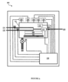
Classifications
-
- H—ELECTRICITY
- H01—ELECTRIC ELEMENTS
- H01J—ELECTRIC DISCHARGE TUBES OR DISCHARGE LAMPS
- H01J37/00—Discharge tubes with provision for introducing objects or material to be exposed to the discharge, e.g. for the purpose of examination or processing thereof
- H01J37/32—Gas-filled discharge tubes
- H01J37/32431—Constructional details of the reactor
- H01J37/3244—Gas supply means
- H01J37/32449—Gas control, e.g. control of the gas flow
-
- H—ELECTRICITY
- H10—SEMICONDUCTOR DEVICES; ELECTRIC SOLID-STATE DEVICES NOT OTHERWISE PROVIDED FOR
- H10P—GENERIC PROCESSES OR APPARATUS FOR THE MANUFACTURE OR TREATMENT OF DEVICES COVERED BY CLASS H10
- H10P50/00—Etching of wafers, substrates or parts of devices
- H10P50/20—Dry etching; Plasma etching; Reactive-ion etching
- H10P50/24—Dry etching; Plasma etching; Reactive-ion etching of semiconductor materials
- H10P50/242—Dry etching; Plasma etching; Reactive-ion etching of semiconductor materials of Group IV materials
-
- H—ELECTRICITY
- H10—SEMICONDUCTOR DEVICES; ELECTRIC SOLID-STATE DEVICES NOT OTHERWISE PROVIDED FOR
- H10D—INORGANIC ELECTRIC SEMICONDUCTOR DEVICES
- H10D30/00—Field-effect transistors [FET]
- H10D30/01—Manufacture or treatment
- H10D30/014—Manufacture or treatment of FETs having zero-dimensional [0D] or one-dimensional [1D] channels, e.g. quantum wire FETs, single-electron transistors [SET] or Coulomb blockade transistors
-
- H—ELECTRICITY
- H10—SEMICONDUCTOR DEVICES; ELECTRIC SOLID-STATE DEVICES NOT OTHERWISE PROVIDED FOR
- H10D—INORGANIC ELECTRIC SEMICONDUCTOR DEVICES
- H10D30/00—Field-effect transistors [FET]
- H10D30/40—FETs having zero-dimensional [0D], one-dimensional [1D] or two-dimensional [2D] charge carrier gas channels
- H10D30/43—FETs having zero-dimensional [0D], one-dimensional [1D] or two-dimensional [2D] charge carrier gas channels having one-dimensional [1D] charge carrier gas channels, e.g. quantum wire FETs or transistors having 1D quantum-confined channels
-
- H—ELECTRICITY
- H10—SEMICONDUCTOR DEVICES; ELECTRIC SOLID-STATE DEVICES NOT OTHERWISE PROVIDED FOR
- H10D—INORGANIC ELECTRIC SEMICONDUCTOR DEVICES
- H10D62/00—Semiconductor bodies, or regions thereof, of devices having potential barriers
- H10D62/10—Shapes, relative sizes or dispositions of the regions of the semiconductor bodies; Shapes of the semiconductor bodies
- H10D62/117—Shapes of semiconductor bodies
- H10D62/118—Nanostructure semiconductor bodies
- H10D62/119—Nanowire, nanosheet or nanotube semiconductor bodies
- H10D62/121—Nanowire, nanosheet or nanotube semiconductor bodies oriented parallel to substrates
-
- H—ELECTRICITY
- H10—SEMICONDUCTOR DEVICES; ELECTRIC SOLID-STATE DEVICES NOT OTHERWISE PROVIDED FOR
- H10P—GENERIC PROCESSES OR APPARATUS FOR THE MANUFACTURE OR TREATMENT OF DEVICES COVERED BY CLASS H10
- H10P14/00—Formation of materials, e.g. in the shape of layers or pillars
- H10P14/20—Formation of materials, e.g. in the shape of layers or pillars of semiconductor materials
- H10P14/29—Formation of materials, e.g. in the shape of layers or pillars of semiconductor materials characterised by the substrates
- H10P14/2901—Materials
- H10P14/2902—Materials being Group IVA materials
- H10P14/2905—Silicon, silicon germanium or germanium
-
- H—ELECTRICITY
- H10—SEMICONDUCTOR DEVICES; ELECTRIC SOLID-STATE DEVICES NOT OTHERWISE PROVIDED FOR
- H10P—GENERIC PROCESSES OR APPARATUS FOR THE MANUFACTURE OR TREATMENT OF DEVICES COVERED BY CLASS H10
- H10P14/00—Formation of materials, e.g. in the shape of layers or pillars
- H10P14/60—Formation of materials, e.g. in the shape of layers or pillars of insulating materials
- H10P14/63—Formation of materials, e.g. in the shape of layers or pillars of insulating materials characterised by the formation processes
- H10P14/6302—Non-deposition formation processes
- H10P14/6316—Formation by nitridation, e.g. nitridation of the substrate
-
- H—ELECTRICITY
- H10—SEMICONDUCTOR DEVICES; ELECTRIC SOLID-STATE DEVICES NOT OTHERWISE PROVIDED FOR
- H10P—GENERIC PROCESSES OR APPARATUS FOR THE MANUFACTURE OR TREATMENT OF DEVICES COVERED BY CLASS H10
- H10P14/00—Formation of materials, e.g. in the shape of layers or pillars
- H10P14/60—Formation of materials, e.g. in the shape of layers or pillars of insulating materials
- H10P14/63—Formation of materials, e.g. in the shape of layers or pillars of insulating materials characterised by the formation processes
- H10P14/6302—Non-deposition formation processes
- H10P14/6319—Formation by plasma treatments, e.g. plasma oxidation of the substrate
-
- H—ELECTRICITY
- H10—SEMICONDUCTOR DEVICES; ELECTRIC SOLID-STATE DEVICES NOT OTHERWISE PROVIDED FOR
- H10P—GENERIC PROCESSES OR APPARATUS FOR THE MANUFACTURE OR TREATMENT OF DEVICES COVERED BY CLASS H10
- H10P50/00—Etching of wafers, substrates or parts of devices
- H10P50/20—Dry etching; Plasma etching; Reactive-ion etching
- H10P50/28—Dry etching; Plasma etching; Reactive-ion etching of insulating materials
- H10P50/282—Dry etching; Plasma etching; Reactive-ion etching of insulating materials of inorganic materials
- H10P50/283—Dry etching; Plasma etching; Reactive-ion etching of insulating materials of inorganic materials by chemical means
-
- H—ELECTRICITY
- H10—SEMICONDUCTOR DEVICES; ELECTRIC SOLID-STATE DEVICES NOT OTHERWISE PROVIDED FOR
- H10P—GENERIC PROCESSES OR APPARATUS FOR THE MANUFACTURE OR TREATMENT OF DEVICES COVERED BY CLASS H10
- H10P70/00—Cleaning of wafers, substrates or parts of devices
- H10P70/20—Cleaning during device manufacture
-
- B—PERFORMING OPERATIONS; TRANSPORTING
- B82—NANOTECHNOLOGY
- B82Y—SPECIFIC USES OR APPLICATIONS OF NANOSTRUCTURES; MEASUREMENT OR ANALYSIS OF NANOSTRUCTURES; MANUFACTURE OR TREATMENT OF NANOSTRUCTURES
- B82Y10/00—Nanotechnology for information processing, storage or transmission, e.g. quantum computing or single electron logic
-
- B—PERFORMING OPERATIONS; TRANSPORTING
- B82—NANOTECHNOLOGY
- B82Y—SPECIFIC USES OR APPLICATIONS OF NANOSTRUCTURES; MEASUREMENT OR ANALYSIS OF NANOSTRUCTURES; MANUFACTURE OR TREATMENT OF NANOSTRUCTURES
- B82Y40/00—Manufacture or treatment of nanostructures
-
- H—ELECTRICITY
- H01—ELECTRIC ELEMENTS
- H01J—ELECTRIC DISCHARGE TUBES OR DISCHARGE LAMPS
- H01J2237/00—Discharge tubes exposing object to beam, e.g. for analysis treatment, etching, imaging
- H01J2237/32—Processing objects by plasma generation
- H01J2237/33—Processing objects by plasma generation characterised by the type of processing
- H01J2237/334—Etching
- H01J2237/3343—Problems associated with etching
- H01J2237/3346—Selectivity
-
- H—ELECTRICITY
- H10—SEMICONDUCTOR DEVICES; ELECTRIC SOLID-STATE DEVICES NOT OTHERWISE PROVIDED FOR
- H10D—INORGANIC ELECTRIC SEMICONDUCTOR DEVICES
- H10D30/00—Field-effect transistors [FET]
- H10D30/60—Insulated-gate field-effect transistors [IGFET]
- H10D30/67—Thin-film transistors [TFT]
- H10D30/6729—Thin-film transistors [TFT] characterised by the electrodes
- H10D30/673—Thin-film transistors [TFT] characterised by the electrodes characterised by the shapes, relative sizes or dispositions of the gate electrodes
- H10D30/6735—Thin-film transistors [TFT] characterised by the electrodes characterised by the shapes, relative sizes or dispositions of the gate electrodes having gates fully surrounding the channels, e.g. gate-all-around
-
- H—ELECTRICITY
- H10—SEMICONDUCTOR DEVICES; ELECTRIC SOLID-STATE DEVICES NOT OTHERWISE PROVIDED FOR
- H10D—INORGANIC ELECTRIC SEMICONDUCTOR DEVICES
- H10D30/00—Field-effect transistors [FET]
- H10D30/60—Insulated-gate field-effect transistors [IGFET]
- H10D30/67—Thin-film transistors [TFT]
- H10D30/6757—Thin-film transistors [TFT] characterised by the structure of the channel, e.g. transverse or longitudinal shape or doping profile
Landscapes
- Physics & Mathematics (AREA)
- Engineering & Computer Science (AREA)
- Plasma & Fusion (AREA)
- Chemical & Material Sciences (AREA)
- Analytical Chemistry (AREA)
- Drying Of Semiconductors (AREA)
- Insulated Gate Type Field-Effect Transistor (AREA)
Applications Claiming Priority (3)
| Application Number | Priority Date | Filing Date | Title |
|---|---|---|---|
| US17/161,199 | 2021-01-28 | ||
| US17/161,199 US11482423B2 (en) | 2021-01-28 | 2021-01-28 | Plasma etching techniques |
| PCT/US2022/013558 WO2022164759A1 (en) | 2021-01-28 | 2022-01-24 | Plasma etching techniques |
Publications (2)
| Publication Number | Publication Date |
|---|---|
| JP2024505507A true JP2024505507A (ja) | 2024-02-06 |
| JP2024505507A5 JP2024505507A5 (https=) | 2025-01-28 |
Family
ID=82496031
Family Applications (1)
| Application Number | Title | Priority Date | Filing Date |
|---|---|---|---|
| JP2023545747A Pending JP2024505507A (ja) | 2021-01-28 | 2022-01-24 | プラズマエッチング技法 |
Country Status (6)
| Country | Link |
|---|---|
| US (1) | US11482423B2 (https=) |
| JP (1) | JP2024505507A (https=) |
| KR (1) | KR20230131945A (https=) |
| CN (1) | CN116897414A (https=) |
| TW (1) | TW202238717A (https=) |
| WO (1) | WO2022164759A1 (https=) |
Families Citing this family (3)
| Publication number | Priority date | Publication date | Assignee | Title |
|---|---|---|---|---|
| US12272558B2 (en) * | 2022-05-09 | 2025-04-08 | Tokyo Electron Limited | Selective and isotropic etch of silicon over silicon-germanium alloys and dielectrics; via new chemistry and surface modification |
| WO2025174546A1 (en) * | 2024-02-12 | 2025-08-21 | Applied Materials, Inc. | Selective etching of silicon-and-germanium-containing materials with reduced under layer loss |
| WO2025244994A1 (en) * | 2024-05-21 | 2025-11-27 | Lam Research Corporation | Selective etch of stack using a nitrogen and fluorine containing gas |
Citations (4)
| Publication number | Priority date | Publication date | Assignee | Title |
|---|---|---|---|---|
| JP2013225604A (ja) * | 2012-04-23 | 2013-10-31 | Hitachi High-Technologies Corp | ドライエッチング方法 |
| US20150126039A1 (en) * | 2013-11-04 | 2015-05-07 | Applied Materials, Inc. | Etch suppression with germanium |
| JP2016143781A (ja) * | 2015-02-03 | 2016-08-08 | 東京エレクトロン株式会社 | エッチング方法 |
| US20200266070A1 (en) * | 2019-02-20 | 2020-08-20 | Tokyo Electron Limited | Method for Selective Etching at an Interface Between Materials |
Family Cites Families (11)
| Publication number | Priority date | Publication date | Assignee | Title |
|---|---|---|---|---|
| US6596597B2 (en) * | 2001-06-12 | 2003-07-22 | International Business Machines Corporation | Method of manufacturing dual gate logic devices |
| US8389416B2 (en) * | 2010-11-22 | 2013-03-05 | Tokyo Electron Limited | Process for etching silicon with selectivity to silicon-germanium |
| JP5851349B2 (ja) | 2012-06-04 | 2016-02-03 | 株式会社日立ハイテクノロジーズ | プラズマエッチング方法及びプラズマエッチング装置 |
| US9419107B2 (en) | 2014-06-19 | 2016-08-16 | Applied Materials, Inc. | Method for fabricating vertically stacked nanowires for semiconductor applications |
| US9653291B2 (en) * | 2014-11-13 | 2017-05-16 | Applied Materials, Inc. | Method for removing native oxide and residue from a III-V group containing surface |
| US9786664B2 (en) * | 2016-02-10 | 2017-10-10 | International Business Machines Corporation | Fabricating a dual gate stack of a CMOS structure |
| KR102323389B1 (ko) | 2016-03-02 | 2021-11-05 | 도쿄엘렉트론가부시키가이샤 | 튜닝가능한 선택도를 갖는 등방성 실리콘 및 실리콘-게르마늄 에칭 |
| US10177227B1 (en) * | 2017-08-28 | 2019-01-08 | Applied Materials, Inc. | Method for fabricating junctions and spacers for horizontal gate all around devices |
| US10529581B2 (en) * | 2017-12-29 | 2020-01-07 | L'Air Liquide, Société Anonyme pour l'Etude et l'Exploitation des Procédés Georges Claude | SiN selective etch to SiO2 with non-plasma dry process for 3D NAND device applications |
| KR102727230B1 (ko) * | 2019-07-18 | 2024-11-06 | 도쿄엘렉트론가부시키가이샤 | 금속의 제어 가능한 에칭 선택비를 갖는 기상 에칭 |
| US11069819B2 (en) * | 2019-10-30 | 2021-07-20 | Globalfoundries U.S. Inc. | Field-effect transistors with channel regions that include a two-dimensional material on a mandrel |
-
2021
- 2021-01-28 US US17/161,199 patent/US11482423B2/en active Active
-
2022
- 2022-01-24 CN CN202280017300.3A patent/CN116897414A/zh active Pending
- 2022-01-24 JP JP2023545747A patent/JP2024505507A/ja active Pending
- 2022-01-24 KR KR1020237028670A patent/KR20230131945A/ko active Pending
- 2022-01-24 WO PCT/US2022/013558 patent/WO2022164759A1/en not_active Ceased
- 2022-01-27 TW TW111103598A patent/TW202238717A/zh unknown
Patent Citations (4)
| Publication number | Priority date | Publication date | Assignee | Title |
|---|---|---|---|---|
| JP2013225604A (ja) * | 2012-04-23 | 2013-10-31 | Hitachi High-Technologies Corp | ドライエッチング方法 |
| US20150126039A1 (en) * | 2013-11-04 | 2015-05-07 | Applied Materials, Inc. | Etch suppression with germanium |
| JP2016143781A (ja) * | 2015-02-03 | 2016-08-08 | 東京エレクトロン株式会社 | エッチング方法 |
| US20200266070A1 (en) * | 2019-02-20 | 2020-08-20 | Tokyo Electron Limited | Method for Selective Etching at an Interface Between Materials |
Also Published As
| Publication number | Publication date |
|---|---|
| TW202238717A (zh) | 2022-10-01 |
| US20220238344A1 (en) | 2022-07-28 |
| KR20230131945A (ko) | 2023-09-14 |
| CN116897414A (zh) | 2023-10-17 |
| US11482423B2 (en) | 2022-10-25 |
| WO2022164759A1 (en) | 2022-08-04 |
Similar Documents
| Publication | Publication Date | Title |
|---|---|---|
| JP7812042B2 (ja) | プラズマエッチング技術 | |
| US11837467B2 (en) | Plasma etching techniques | |
| US9570317B2 (en) | Microelectronic method for etching a layer | |
| CN108573866B (zh) | 氧化膜去除方法和装置以及接触部形成方法和系统 | |
| TWI625785B (zh) | 具有可調節選擇性之等向性矽與矽化鍺蝕刻 | |
| US9093389B2 (en) | Method of patterning a silicon nitride dielectric film | |
| CN104008994B (zh) | 半导体装置的制造方法 | |
| US20140187046A1 (en) | Method for forming spacers for a transitor gate | |
| JP2024505507A (ja) | プラズマエッチング技法 | |
| US9947768B2 (en) | Method for forming spacers for a transistor gate | |
| JP2018148193A (ja) | 酸化膜除去方法および除去装置、ならびにコンタクト形成方法およびコンタクト形成システム | |
| CN108321090A (zh) | 半导体器件及其形成方法 | |
| US9780000B2 (en) | Method for forming spacers for a transitor gate | |
| US9773674B2 (en) | Method for forming patterns by implanting | |
| JP2025517645A (ja) | 新規な化学及び表面改質による、シリコン-ゲルマニウム合金ならびに誘電体を超えるシリコンの選択的及び等方性エッチング | |
| TWI913411B (zh) | 電漿蝕刻方法 | |
| JP2026513040A (ja) | 表面純度が上がったシリコンとゲルマニウムとを含有する材料の選択的エッチング | |
| TWI913396B (zh) | 電漿蝕刻技術 | |
| CN100459053C (zh) | 半导体器件栅极结构的制造方法 | |
| TWI767085B (zh) | 相對其他材料具選擇性之保形蝕刻方法 | |
| CN112151375A (zh) | 半导体结构及其形成方法 | |
| CN104078362A (zh) | 半导体器件制造方法 | |
| Khurana et al. | Selective Atomic Layer Etching for Silicon Device Fabrication |
Legal Events
| Date | Code | Title | Description |
|---|---|---|---|
| A521 | Request for written amendment filed |
Free format text: JAPANESE INTERMEDIATE CODE: A523 Effective date: 20250120 |
|
| A621 | Written request for application examination |
Free format text: JAPANESE INTERMEDIATE CODE: A621 Effective date: 20250120 |
|
| A977 | Report on retrieval |
Free format text: JAPANESE INTERMEDIATE CODE: A971007 Effective date: 20250805 |
|
| A131 | Notification of reasons for refusal |
Free format text: JAPANESE INTERMEDIATE CODE: A131 Effective date: 20250826 |
|
| A521 | Request for written amendment filed |
Free format text: JAPANESE INTERMEDIATE CODE: A523 Effective date: 20251125 |
|
| A02 | Decision of refusal |
Free format text: JAPANESE INTERMEDIATE CODE: A02 Effective date: 20260203 |