JP2022136102A - Optical laminate, article, and method for producing optical laminate - Google Patents
Optical laminate, article, and method for producing optical laminate Download PDFInfo
- Publication number
- JP2022136102A JP2022136102A JP2022106955A JP2022106955A JP2022136102A JP 2022136102 A JP2022136102 A JP 2022136102A JP 2022106955 A JP2022106955 A JP 2022106955A JP 2022106955 A JP2022106955 A JP 2022106955A JP 2022136102 A JP2022136102 A JP 2022136102A
- Authority
- JP
- Japan
- Prior art keywords
- layer
- optical
- antifouling
- less
- refractive index
- Prior art date
- Legal status (The legal status is an assumption and is not a legal conclusion. Google has not performed a legal analysis and makes no representation as to the accuracy of the status listed.)
- Granted
Links
Images


Classifications
-
- Y—GENERAL TAGGING OF NEW TECHNOLOGICAL DEVELOPMENTS; GENERAL TAGGING OF CROSS-SECTIONAL TECHNOLOGIES SPANNING OVER SEVERAL SECTIONS OF THE IPC; TECHNICAL SUBJECTS COVERED BY FORMER USPC CROSS-REFERENCE ART COLLECTIONS [XRACs] AND DIGESTS
- Y02—TECHNOLOGIES OR APPLICATIONS FOR MITIGATION OR ADAPTATION AGAINST CLIMATE CHANGE
- Y02E—REDUCTION OF GREENHOUSE GAS [GHG] EMISSIONS, RELATED TO ENERGY GENERATION, TRANSMISSION OR DISTRIBUTION
- Y02E10/00—Energy generation through renewable energy sources
- Y02E10/50—Photovoltaic [PV] energy
Landscapes
- Surface Treatment Of Optical Elements (AREA)
- Laminated Bodies (AREA)
- Physical Vapour Deposition (AREA)
Abstract
【課題】耐久性に優れた防汚層を備えた光学積層体、およびこれを備えた物品、光学積層体の製造方法を提供する。【解決手段】この光学積層体は、プラスチックフィルムと、密着層と、光学機能層と、防汚層とが順に積層されてなる光学積層体であって、前記防汚層は、防汚性材料を蒸着させた蒸着膜からなり、水蒸気透過率が1.5g/(m2・1day)以下であり、液温55℃、濃度0.1mol/Lの水酸化ナトリウム水溶液に4時間接触させた後の正反射光を考慮に入れた(SCI)反射色の色相変化△E値が10未満である。【選択図】図1The present invention provides an optical laminate having an antifouling layer with excellent durability, an article equipped with the same, and a method for manufacturing the optical laminate. [Solution] This optical laminate is an optical laminate in which a plastic film, an adhesive layer, an optical functional layer, and an antifouling layer are laminated in order, and the antifouling layer is made of an antifouling material. The film consists of a vapor-deposited film with a water vapor permeability of 1.5 g/(m2・1 day) or less, and after being in contact with an aqueous sodium hydroxide solution at a liquid temperature of 55°C and a concentration of 0.1 mol/L for 4 hours. The hue change ΔE value of the reflected color taking specular reflected light into account (SCI) is less than 10. [Selection diagram] Figure 1
Description
本発明は、表面に防汚層を有する光学積層体、およびこれを備えた物品、光学積層体の製造方法に関する。 TECHNICAL FIELD The present invention relates to an optical layered body having an antifouling layer on its surface, an article having the same, and a method for producing the optical layered body.
例えば、フラットパネルディスプレイ(FPD)、タッチパネル、太陽電池等においては、光学積層体として、表面の反射防止用に様々な反射防止フィルムが用いられている。 従来、反射防止フィルムとして、透明基板上に高屈折率層と低屈折率層とを順次積層した多層膜を備えた反射防止フィルムが提案されている。こうした反射防止フィルムの最外面には、一般的に、表面の保護、防汚を目的として、防汚層(表面保護層)が形成されている。 For example, in flat panel displays (FPDs), touch panels, solar cells, and the like, various antireflection films are used as optical laminates for antireflection on the surface. Conventionally, as an antireflection film, an antireflection film provided with a multilayer film in which a high refractive index layer and a low refractive index layer are sequentially laminated on a transparent substrate has been proposed. An antifouling layer (surface protective layer) is generally formed on the outermost surface of such an antireflection film for the purpose of surface protection and antifouling.
近年、反射防止フィルム(光学積層体)は、スマートホン、各種操作機器のタッチパネルに多用されている。このことにより、光学積層体の耐摩耗性を向上させることが求められている。
例えば、特許文献1には、防汚層の構成材料に含まれるフッ素量を特定の範囲とすることで、耐摩耗性を向上させた透明基板積層体が開示されている。
In recent years, antireflection films (optical laminates) have been widely used in touch panels of smart phones and various operating devices. Therefore, it is required to improve the abrasion resistance of the optical layered body.
For example, Patent Literature 1 discloses a transparent substrate laminate whose wear resistance is improved by setting the amount of fluorine contained in the constituent material of the antifouling layer to a specific range.
特許文献2には、防汚層を形成する前に、被処理基材上の少なくとも片面を前処理し、この前処理した表面に防汚層を成膜する防汚層の形成方法が記載されている。また、特許文献2には、前処理が、高周波放電プラズマ法、電子ビーム法、イオンビーム法、蒸着法、スパッタリング法、アルカリ処理法、酸処理法、コロナ処理法、大気圧グロー放電プラズマ法の何れかであることが記載されている。 Patent Document 2 describes a method for forming an antifouling layer, in which at least one side of a substrate to be treated is pretreated before forming the antifouling layer, and the antifouling layer is formed on the pretreated surface. ing. Further, in Patent Document 2, the pretreatment includes a high-frequency discharge plasma method, an electron beam method, an ion beam method, a vapor deposition method, a sputtering method, an alkali treatment method, an acid treatment method, a corona treatment method, and an atmospheric pressure glow discharge plasma method. It is stated that it is either
特許文献3には、蒸着によって基板表面に反射防止膜を形成後、酸素もしくはアルゴンを導入してプラズマ処理を行い、その後、フッ素含有有機ケイ素化合物を真空蒸着して防汚層を形成する、防汚性光学物品の製造方法が記載されている。
In
しかしながら、特許文献1に記載されている透明基板積層体は、摩擦を繰り返すと、耐摩耗性に寄与する未反応物が擦り取られてしまい、高い耐摩耗性が維持できないという課題があった。繰り返し摩擦に対しても高い耐摩耗性が維持できる防汚層を備えた光学積層体が求められていた。 However, the transparent substrate laminate described in Patent Literature 1 has a problem that when it is repeatedly rubbed, unreacted substances that contribute to wear resistance are rubbed off, and high wear resistance cannot be maintained. There has been a demand for an optical layered body having an antifouling layer capable of maintaining high abrasion resistance against repeated friction.
本発明は、上記問題に鑑みてなされたものであり、耐久性に優れた防汚層を備えた光学積層体、およびこれを備えた物品、光学積層体の製造方法を提供することを目的とする。 The present invention has been made in view of the above problems, and an object of the present invention is to provide an optical layered body having an antifouling layer with excellent durability, an article having the same, and a method for manufacturing the optical layered body. do.
上記課題を解決するために、この発明は以下の手段を提案している。 In order to solve the above problems, the present invention proposes the following means.
(1)本発明の第1態様に係る光学積層体は、プラスチックフィルムと、密着層と、光学機能層と、防汚層とが順に積層されてなる光学積層体であって、前記防汚層は、防汚性材料を蒸着させた蒸着膜からなり、水蒸気透過率が1.5g/(m2・1day)以下であり、液温55℃、濃度0.1mol/Lの水酸化ナトリウム水溶液に4時間接触させた後の正反射光を考慮に入れた(SCI)反射色の色相変化△E値が10未満である。 (1) An optical laminate according to a first aspect of the present invention is an optical laminate obtained by laminating a plastic film, an adhesion layer, an optical function layer, and an antifouling layer in this order, wherein the antifouling layer consists of a vapor-deposited film obtained by vapor-depositing an antifouling material, has a water vapor permeability of 1.5 g/(m 2 1 day) or less, and is immersed in an aqueous sodium hydroxide solution having a liquid temperature of 55°C and a concentration of 0.1 mol/L. Hue change ΔE value of reflected color taking into account specular reflection (SCI) after 4 hours of contact is less than 10.
(2)本発明の第2態様に係る光学積層体は、プラスチックフィルムと、密着層と、光学機能層と、防汚層とが順に積層されてなる光学積層体であって、前記防汚層は、防汚性材料を蒸着させた蒸着膜からなり、水蒸気透過率が1.5g/(m2・1day)以下であり、液温55℃、濃度0.1mol/Lの水酸化ナトリウム水溶液に4時間接触させた後に、蛍光X線分析法(XRF)を用いて測定されたフッ素の残存率が85%以上である。 (2) An optical layered body according to the second aspect of the present invention is an optical layered body formed by laminating a plastic film, an adhesive layer, an optical functional layer, and an antifouling layer in this order, wherein the antifouling layer consists of a vapor-deposited film obtained by vapor-depositing an antifouling material, has a water vapor permeability of 1.5 g/(m 2 1 day) or less, and is immersed in an aqueous sodium hydroxide solution having a liquid temperature of 55°C and a concentration of 0.1 mol/L. After 4 hours of contact, the fluorine residual rate measured using X-ray fluorescence spectroscopy (XRF) is 85% or more.
(3)上記態様に係る光学積層体は、ヘイズが、2%以下であり、ウェスを4000回往復させる擦傷性試験前後の水に対する接触角差が12°以下であってもよい。 (3) The optical layered body according to the above aspect may have a haze of 2% or less, and may have a contact angle difference of 12° or less with water before and after a scratch resistance test in which a waste cloth is reciprocated 4000 times.
(4)上記態様に係る光学積層体は、ヘイズが、2%以下であり、JIS L0849に準拠したスチールウールを用いた摩擦試験機を用い、摩擦前とスチールウールを500回水平往復運動させた摩擦後の水に対する接触角差が12°以下であってもよい。 (4) The optical laminate according to the above aspect has a haze of 2% or less, and is subjected to horizontal reciprocating motion of the steel wool 500 times before friction using a friction tester using steel wool conforming to JIS L0849. The contact angle difference to water after rubbing may be 12° or less.
(5)上記態様に係る光学積層体は、ヘイズが、2%以下であり、摩擦前とスチールウールを500回水平往復運動させた摩擦後の正反射光を考慮に入れた(SCI)反射色の変化量(ΔE値)が3.0以下であってもよい。 (5) The optical layered body according to the above aspect has a haze of 2% or less, and the specularly reflected light (SCI) reflection color is taken into consideration before rubbing and after rubbing by horizontally reciprocating steel wool 500 times. may be 3.0 or less.
(6)上記態様に係る光学積層体は、フッ素系溶剤中に於いて40KHz、240Wの超音波を10分照射し洗浄した後のXRFによる防汚層中のフッ素原子の残存量が70%以上であってもよい。 (6) The optical layered body according to the above aspect has a fluorine atom residual amount of 70% or more in the antifouling layer by XRF after being irradiated with ultrasonic waves of 40 kHz and 240 W for 10 minutes in a fluorine-based solvent and washed. may be
(7)上記態様に係る光学積層体は、ヘイズが、2%超であり、ウェスを4000回往復させる擦傷性試験前後の水に対する接触角差が7°以下であってもよい。 (7) The optical layered body according to the above aspect may have a haze of more than 2%, and may have a contact angle difference of 7° or less with water before and after a scratch resistance test in which a waste cloth is reciprocated 4000 times.
(8)上記態様に係る光学積層体は、前記防汚層の膜厚が、3.0nm以上であってもよい。 (8) In the optical laminate according to the above aspect, the film thickness of the antifouling layer may be 3.0 nm or more.
(9)上記態様に係る光学積層体は、蛍光X線分析法(XRF)を用いて測定されたフッ素の初期量が、0.03以上であってもよい。 (9) In the optical laminate according to the above aspect, the initial amount of fluorine measured using X-ray fluorescence spectroscopy (XRF) may be 0.03 or more.
(10)上記態様に係る光学積層体は、前記光学機能層は、反射防止層及び選択反射層から選ばれるいずれか1種を含んでもよい。
(11)上記態様に係る光学積層体は、前記光学機能層が、低屈折率層を備えてもよい。
(12)上記態様に係る光学積層体は、前記光学機能層が、低屈折率層と高屈折率層とが交互に積層された積層体からなってもよい。
(13)上記態様に係る光学積層体は、前記防汚層が、前記低屈折率層に接して設けられていてもよい。
(14)上記態様に係る光学積層体は、前記密着層が、金属または金属の酸化物を含んでもよい。
(15)上記態様に係る光学積層体は、前記密着層および前記光学機能層がスパッタリングによって形成されたものであってもよい。
(16)上記態様に係る光学積層体は、前記防汚性材料が、フッ素系有機化合物を含んでもよい。
(17)上記態様に係る光学積層体は、前記透明基材と前記密着層との間に、更にハードコート層を備えてもよい。
(10) In the optical laminate according to the above aspect, the optical function layer may include any one selected from an antireflection layer and a selective reflection layer.
(11) In the optical laminate according to the above aspect, the optical function layer may include a low refractive index layer.
(12) In the optical layered body according to the above aspect, the optical functional layer may be a layered body in which low refractive index layers and high refractive index layers are alternately laminated.
(13) In the optical laminate according to the above aspect, the antifouling layer may be provided in contact with the low refractive index layer.
(14) In the optical layered body according to the above aspect, the adhesion layer may contain a metal or a metal oxide.
(15) In the optical layered body according to the above aspect, the adhesion layer and the optical function layer may be formed by sputtering.
(16) In the optical laminate according to the above aspect, the antifouling material may contain a fluorine-based organic compound.
(17) The optical laminate according to the above aspect may further include a hard coat layer between the transparent substrate and the adhesion layer.
(18)本発明の第4態様に係る物品は、上記態様に係る光学積層体を備えてもよい。 (18) An article according to the fourth aspect of the present invention may include the optical layered body according to the above aspects.
(19)本発明の第5態様に係る光学積層体の製造方法は、上記態様に係る光学積層体の製造方法であって、0.5Pa未満の真空度で低屈折率層を成膜する工程と、1.0Pa未満の真空度で高屈折率層を成膜する工程と、を交互に有する光学機能層の成膜工程と、前記光学機能層の表面をグロー放電で表面処理するグロー放電処理工程と、前記光学機能層の一面側に、真空蒸着によって防汚性材料を蒸着させた蒸着膜からなる前記防汚層を形成する防汚層形成工程を有する。 (19) A method for manufacturing an optical layered body according to a fifth aspect of the present invention is the method for manufacturing an optical layered body according to the aspect described above, and includes a step of forming a low refractive index layer at a degree of vacuum of less than 0.5 Pa. and a step of forming a high refractive index layer at a degree of vacuum of less than 1.0 Pa, a step of forming an optical function layer alternately, and a glow discharge treatment of surface-treating the surface of the optical function layer with glow discharge. and an antifouling layer forming step of forming the antifouling layer comprising a deposited film obtained by depositing an antifouling material by vacuum deposition on one surface side of the optical function layer.
(20)上記態様に係る光学積層体の製造方法は、スパッタリングによって前記光学機能層を形成する光学機能層形成工程を有し、前記光学機能層形成工程と前記防汚層形成工程とを、減圧下で連続して行ってもよい。 (20) The method for manufacturing an optical layered body according to the above aspect has an optical function layer forming step of forming the optical function layer by sputtering, and the optical function layer forming step and the antifouling layer forming step are performed under reduced pressure. You can do it continuously below.
本発明によれば、耐久性に優れた防汚層を備えた光学積層体、およびこれを備えた物品、光学積層体の製造方法を提供することが可能になる。 ADVANTAGE OF THE INVENTION According to this invention, it becomes possible to provide the optical laminated body provided with the antifouling layer excellent in durability, the article provided with the same, and the manufacturing method of an optical laminated body.
以下、本実施形態について、図を適宜参照しながら詳細に説明する。以下の説明で用いる図面は、本発明の特徴をわかりやすくするために便宜上特徴となる部分を拡大して示している場合があり、各構成要素の寸法比率などは実際とは異なっていることがある。以下の説明において例示される材質、寸法等は一例であって、本発明はそれらに限定されるものではなく、その効果を奏する範囲で適宜変更して実施することが可能である。 Hereinafter, this embodiment will be described in detail with appropriate reference to the drawings. In the drawings used in the following description, there are cases where characteristic portions are enlarged for convenience in order to make it easier to understand the features of the present invention, and the dimensional ratios of each component may differ from the actual ones. be. The materials, dimensions, etc. exemplified in the following description are examples, and the present invention is not limited to them, and can be implemented with appropriate modifications within the scope of the effects.
[光学積層体]
図1は、本実施形態の光学積層体の一例を説明するための断面図である。
図1に示すように、本実施形態の光学積層体101は、透明基材11と、密着層13と、光学機能層14と、防汚層15とが順に積層されてなるものである。
密着層13は、密着を発現させる層である。
光学機能層14は、光学機能を発現させる層である。光学機能とは、光の性質である反射と透過、屈折をコントロールする機能であり、例えば、反射防止機能、選択反射機能、レンズ機能などが挙げられる。
光学機能層14は、反射防止層及び選択反射層から選ばれるいずれか1種を含むことが好ましい。反射防止層、選択反射層としては、公知のものを用いることができる。反射防止層、選択反射層は、いずれも単層であっても良く、複数の層の積層体であってよい。
[Optical laminate]
FIG. 1 is a cross-sectional view for explaining an example of the optical laminate of this embodiment.
As shown in FIG. 1, the
The
The
The
図2は、本実施形態の光学積層体の他の例を示した断面図である。
図2に示す光学積層体102は、透明基材11と、ハードコート層12と、密着層13と、光学機能層14と、防汚層15とが順に積層されてなるものである。
密着層13は、密着を発現させる層である。
光学機能層14は、光学機能を発現させる層である。光学機能とは、光の性質である反射と透過、屈折をコントロールする機能であり、例えば、反射防止機能、選択反射機能、レンズ機能などが挙げられる。
光学機能層14は、反射防止層及び選択反射層から選ばれるいずれか1種を含むことが好ましい。反射防止層及び選択反射層としては、公知のものを用いることができる。反射防止層、選択反射層は、いずれも単層であっても良く、複数の層の積層体であってよい。
FIG. 2 is a cross-sectional view showing another example of the optical laminate of this embodiment.
The
The
The
The
図3は、本実施形態の光学積層体の他の例を示した断面図である。
図3に示す光学積層体101は、図2に示す光学積層体102における光学機能層14として、反射防止層が設けられているものである。光学機能層14(反射防止層)は、図2に示すように、低屈折率層14bと高屈折率層14aとが交互に積層された積層体からなる。図2に示す光学機能層14は、透明基材11側から順に、ハードコート層12、密着層13、高屈折率層14a、低屈折率層14b、高屈折率層14a、低屈折率層14b、防汚層15がこの順に積層されたものである。したがって、防汚層15は、光学機能層14の有する低屈折率層14bに接している。
FIG. 3 is a cross-sectional view showing another example of the optical laminate of this embodiment.
The optical
透明基材11は、可視光域の光を透過可能な透明材料から形成されればよい。例えば、透明基材11として、プラスチックフィルムが好適に用いられる。プラスチックフィルムの構成材料の具体例としては、ポリエステル系樹脂、アセテート系樹脂、ポリエーテルスルホン系樹脂、ポリカーボネート系樹脂、ポリアミド系樹脂、ポリイミド系樹脂、ポリオレフィン系樹脂、(メタ)アクリル系樹脂、ポリ塩化ビニル系樹脂、ポリ塩化ビニリデン系樹脂、ポリスチレン系樹脂、ポリビニルアルコール系樹脂、ポリアリレート系樹脂、ポリフェニレンサルファイド系樹脂、が挙げられる。
The
なお、本発明でいう「透明材料」とは、本発明の効果を損なわない範囲で、使用波長域の光の透過率が80%以上の材料であることをいう。
また、本実施形態において「(メタ)アクリル」は、メタクリル及びアクリルを意味する。
The term "transparent material" as used in the present invention means a material having a transmittance of 80% or more for light in the wavelength range used within a range that does not impair the effects of the present invention.
Moreover, in this embodiment, "(meth)acryl" means methacryl and acryl.
光学特性を著しく損なわない限りにおいて、透明基材11には補強材料が含まれていても良い。補強材料は、例えば、セルロースナノファイバー、ナノシリカ等である。特に、ポリエステル系樹脂、アセテート系樹脂、ポリカーボネート系樹脂、ポリオレフィン系樹脂が、補強材料として、好適に用いられる。具体的には、トリアセチルセルロース(TAC)基材が、補強材料として、好適に用いられる。
また、透明基材11には、無機基材であるガラスフィルムを用いることもできる。
The
A glass film, which is an inorganic base material, can also be used as the
プラスチックフィルムがTAC基材であると、その一面側にハードコート層12を形成したとき、ハードコート層12を構成する成分の一部が浸透してなる浸透層が形成される。その結果、透明基材11とハードコート層12との密着性が良好になるとともに、互いの層間の屈折率差に起因した干渉縞の発生を抑制できる。
If the plastic film is a TAC base material, when the
透明基材11は、光学的機能および/または物理的機能が付与されたフィルムであっても良い。光学的および/または物理的な機能を有するフィルムの例としては、偏光板、位相差補償フィルム、熱線遮断フィルム、透明導電フィルム、輝度向上フィルム、バリア性向上フィルムなどが挙げられる。
The
透明基材11の厚みは、特に限定されないが、例えば、25μm以上であることが好ましい。透明基材11の膜厚は、40μm以上であることがより好ましい。
透明基材11の厚みが25μm以上であると、基材自体の剛性が確保され、光学積層体10に応力が加わっても皺が発生し難くなる。また、透明基材11の厚みが25μm以上であると、透明基材11上にハードコート層12を連続的に形成しても、皺が生じにくく製造上の懸念が少なく好ましい。透明基材11の厚みが40μm以上であると、より一層皺が生じにくく、好ましい。
Although the thickness of the
When the thickness of the
製造時において、ロールで実施する場合、透明基材11の厚みは、1000μm以下であることが好ましく、600μm以下であることがより好ましい。透明基材11の厚みが1000μm以下であると、製造途中の光学積層体10および製造後の光学積層体10をロール状に巻きつけやすく、効率良く光学積層体10を製造できる。また、透明基材11の厚みが1000μm以下であると、光学積層体10の薄膜化、軽量化が可能となる。透明基材11の厚みが600μm以下であると、より効率良く光学積層体10を製造できるとともに、より一層の薄膜化、軽量化が可能となり、好ましい。
When a roll is used during production, the thickness of the
透明基材11は、表面に予めスパッタリング、コロナ放電、紫外線照射、電子線照射、化成、酸化等のエッチング処理および/または下塗り処理が施されていてもよい。これらの処理が予め施されていることで、透明基材11の上に形成されるハードコート層12との密着性を向上させることができる。また、透明基材11上にハードコート層12を形成する前に、必要に応じて、透明基材11の表面に対して溶剤洗浄、超音波洗浄等を行うことにより、透明基材11の表面を除塵、清浄化させておくことも好ましい。
The surface of the
ハードコート層12としては、公知のものを用いることができる。ハードコート層12は、バインダー樹脂のみからなるものであってもよいし、バインダー樹脂とともに、透明性を損なわない範囲でフィラーを含むものであってもよい。フィラーとしては、有機物からなるものを用いてもよいし、無機物からなるものを用いてもよいし、有機物および無機物からなるものを用いてもよい。
A known layer can be used as the
ハードコート層12に用いられるバインダー樹脂としては、透明性のものが好ましく、例えば、紫外線、電子線により硬化する樹脂である電離放射線硬化型樹脂、熱可塑性樹脂、熱硬化性樹脂などを用いることができる。
As the binder resin used for the
ハードコート層12のバインダー樹脂に用いる電離放射線硬化型樹脂としては、エチル(メタ)アクリレート、エチルヘキシル(メタ)アクリレート、スチレン、メチルスチレン、N-ビニルピロリドン等を挙げることができる。
また、2以上の不飽和結合を有する電離放射線硬化型樹脂である化合物としては、例えば、トリメチロールプロパントリ(メタ)アクリレート、トリプロピレングリコールジ(メタ)アクリレート、ジエチレングリコールジ(メタ)アクリレート、ジプロピレングリコールジ(メタ)アクリレート、ペンタエリスリトールトリ(メタ)アクリレート、ペンタエリスリトールテトラ(メタ)アクリレート、ジペンタエリスリトールヘキサ(メタ)アクリレート、1,6-ヘキサンジオールジ(メタ)アクリレート、ネオペンチルグリコールジ(メタ)アクリレート、トリメチロールプロパントリ(メタ)アクリレート、ジトリメチロールプロパンテトラ(メタ)アクリレート、ジペンタエリスリトールペンタ(メタ)アクリレート、トリペンタエリスリトールオクタ(メタ)アクリレート、テトラペンタエリスリトールデカ(メタ)アクリレート、イソシアヌル酸トリ(メタ)アクリレート、イソシアヌル酸ジ(メタ)アクリレート、ポリエステルトリ(メタ)アクリレート、ポリエステルジ(メタ)アクリレート、ビスフェノールジ(メタ)アクリレート、ジグリセリンテトラ(メタ)アクリレート、アダマンチルジ(メタ)アクリレート、イソボロニルジ(メタ)アクリレート、ジシクロペンタンジ(メタ)アクリレート、トリシクロデカンジ(メタ)アクリレート、ジトリメチロールプロパンテトラ(メタ)アクリレート等の多官能化合物等を挙げることができる。なかでも、ペンタエリスリトールトリアクリレート(PETA)、ジペンタエリスリトールヘキサアクリレート(DPHA)及びペンタエリスリトールテトラアクリレート(PETTA)が好適に用いられる。なお、「(メタ)アクリレート」は、メタクリレート及びアクリレートを指すものである。また、電離放射線硬化型樹脂として、上述した化合物をPO(プロピレンオキサイド)、EO(エチレンオキサイド)、CL(カプロラクトン)等で変性したものも使用できる。
Examples of the ionizing radiation-curable resin used as the binder resin of the
Examples of compounds that are ionizing radiation-curable resins having two or more unsaturated bonds include trimethylolpropane tri(meth)acrylate, tripropylene glycol di(meth)acrylate, diethylene glycol di(meth)acrylate, and dipropylene. glycol di(meth)acrylate, pentaerythritol tri(meth)acrylate, pentaerythritol tetra(meth)acrylate, dipentaerythritol hexa(meth)acrylate, 1,6-hexanediol di(meth)acrylate, neopentyl glycol di(meth)acrylate ) acrylate, trimethylolpropane tri(meth)acrylate, ditrimethylolpropane tetra(meth)acrylate, dipentaerythritol penta(meth)acrylate, tripentaerythritol octa(meth)acrylate, tetrapentaerythritol deca(meth)acrylate, isocyanuric acid tri(meth)acrylate, isocyanuric acid di(meth)acrylate, polyester tri(meth)acrylate, polyester di(meth)acrylate, bisphenol di(meth)acrylate, diglycerin tetra(meth)acrylate, adamantyl di(meth)acrylate, Examples include polyfunctional compounds such as isobornyl di(meth)acrylate, dicyclopentane di(meth)acrylate, tricyclodecane di(meth)acrylate, ditrimethylolpropane tetra(meth)acrylate, and the like. Among them, pentaerythritol triacrylate (PETA), dipentaerythritol hexaacrylate (DPHA) and pentaerythritol tetraacrylate (PETTA) are preferably used. In addition, "(meth)acrylate" refers to methacrylate and acrylate. As the ionizing radiation-curable resin, the above-mentioned compounds modified with PO (propylene oxide), EO (ethylene oxide), CL (caprolactone), etc. can also be used.
ハードコート層12のバインダー樹脂に用いる熱可塑性樹脂としては、例えば、スチレン系樹脂、(メタ)アクリル系樹脂、酢酸ビニル系樹脂、ビニルエーテル系樹脂、ハロゲン含有樹脂、脂環式オレフィン系樹脂、ポリカーボネート系樹脂、ポリエステル系樹脂、ポリアミド系樹脂、セルロース誘導体、シリコーン系樹脂及びゴム又はエラストマー等を挙げることができる。上記熱可塑性樹脂は、非結晶性で、かつ有機溶媒(特に複数のポリマー、硬化性化合物を溶解可能な共通溶媒)に可溶であることが好ましい。特に、透明性および耐候性という観点から、スチレン系樹脂、(メタ)アクリル系樹脂、脂環式オレフィン系樹脂、ポリエステル系樹脂、セルロース誘導体(セルロースエステル類等)等が好ましい。
Examples of the thermoplastic resin used as the binder resin for the
ハードコート層12のバインダー樹脂に用いる熱硬化性樹脂としては、例えば、フェノール樹脂、尿素樹脂、ジアリルフタレート樹脂、メラミン樹脂、グアナミン樹脂、不飽和ポリエステル樹脂、ポリウレタン樹脂、エポキシ樹脂、アミノアルキッド樹脂、メラミン-尿素共縮合樹脂、ケイ素樹脂、ポリシロキサン樹脂(かご状、ラダー状などのいわゆるシルセスキオキサン等を含む)等を挙げることができる。
Thermosetting resins used as the binder resin for the
ハードコート層12は、有機樹脂と無機材料を含んでいても良く、有機無機ハイブリッド材料でもよい。一例としては、ゾルゲル法で形成されたものが挙げられる。無機材料としては、例えば、シリカ、アルミナ、ジルコニア、チタニアが挙げられる。有機材料としては、例えば、アクリル樹脂が挙げられる。
ハードコート層12に含まれるフィラーは、防眩性、後述する光学機能層14との密着性、アンチブロッキング性の観点から、光学積層体10の用途に応じて種々のものを選択できる。具体的には、例えば、シリカ(Siの酸化物)粒子、アルミナ(酸化アルミニウム)粒子、有機微粒子など公知のものを用いることができる。
The
The filler contained in the
ハードコート層12は、例えば、バインダー樹脂と、フィラーとしてのシリカ粒子および/またはアルミナ粒子とを含むものであってもよい。ハードコート層12中に、フィラーとしてシリカ粒子および/またはアルミナ粒子が分散されていることで、ハードコート層12の表面に微細な凹凸を形成できる。これらシリカ粒子および/またはアルミナ粒子は、ハードコート層12の光学機能層14側の表面に露出していてもよい。この場合、ハードコート層12のバインダー樹脂と、光学機能層14とが、強く接合される。このため、ハードコート層12と光学機能層14との密着性が向上し、ハードコート層12の硬度が高くなるとともに、光学積層体10の耐擦傷性が良好となる。
The
ハードコート層12のフィラーの平均粒子径は、例えば、800nm以下、好ましくは780nm以下、さらに好ましくは100nm以下である。当該サイズのフィラーとして、例えば、シリカ粒子、アルミナ粒子等が好適に用いられる。フィラーの粒子径が当該範囲内とすると、光学積層体10全体のヘイズ値は2%以下となる。ヘイズが2%以下の光学積層体10は透明度が高く、いわゆるクリア型の反射防止フィルムとなる。
The average particle size of the filler in the
ハードコート層12のフィラーの平均粒子径は、例えば、0.5μm以上でもよい。当該サイズのフィラーとして、例えば、アクリル樹脂等の有機微粒子が好適に用いられる。フィラーの粒子径が当該範囲内とすると、光学積層体10全体のヘイズ値は2%超となる。ヘイズが2%超の光学積層体10は防眩性を有し、いわゆるアンチグレア(AG)型の反射防止フィルムとなる。この場合においても、フィラーの平均粒子径は、10μm以下であることが好ましく、5μm以下であることがさらに好ましく、3μm以下であることが特に好ましい。
ハードコート層12に含有されるフィラーとして、ハードコート層12に強靭性を付与するために、光学特性を損なわない範囲で、各種補強材を用いることが出来る。補強材としては、例えば、セルロースナノファイバーが挙げられる。
The average particle size of the filler in the
As the filler contained in the
ハードコート層12の厚みは、特に限定されないが、例えば、0.5μm以上であることが好ましく、より好ましくは1μm以上である。ハードコート層12の厚みは、100μm以下であることが好ましい。ハードコート層12の厚みが0.5μm以上であると、十分な硬度が得られるため、製造上のひっかき傷が発生し難くなる。また、ハードコート層12の厚みが100μm以下であると、光学積層体10の薄膜化、軽量化が可能となる。また、ハードコート層12の厚みが100μm以下であると、製造途中の光学積層体10が曲がった際に発生するハードコート層12のマイクロクラックが生じにくく、生産性が良好となる。
Although the thickness of the
ハードコート層12は、単一の層であってもよく、複数の層が積層されたものであってもよい。また、ハードコート層12には、例えば、紫外線吸収性能、帯電防止性能、屈折率調整機能、硬度調整機能など公知の機能が更に付与されていてもよい。
また、ハードコート層12に付与される機能は、単一のハードコート層中に付与されていてもよいし、複数の層に分割して付与されていてもよい。
The
Moreover, the function imparted to the
密着層13は、有機膜である透明基材11またはハードコート層12と、無機膜である光学機能層14との密着を良好にさせるために形成する層である。図3に示す光学積層体10では、ハードコート層12と光学機能層14との間に、密着層13が備えられている。密着層13は、ハードコート層12と光学機能層14とを密着させる機能を有する。密着層13は、酸素欠損状態の金属酸化物もしくは金属からなるものであることが好ましい。酸素欠損状態の金属酸化物とは、化学量論組成よりも酸素数が不足した状態の金属酸化物をいう。酸素欠損状態の金属酸化物としては、例えば、SiOx、AlOx、TiOx、ZrOx、CeOx、MgOx、ZnOx、TaOx、SbOx、SnOx、MnOxなどが挙げられる。また、金属としては、Si、Al、Ti、Zr、Ce、Mg、Zn、Ta、Sb、Sn、Mn、Inなどが挙げられる。密着層13は、例えば、SiOxにおけるxが、0を超え2.0未満であるものであってもよい。また、密着層は複数種の金属または金属酸化物の混合物から形成されていても良い。
密着層の厚みは、透明性と光学機能層との密着性を維持し、良好な光学特性を得る観点から、0nm超え20nm以下であることが好ましく、1nm以上10nm以下であることが特に好ましい。
The
The thickness of the adhesion layer is preferably more than 0 nm and 20 nm or less, particularly preferably 1 nm or more and 10 nm or less, from the viewpoint of maintaining transparency and adhesion with the optical function layer and obtaining good optical properties.
光学機能層14は、反射防止機能を発現させる積層体である。図3に示す光学機能層14は、密着層13側から順に高屈折率層14aと低屈折率層14bとが交互に積層された合計4層の積層体である。高屈折率層14aと低屈折率層14bの層数は、特に限定されるものではなく、高屈折率層14aおよび低屈折率層14bの層数は、任意の層数とすることができる。
The
図3に示す光学積層体10では、光学機能層14が、低屈折率層14bと高屈折率層14aとが交互に積層された積層体からなるものであるため、防汚層15側から入射した光が光学機能層14によって拡散される。したがって、防汚層15側から入射した光が、一方向に反射されることを防止する反射防止機能が得られる。
In the optical
低屈折率層14bは、例えば、金属の酸化物を含む。低屈折率層14bは、入手の容易さとコストの点からSiの酸化物を含んでもよくく、SiO2(Siの酸化物)等を主成分とした層であることが好ましい。SiO2単層膜は、無色透明である。本実施形態において、低屈折率層14bの主成分とは、低屈折率層14b中に50質量%以上含まれる成分であることを意味する。
低屈折率層14bが、Siの酸化物を主成分とした層である場合、50質量%未満の別の元素を含んでも良い。Siの酸化物とは別の元素の含有量は、好ましくは10%以下である。別の元素としては、例えば、耐久性向上の目的でNa、硬度向上の目的でZr、Al、またN、耐アルカリ性向上の目的で、Zr、Alを含有できる。
The low
When the low
低屈折率層14bの屈折率は、好ましくは1.20~1.60であり、より好ましくは1.30~1.50である。低屈折率層14bに用いられる誘電体としては、フッ化マグネシウム(MgF2、屈折率1.38)などが挙げられる。
The refractive index of the low
高屈折率層14aの屈折率は、好ましくは2.00~2.60であり、より好ましくは2.10~2.45である。高屈折率層14aに用いられる誘電体としては、五酸化ニオブ(Nb2O5、屈折率2.33)、酸化チタン(TiO2、屈折率2.33~2.55)、酸化タングステン(WO3、屈折率2.2)、酸化セリウム(CeO2、屈折率2.2)、五酸化タンタル(Ta2O5、屈折率2.16)、酸化亜鉛(ZnO、屈折率2.1)、酸化インジウムスズ(ITO、屈折率2.06)、酸化ジルコニウム(ZrO2、屈折率2.2)などが挙げられる。
高屈折率層14aに導電特性を付与したい場合、例えば、ITO、酸化インジウム酸化亜鉛(IZO)を選択できる。
The refractive index of the high
For example, ITO or indium zinc oxide (IZO) can be selected to impart conductive properties to the high
光学機能層14は、例えば、高屈折率層14aとして五酸化ニオブ(Nb2O5、屈折率2.33)からなるものを用い、低屈折率層14bとしてSiO2からなるもの用いることが好ましい。
For the
低屈折率層14bの膜厚は、1nm以上200nm以下の範囲であればよく、反射防止機能を必要とする波長域に応じて適宜選択される。
高屈折率層14aの膜厚は、例えば、1nm以上200nm以下であればよく、反射防止機能を必要とする波長域に応じて適宜選択される。
高屈折率層14aおよび低屈折率層14bの膜厚は、それぞれ光学機能層14の設計に応じて適宜選択できる。
例えば、密着層13側から順に、5~50nmの高屈折率層14a、10~80nmの低屈折率層14b、20~200nmの高屈折率層14a、50~200nmの低屈折率層14bとすることができる。
The film thickness of the low
The film thickness of the high
The film thicknesses of the high
For example, from the
光学機能層14を形成している層のうち、防汚層15側には、低屈折率層14bが配置されている。光学機能層14の低屈折率層14bが防汚層15と接している場合、光学機能層14の反射防止性能が良好となるため、好ましい。
Among the layers forming the
防汚層15は、光学機能層14の最外面に形成され、光学機能層14の汚損を防止する。また、防汚層15は、タッチパネル等に適用する際に、耐摩耗性によって光学機能層14の損耗を抑制する。
本実施形態の防汚層15は、防汚性材料を蒸着させた蒸着膜からなる。本実施形態では、防汚層15は、光学機能層14を構成する低屈折率層14bの一面に、防汚性材料としてフッ素系有機化合物を真空蒸着することによって形成される。本実施形態では、防汚性材料が、フッ素系有機化合物を含むため、より一層耐摩擦性および耐アルカリ性の良好な光学積層体10となる。
The
The
防汚層15を構成するフッ素系有機化合物としては、フッ素変性有機基と、反応性シリル基(例えば、アルコキシシラン)とからなる化合物が好ましく用いられる。市販品としては、オプツールDSX(ダイキン株式会社製)、KY-100シリーズ(信越化学工業株式会社製)などが挙げられる。
As the fluorine-based organic compound constituting the
防汚層15を構成するフッ素系有機化合物として、フッ素系有機化合物としては、フッ素変性有機基と、反応性シリル基(例えば、アルコキシシラン)とからなる化合物を用い、防汚層15に接する光学機能層14の低屈折率層14bとして、SiO2からなるものを用いた場合、フッ素系有機化合物の骨格であるシラノール基とSiO2と間でシロキサン結合が形成される。このため、光学機能層14と防汚層15との密着性が良好となり、好ましい。
As the fluorine-based organic compound constituting the
防汚層15の光学厚みは、1nm以上、20nm以下の範囲であればよく、好ましくは3nm以上、10nm以下の範囲である。防汚層15の厚みが1nm以上であると、光学積層体10をタッチパネル用途などに適用した際に、耐摩耗性を十分に確保できる。また防汚層15の厚みが3nm以上であると、光学積層体10の耐液性等が向上する。また、防汚層15の厚みが20nm以下であると、蒸着に要する時間が短時間で済み、効率よく製造できる。
The optical thickness of the
防汚層15の表面粗さRaは、光学積層体の用途や構成によって異なる。例えば防眩機能を持たない透明な反射防止層(クリア型の反射防止フィルム)である場合は、防汚層15の表面粗さRaは、例えば3nm以上であることが好ましい。上限は特に制限はないが、例えば耐擦傷性の点からは9nm以下であることが好ましい。他方、防眩機能を持つ反射防止層(AG型の反射防止フィルム)である場合は、例えば10nm以上であることが好ましく、30nm以上であることがより好ましい。なお、ここでいう防汚層15の表面粗さRaは、耐擦傷性試験等の試験を行う前の値である。
The surface roughness Ra of the
防汚層15の要素の平均長さRSmは、光学積層体の用途や構成によって異なる。例えば、光学積層体が防眩機能を持つ反射防止層(AG型の反射防止フィルム)である場合は、防汚層15の要素の平均長さRSmは、例えば、55nm以上であることが好ましく、90nm以下であることがより好ましい。なお、ここでいう防汚層15の要素の平均長さRSmは、耐擦傷性試験を行う前の値である。
The average length RSm of the elements of the
防汚層15は、必要に応じて、光安定剤、紫外線吸収剤、着色剤、帯電防止剤、滑剤、レベリング剤、消泡剤、酸化防止剤、難燃剤、赤外線吸収剤、界面活性剤などの添加剤を含んでいてもよい。
The
蒸着によって形成された防汚層15は、光学機能層14と強固に結合し、空隙が少なく緻密である。これにより、本実施形態の防汚層15は、防汚性材料の塗布など従来の方法によって形成された防汚層とは異なる特性を示す。
The
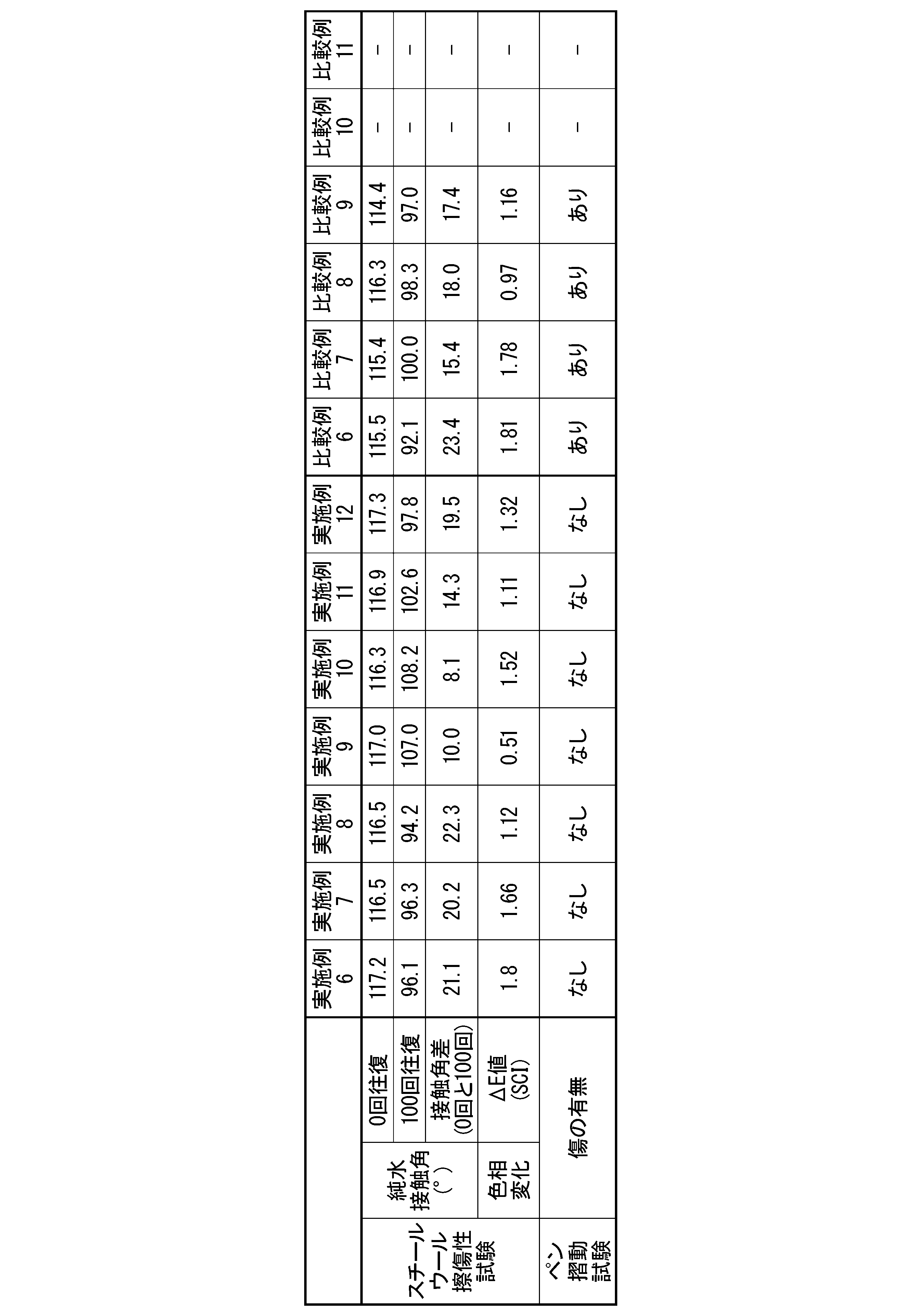
例えば、本実施形態のクリア型の光学積層体10の防汚層15は、以下の特性を有する。
(1)スチールウールを500回水平往復運動させることによる擦傷性試験後の水に対する接触角差が12°以下である。
(2)スチールウールを500回水平往復運動させることによる擦傷性試験後の水に対する接触角が109°以上である。
For example, the
(1) The difference in contact angle with water is 12° or less after the abrasion test by horizontally reciprocating steel wool 500 times.
(2) A water contact angle of 109° or more after a scratch resistance test in which steel wool is horizontally reciprocated 500 times.
(3)ウェス(不織布ワイパー)を4000回往復させることによる擦傷性試験後の水に対する接触角が100°以上である。
(4)スチールウールを500回水平往復運動させることによる擦傷性試験前後のSCI(Specular Component Include、正反射光を考慮に入れた反射色の測定方法)による下記式(3)で示されるL*a*b*値の変化量(ΔE値)が、3.0以下である。
(3) A water contact angle of 100° or more after a scratch resistance test by reciprocating a waste cloth (nonwoven fabric wiper) 4000 times.
(4) L * represented by the following formula (3) by SCI (Specular Component Include, a method of measuring reflected color in consideration of specular light) before and after a scratch resistance test by horizontally reciprocating steel wool 500 times The amount of change in a * b * value (ΔE value) is 3.0 or less.

(5)スチールウールを500回水平往復運動させることによる擦傷性試験前後のSCE(Specular Component Exclude、正反射光を考慮に入れない反射色の測定法)による下記式(4)で示されるL*a*b*値の変化量(ΔE値)が、0.5以下である。 (5) L * represented by the following formula (4) by SCE (Specular Component Exclude, a method of measuring reflected color without considering specular light) before and after a scratch resistance test by horizontally reciprocating steel wool 500 times The amount of change in a * b * value (ΔE value) is 0.5 or less.

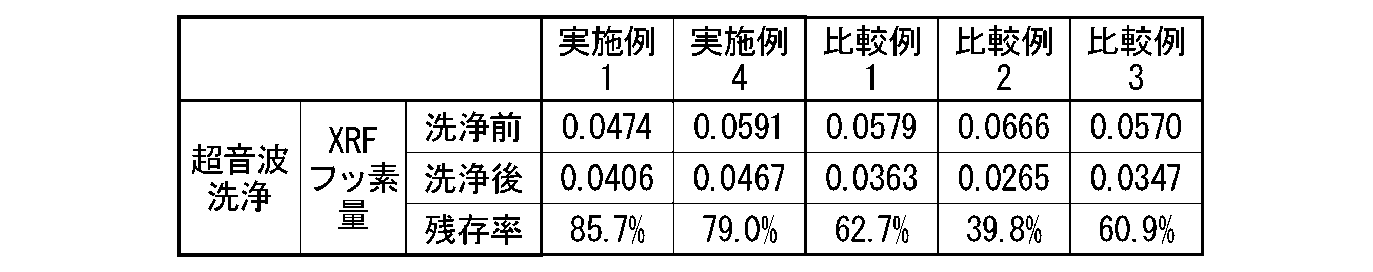
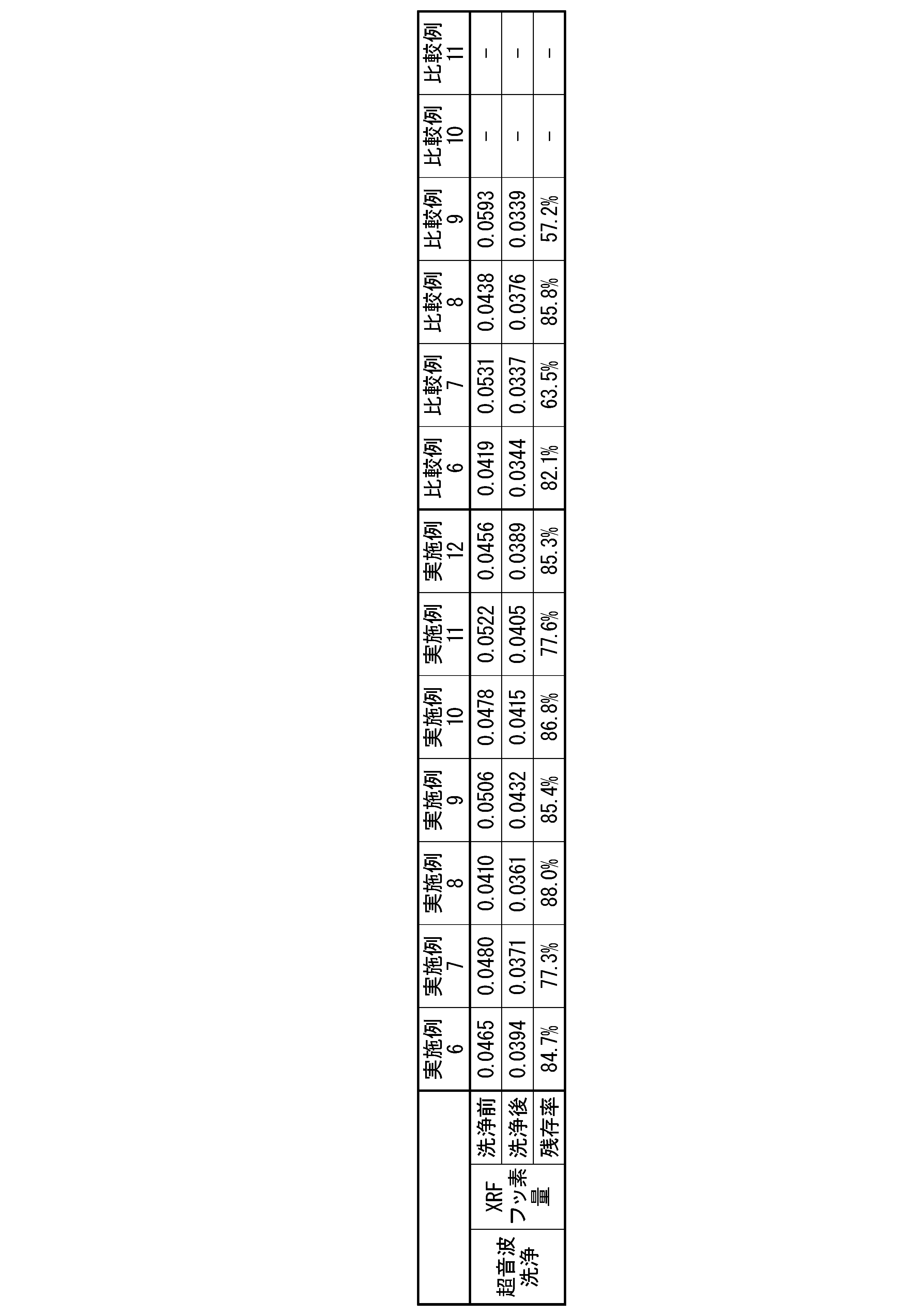
(6)濃度0.1mol/LのNaOH溶液(液温55℃)に4時間浸漬後の蛍光X線分析法(XRF)によって測定したフッ素残存率が85%以上である。 (6) The fluorine residual rate measured by X-ray fluorescence analysis (XRF) after being immersed in an NaOH solution having a concentration of 0.1 mol/L (liquid temperature of 55° C.) for 4 hours is 85% or more.
(7)ウェス(不織布ワイパー)を4000回往復させることによる擦傷性試験前後の水に対する接触角差が12°以下である。 (7) The contact angle difference to water before and after the abrasion test by reciprocating a waste cloth (non-woven fabric wiper) 4000 times is 12° or less.
(8)フッ素系溶剤中で40KHz、240Wで10分間超音波を印加した後の蛍光X線分析法(XRF)によって測定したフッ素残存率が70%以上である。 (8) The fluorine residual rate measured by X-ray fluorescence spectroscopy (XRF) after applying ultrasonic waves at 40 kHz and 240 W for 10 minutes in a fluorine-based solvent is 70% or more.
(9)水蒸気透過率が、1.5g/(m2・1day)以下である。 (9) The water vapor transmission rate is 1.5 g/(m 2 ·1 day) or less.
また例えば、本実施形態のAG型の光学積層体10の防汚層15は、以下の特性を有する。
Further, for example, the
(1)ウェス(不織布ワイパー)を4000回往復させることによる擦傷性試験前後の水に対する接触角差が7°以下である。 (1) The difference in contact angle with water before and after the abrasion test by reciprocating a waste cloth (nonwoven fabric wiper) 4000 times is 7° or less.
(2)濃度0.1mol/LのNaOH溶液(液温55℃)に4時間浸漬後の上記式(2)で示されるL*a*b*値の変化量(ΔE値)が、5.0以下である。 (2) The amount of change (ΔE value) in the L * a * b * values represented by the above formula (2) after being immersed in a NaOH solution with a concentration of 0.1 mol/L (liquid temperature: 55°C) for 4 hours is 5. 0 or less.
(3)濃度0.1mol/LのNaOH溶液(液温55℃)に4時間浸漬後の蛍光X線分析法(XRF)によって測定したフッ素残存率が90%以上である。 (3) The fluorine residual rate measured by X-ray fluorescence spectrometry (XRF) after being immersed in a NaOH solution having a concentration of 0.1 mol/L (liquid temperature of 55° C.) for 4 hours is 90% or more.
(4)フッ素系溶剤中で40KHz、240Wで10分間超音波を印加した後の蛍光X線分析法(XRF)によって測定したフッ素残存率が75%以上である。 (4) The fluorine residual rate measured by X-ray fluorescence spectroscopy (XRF) after applying ultrasonic waves at 40 KHz and 240 W for 10 minutes in a fluorine-based solvent is 75% or more.
(5)水蒸気透過率が、1.5g/(m2・1day)以下である。 (5) The water vapor transmission rate is 1.5 g/(m 2 ·1 day) or less.
蒸着によって形成した本実施形態の防汚層15を備えた光学積層体10は、塗布によって形成した防汚層と比較して、空隙が少なく緻密に形成されている。また、本実施形態の光学積層体10では、防汚層15が、防汚層15と接する低屈折率層14bに対して強固に接合している。したがって、本実施形態の光学積層体10は、可視光透過性に優れ、繰り返し摩擦に対して高い耐摩耗性を維持できるとともに、耐アルカリ性に対しても高い耐性を維持できる。
The optical
[光学積層体の製造方法]
図3に示す本実施形態の光学積層体10は、例えば、以下に示す方法により製造できる。
本実施形態では、光学積層体10の製造方法の一例として、ロール状に巻き付けられた透明基材11を用いて光学積層体10を製造する場合を例に挙げて説明する。
まず、ロール状に巻き付けられた透明基材11を巻き出す。そして、公知の方法により透明基材11上にハードコート層12となる材料を含むスラリーを塗布し、ハードコート層12となる材料に対応する公知の方法により硬化させる。このことにより、ハードコート層12を形成する(ハードコート層形成工程)。その後、表面にハードコート層12の形成された透明基材11を、公知の方法によりロール状に巻き取る。
[Method for producing an optical laminate]
The
In this embodiment, as an example of a method for manufacturing the optical
First, the
次に、ハードコート層12上に、密着層13を形成する密着層形成工程、および光学機能層14を形成する光学機能層形成工程を行う。その後、光学機能層14上に防汚層15を形成する防汚層形成工程を行う。本実施形態では、光学機能層形成工程の前に、ハードコート層12の表面を処理する第1表面処理工程を行ってから、密着層形成工程および光学機能層形成工程を行うことが好ましい。また、本実施形態では、光学機能層形成工程の後に、光学機能層14の表面を処理する第2表面処理工程を行ってから、防汚層形成工程を行うことが好ましい。
Next, an adhesion layer forming step of forming an
本実施形態の光学積層体10の製造方法において、第1表面処理工程と密着層形成工程と光学機能層形成工程と第2表面処理工程と防汚層形成工程とは、製造途中の光学積層体を減圧下の状態に維持したまま連続して行うことが好ましい。第1表面処理工程と密着層形成工程と光学機能層形成工程と第2表面処理工程と防汚層形成工程を、製造途中の光学積層体を減圧下の状態に維持したまま連続して行う場合、例えば、スパッタリング装置として特許文献4に記載された薄膜形成装置を備えた装置などを用いることができる。
In the method for manufacturing the optical
本実施形態の光学積層体の製造方法に用いることができる製造装置としては、具体的には、図4に示す製造装置20が挙げられる。
図4に示す製造装置20は、ロール巻き出し装置4と、前処理装置2Aと、スパッタリング装置1と、前処理装置2Bと、蒸着装置3と、ロール巻き取り装置5とを備えている。図4に示すように、これらの装置4、2A、1、2B、3、5は、この順に連結されている。図4に示す製造装置20は、ロールから基材を巻き出し、連結された装置(図4では、前処理装置2A、スパッタリング装置1、前処理装置2B、蒸着装置3)を連続して通過させた後に巻き取ることにより、基材上に複数層を連続的に形成するロールトゥロール方式の製造装置である。
Specifically, a
A
ロールトゥロール方式の製造装置を用いて光学積層体10を製造する場合、製造途中の光学積層体10の搬送速度(ラインスピード)は、適宜設定することができる。搬送速度は、例えば、0.5~20m/minとすることが好ましく、0.5~10m/minとすることがより好ましい。
When the optical
<ロール巻き出し装置>
図4に示すロール巻き出し装置4は、内部が所定の減圧雰囲気とされたチャンバー34と、チャンバー34内の気体を排出して減圧雰囲気とする1つまたは複数の真空ポンプ21(図4においては1つ)と、チャンバー34内に設置された巻き出しロール23およびガイドロール22を有する。図4に示すように、チャンバー34は、スパッタリング装置1のチャンバー31と前処理装置2Aを介して連結されている。
巻き出しロール23には、表面にハードコート層12の形成された透明基材11が巻き付けられている。巻き出しロール23は、所定の搬送速度で、表面にハードコート層12の形成された透明基材11を、前処理装置2Aに供給する。
<Roll unwinding device>
The
A
<前処理装置2A>
図4に示す前処理装置2Aは、内部が所定の減圧雰囲気とされたチャンバー32と、キャンロール26と、複数(図4では2つ)のガイドロール22と、プラズマ放電装置42とを有する。図4に示すように、キャンロール26と、ガイドロール22と、プラズマ放電装置42は、チャンバー32内に設置されている。図4に示すように、チャンバー32は、スパッタリング装置1のチャンバー31と連結されている。
<
A
キャンロール26およびガイドロール22は、所定の搬送速度で、ロール巻き出し装置4から送られたハードコート層12が形成された透明基材11を搬送し、ハードコート層12の表面が処理された透明基材11をスパッタリング装置1に送り出す。
プラズマ放電装置42は、図4に示すように、キャンロール26の外周面と所定の間隔で離間して対向配置されている。プラズマ放電装置42は、気体をグロー放電により電離させる。気体としては、安価かつ不活性で光学特性に影響を及ぼさないものが好ましく、例えば、アルゴンガス、酸素ガス、窒素ガス、ヘリウムガス等を使用できる。本実施形態では、気体として、アルゴンガス又は酸素ガスを用いることが好ましい。
The can roll 26 and the
As shown in FIG. 4, the
<スパッタリング装置>
図4に示すスパッタリング装置1は、内部が所定の減圧雰囲気とされたチャンバー31と、チャンバー31内の気体を排出して減圧雰囲気とする1つまたは複数の真空ポンプ21(図4においては2つ)と、成膜ロール25と、複数(図4では2つ)のガイドロール22と、複数(図4に示す例では4つ)の成膜部41とを有する。図4に示すように、成膜ロール25と、ガイドロール22と、成膜部41は、チャンバー31内に設置されている。図4に示すように、チャンバー31は、前処理装置2Bのチャンバー32と連結されている。
<Sputtering device>
The sputtering apparatus 1 shown in FIG. 4 includes a
成膜ロール25およびガイドロール22は、所定の搬送速度で、前処理装置2Aから送られた表面が処理されたハードコート層12の形成された透明基材11を搬送し、ハードコート層12上に、密着層13および光学機能層14の形成された透明基材11を前処理装置2Bに供給する。
図4に示すスパッタリング装置1では、成膜ロール25上を走行する透明基材11のハードコート層12上に、スパッタリングによって密着層13が積層され、その上に高屈折率層14aと低屈折率層14bが交互に積層されて、光学機能層14が形成される。
The film-forming
In the sputtering apparatus 1 shown in FIG. 4, the
成膜部41は、図4に示すように、成膜ロール25の外周面と所定の間隔で離間して対向配置され、成膜ロール25を囲むように複数設けられている。成膜部41の数は、密着層13と、光学機能層14を形成している高屈折率層14aと低屈折率層14bとの合計積層数に応じて決定される。密着層13および光学機能層14を形成している高屈折率層14aと低屈折率層14bの合計積層数が多いために、隣接する成膜部41間の距離を確保しにくい場合には、チャンバー31内に成膜ロール25を複数設け、各成膜ロール25の周囲に成膜部41を配置してもよい。成膜ロール25を複数設ける場合、必要に応じてさらにガイドロール22を設置してもよい。成膜ロール25と成膜部41が設けられたチャンバー31を複数台連結してもよい。また、隣接する成膜部41間の距離を確保しやすくするために、成膜ロール25の直径を適宜変更してもよい。
As shown in FIG. 4 , the
各成膜部41には、それぞれ所定のターゲット(不図示)が設置されている。ターゲットには、公知の構造により、電圧が印加されるようになっている。本実施形態では、ターゲットの近傍に、ターゲットに所定の反応性ガスおよびキャリアガスを所定の流量で供給するガス供給部(不図示)と、ターゲットの表面に磁場を形成する公知の磁場発生源(不図示)とが設けられている。
A predetermined target (not shown) is installed in each
ターゲットの材料、および反応性ガスの種類および流量は、成膜部41と成膜ロール25との間を通過することによって透明基材11上に形成される密着層13、高屈折率層14a、低屈折率層14bの組成に応じて適宜決定される。例えば、SiO2からなる層を形成する場合、ターゲットとしてSiを用い、反応性ガスとしてO2を用いる。また、例えば、Nb2O5からなる層を形成する場合、ターゲットとしてNbを用い、反応性ガスとしてO2を用いる。低屈折率層14bは、0.5Pa未満の真空度で成膜することが好ましく、高屈折率層14aは、1.0Pa未満の真空度で成膜することが好ましい。これらの層を当該真空度で成膜すると、光学機能層14が緻密になり、水蒸気透過率が低下し、耐久性等が向上する。
The material of the target and the type and flow rate of the reactive gas are determined by the
本実施形態では、成膜速度の高速化の観点から、スパッタ法として、マグネトロンスパッタ法を用いることが好ましい。
なお、スパッタ法は、マグネトロンスパッタ法に限定されるものではなく、直流グロー放電または高周波によって発生させたプラズマを利用する2極スパッタ方式、熱陰極を付加する3極スパッタ方式などを用いてもよい。
In the present embodiment, it is preferable to use magnetron sputtering as the sputtering method from the viewpoint of increasing the film formation speed.
The sputtering method is not limited to the magnetron sputtering method, and a two-electrode sputtering method using plasma generated by DC glow discharge or high frequency, a three-electrode sputtering method using a hot cathode, or the like may be used. .
スパッタリング装置1は、密着層13および光学機能層14となる各層を成膜した後に、光学特性を測定する測定部としての光学モニター(不図示)を備える。これにより、形成された密着層13および光学機能層14の品質を確認できる。スパッタリング装置1が、例えば、2つ以上のチャンバーを有する場合、各チャンバー内に光学モニターを設置することが好ましい。
The sputtering apparatus 1 includes an optical monitor (not shown) as a measurement unit for measuring optical characteristics after forming the respective layers to be the
光学モニター(不図示)としては、例えば、幅方向にスキャン可能な光学ヘッドにより、ハードコート層12上に形成された密着層13および光学機能層14の幅方向の光学特性を測定するものが挙げられる。このような光学モニターが備えられている場合、例えば、光学特性として反射率のピーク波長を測定し、光学厚みに換算することにより、密着層13および光学機能層14の幅方向の光学厚み分布を測定できる。光学モニターを用いて光学特性を測定することにより、リアルタイムでスパッタ条件を調整しながら、最適な光学特性を有する密着層13および光学機能層14を備える光学積層体10を形成できる。
An example of the optical monitor (not shown) is one that measures the optical characteristics in the width direction of the
<前処理装置2B>
図4に示す前処理装置2Bは、内部が所定の減圧雰囲気とされたチャンバー32と、キャンロール26と、複数(図4では2つ)のガイドロール22と、プラズマ放電装置42とを有する。図4に示すように、キャンロール26と、ガイドロール22と、プラズマ放電装置42は、チャンバー32内に設置されている。図4に示すように、チャンバー32は、蒸着装置3のチャンバー33と連結されている。
<
The
キャンロール26およびガイドロール22は、所定の搬送速度で、スパッタリング装置1から送られた光学機能層14までの各層が形成された透明基材11を搬送し、光学機能層14の表面が処理された透明基材11を蒸着装置3に送り出す。
プラズマ放電装置42としては、例えば、前処理装置2Aと同様のものを用いることができる。
The can roll 26 and the
As the
<蒸着装置>
図4に示す蒸着装置3は、内部が所定の減圧雰囲気とされたチャンバー33と、チャンバー33内の気体を排出して減圧雰囲気とする1つまたは複数の真空ポンプ21(図4においては1つ)と、複数(図4では4つ)のガイドロール22と、蒸着源43と、加熱装置53とを有する。図4に示すように、ガイドロール22と、蒸着源43は、チャンバー33内に設置されている。チャンバー33は、ロール巻き取り装置5のチャンバー35と連結されている。
<Evaporation equipment>
The
蒸着源43は、隣接する2つのガイドロール22間を略水平に搬送されている、光学機能層14の表面が処理された透明基材11と、対向して配置されている。蒸着源43は、防汚層15となる材料からなる蒸発ガスを、光学機能層14上に供給する。蒸着源43の向きは、任意に設定できる。
加熱装置53は、防汚層15となる材料を蒸気圧温度に加熱する。加熱装置53としては、抵抗加熱方式、ヒーター加熱方式、誘導加熱方式、電子ビーム方式で加熱するものなどを用いることができる。抵抗加熱方式では、防汚層15となる防汚性材料を収容する容器を抵抗体として通電加熱する。ヒーター加熱方式では、容器の外周に配置したヒーターで容器を加熱する。誘導加熱方式では、外部に設置した誘導コイルから電磁誘導作用によって容器又は防汚性材料を加熱する。
The
The
図4に示す蒸着装置3は、蒸着源43で蒸発させた蒸着材料を所定の位置に導く案内板(不図示)と、蒸着により形成された防汚層15の厚みを観察する膜厚計(不図示)と、チャンバー33内の圧力を測定する真空圧計(不図示)と、電源装置(不図示)とを備えている。
案内板は、蒸発させた蒸着材料を、所望の位置に導くことができれば如何なる形状であってもよい。案内板は、必要でなければ備えなくとも差し支えない。
真空圧計としては、例えば、イオンゲージなどを用いることができる。
電源装置としては、例えば、高周波電源などが挙げられる。
The
The guide plate may have any shape as long as it can guide the evaporated vapor deposition material to a desired position. If the guide plate is not necessary, it does not matter if it is not provided.
For example, an ion gauge or the like can be used as the vacuum pressure gauge.
Examples of the power supply include a high frequency power supply.
<ロール巻き取り装置>
図4に示すロール巻き取り装置5は、内部が所定の減圧雰囲気とされたチャンバー35と、チャンバー35内の気体を排出して減圧雰囲気とする1つまたは複数の真空ポンプ21(図4においては1つ)と、チャンバー35内に設置された巻き取りロール24およびガイドロール22とを有する。
巻き取りロール24には、表面に防汚層15までの各層の形成された透明基材11(光学積層体10)が巻き付けられている。巻き取りロール24およびガイドロール22は、所定の巻き取り速度で、光学積層体10を巻き取る。
必要に応じ、キャリアフィルムも用いても良い。
<Roll take-up device>
The roll winding device 5 shown in FIG. 4 includes a
The take-
A carrier film may also be used as necessary.
図4に示す製造装置20に備えられている真空ポンプ21としては、例えば、ドライポンプ、油回転ポンプ、ターボ分子ポンプ、油拡散ポンプ、クライオポンプ、スパッタイオンポンプ、ゲッターポンプなどを用いることができる。真空ポンプ21は、各チャンバー31、32、33、34、35において、所望の減圧状態を作り出すために適宜選択し、あるいは組み合わせて用いることができる。
As the
真空ポンプ21は、スパッタリング装置1のチャンバー31と蒸着装置3のチャンバー33の双方を所望の減圧状態に維持できればよく、製造装置20における真空ポンプ21の設置位置および数は特に限定されない。また、図4に示す製造装置20では、ロール巻き出し装置4と前処理装置2Aとスパッタリング装置1と前処理装置2Bと蒸着装置3とロール巻き取り装置5とが、連結されている。このため、真空ポンプ21は、チャンバー31、32、33、34、35にそれぞれ設置されていてもよいし、スパッタリング装置1のチャンバー31と蒸着装置3のチャンバー33の双方を所望の減圧状態に維持できるのであれば、チャンバー31、32、33、34、35のうち、一部のチャンバーにのみ設置されていてもよい。
The
次に、図4に示す製造装置20を用いて、第1表面処理工程と密着層形成工程および光学機能層形成工程と第2表面処理工程と防汚層形成工程を、製造途中の光学積層体10を減圧下の状態に維持したまま連続して行う方法について、説明する。
まず、ロール巻き出し装置4のチャンバー34内に、表面にハードコート層12の形成された透明基材11が巻き付けられた巻き出しロール23を設置する。そして、巻き出しロール23およびガイドロール22を回転させて、所定の搬送速度で、表面にハードコート層12の形成された透明基材11を、前処理装置2Aに送り出す。
Next, using the
First, in the
次に、前処理装置2Aのチャンバー32内で、密着層13および光学機能層14の形成される表面に対する前処理として、第1表面処理工程を行う。本実施形態では、ハードコート層12の形成された透明基材11に対して第1表面処理工程を行う。
第1表面処理工程では、キャンロール26およびガイドロール22を回転させて、所定の搬送速度で、ハードコート層12の形成された透明基材11を搬送しながら、キャンロール26上を走行するハードコート層12の表面を処理する。
Next, in the
In the first surface treatment step, the can roll 26 and the
ハードコート層12の表面処理方法としては、例えば、グロー放電処理、プラズマ処理、イオンエッチング、アルカリ処理などを用いることができる。これらの中でも、大面積処理が可能であるため、グロー放電処理を用いることが好ましい。グロー放電処理は、例えば、0.1~10kwhの処理強度で行うことができる。
ハードコート層12の表面に対して、グロー放電処理を行うことにより、ハードコート層12の表面がナノレベルで粗面化されるとともに、ハードコート層12の表面に存在する結合力の弱い物質が除去される。その結果、ハードコート層12と、ハードコート層12上に形成される光学機能層14との密着性が良好となる。
As a surface treatment method for the
By performing a glow discharge treatment on the surface of the
次に、スパッタリング装置1のチャンバー31内で、密着層形成工程および光学機能層形成工程を行う。具体的には、成膜ロール25およびガイドロール22を回転させて、所定の搬送速度で、ハードコート層12の形成された透明基材11を搬送しながら、成膜ロール25上を走行するハードコート層12上に、密着層13および光学機能層14を形成する。
Next, an adhesion layer forming step and an optical function layer forming step are performed in the
本実施形態では、各成膜部41に設置するターゲットの材料、またはガス供給部から供給する反応性ガスの種類および流量を変化させてスパッタリングすることによって、密着層13を形成し、その上に高屈折率層14aと低屈折率層14bとを交互に積層する。すなわち、密着層形成工程と光学機能層形成工程は、スパッタリング装置1内で連続して行われる。このことにより、密着層13と反射防止層である光学機能層14とを形成する。高屈折率層14aと低屈折率層14bとは、それぞれ所定の真空度以下の条件で成膜する。具体的には、高屈折率層14aを1.0Pa未満の真空度で成膜し、低屈折率層14bを0.5Pa未満の真空度で成膜する。
In the present embodiment, the
密着層13としてSiOx膜を成膜する場合、シリコンターゲットを用いて、酸素ガスとアルゴンガスの混合ガス雰囲気による反応性スパッタリングにより形成することが好ましい。
密着層13と高屈折率層14aと低屈折率層14bとをスパッタリングによって連続して積層する場合、密着層13の成膜時と高屈折率層14aの成膜時と低屈折率層14bの成膜時とでターゲットの材料を変えて成膜してもよい。また、例えば、1種類の材料をターゲットとして用い、スパッタリング時の酸素(反応性ガス)流量を変えることによって、ターゲット材料からなる層とターゲット材料の酸化物からなる層とを交互に形成し、密着層13と高屈折率層14aと低屈折率層14bとしても良い。
When a SiOx film is formed as the
When the
密着層13および光学機能層14を形成するためのスパッタリング時の圧力は、スパッタする金属により異なるが、2Pa以下であってもよく、1Pa以下であることが好ましく、0.6Pa以下であることがより好ましく、0.2Pa以下であることが特に好ましい。スパッタリング時の圧力が1Pa以下の減圧下の状態であると、成膜分子の平均自由工程が長くなり、成膜分子のエネルギーが高いまま積層されるため、緻密でより良好な膜質となる。高屈折率層と低屈折率層のスパッタリング時の圧力は、異なっているほうが好ましい。成膜種ごとに平均自由工程が異なるためである。成膜種ごとに圧力を変えることで、より緻密な膜を成膜することができる。
The pressure during sputtering for forming the
その後、ハードコート層12上に密着層13および光学機能層14の形成された透明基材11を、成膜ロール25およびガイドロール22の回転によって、前処理装置2Bに送り出す。
次に、前処理装置2Bのチャンバー32内で、防汚層15の形成される表面に対する前処理として、第2表面処理工程を行う。本実施形態では、光学機能層形成工程によって得られた光学機能層14の形成された透明基材11を、大気に触れさせることなく、減圧下の状態に維持したまま連続して第2表面処理工程を行う。
第2表面処理工程では、キャンロール26およびガイドロール22を回転させて、所定の搬送速度で、光学機能層14までの各層が形成された透明基材11を搬送しながら、キャンロール26上を走行する光学機能層14の表面に、放電処理を行う。
After that, the
Next, in the
In the second surface treatment step, the can roll 26 and the
光学機能層14の表面処理方法としては、例えば、グロー放電処理、プラズマ処理、イオンエッチング、アルカリ処理などを用いることができる。これらの中でも、大面積処理が可能であるため、グロー放電処理を用いることが好ましい。
As a surface treatment method for the
光学機能層14の表面に放電処理を行うと、光学機能層14の表面がエッチングされ、光学機能層14の表面状態が変化する。光学機能層14の表面状態は、表面粗さRa又は要素の平均長さRSmで表される。例えば、光学機能層14のヘイズが2.0以下のクリア型の反射防止フィルムの場合は、光学機能層14の表面状態は表面粗さRaで定義しやすい。また例えば、光学機能層14のヘイズが2.0超のAG型の反射防止フィルムの場合は、光学機能層14の表面状態は要素の平均長さRSmで定義しやすい。表面粗さRa及び要素の平均長さRSmは、JIS B0601(ISO4287)に準拠して測定される。
When the surface of the
グロー放電処理の際の積算出力は、130W・min/m2以上2000W・min/m2以下であることが好ましい。グロー放電処理の積算出力によって、光学機能層14の表面状態が変化する。本実施形態において、積算出力とは、放電処理の際に、光学機能層14に照射されたグロー放電出力と照射時間の積を、単位面積当たりで除した値である。
The integrated output during glow discharge treatment is preferably 130 W·min/m 2 or more and 2000 W·min/m 2 or less. The surface state of the
放電処理の条件は、適宜設定できる。放電処理の条件を適切に設定することで、光学機能層14と、その上に形成される防汚層15との密着性が良好となり、より一層耐摩擦性および耐アルカリ性の良好な光学積層体10が得られる。
放電処理後の光学機能層14の表面粗さRa及び要素の平均長さRSmは、光学機能層14の下に設けられているハードコート層12の表面粗さ及び要素の平均長さRSmによって異なる。
また、放電処理後の光学機能層14の表面粗さRa及び要素の平均長さRSmは、光学機能層14の上に形成される防汚層15の表面粗さRa及び要素の平均長さRSmに影響する。
Conditions for the discharge treatment can be set as appropriate. By appropriately setting the conditions of the discharge treatment, the adhesion between the
The surface roughness Ra and the average element length RSm of the
Further, the surface roughness Ra and the average length RSm of the elements of the
第2表面処理工程では例えば、下記(式1)で表される表面粗さの変化率が1~25%となるように、光学機能層の表面を処理する。特にクリア型の反射防止フィルムの場合にこの条件で光学機能層の表面を処理する。
表面粗さの変化率(%)=((Ra2/Ra1)-1)×100(%)・・・式(1)(式(1)中、Ra1は表面を処理する前の光学機能層の表面粗さ(Ra)を示し、Ra2は表面を処理した後の光学機能層の表面粗さ(Ra)を示す。)
In the second surface treatment step, for example, the surface of the optical function layer is treated so that the rate of change in surface roughness represented by the following (Equation 1) is 1 to 25%. Especially in the case of a clear type antireflection film, the surface of the optical function layer is treated under these conditions.
Change rate of surface roughness (%)=((Ra2/Ra1)-1)×100(%) Formula (1) (wherein Ra1 is the optical function layer before surface treatment) indicates the surface roughness (Ra), and Ra2 indicates the surface roughness (Ra) of the optical function layer after surface treatment.)
第2表面処理工程は、(式1)で表される表面粗さの変化率が、1%~25%となるように行うことが好ましく、10%~20%となるように行うことがより好ましい。(式1)で表される表面粗さの変化率が1%以上であると、第2表面処理工程を行うことによる光学機能層14と防汚層15との密着性向上効果が顕著となる。また、(式1)で表される表面粗さの変化率が、25%以下であると、光学機能層14の厚みが適切であるため、光学機能層14上に厚みの均一な防汚層15が形成される。
The second surface treatment step is preferably performed so that the surface roughness change rate represented by (Formula 1) is 1% to 25%, more preferably 10% to 20%. preferable. When the change rate of the surface roughness represented by (Formula 1) is 1% or more, the effect of improving the adhesion between the
また第2表面処理工程では、下記式で表される要素の平均長さの変化率が7~65%となるように、光学機能層の表面を処理する。特にAG型の反射防止フィルムの場合にこの条件で光学機能層の表面を処理する。例えば、放電処理の際の積算出力は、要素の平均長さに影響を及ぼすパラメータの一つである。
要素の平均長さの変化率(%)=((RSm2/RSm1)-1)×100(%)…式(2)
(式(2)中、RSm1は表面を処理する前の光学機能層の要素の平均長さ(RSm)を示し、RSm2は表面を処理した後の光学機能層の要素の平均長さ(RSm)を示す。)
In the second surface treatment step, the surface of the optical function layer is treated so that the average length change rate of the elements represented by the following formula is 7 to 65%. Especially in the case of an AG type antireflection film, the surface of the optical function layer is treated under these conditions. For example, the integrated output during discharge treatment is one of the parameters that affects the average length of the element.
Rate of change in average length of elements (%) = ((RSm2/RSm1)-1) x 100 (%) Equation (2)
(In formula (2), RSm1 indicates the average length (RSm) of the elements of the optical function layer before surface treatment, and RSm2 indicates the average length (RSm) of the elements of the optical function layer after surface treatment. indicates.)
本実施形態において、光学機能層14の表面粗さRa及び要素の平均長さは、原子間力顕微鏡(AFM:Atomic Force Microscope)を用いて、測定できる。表面粗さRaは、光学機能層14の表面の面積1μm2の範囲で測定し、要素の平均長さRSmは、光学機能層14の表面の面積0.5μm2の範囲で測定する。
In this embodiment, the surface roughness Ra of the
その後、光学機能層14の表面が処理された透明基材11を、キャンロール26およびガイドロール22の回転によって、蒸着装置3に送り出す。
次に、蒸着装置3のチャンバー33内で、防汚層形成工程を行う。本実施形態では、第2表面処理工程によって得られた光学機能層14の表面が処理された透明基材11を、大気に触れさせることなく、減圧下の状態に維持したまま連続して防汚層形成工程を行う。 防汚層形成工程では、ガイドロール22を回転させて、所定の搬送速度で、光学機能層14の表面が処理された透明基材11を搬送しながら、光学機能層14の表面に蒸着源43を蒸着する。
Thereafter, the
Next, an antifouling layer forming step is performed in the
本実施形態では、例えば、防汚層15となるフッ素系有機化合物からなる防汚性材料を、加熱装置53によって蒸気圧温度に加熱し、得られた蒸発ガスを減圧環境下において蒸着源43から供給し、表面が処理された光学機能層14に付着させ、防汚層15を真空蒸着によって形成する。
防汚層15の真空蒸着を行う際の圧力は、例えば、0.05Pa以下であることが好ましく、0.01Pa以下であることがより好ましく、0.001Pa以下であることが特に好ましい。真空蒸着を行う際の圧力が、0.05Pa以下の減圧下の状態であると、成膜分子の平均自由工程が長く、蒸着エネルギーが高くなるため、緻密でより良好な防汚層15が得られる。
In the present embodiment, for example, an antifouling material made of a fluorine-based organic compound that serves as the
The pressure at which the
以上の方法により、スパッタリングによって形成された密着層13および光学機能層14上に、真空蒸着によって防汚層15が形成された光学積層体10が得られる。成膜後の防汚層15は、蛍光X線分析法(XRF)を用いて測定したフッ素の初期量が0.03以上であることが好ましい。
By the above method, the
その後、防汚層15までの各層が形成された透明基材11(光学積層体10)を、ガイドロール22の回転によって、ロール巻き取り装置5に送り出す。
そして、ロール巻き取り装置5のチャンバー35内で、巻き取りロール24およびガイドロール22の回転によって、光学積層体10を巻き取りロール24に巻き付ける。
After that, the transparent substrate 11 (optical layered body 10 ) on which the layers up to the
Then, the
本実施形態では、光学機能層形成工程と防汚層形成工程とを、減圧下で連続して行うことが好ましい。特に、図4に示す製造装置20を用いる本実施形態の製造方法のように、光学積層体10をロールトゥロール方式で巻重体として連続的に製造する場合には、光学機能層形成工程と防汚層形成工程とを、減圧状態を維持したままインラインで連続して行うことがより好ましい。インラインとは、光学機能層形成工程において形成した光学機能層14を大気に触れさせることなく、防汚層形成工程を行うことを意味する。光学機能層形成工程と防汚層形成工程とを減圧下で連続して行うことにより、防汚層15を形成する前に、光学機能層形成工程において形成した光学機能層14上に、自然酸化膜が生成されることが抑制される。また、ロールを巻き取る際の異物などのコンタミネーションが、光学機能層14上に付着して、光学機能層14と防汚層15との密着性を阻害することを防止できる。したがって、光学機能層形成工程後、光学機能層14までの各層の形成された透明基材11を減圧状態のチャンバーから取り出し、その後、再びチャンバー内に設置して減圧下で防汚層形成工程を行う場合(後述する実施例4の場合)と比較して、光学機能層14と防汚層15との密着性が良好で、透明性に優れる光学積層体が得られる。
In this embodiment, it is preferable to continuously perform the optical function layer forming step and the antifouling layer forming step under reduced pressure. In particular, as in the manufacturing method of the present embodiment using the
また、本実施形態の光学積層体10の有する防汚層15は、蒸着膜であるため、例えば、塗布法により形成した防汚膜と比較して、高い耐摩耗性が得られる。これは、以下に示す理由によるものと推定される。すなわち、塗布法により形成した防汚膜中には、塗料に含まれている溶剤に起因する空隙が存在している。これに対し、蒸着膜には、溶剤に起因する空隙が存在しない。このため、蒸着膜は、塗布法により形成した防汚膜と比較して、高密度であり、高い耐摩耗性や耐アルカリ性が得られるものと推定される。
Further, since the
本実施形態の光学積層体10の製造方法は、密着層13を形成する密着層形成工程と、高屈折率層14aと低屈折率層14bとを交互に積層することにより光学機能層14を形成する光学機能層形成工程と、光学機能層14の表面を処理する第2表面処理工程と、表面処理された光学機能層14上に防汚層15を形成する防汚層形成工程とを含む。このため、光学機能層14と、光学機能層14上に形成された防汚層15との密着性が良好であり、より一層摩擦性および耐アルカリ性の良好なものとなる。
The method for manufacturing the optical
特に、第2表面処理工程において、式(1)で表される表面粗さの変化率が1~25%となるように、光学機能層の表面を処理した場合、光学機能層14の表面が適切な粗さに変化し、かつ、エッチングされることにより表面が活性化されるため、光学機能層14上に形成される防汚層15との反応性が向上するため好ましい。
また、本実施形態の光学積層体10の製造方法では、ロールトゥロール方式で光学積層体10を連続して形成でき、かつ、高精度で膜厚をコントロールできるため、光学機能層形成工程において、スパッタリングによって光学機能層14を形成することが好ましい。
In particular, in the second surface treatment step, when the surface of the optical functional layer is treated so that the surface roughness change rate represented by formula (1) is 1 to 25%, the surface of the optical
In addition, in the method for manufacturing the optical
本実施形態において、第1表面処理工程と光学機能層形成工程と第2表面処理工程と防汚層形成工程を、製造途中の光学積層体を減圧下の状態に維持したまま連続して行う場合、各製造工程に支障のない範囲であれば、例えば、スパッタリング装置と蒸着装置とで、チャンバー内の減圧条件が異なっていても構わない。 In the present embodiment, when the first surface treatment step, the optical function layer forming step, the second surface treatment step, and the antifouling layer forming step are continuously performed while the optical layered body during production is maintained under reduced pressure. For example, the pressure reduction conditions in the chamber may be different between the sputtering apparatus and the vapor deposition apparatus, as long as they do not interfere with each manufacturing process.
本実施形態においては、密着層形成工程、光学機能層形成工程、防汚層形成工程のいずれか1つ以上の工程において、経時的に成膜結果を測定器により測定し、その結果を後工程にあたる製造工程の条件にフィードバックすることが好ましい。このことにより、光学積層体全体の特性を最適化しやすくなり、光学積層体の面内での特性を均一にできる。また、測定器により同一工程における製造条件のフィードバックを行うこともできる。この場合、その工程で成膜された層が、均一で安定した特性を有するものとなる。 In the present embodiment, in one or more steps of the adhesion layer forming step, the optical function layer forming step, and the antifouling layer forming step, the film formation results are measured with a measuring instrument over time, and the results are used in the post-process. It is preferable to feed back to the conditions of the manufacturing process corresponding to This makes it easier to optimize the properties of the entire optical layered body, and makes it possible to make the properties of the optical layered body uniform within the plane. In addition, it is also possible to feed back manufacturing conditions in the same process using a measuring instrument. In this case, the layer formed in that process has uniform and stable characteristics.
本実施形態においては、光学機能層形成工程と防汚層形成工程との間に第2表面処理工程を行う場合を例に挙げて説明したが、第2表面処理工程は必要に応じて行えばよく、行わなくてもよい。第2表面処理工程を行わない場合においても、光学機能層形成工程と防汚層形成工程とを、減圧下で連続して行うことが好ましい。 In the present embodiment, the case where the second surface treatment step is performed between the optical function layer forming step and the antifouling layer forming step has been described as an example. Well, you don't have to. Even when the second surface treatment step is not performed, it is preferable to continuously perform the optical functional layer forming step and the antifouling layer forming step under reduced pressure.
また本実施形態における製造方法では、光学機能層を所定の真空度以下の条件で成膜する。そのため、光学機能層14が緻密になり、水蒸気透過率が低下し、耐摩擦性及び耐アルカリ性が向上する。さらに、防汚層の膜厚が所定の厚み以上であることで、十分な耐擦傷性及び耐アルカリ性を確保できる。
In addition, in the manufacturing method according to the present embodiment, the optical function layer is formed under conditions of a predetermined degree of vacuum or less. Therefore, the
本実施形態においては、前処理装置2Aと、スパッタリング装置1と、前処理装置2Bと、蒸着装置3と、ロール巻き出し装置4と、ロール巻き取り装置5とを備えている図4に示す製造装置20を用いて、ロールトゥロール方式で光学積層体10を連続的に製造する場合を例に挙げて説明したが、光学積層体10を製造する製造装置は、図4に示す製造装置20に限定されない。
例えば、前処理装置2Aおよび前処理装置2Bを含まず、ロール巻き出し装置4と、スパッタリング装置1と、蒸着装置3と、ロール巻き取り装置5とが、この順に連結された製造装置を用いてもよい。
In this embodiment, the manufacturing process shown in FIG. The case where the optical
For example, using a manufacturing apparatus in which the
図4に示す製造装置20には、蒸着装置3のチャンバー33と前処理装置2Bのチャンバー32との間に、防汚層15の形成される光学機能層14の表面を洗浄するための前処理室(不図示)が設けられていてもよい。
図4に示す製造装置20には、蒸着装置3のチャンバー33とロール巻き取り装置5のチャンバー35との間に、防汚層15までの各層が形成された透明基材11の冷却および/または検査を行うための後処理室(不図示)が設けられていてもよい。
In the
The
図4に示す製造装置20には、ロール巻き出し装置4とスパッタリング装置1との間に、透明基材11の表面にハードコート層12を形成するためのハードコート層形成装置が設けられていてもよい。この場合、光学機能層14と防汚層15だけでなく、ハードコート層12も、ロールトゥロール方式で連続的に製造でき、好ましい。
A
本実施形態においては、スパッタリング装置を用いて光学機能層形成工程を行い、蒸着装置を用いて防汚層形成工程を行う場合を例に挙げて説明したが、第2表面処理工程を行わない場合には、光学機能層形成工程と防汚層形成工程とを同じ装置(1つのチャンバー内)で行ってもよい。 In the present embodiment, the case where the optical function layer forming step is performed using a sputtering device and the antifouling layer forming step is performed using a vapor deposition device has been described as an example, but the case where the second surface treatment step is not performed. Alternatively, the optical functional layer forming step and the antifouling layer forming step may be performed in the same apparatus (in one chamber).
本実施形態の光学積層体10に於いて、透明基材の光学機能層などが形成された面と対向する面に、必要に応じて各種の層を設けてもよい。例えば、他の部材との接着に用いられる粘着剤層が設けられていても良い。また、この粘着剤層を介して他の光学フィルムが設けられていても良い。他の光学フィルムとしては、例えば偏光フィルム、位相差補償フィルム、1/2波長板、1/4波長板として機能するフィルムなどが挙げられる。
In the optical
また、透明基材の対向する面に、反射防止、選択反射、防眩、偏光、位相差補償、視野角補償又は拡大、導光、拡散、輝度向上、色相調整、導電などの機能を有する層が直接形成されていても良い。
また、光学積層体の形状は、平滑な形状であってもよいし、モスアイ、防眩機能を発現するナノオーダーの凹凸構造を有する形状でもよい。また、レンズ、プリズムなどのマイクロからミリオーダーの幾何学形状であっても良い。形状は、例えば、フォトリソグラフィーとエッチングの組み合わせ、形状転写、熱プレス等によって形成できる。本実施形態においては、蒸着等により成膜するため、基材に例えば凹凸形状がある場合でも、その凹凸形状を維持できる。
In addition, a layer having functions such as antireflection, selective reflection, antiglare, polarization, phase difference compensation, viewing angle compensation or enlargement, light guide, diffusion, luminance improvement, hue adjustment, and conductivity is provided on the opposite surface of the transparent base material. may be formed directly.
Further, the shape of the optical layered body may be a smooth shape or a shape having a nano-order concave-convex structure that exhibits moth-eye and anti-glare functions. Also, it may be a geometric shape of micro to millimeter order such as a lens or a prism. The shape can be formed by, for example, a combination of photolithography and etching, shape transfer, heat pressing, and the like. In this embodiment, since the film is formed by vapor deposition or the like, even if the substrate has an uneven shape, the uneven shape can be maintained.
本実施形態の物品は、例えば液晶表示パネル、有機EL表示パネルなど、画像表示部の表示面に上述した光学積層体10を設けたものである。これにより、例えば、スマートホンや操作機器のタッチパネル表示部に対して、高い耐摩耗性および耐アルカリ性を付与することができ、耐久性に優れた、実使用に好適な画像表示装置を実現できる。
The article of the present embodiment is, for example, a liquid crystal display panel, an organic EL display panel, or the like, in which the above-described optical
また、物品としては画像表示装置に限定されず、例えば本実施形態の光学積層体が表面に設けられた窓ガラスやゴーグル、太陽電池の受光面、スマートホンの画面やパーソナルコンピューターのディスプレイ、情報入力端末、タブレット端末、AR(拡張現実)デバイス、VR(仮想現実)デバイス、電光表示板、ガラステーブル表面、遊技機、航空機や電車などの運行支援装置、ナビゲーションシステム、計器盤、光学センサーの表面など光学積層体10が適用可能なものであれば、どのようなものでもよい。
In addition, the article is not limited to an image display device, and for example, a window glass or goggles having the optical laminate of the present embodiment provided on the surface, a light-receiving surface of a solar cell, a screen of a smartphone or a display of a personal computer, and an information input device. Terminals, tablet terminals, AR (augmented reality) devices, VR (virtual reality) devices, electronic display panels, glass table surfaces, game machines, operation support devices for aircraft and trains, navigation systems, dashboards, surfaces of optical sensors, etc. Any material to which the optical
以上、本発明の実施形態を説明したが、この実施形態は、例として提示したものであり、発明の範囲を限定することは意図していない。この実施形態は、その他の様々な形態で実施されることが可能であり、発明の要旨を逸脱しない範囲で、種々の省略、置き換え、変更を行うことができる。これら実施形態やその変形は、発明の範囲や要旨に含まれると同様に、特許請求の範囲に記載された発明とその均等の範囲に含まれるものである。
例えば、ハードコート層12に代えて、アンチグレア層を形成したり、柔軟性を有するソフトコート層など、必要に応じて任意の機能層を付加したりすることができる。これらは積層されていても良い。
Although the embodiment of the present invention has been described above, this embodiment is presented as an example and is not intended to limit the scope of the invention. This embodiment can be implemented in various other forms, and various omissions, replacements, and modifications can be made without departing from the scope of the invention. These embodiments and their modifications are included in the scope and spirit of the invention, as well as the scope of the invention described in the claims and equivalents thereof.
For example, instead of the
本発明の効果を検証した。
尚、以下の実施例および比較例で作成される光学積層体は、反射防止フィルムとして機能する一例であり、本発明の趣旨はこれらに限定されるものではない。
The effects of the present invention have been verified.
It should be noted that the optical laminates produced in the following examples and comparative examples are examples that function as antireflection films, and the gist of the present invention is not limited to these.
(実施例1)
まず、平均粒径50nmのシリカ粒子(フィラー)の含有量が樹脂組成物(バインダー樹脂)の固形分全体に対し、28質量%である光硬化性の樹脂組成物を準備した。樹脂組成物は、表1に示すように、シリカ粒子、アクリレート、レベリング剤、及び光重合開始剤を溶剤に溶解させて調製した。
(Example 1)
First, a photocurable resin composition was prepared in which the content of silica particles (filler) with an average particle size of 50 nm was 28% by mass with respect to the total solid content of the resin composition (binder resin). A resin composition, as shown in Table 1, was prepared by dissolving silica particles, an acrylate, a leveling agent, and a photopolymerization initiator in a solvent.

SR610:ポリエチレングリコールジアクリレート、ポリエチレングリコール鎖の平均分子量600
CN968:ポリエステル骨格を有する6官能脂肪族ウレタンアクリレート
Irgacure184:1-ヒドロキシ-シクロヘキシル-フェニル-ケトン
SR610: polyethylene glycol diacrylate, polyethylene glycol chain average molecular weight 600
CN968: 6-functional aliphatic urethane acrylate having a polyester skeleton Irgacure184: 1-hydroxy-cyclohexyl-phenyl-ketone
<ハードコート層形成工程>
透明基材11として厚さ80μm、長さ3900mのロール状のTACフィルムを用意し、TACフィルム上に表1に示す光硬化性の樹脂組成物をグラビアコーターによって塗布し、光を照射して硬化させ、厚み5μmのハードコート層12を形成した。
<Hard coat layer forming step>
A roll-shaped TAC film having a thickness of 80 μm and a length of 3900 m was prepared as the
次に、ロールトゥロール方式で、以下に示す方法により、ハードコート層12の形成された透明基材11上に、密着層13と光学機能層14と防汚層15とをこの順で連続的に製造し、実施例1の光学積層体(反射防止フィルム)を作成した。
製造装置としては、図4に示す製造装置20を用いた。また、ラインスピードは2m/minとした。第1表面処理工程と密着層形成工程と光学機能層形成工程と第2表面処理工程と防汚層形成工程を、製造途中の光学積層体を減圧下の状態に維持したまま連続して行った。
Next, by a roll-to-roll method, the
As a manufacturing apparatus, the
<第1表面処理工程>
次に、ハードコート層12に対して、グロー放電処理の処理強度を4000W・min/m2にして、グロー放電処理を行った。
<First surface treatment step>
Next, the
<密着層形成工程および光学機能層形成工程>
密着層形成工程では、SiOx層を密着層13として、圧力0.5Pa未満の条件で、成膜した。成膜は、Siターゲットを用いて、チャンバー内に酸素を導入して行った。酸素量は、プラズマ発光モニタリングで制御した。Si元素が酸化されながら成膜されることで、SiOxからなる密着層を形成した。密着層の厚みは5nmとした。次いで、高屈折率層と低屈折率層を交互に2層ずつ成膜した。高屈折率層は、Nbターゲットを用いて、チャンバー内に酸素を導入して行った。チャンバー内の圧力は、1.0Pa以下とした。Nb元素が酸化されながら成膜されることで、Nb2O5からなる高屈折率層を形成した。低屈折率層は、密着層と同様に、Siターゲットを用いて、チャンバー内に酸素を導入して行った。チャンバー内の圧力は、0.5Pa未満とした。Si元素が酸化されながら成膜されることで、SiO2からなる低屈折率層を形成した。
<Adhesion Layer Forming Step and Optical Function Layer Forming Step>
In the adhesion layer forming step, the SiO x layer was formed as the
<第2表面処理工程>
光学機能層14の表面にグロー放電処理を行った。グロー放電処理の積算出力は326W・min/m2であった。
<Second surface treatment step>
A glow discharge treatment was performed on the surface of the
<防汚層形成工程>
次に、光学機能層14上に、蒸着チャンバー内圧力0.01Pa以下、蒸着温度230℃、ラインスピード2.0m/min、フッ素を有する有機化合物であるパーフルオロポリエーテル基を有するアルコキシシラン化合物(KY-1901、信越化学工業株式会社製)からなる防汚層15を蒸着によって形成した。得られた防汚層15の光学膜厚を表2に示す。
その後、ロール状に巻き取り、実施例1の光学積層体(反射防止フィルム)を得た。
<Anti-fouling layer forming step>
Next, on the
Then, it was wound into a roll to obtain an optical laminate (antireflection film) of Example 1.

(実施例2)
防汚層15の光学膜厚が4nmとなるようにしたこと以外は、実施例1と同様にして、実施例2の光学積層体(反射防止フィルム)を得た。
(実施例3)
防汚層15の光学膜厚が3nmとなるようにしたこと以外は、実施例1と同様にして、実施例3の光学積層体(反射防止フィルム)を得た。
(Example 2)
An optical laminate (antireflection film) of Example 2 was obtained in the same manner as in Example 1, except that the optical film thickness of the
(Example 3)
An optical laminate (antireflection film) of Example 3 was obtained in the same manner as in Example 1, except that the optical film thickness of the
(実施例4)
実施例1と同様にして光学機能層形成工程まで行った後、ハードコート層12と密着層13と光学機能層14の形成されたTACフィルムを巻き取って製造装置から取り出し、大気中で、30日間、温度25℃、湿度55%の環境下で静置した。その後、ハードコート層12と密着層13と光学機能層14の形成されたTACフィルムを製造装置に設置して巻き出し、実施例1同様にして、第2表面処理工程および防汚層形成工程を行うことにより、光学機能層14上に防汚層15を形成し、ロール状に巻き取った。以上の工程により、実施例4の光学積層体(反射防止フィルム)を作製した。
実施例4の光学積層体の防汚層15の光学膜厚を表2に示す。
(Example 4)
After performing up to the optical functional layer forming step in the same manner as in Example 1, the TAC film having the
Table 2 shows the optical film thickness of the
(実施例5)
光学機能層14の表面に対する第2表面処理の条件を変更した点が実施例4と異なる。グロー放電処理の出力を0.7kWとして、積算出力を760W・min/m2とした。
(Example 5)
This example differs from Example 4 in that the conditions of the second surface treatment for the surface of the
(比較例1、2)
実施例1と同様にして光学機能層形成工程まで行った後、ハードコート層12と密着層13と光学機能層14の形成されたTACフィルムを巻き取って製造装置から取り出し、ロールトゥロール方式の塗布装置(コーター)に設置した。その後、大気圧下で、ハードコート層12と密着層13と光学機能層14の形成されたTACフィルムを巻き出し、ラインスピード20m/minで、グラビアコーターを用いて光学機能層14のSiO2膜(低屈折率層)上に防汚剤を塗布した。
(Comparative Examples 1 and 2)
After performing up to the optical functional layer forming step in the same manner as in Example 1, the TAC film on which the
防汚剤としては、パーフルオロポリエーテル基を有するアルコキシシラン化合物(KY-1901、信越化学工業株式会社製)を、フッ素溶剤(フロリナートFC-3283:スリーエムジャパン株式会社製)を用いて濃度0.1質量%に希釈したものを用いた。防汚剤は、乾燥後の厚みが表2に示す膜厚となるように塗布した。 As the antifouling agent, an alkoxysilane compound having a perfluoropolyether group (KY-1901, manufactured by Shin-Etsu Chemical Co., Ltd.) was diluted with a fluorine solvent (Fluorinert FC-3283, manufactured by 3M Japan Ltd.) to a concentration of 0.5. The one diluted to 1% by mass was used. The antifouling agent was applied so that the thickness after drying would be the film thickness shown in Table 2.
(比較例3)
第1表面処理工程(ハードコート層の表面のグロー放電処理)及び第2表面処理工程(光学機能層の表面のグロー放電処理)を行わなかった以外は、実施例1と同様にして、比較例3の光学積層体(反射防止フィルム)を得た。
(Comparative Example 3)
Comparative example in the same manner as in Example 1 except that the first surface treatment step (glow discharge treatment on the surface of the hard coat layer) and the second surface treatment step (glow discharge treatment on the surface of the optical function layer) were not performed. An optical laminate (antireflection film) No. 3 was obtained.
(比較例4)
低屈折率層を成膜する際の圧力を0.5Pa以上1.0Pa未満とし、高屈折率層を成膜する際の圧力を1.0Pa未満とした点以外は、実施例1と同様にして、比較例4の光学積層体(反射防止フィルム)を得た。
(Comparative Example 4)
The procedure was the same as in Example 1, except that the pressure when forming the low refractive index layer was 0.5 Pa or more and less than 1.0 Pa, and the pressure when forming the high refractive index layer was less than 1.0 Pa. Thus, an optical laminate (antireflection film) of Comparative Example 4 was obtained.
(比較例5)
防汚層の膜厚を2.0nmとした点以外は、実施例1と同様にして、比較例4の光学積層体(反射防止フィルム)を得た。
(Comparative Example 5)
An optical laminate (antireflection film) of Comparative Example 4 was obtained in the same manner as in Example 1, except that the film thickness of the antifouling layer was 2.0 nm.
(実施例6~8)
実施例6~8は、ハードコートの構成を変えた点が実施例1と異なる。実施例6~8では、ハードコート層形成工程を行わず、市販品(大日本印刷株式会社製)のフィルムを用いた。ハードコート層は、平均粒子径2μmのフィラーを有するアクリル系樹脂組成物の硬化物である。ハードコート層の膜厚は3μmであった。当該ハードコート層を厚み80μmのTAC(透明基材)上に積層した。そして、当該ハードコート層に対し、第1表面処理工程、密着層形成工程、光学機能層形成工程、第2表面処理工程及び防汚層形成工程を順に行った。
(Examples 6-8)
Examples 6 to 8 differ from Example 1 in that the constitution of the hard coat was changed. In Examples 6 to 8, a commercially available film (manufactured by Dai Nippon Printing Co., Ltd.) was used without performing the hard coat layer forming step. The hard coat layer is a cured product of an acrylic resin composition having a filler with an average particle size of 2 μm. The film thickness of the hard coat layer was 3 μm. The hard coat layer was laminated on a TAC (transparent substrate) having a thickness of 80 μm. Then, the hard coat layer was sequentially subjected to a first surface treatment step, an adhesion layer forming step, an optical function layer forming step, a second surface treatment step, and an antifouling layer forming step.
実施例6は、第2表面処理工程を1.0kWの出力で行い、積算出力は1086W・min/m2とした。また実施例6は、防汚層の膜厚を5.0nmとした。
実施例7は、第2表面処理工程を1.5kWの出力で行った点が実施例6と異なり、積算出力は1629W・min/m2とした。
実施例8は、防汚層の膜厚を4.0nmとした点が実施例6と異なる。
In Example 6, the second surface treatment step was performed with an output of 1.0 kW, and the integrated output was 1086 W·min/m 2 . In Example 6, the film thickness of the antifouling layer was set to 5.0 nm.
Example 7 differs from Example 6 in that the second surface treatment step was performed with an output of 1.5 kW, and the integrated output was set to 1629 W·min/m 2 .
Example 8 differs from Example 6 in that the thickness of the antifouling layer was set to 4.0 nm.
(実施例9~12)
実施例9~12は、ハードコートの構成を変えた点が実施例1と異なる。実施例9~12では、ハードコート層形成工程を行わず、市販品(大日本印刷株式会社製)のフィルムを用いた。ハードコート層は、平均粒子径2μmのフィラーを有するアクリル系樹脂組成物の硬化物である。ハードコート層の膜厚は5μmであった。当該ハードコート層を厚み60μmのTAC(透明基材)上に積層した。そして、当該ハードコート層に対し、第1表面処理工程、密着層形成工程、光学機能層形成工程、第2表面処理工程及び防汚層形成工程を順に行った。
(Examples 9-12)
Examples 9 to 12 differ from Example 1 in that the constitution of the hard coat was changed. In Examples 9 to 12, a commercially available film (manufactured by Dai Nippon Printing Co., Ltd.) was used without performing the hard coat layer forming step. The hard coat layer is a cured product of an acrylic resin composition having a filler with an average particle size of 2 μm. The film thickness of the hard coat layer was 5 μm. The hard coat layer was laminated on a TAC (transparent substrate) having a thickness of 60 μm. Then, the hard coat layer was sequentially subjected to a first surface treatment step, an adhesion layer forming step, an optical function layer forming step, a second surface treatment step, and an antifouling layer forming step.
実施例9は、第2表面処理工程を1.0kWの出力で行い、積算出力は1086W・min/m2とした。また実施例9は、防汚層の膜厚を5.0nmとした。
実施例10は、第2表面処理工程を1.5kWの出力で行った点が実施例9と異なり、積算出力は1629W・min/m2とした。
実施例11は、第2表面処理工程を0.5kWの出力で行った点が実施例9と異なり、積算出力は543W・min/m2とした。
実施例12は、防汚層の膜厚を4.0nmとした点が実施例9と異なる。
In Example 9, the second surface treatment step was performed with an output of 1.0 kW, and the integrated output was 1086 W·min/m 2 . In Example 9, the film thickness of the antifouling layer was set to 5.0 nm.
Example 10 differs from Example 9 in that the second surface treatment step was performed with an output of 1.5 kW, and the integrated output was set to 1629 W·min/m 2 .
Example 11 differs from Example 9 in that the second surface treatment step was performed at an output of 0.5 kW, and the integrated output was set at 543 W·min/m 2 .
Example 12 differs from Example 9 in that the film thickness of the antifouling layer was set to 4.0 nm.
(比較例6)
第1表面処理工程(ハードコート層の表面のグロー放電処理)及び第2表面処理工程(光学機能層の表面のグロー放電処理)を行わなかった以外は、実施例6と同様にして、比較例6の光学積層体(反射防止フィルム)を得た。
(Comparative Example 6)
Comparative example in the same manner as in Example 6 except that the first surface treatment step (glow discharge treatment of the surface of the hard coat layer) and the second surface treatment step (glow discharge treatment of the surface of the optical function layer) were not performed. No. 6 optical laminate (antireflection film) was obtained.
(比較例7)
実施例7と同様にして光学機能層形成工程まで行った後、ハードコート層12と密着層13と光学機能層14の形成されたTACフィルムを巻き取って製造装置から取り出し、ロールトゥロール方式の塗布装置(コーター)に設置した。その後、大気圧下で、ハードコート層12と密着層13と光学機能層14の形成されたTACフィルムを巻き出し、ラインスピード20m/minで、グラビアコーターを用いて光学機能層14のSiO2膜(低屈折率層)上に防汚剤を塗布した。
(Comparative Example 7)
After performing up to the optical functional layer forming step in the same manner as in Example 7, the TAC film on which the
防汚剤としては、パーフルオロポリエーテル基を有するアルコキシシラン化合物(KY-1901、信越化学工業株式会社製)を、フッ素溶剤(フロリナートFC-3283:スリーエムジャパン株式会社製)を用いて濃度0.1質量%に希釈したものを用いた。防汚剤は、乾燥後の厚みが表3に示す膜厚となるように塗布した。 As the antifouling agent, an alkoxysilane compound having a perfluoropolyether group (KY-1901, manufactured by Shin-Etsu Chemical Co., Ltd.) was diluted with a fluorine solvent (Fluorinert FC-3283, manufactured by 3M Japan Ltd.) to a concentration of 0.5. The one diluted to 1% by mass was used. The antifouling agent was applied so that the thickness after drying would be the film thickness shown in Table 3.
(比較例8)
第1表面処理工程(ハードコート層の表面のグロー放電処理)及び第2表面処理工程(光学機能層の表面のグロー放電処理)を行わなかった以外は、実施例9と同様にして、比較例8の光学積層体(反射防止フィルム)を得た。
(Comparative Example 8)
Comparative example in the same manner as in Example 9 except that the first surface treatment step (glow discharge treatment on the surface of the hard coat layer) and the second surface treatment step (glow discharge treatment on the surface of the optical function layer) were not performed. No. 8 optical laminate (antireflection film) was obtained.
(比較例9)
実施例9と同様にして光学機能層形成工程まで行った後、ハードコート層12と密着層13と光学機能層14の形成されたTACフィルムを巻き取って製造装置から取り出し、ロールトゥロール方式の塗布装置(コーター)に設置した。その後、大気圧下で、ハードコート層12と密着層13と光学機能層14の形成されたTACフィルムを巻き出し、ラインスピード20m/minで、グラビアコーターを用いて光学機能層14のSiO2膜(低屈折率層)上に防汚剤を塗布した。
(Comparative Example 9)
After performing up to the optical functional layer forming step in the same manner as in Example 9, the TAC film on which the
防汚剤としては、パーフルオロポリエーテル基を有するアルコキシシラン化合物(KY-1901、信越化学工業株式会社製)を、フッ素溶剤(フロリナートFC-3283:スリーエムジャパン株式会製)を用いて濃度0.1質量%に希釈したものを用いた。防汚剤は、乾燥後の厚みが表3に示す膜厚となるように塗布した。 As the antifouling agent, an alkoxysilane compound having a perfluoropolyether group (KY-1901, manufactured by Shin-Etsu Chemical Co., Ltd.) was diluted with a fluorine solvent (Fluorinert FC-3283, manufactured by 3M Japan Ltd.) to a concentration of 0.5. The one diluted to 1% by mass was used. The antifouling agent was applied so that the thickness after drying would be the film thickness shown in Table 3.
(比較例10)
低屈折率層を成膜する際の圧力を0.5Pa以上1.0Pa未満とし、高屈折率層を成膜する際の圧力を1.0Pa未満とした点以外は、実施例6と同様にして、比較例10の光学積層体(反射防止フィルム)を得た。
(Comparative Example 10)
The procedure was the same as in Example 6, except that the pressure when forming the low refractive index layer was 0.5 Pa or more and less than 1.0 Pa, and the pressure when forming the high refractive index layer was less than 1.0 Pa. Thus, an optical laminate (antireflection film) of Comparative Example 10 was obtained.
(比較例11)
防汚層の膜厚を2.0nmとした点以外は、実施例1と同様にして、比較例11の光学積層体(反射防止フィルム)を得た。
(Comparative Example 11)
An optical laminate (antireflection film) of Comparative Example 11 was obtained in the same manner as in Example 1, except that the film thickness of the antifouling layer was 2.0 nm.

(防汚層の表面粗さRa)
得られた実施例1~5、比較例1~5の光学積層体(反射防止フィルム)における表面粗さRaは、以下の方法で測定した。
光学積層体を巻き取った各ロールの長さ方向中央の位置かつロール幅方向中央の位置から、50mm×50mmの測定サンプルを切り出した。サンプルの表面を原子間力顕微鏡(AFM:Atomic Force Microscope)(商品名SPA400、NanoNaviII;日立株式会社製)を用いて観察し、面積1μm2の範囲における表面粗さRaを測定した。測定はサンプル上の3か所で行い、その平均値を測定値とした。
(Surface roughness Ra of antifouling layer)
The surface roughness Ra of the obtained optical laminates (antireflection films) of Examples 1 to 5 and Comparative Examples 1 to 5 was measured by the following method.
A measurement sample of 50 mm×50 mm was cut from the center position in the length direction and the center position in the width direction of each roll on which the optical laminate was wound. The surface of the sample was observed using an atomic force microscope (AFM) (trade name: SPA400, NanoNaviII; manufactured by Hitachi, Ltd.), and the surface roughness Ra was measured in an area of 1 μm 2 . The measurement was performed at three points on the sample, and the average value was taken as the measured value.
(防汚層の要素の平均長さRSm)
得られた実施例6~12、比較例6~12の光学積層体(反射防止フィルム)における要素の平均長さRSmは、以下の方法で測定した。
光学積層体を巻き取った各ロールの長さ方向中央の位置かつロール幅方向中央の位置から、50mm×50mmの測定サンプルを切り出した。サンプルの表面を原子間力顕微鏡(AFM:Atomic Force Microscope)(商品名SPA400、NanoNaviII;日立株式会社製)を用いて測定し、ハードコート層に含まれる防眩機能を発現するためのフィラーの影響を受けない上面視に於ける直線を3か所選定し、当該3か所の直線に於ける実際の凹凸から要素の平均長さRSmを算出した。
(Average length RSm of the elements of the antifouling layer)
The average length RSm of the elements in the obtained optical laminates (antireflection films) of Examples 6 to 12 and Comparative Examples 6 to 12 was measured by the following method.
A measurement sample of 50 mm×50 mm was cut from the center position in the length direction and the center position in the width direction of each roll on which the optical laminate was wound. The surface of the sample was measured using an atomic force microscope (AFM: Atomic Force Microscope) (trade name SPA400, NanoNaviII; manufactured by Hitachi, Ltd.), and the effect of the filler contained in the hard coat layer for expressing the antiglare function. Three straight lines were selected as viewed from the top, and the average length RSm of the element was calculated from the actual unevenness of the three straight lines.
防汚層の表面粗さRa及び要素の平均長さRSmは、その下の光学機能層の表面粗さRa及び要素の平均長さRSmの影響を受ける。特に、蒸着により形成された防汚層では、塗布法により形成した防汚層のように塗料に含まれている溶剤に起因する空隙が存在せず、高密度に形成されるため、塗布法により形成した防汚層に比べてその下の光学機能層の表面粗さRa及び要素の平均長さRSmの影響が大きい。光学機能層の表面に対してグロー放電処理を行うと、その影響を受けて防汚層の表面状態が変化していると考えられる。実施例4は実施例1~3に比べて表面粗さが小さいが、これは実施例1~3では、光学機能層及び防汚層が大気に触れることなく形成されているのに対して、実施例4では光学機能層が大気に触れて光学機能層の上に自然酸化膜が形成され、グロー放電処理による表面の粗面化効果が小さいためと考えられる。また、実施例1と比較例3との表面粗さの差はグロー放電処理の有無に起因する。 The surface roughness Ra of the antifouling layer and the average length RSm of the elements are affected by the surface roughness Ra of the underlying optical function layer and the average length RSm of the elements. In particular, the antifouling layer formed by vapor deposition does not have voids caused by the solvent contained in the paint, unlike the antifouling layer formed by the coating method, and is formed at a high density. Compared to the formed antifouling layer, the influence of the surface roughness Ra of the underlying optical function layer and the average length RSm of the elements is greater. It is believed that when the surface of the optical function layer is subjected to glow discharge treatment, the surface state of the antifouling layer changes under the influence of the glow discharge treatment. The surface roughness of Example 4 is smaller than that of Examples 1-3. In Example 4, the optical function layer was exposed to the atmosphere, and a natural oxide film was formed on the optical function layer, and the effect of roughening the surface by the glow discharge treatment was small. Further, the difference in surface roughness between Example 1 and Comparative Example 3 is caused by the presence or absence of glow discharge treatment.
(水蒸気透過率)
実施例及び比較例における水蒸気透過率は以下の条件で測定した。
100mm×100mmに切り出した光学積層体を、水蒸気透過率測定装置(商品名PERMATRAN-W3/34;MOCON社製)にセットし、JIS7129(ISO 15106-2)に準じた赤外線センサー法にて40℃、相対湿度90%の条件下で継続して測定し、24時間後の測定値を水蒸気透過率とした。
(Water vapor transmission rate)
The water vapor transmission rates in Examples and Comparative Examples were measured under the following conditions.
An optical laminate cut out to 100 mm × 100 mm was set in a water vapor transmission rate measuring device (trade name PERMATRAN-W3/34; manufactured by MOCON), and measured at 40 ° C. by an infrared sensor method according to JIS7129 (ISO 15106-2). , and the relative humidity of 90%, and the measured value after 24 hours was taken as the water vapor transmission rate.
また、実施例1~12、比較例1~12の光学積層体(反射防止フィルム)について、それぞれ特性を調べた。その結果を以下の表に示す。実施例1~12、比較例1~12の特性測定に用いた試験片は、光学積層体を巻き取ったロールの長さ方向略中央付近から切り出したものである。なお、比較例5、11は、初期のフッ素量が少なく、耐久性に関する試験は行わなかった。 Further, the characteristics of the optical laminates (antireflection films) of Examples 1 to 12 and Comparative Examples 1 to 12 were examined. The results are shown in the table below. The test pieces used to measure the characteristics of Examples 1 to 12 and Comparative Examples 1 to 12 were cut out from the vicinity of the approximate center in the length direction of the roll on which the optical layered body was wound. In Comparative Examples 5 and 11, the initial amount of fluorine was small, and durability tests were not performed.


(1)接触角(防汚性)
(1-1)純水に対する接触角測定試験
全自動接触角計DM-700(協和界面化学株式会社製)を用い、以下の条件で楕円フィッティング法によって測定した。蒸留水をガラスシリンジに入れて、その先端にステンレス製の針を取り付けて、光学積層体(試験片)に純水を滴下した。
純水の滴下量:2.0μL
測定温度:25℃
純水を滴下して4秒経過後の接触角を、試験片表面の任意の6か所で測定し、その平均値を純水接触角とした。
(1) Contact angle (antifouling property)
(1-1) Contact Angle Measurement Test for Pure Water Using a fully automatic contact angle meter DM-700 (manufactured by Kyowa Interface Science Co., Ltd.), measurement was performed by an ellipse fitting method under the following conditions. Distilled water was placed in a glass syringe, a stainless steel needle was attached to the tip of the syringe, and pure water was dropped onto the optical layered body (test piece).
Drop amount of pure water: 2.0 μL
Measurement temperature: 25°C
After 4 seconds from dropping the pure water, the contact angle was measured at six arbitrary points on the surface of the test piece, and the average value was taken as the pure water contact angle.
(1-2)オレイン酸、n-ヘキサデカン、ジヨードメタン(試薬)に対する接触角測定試験
全自動接触角計DM-700(協和界面化学株式会社製)を用い、以下の条件で楕円フィッティング法によって測定した。上記の各試薬をガラスシリンジに入れて、その先端にステンレス製の針を取り付けて、光学積層体(試験片)に各試薬をそれぞれ滴下した。
各試薬の滴下量:2.0μL
測定温度:25℃
各試薬を滴下して4秒経過後の接触角を、試験片表面の任意の10か所で測定し、その平均値をオレイン酸、n-ヘキサデカン、ジヨードメタンのそれぞれの接触角とした。
(1-2) Contact angle measurement test for oleic acid, n-hexadecane, and diiodomethane (reagent) Using a fully automatic contact angle meter DM-700 (manufactured by Kyowa Interface Science Co., Ltd.), measurement was performed by an ellipse fitting method under the following conditions. . Each of the above reagents was placed in a glass syringe, a stainless steel needle was attached to the tip of the syringe, and each reagent was dropped onto the optical layered body (test piece).
Drop amount of each reagent: 2.0 μL
Measurement temperature: 25°C
After 4 seconds from dropping each reagent, the contact angle was measured at arbitrary 10 points on the surface of the test piece, and the average value was taken as the contact angle of each of oleic acid, n-hexadecane, and diiodomethane.
(2)フッ素量測定試験
光学積層体(試験片)のフッ素量(cps:単位時間当たりのカウント数)を測定した(洗浄前フッ素量(初期状態のフッ素量))。
(2) Fluorine content measurement test The fluorine content (cps: counts per unit time) of the optical laminate (test piece) was measured (fluorine content before cleaning (initial fluorine content)).
フッ素量の測定には、X線光電子分光測定器(Electron Spectroscopy for Chemical Analysis、ESCA)(PHI5000 VersaProb*eIII、アルバック・ファイ株式会社製)、および蛍光X線分析法(X-ray fluorescence analysis、XRF)(EDX-8000、株式会社島津製作所製)を用いた。X線光電子分光測定器および蛍光X線分析法によって求めたフッ素値(cps)は、初期状態はn=3、耐アルカリ試験後はn=15測定して得た結果から算出した平均値である。 For measuring the amount of fluorine, an X-ray photoelectron spectrometer (Electron Spectroscopy for Chemical Analysis, ESCA) (PHI5000 VersaProb * eIII, manufactured by ULVAC-Phi, Inc.) and a fluorescent X-ray analysis method (X-ray fluorescence analysis, XRF ) (EDX-8000, manufactured by Shimadzu Corporation) was used. The fluorine value (cps) obtained by the X-ray photoelectron spectrometer and the fluorescent X-ray analysis method is the average value calculated from the results obtained by measuring n = 3 in the initial state and n = 15 after the alkali resistance test. .
(3)耐アルカリ性試験
光学積層体(試験片)の光学特性を測定した(処理前サンプル)。
次に、濃度0.1mol/Lの水酸化ナトリウム水溶液(試薬)を調整した。
そして、光学積層体(試験片)に、内径38mmの円筒状部材を密着させ、その中に試薬を滴下し、ガラス板で上面開口に蓋をした。そして、液温55℃に保って4時間静置後、各試験片を蒸留水で洗浄し、処理後サンプルを得た。
(3) Alkali Resistance Test The optical properties of the optical layered body (test piece) were measured (pre-treatment sample).
Next, a sodium hydroxide aqueous solution (reagent) with a concentration of 0.1 mol/L was prepared.
Then, a cylindrical member having an inner diameter of 38 mm was brought into close contact with the optical laminate (test piece), a reagent was dropped therein, and the top opening was covered with a glass plate. After standing for 4 hours while maintaining the liquid temperature at 55° C., each test piece was washed with distilled water to obtain a post-treatment sample.
(3-1)光学特性測定(色相変化)
上述した処理前サンプルおよび処理後サンプルの裏面を透明テープで黒色アクリル板に貼着し、裏面反射を無くした。そして、光学特性を測定した。
光学測定には、積分球分光測色計(SP-64:X-rite株式会社製)を使用した。設定は、D65光源、10°とし、処理前サンプルおよび処理後サンプルのSCI(Specular Component Include、正反射光を考慮に入れた反射色の測定方法)による上記式(2)で示されるL*a*b*(CIE1976に準拠)値の変化量であるΔE値を算出した。なお、上記式(2)中におけるL0*、a0*、b0*として、処理前サンプルの値を代入し、L1*、a1*、b1*として、水酸化ナトリウム水溶液に接触させた後の処理後サンプルの値を代入した。
(3-2)アルカリ溶液によるフッ素残留量測定試験
上述した(2)の試験と同様にして、ESCA又はXRFを用いてアルカリ溶液による処理後サンプルのフッ素量(cps)を測定し、処理後サンプルのフッ素の残存率(%)を算出した。
(3-1) Optical property measurement (hue change)
The back surfaces of the samples before treatment and after treatment described above were attached to a black acrylic plate with a transparent tape to eliminate back surface reflection. Then, the optical properties were measured.
An integrating sphere spectrophotometer (SP-64: manufactured by X-rite Co., Ltd.) was used for the optical measurement. The setting is D65 light source, 10°, L*a shown by the above formula (2) by SCI (Specular Component Include, a method of measuring the reflected color in consideration of specular light) of the sample before processing and the sample after processing. The ΔE value, which is the amount of change in the *b* (according to CIE1976) value, was calculated. In the above formula (2), as L0*, a0 * , b0 * , the values of the sample before treatment are substituted, and as L1 * , a1 * , b1 * , after treatment after contact with the sodium hydroxide aqueous solution A sample value was substituted.
(3-2) Fluorine residual amount measurement test with alkaline solution In the same manner as the test in (2) above, the fluorine content (cps) of the sample after treatment with an alkaline solution is measured using ESCA or XRF, and the sample after treatment Fluorine residual ratio (%) was calculated.
(4)スチールウールを用いた擦傷性試験
JIS L0849に準拠した摩擦試験機I形を用いて、光学積層体(試験片)の表面に沿って、摩擦体を水平往復運動させ、試験片を得た。
摩擦体としてスチールウール(ボンスター株式会社製 #0000番)を用いた。試験設定は、荷重1000g/cm2、ストローク75mm、速度7mm/sとした。表6,7に摩擦体の水平往復回数を示す。
(4) Abrasion resistance test using steel wool Using a friction tester type I conforming to JIS L0849, the friction body was horizontally reciprocated along the surface of the optical laminate (test piece) to obtain a test piece. rice field.
Steel wool (#0000 manufactured by Bonstar Co., Ltd.) was used as the friction body. The test settings were a load of 1000 g/cm 2 , a stroke of 75 mm and a speed of 7 mm/s. Tables 6 and 7 show the number of horizontal reciprocations of the friction body.
(4-1)接触角
上述した(1-1)の試験と同様にして、摩擦後の試験片の接触角を測定し、摩擦前と500回水平往復運動させた摩擦後の試験片の接触角差を求めた。試験は摩擦後30分以内に実施した。
(4-2)光学特性測定(色相変化)
上述した(3-1)の試験と同様にして、摩擦前と500回(実施例6~12及び比較例4~7は100回)水平往復運動させた摩擦後の試験片のSCIによるΔL*a*b*値の変化量であるΔE値を算出した。
また、上述した(3-1)の試験と同様にして、摩擦前と500回(実施例6~12及び比較例4~7は100回)水平往復運動させた摩擦後の試験片のSCE(Specular Component Exclude、正反射光を考慮に入れない反射色の測定法)による上記式(3)で示されるL*a*b*値の変化量であるΔE値を算出した。
(4-1) Contact angle In the same manner as in the test (1-1) described above, the contact angle of the test piece after friction was measured, and the contact of the test piece after friction with 500 horizontal reciprocating motions before friction. Find the angle difference. Testing was performed within 30 minutes after rubbing.
(4-2) Optical property measurement (hue change)
In the same manner as in the test (3-1) described above, ΔL* by SCI of the test piece before friction and after horizontal reciprocating motion 500 times (100 times for Examples 6 to 12 and Comparative Examples 4 to 7) A ΔE value, which is the amount of change in the a*b* values, was calculated.
In addition, in the same manner as in the test (3-1) described above, the SCE of the test piece after friction was horizontally reciprocated 500 times (Examples 6 to 12 and Comparative Examples 4 to 7 were 100 times) before friction ( The ΔE value, which is the amount of change in the L * a * b * values shown in the above formula (3), was calculated by Specular Component Exclude, a method of measuring reflected color without considering specularly reflected light.
(5)ウェス(不織布ワイパー)を用いた擦傷性試験
摩擦体としてウェス(不織布ワイパー)(ベンコットリントフリーCT-8、旭化成工業株式会社製)を用いたほかは、スチールウールを用いた擦傷性試験と同様にして擦傷性試験を実施した。試験設定は、荷重250g/cm2、ストローク25mm、速度50mm/sとした。表4、表5に摩擦体の水平往復運動回数を示す。
(5-1)接触角
上述した(1-1)の試験と同様にして、摩擦後の試験片の接触角を測定し、摩擦前と4000回水平往復運動させた摩擦後の試験片の接触角差を求めた。試験は摩擦後30分以内に実施した。
(5) Scratchability test using a rag (nonwoven fabric wiper) In addition to using a rag (nonwoven fabric wiper) (Bemcot Lint-free CT-8, manufactured by Asahi Chemical Industry Co., Ltd.) as a friction body, an abrasion test using steel wool An abrasion test was carried out in the same manner as above. The test settings were a load of 250 g/cm 2 , a stroke of 25 mm and a speed of 50 mm/s. Tables 4 and 5 show the number of horizontal reciprocating motions of the friction body.
(5-1) Contact angle In the same manner as in the test (1-1) described above, the contact angle of the test piece after friction was measured, and the contact of the test piece after friction and horizontal reciprocation 4000 times before friction. Find the angle difference. Testing was performed within 30 minutes after rubbing.
(5-2)フッ素残留量測定試験
上述した(2)の試験と同様にして、ESCAを用いてウェスを用いた水平往復運動を4000回行った後の処理後サンプルのフッ素量(cps)を測定し、処理後サンプルのフッ素の残存率(%)を算出した。
(5-2) Fluorine residual amount measurement test In the same manner as in the test (2) described above, the fluorine amount (cps) of the treated sample after performing 4000 horizontal reciprocating motions using a waste cloth using ESCA was measured. The fluorine residual rate (%) of the treated sample was calculated.
(6)超音波洗浄試験
フッ素系溶剤(フロリナートFC-3283:スリーエムジャパン株式会社製)を容器に入れ、光学積層体(試験片)を浸漬させて、超音波洗浄機(USK-5R、アズワン社製)を用い、40KHz、240Wで10分間超音波を印加した。その後、上記フッ素系溶剤を用いて試験片を洗い流した。
上述した(2)の試験と同様にして、XRFを用いて超音波洗浄後サンプルのフッ素量(cps)を測定し、洗浄後サンプルのフッ素の残存率(%)を算出した。
(6) Ultrasonic cleaning test A fluorine-based solvent (Fluorinert FC-3283: manufactured by 3M Japan Co., Ltd.) is placed in a container, the optical laminate (test piece) is immersed, and an ultrasonic cleaning machine (USK-5R, AS ONE Corporation) is used. (manufacturer), and ultrasonic waves were applied at 40 KHz and 240 W for 10 minutes. After that, the test piece was washed away with the fluorine-based solvent.
In the same manner as in the test (2) described above, XRF was used to measure the fluorine content (cps) of the sample after ultrasonic cleaning, and the fluorine residual rate (%) of the sample after cleaning was calculated.
(7)ペン摺動試験
摩擦体としてスタイラスペン用ペン先(Bamboo Sketch/Bamboo Tip用替え芯(ミディアムタイプ)株式会社ワコム製)を用い、250gの荷重をかけて20000往復摺動させた後の傷の有無を確認した。
(7) Pen Sliding Test Using a pen tip for a stylus pen (Bamboo Sketch/Bamboo Tip replacement core (medium type) manufactured by Wacom Co., Ltd.) as a friction body, after applying a load of 250 g and sliding it back and forth 20000 times, Check for damage.
〔塗布で形成した防汚層に対する蒸着で形成した防汚層の優位性〕
実施例1~4の光学積層体は、比較例1および2と比較して、ウェス(不織布ワイパー)を用いた擦傷性試験での接触角差が小さかった。実施例1の光学積層体は、比較例1および2と比較して、ウェス(不織布ワイパー)を用いた擦傷性試験でのフッ素の残留率が高かった。
実施例1~4の光学積層体は、比較例1および2と比較して、耐アルカリ性試験での色相変化が小さく、フッ素の残留率が高かった。
[Superiority of antifouling layer formed by vapor deposition over antifouling layer formed by coating]
Compared with Comparative Examples 1 and 2, the optical laminates of Examples 1 to 4 had a smaller contact angle difference in a scratch resistance test using a waste cloth (nonwoven fabric wiper). Compared to Comparative Examples 1 and 2, the optical layered body of Example 1 had a higher residual fluorine rate in the abrasion test using a waste cloth (nonwoven fabric wiper).
Compared to Comparative Examples 1 and 2, the optical layered bodies of Examples 1 to 4 exhibited a smaller change in hue in the alkali resistance test and a higher percentage of residual fluorine.
表2に示す結果によれば、防汚性を示す接触角の測定では、オレイン酸、n-ヘキサデカン、ジヨードメタンに対して、塗布により形成した防汚層(比較例2)よりも、蒸着により形成した防汚層(実施例1)の優位性が確認された。
また、アルカリ溶液や物理的な摩擦によっても、実施例1のほうが、比較例2よりも光学特性の変化をより抑制できることが確認された。
実施例1~4の光学積層体は、ウェス耐摺傷性試験において、接触角差が15°以下と変化が少なく、初期の特性を維持でき、良好であった。また、実施例1~4の光学積層体は、耐アルカリ試験における色相変化ΔEが10以下で小さく、良好であった。実施例1の光学積層体は、スチールウール耐摺傷性試験において、接触角差が15°以下と変化が少なく、初期の特性を維持でき、良好であった。
また超音波洗浄試験において、実施例1、4はいずれもフッ素の残留率は70%以上と高かったが、比較例1,2ではフッ素の残留率は62.7%、39.8%と低かった。
According to the results shown in Table 2, in the measurement of the contact angle indicating the antifouling property, the antifouling layer formed by vapor deposition (Comparative Example 2) was higher than the antifouling layer formed by coating (Comparative Example 2) for oleic acid, n-hexadecane, and diiodomethane. The superiority of the antifouling layer (Example 1) was confirmed.
Further, it was confirmed that Example 1 can suppress the change in optical properties more than Comparative Example 2 due to alkaline solution and physical friction.
The optical laminates of Examples 1 to 4 showed little change in the contact angle difference of 15° or less in the waste scratch resistance test, and were good in that the initial characteristics could be maintained. Further, the optical layered bodies of Examples 1 to 4 had a small hue change ΔE of 10 or less in the alkali resistance test, which was good. In the steel wool scratch resistance test, the optical layered body of Example 1 showed little change in the contact angle difference of 15° or less, and was good because it was able to maintain the initial characteristics.
Further, in the ultrasonic cleaning test, both Examples 1 and 4 had high residual fluorine rates of 70% or more, while Comparative Examples 1 and 2 had low fluorine residual rates of 62.7% and 39.8%. rice field.
〔グロー放電処理の効果〕
ウェス耐摺傷性試験において、実施例1~4の光学積層体はいずれも接触角差が12°以下と変化が小さく、初期の特性を維持でき、良好であったが、比較例3では接触角差は22°と変化が大きかった。
また、耐アルカリ性試験において、実施例1~4の光学積層体はいずれも色相変化ΔE(SCI)が10未満と小さく、フッ素の残留率も85%以上と高かったが、比較例3では色相変化ΔE(SCI)は29.5と大きく、フッ素の残留率も18.9%と低かった。
[Effect of glow discharge treatment]
In the waste scratch resistance test, all of the optical laminates of Examples 1 to 4 had a small change in the contact angle difference of 12° or less, and were good because they could maintain the initial characteristics. The angle difference was 22°, which was a large change.
In addition, in the alkali resistance test, all of the optical laminates of Examples 1 to 4 had a small hue change ΔE (SCI) of less than 10 and a high fluorine residual rate of 85% or more, but in Comparative Example 3, the hue changed. The ΔE (SCI) was as large as 29.5 and the residual fluorine rate was as low as 18.9%.
スチールウール耐摺傷性試験において、実施例1~3の光学積層体はいずれも接触角差が12°以下と変化が小さく、色相変化ΔE(SCI)も2.4以下と小さく、初期の特性を維持でき、良好であったが、比較例3では接触角差は18°と変化が大きく、色相変化ΔE(SCI)も3.9と大きかった。 In the steel wool scratch resistance test, all of the optical laminates of Examples 1 to 3 had a small contact angle difference of 12° or less, and a small hue change ΔE (SCI) of 2.4 or less. However, in Comparative Example 3, the contact angle difference was large at 18° and the hue change ΔE (SCI) was large at 3.9.
超音波洗浄試験において、実施例1、4はいずれもフッ素の残留率は70%以上と高かったが、比較例3ではフッ素の残留率は60.9%と低かった。 In the ultrasonic cleaning test, both Examples 1 and 4 had a high residual fluorine rate of 70% or more, while Comparative Example 3 had a low fluorine residual rate of 60.9%.
以上のグロー放電処理の効果すなわち、耐摩耗性及び耐アルカリ性の向上は、光学機能層14表面が適切な粗さに粗面化され、表面に存在する結合力が弱い物質が除去され、また、エッチングされることにより表面が活性化されるため、光学機能層とその上に形成される防汚層との反応性が上がり、光学機能層と防汚層との密着性が向上した結果による。耐アルカリ性試験において、色相変化が著しく抑制されたことは光学機能層の最上面のSiO2層へのアルカリ成分の侵入が防止された結果であると推測され、これは防汚層を構成する分子が高密度に光学機能層に化学結合しているためと推測される。さらに考察を進めると、実施例1~4の防汚層の表面粗さRa(5.5nm~8nm程度)が防汚層を構成する分子の化学結合の高密度化に適している可能性もある。
The effect of the glow discharge treatment, that is, the improvement in wear resistance and alkali resistance, is that the surface of the
〔光学機能層の成膜条件の効果〕
比較例4は、実施例1と比較して、水蒸気透過率が高く、耐アルカリ試験後のフッ素の残存率が低かった。比較例10も実施例6と比較すると同様の傾向にあった。
[Effect of Film Formation Conditions for Optical Function Layer]
Compared with Example 1, Comparative Example 4 had a higher water vapor transmission rate and a lower fluorine residual rate after the alkali resistance test. Compared with Example 6, Comparative Example 10 also exhibited the same tendency.
すなわち、光学機能層の成膜時の圧力を調整すると、光学機能層自体が緻密になり、水蒸気等を透過しにくくなっていると考えられる。また光学機能層自体が緻密になることで、耐久性が向上していると考えられる。 That is, it is thought that adjusting the pressure during film formation of the optical function layer makes the optical function layer itself denser, making it difficult for water vapor and the like to permeate. In addition, it is considered that durability is improved because the optical function layer itself becomes dense.
上述のように、光学機能層の成膜時の圧力を調整し、光学機能層の表面を処理し、防汚層を蒸着で、且つ、所定の膜厚以上で成膜すると、各層が緻密になり、且つ、他の層との密着性が高まるため、所望の特性を示す光学積層体が得られる。 As described above, when the pressure during film formation of the optical function layer is adjusted, the surface of the optical function layer is treated, and the antifouling layer is formed by vapor deposition to a predetermined thickness or more, each layer is densely formed. and the adhesion to other layers is enhanced, so that an optical layered body exhibiting desired properties can be obtained.
10、101、102…光学積層体
11…透明基材
12…ハードコート層
13…密着層
14…光学機能層
14a…高屈折率層
14b…低屈折率層
15…防汚層
20…製造装置
1…スパッタリング装置
2A、2B…前処理装置
3…蒸着装置
4…ロール巻き出し装置
5…ロール巻き取り装置
20…製造装置
21…真空ポンプ
22…ガイドロール
23…巻き出しロール
24…巻き取りロール
25…成膜ロール
26…キャンロール
31、32、33、34、35…チャンバー
41…成膜部
42…プラズマ放電装置
43…蒸着源
53…加熱装置
DESCRIPTION OF
Claims (20)
前記防汚層は、防汚性材料を蒸着させた蒸着膜からなり、
水蒸気透過率が1.5g/(m2・1day)以下であり、
液温55℃、濃度0.1mol/Lの水酸化ナトリウム水溶液に4時間接触させた後の正反射光を考慮に入れた(SCI)反射色の色相変化△E値が10未満である、光学積層体。 An optical laminate in which a plastic film, an adhesion layer, an optical function layer, and an antifouling layer are laminated in order,
The antifouling layer is composed of a deposited film in which an antifouling material is deposited,
Water vapor transmission rate is 1.5 g / (m 2 · 1 day) or less,
The hue change ΔE value of the reflected color is less than 10 (SCI) considering specularly reflected light after contact with an aqueous sodium hydroxide solution having a concentration of 0.1 mol / L at a liquid temperature of 55 ° C. for 4 hours. laminate.
前記防汚層は、防汚性材料を蒸着させた蒸着膜からなり、
水蒸気透過率が1.5g/(m2・1day)以下であり、
液温55℃、濃度0.1mol/Lの水酸化ナトリウム水溶液に4時間接触させた後に、蛍光X線分析法(XRF)を用いて測定されたフッ素の残存率が85%以上である、光学積層体。 An optical laminate in which a plastic film, an adhesion layer, an optical function layer, and an antifouling layer are laminated in order,
The antifouling layer is composed of a deposited film in which an antifouling material is deposited,
Water vapor transmission rate is 1.5 g / (m 2 · 1 day) or less,
After being in contact with an aqueous sodium hydroxide solution having a liquid temperature of 55 ° C. and a concentration of 0.1 mol / L for 4 hours, the fluorine residual rate measured using X-ray fluorescence analysis (XRF) is 85% or more. laminate.
ウェスを4000回往復させる擦傷性試験前後の水に対する接触角差が12°以下である、請求項1又は2に記載の光学積層体。 haze is 2% or less,
3. The optical layered body according to claim 1, wherein a difference in contact angle with water before and after a scratch resistance test in which a waste cloth is reciprocated 4000 times is 12[deg.] or less.
JIS L0849に準拠したスチールウールを用いた摩擦試験機を用い、摩擦前とスチールウールを500回水平往復運動させた摩擦後の水に対する接触角差が12°以下である、請求項1~3のいずれか一項に記載の光学積層体。 haze is 2% or less,
Using a friction tester using steel wool conforming to JIS L0849, the difference in contact angle with water before friction and after 500 horizontal reciprocating motions of the steel wool is 12° or less, according to claims 1 to 3. The optical layered body according to any one of the items.
摩擦前とスチールウールを500回水平往復運動させた摩擦後の正反射光を考慮に入れた(SCI)反射色の変化量(ΔE値)が3.0以下である、請求項1~4のいずれか一項に記載の光学積層体。 haze is 2% or less,
Claims 1 to 4, wherein the amount of change in reflected color (ΔE value) is 3.0 or less, taking into account specularly reflected light (SCI) before rubbing and after rubbing the steel wool in horizontal reciprocating motion 500 times. The optical layered body according to any one of the items.
フッ素系溶剤中に於いて40KHz、240Wの超音波を10分照射し洗浄した後のXRFによる防汚層中のフッ素原子の残存量が70%以上である、請求項1~5のいずれか一項に記載の光学積層体。 haze is 2% or less,
Any one of claims 1 to 5, wherein the residual amount of fluorine atoms in the antifouling layer is 70% or more by XRF after irradiating ultrasonic waves of 40 kHz and 240 W for 10 minutes in a fluorine-based solvent and cleaning. 10. The optical layered body according to the item.
ウェスを4000回往復させる擦傷性試験前後の水に対する接触角差が7°以下である、請求項1又は2に記載の光学積層体。 haze is greater than 2%,
3. The optical layered body according to claim 1, wherein a difference in contact angle with water before and after a scratch resistance test in which a waste cloth is reciprocated 4000 times is 7[deg.] or less.
0.5Pa未満の真空度で低屈折率層を成膜する工程と、1.0Pa未満の真空度で高屈折率層を成膜する工程と、を交互に有する光学機能層の成膜工程と、
前記光学機能層の表面をグロー放電で表面処理するグロー放電処理工程と、
前記光学機能層の一面側に、真空蒸着によって防汚性材料を蒸着させた蒸着膜からなる前記防汚層を形成する防汚層形成工程を有する、光学積層体の製造方法。 A method for producing an optical laminate according to any one of claims 1 to 18,
a step of forming a low refractive index layer at a degree of vacuum of less than 0.5 Pa and a step of forming a high refractive index layer at a degree of vacuum of less than 1.0 Pa alternately. ,
a glow discharge treatment step of treating the surface of the optical function layer with glow discharge;
A method for producing an optical layered body, comprising an antifouling layer forming step of forming the antifouling layer comprising a deposited film obtained by depositing an antifouling material by vacuum deposition on one surface side of the optical function layer.
前記光学機能層形成工程と前記防汚層形成工程とを、減圧下で連続して行うことを特徴とする請求項19に記載の光学積層体の製造方法。 an optical function layer forming step of forming the optical function layer by sputtering;
20. The method for producing an optical laminate according to claim 19, wherein the optical functional layer forming step and the antifouling layer forming step are continuously performed under reduced pressure.
Applications Claiming Priority (5)
| Application Number | Priority Date | Filing Date | Title |
|---|---|---|---|
| JP2020123316 | 2020-07-17 | ||
| JP2020123316 | 2020-07-17 | ||
| JP2020151806 | 2020-09-10 | ||
| JP2020151806 | 2020-09-10 | ||
| JP2021117796A JP7101297B2 (en) | 2020-07-17 | 2021-07-16 | Manufacturing method of optical laminate, article, optical laminate |
Related Parent Applications (1)
| Application Number | Title | Priority Date | Filing Date |
|---|---|---|---|
| JP2021117796A Division JP7101297B2 (en) | 2020-07-17 | 2021-07-16 | Manufacturing method of optical laminate, article, optical laminate |
Publications (3)
| Publication Number | Publication Date |
|---|---|
| JP2022136102A true JP2022136102A (en) | 2022-09-15 |
| JP2022136102A5 JP2022136102A5 (en) | 2024-06-04 |
| JP7688609B2 JP7688609B2 (en) | 2025-06-04 |
Family
ID=80204165
Family Applications (2)
| Application Number | Title | Priority Date | Filing Date |
|---|---|---|---|
| JP2021117796A Active JP7101297B2 (en) | 2020-07-17 | 2021-07-16 | Manufacturing method of optical laminate, article, optical laminate |
| JP2022106955A Active JP7688609B2 (en) | 2020-07-17 | 2022-07-01 | Optical laminate, article, and method for producing optical laminate |
Family Applications Before (1)
| Application Number | Title | Priority Date | Filing Date |
|---|---|---|---|
| JP2021117796A Active JP7101297B2 (en) | 2020-07-17 | 2021-07-16 | Manufacturing method of optical laminate, article, optical laminate |
Country Status (1)
| Country | Link |
|---|---|
| JP (2) | JP7101297B2 (en) |
Families Citing this family (4)
| Publication number | Priority date | Publication date | Assignee | Title |
|---|---|---|---|---|
| JP7729729B2 (en) * | 2021-03-30 | 2025-08-26 | 日東電工株式会社 | Optical laminate, method for manufacturing optical laminate, optical member, optical device, method for manufacturing optical member, and method for manufacturing optical device |
| JP7729730B2 (en) * | 2021-03-30 | 2025-08-26 | 日東電工株式会社 | Optical laminate, method for manufacturing optical laminate, optical member, optical device, method for manufacturing optical member, and method for manufacturing optical device |
| JP7241949B1 (en) | 2022-03-10 | 2023-03-17 | デクセリアルズ株式会社 | OPTICAL LAMINATE, ARTICLE AND IMAGE DISPLAY DEVICE |
| JP7134373B1 (en) | 2022-03-10 | 2022-09-09 | デクセリアルズ株式会社 | OPTICAL LAMINATE, ARTICLE AND IMAGE DISPLAY DEVICE |
Citations (11)
| Publication number | Priority date | Publication date | Assignee | Title |
|---|---|---|---|---|
| JP2000308846A (en) * | 1999-04-26 | 2000-11-07 | Toppan Printing Co Ltd | Method of forming antifouling layer |
| JP2010191144A (en) * | 2009-02-18 | 2010-09-02 | Toppan Printing Co Ltd | Antireflection film |
| JP2011013654A (en) * | 2008-10-23 | 2011-01-20 | Seiko Epson Corp | Multilayer antireflection layer and method of producing the same, and plastic lens |
| WO2014129333A1 (en) * | 2013-02-22 | 2014-08-28 | 旭硝子株式会社 | Optical component |
| CN105835465A (en) * | 2015-01-13 | 2016-08-10 | 南昌欧菲光学技术有限公司 | Antireflective anti-fingerprint laminate and manufacturing method thereof |
| JP2017227898A (en) * | 2016-06-17 | 2017-12-28 | 日東電工株式会社 | Reflection preventing film and method for manufacturing the same, and reflection preventing layer-attached polarization plate |
| WO2018193742A1 (en) * | 2017-04-20 | 2018-10-25 | 信越化学工業株式会社 | Antireflective member and method of manufacture therefor |
| WO2019064969A1 (en) * | 2017-09-28 | 2019-04-04 | 日東電工株式会社 | Anti-reflection film, method for producing same, and polarizing plate with anti-reflection layer |
| WO2019078313A1 (en) * | 2017-10-19 | 2019-04-25 | Agc株式会社 | Transparent substrate laminated body and method for producing same |
| WO2020027037A1 (en) * | 2018-07-31 | 2020-02-06 | 日本電産株式会社 | Coating method, optical component, and lens assembly |
| JP2020519557A (en) * | 2017-05-08 | 2020-07-02 | コーニング インコーポレイテッド | Glasses, glass ceramics and ceramic articles having durable and slippery anti-fingerprint coatings on optical and scratch resistant coatings and methods of making the same |
-
2021
- 2021-07-16 JP JP2021117796A patent/JP7101297B2/en active Active
-
2022
- 2022-07-01 JP JP2022106955A patent/JP7688609B2/en active Active
Patent Citations (11)
| Publication number | Priority date | Publication date | Assignee | Title |
|---|---|---|---|---|
| JP2000308846A (en) * | 1999-04-26 | 2000-11-07 | Toppan Printing Co Ltd | Method of forming antifouling layer |
| JP2011013654A (en) * | 2008-10-23 | 2011-01-20 | Seiko Epson Corp | Multilayer antireflection layer and method of producing the same, and plastic lens |
| JP2010191144A (en) * | 2009-02-18 | 2010-09-02 | Toppan Printing Co Ltd | Antireflection film |
| WO2014129333A1 (en) * | 2013-02-22 | 2014-08-28 | 旭硝子株式会社 | Optical component |
| CN105835465A (en) * | 2015-01-13 | 2016-08-10 | 南昌欧菲光学技术有限公司 | Antireflective anti-fingerprint laminate and manufacturing method thereof |
| JP2017227898A (en) * | 2016-06-17 | 2017-12-28 | 日東電工株式会社 | Reflection preventing film and method for manufacturing the same, and reflection preventing layer-attached polarization plate |
| WO2018193742A1 (en) * | 2017-04-20 | 2018-10-25 | 信越化学工業株式会社 | Antireflective member and method of manufacture therefor |
| JP2020519557A (en) * | 2017-05-08 | 2020-07-02 | コーニング インコーポレイテッド | Glasses, glass ceramics and ceramic articles having durable and slippery anti-fingerprint coatings on optical and scratch resistant coatings and methods of making the same |
| WO2019064969A1 (en) * | 2017-09-28 | 2019-04-04 | 日東電工株式会社 | Anti-reflection film, method for producing same, and polarizing plate with anti-reflection layer |
| WO2019078313A1 (en) * | 2017-10-19 | 2019-04-25 | Agc株式会社 | Transparent substrate laminated body and method for producing same |
| WO2020027037A1 (en) * | 2018-07-31 | 2020-02-06 | 日本電産株式会社 | Coating method, optical component, and lens assembly |
Also Published As
| Publication number | Publication date |
|---|---|
| JP7688609B2 (en) | 2025-06-04 |
| JP2022019686A (en) | 2022-01-27 |
| JP7101297B2 (en) | 2022-07-14 |
Similar Documents
| Publication | Publication Date | Title |
|---|---|---|
| JP7228067B2 (en) | OPTICAL LAMINATED PRODUCT, ARTICLE, AND OPTICAL LAMINATED MANUFACTURING METHOD | |
| JP7089609B2 (en) | Manufacturing method of optical laminate, article, optical laminate | |
| JP7147095B2 (en) | Method for manufacturing optical laminate | |
| JP7273239B2 (en) | OPTICAL LAMINATED PRODUCT, ARTICLE, AND OPTICAL LAMINATED MANUFACTURING METHOD | |
| JP7101297B2 (en) | Manufacturing method of optical laminate, article, optical laminate | |
| JP7303954B2 (en) | Method for manufacturing optical laminate | |
| WO2022014701A1 (en) | Method for producing optical multilyer body | |
| WO2022014696A1 (en) | Optical laminate, article, and method for producing optical laminate | |
| JP7248830B2 (en) | Method for manufacturing optical laminate | |
| JP7791854B2 (en) | Optical laminate, article, and method for manufacturing optical laminate | |
| JP7791853B2 (en) | Method for manufacturing optical laminate |
Legal Events
| Date | Code | Title | Description |
|---|---|---|---|
| A521 | Request for written amendment filed |
Free format text: JAPANESE INTERMEDIATE CODE: A523 Effective date: 20240527 |
|
| A621 | Written request for application examination |
Free format text: JAPANESE INTERMEDIATE CODE: A621 Effective date: 20240527 |
|
| A131 | Notification of reasons for refusal |
Free format text: JAPANESE INTERMEDIATE CODE: A131 Effective date: 20250325 |
|
| A521 | Request for written amendment filed |
Free format text: JAPANESE INTERMEDIATE CODE: A523 Effective date: 20250417 |
|
| TRDD | Decision of grant or rejection written | ||
| A01 | Written decision to grant a patent or to grant a registration (utility model) |
Free format text: JAPANESE INTERMEDIATE CODE: A01 Effective date: 20250507 |
|
| A61 | First payment of annual fees (during grant procedure) |
Free format text: JAPANESE INTERMEDIATE CODE: A61 Effective date: 20250523 |
|
| R150 | Certificate of patent or registration of utility model |
Ref document number: 7688609 Country of ref document: JP Free format text: JAPANESE INTERMEDIATE CODE: R150 |