WO2022014701A1 - Method for producing optical multilyer body - Google Patents
Method for producing optical multilyer body Download PDFInfo
- Publication number
- WO2022014701A1 WO2022014701A1 PCT/JP2021/026794 JP2021026794W WO2022014701A1 WO 2022014701 A1 WO2022014701 A1 WO 2022014701A1 JP 2021026794 W JP2021026794 W JP 2021026794W WO 2022014701 A1 WO2022014701 A1 WO 2022014701A1
- Authority
- WO
- WIPO (PCT)
- Prior art keywords
- layer
- optical functional
- functional layer
- optical
- antifouling
- Prior art date
Links
- 230000003287 optical effect Effects 0.000 title claims abstract description 399
- 238000004519 manufacturing process Methods 0.000 title claims abstract description 81
- 239000010410 layer Substances 0.000 claims abstract description 472
- 239000002346 layers by function Substances 0.000 claims abstract description 218
- 230000003373 anti-fouling effect Effects 0.000 claims abstract description 158
- 238000004381 surface treatment Methods 0.000 claims abstract description 64
- 208000028659 discharge Diseases 0.000 claims abstract description 57
- 238000011282 treatment Methods 0.000 claims abstract description 53
- 239000002985 plastic film Substances 0.000 claims abstract description 8
- 229920006255 plastic film Polymers 0.000 claims abstract description 8
- 238000000034 method Methods 0.000 claims description 97
- 230000003746 surface roughness Effects 0.000 claims description 44
- 238000004544 sputter deposition Methods 0.000 claims description 41
- 230000008859 change Effects 0.000 claims description 35
- 230000008569 process Effects 0.000 claims description 31
- 238000007740 vapor deposition Methods 0.000 claims description 31
- 229910044991 metal oxide Inorganic materials 0.000 claims description 9
- 150000004706 metal oxides Chemical class 0.000 claims description 9
- 229910052751 metal Inorganic materials 0.000 claims description 7
- 239000002184 metal Substances 0.000 claims description 7
- 239000012790 adhesive layer Substances 0.000 claims description 5
- 238000007599 discharging Methods 0.000 claims description 5
- 238000010030 laminating Methods 0.000 claims description 5
- 238000003475 lamination Methods 0.000 claims 1
- 230000015572 biosynthetic process Effects 0.000 abstract description 6
- 230000001186 cumulative effect Effects 0.000 abstract 1
- 239000010408 film Substances 0.000 description 102
- 239000000463 material Substances 0.000 description 81
- 238000012360 testing method Methods 0.000 description 60
- 239000002585 base Substances 0.000 description 59
- 230000000052 comparative effect Effects 0.000 description 43
- 229920005989 resin Polymers 0.000 description 43
- 239000011347 resin Substances 0.000 description 43
- YCKRFDGAMUMZLT-UHFFFAOYSA-N Fluorine atom Chemical compound [F] YCKRFDGAMUMZLT-UHFFFAOYSA-N 0.000 description 37
- 229910052731 fluorine Inorganic materials 0.000 description 37
- 239000011737 fluorine Substances 0.000 description 37
- 239000007789 gas Substances 0.000 description 33
- NIXOWILDQLNWCW-UHFFFAOYSA-M Acrylate Chemical compound [O-]C(=O)C=C NIXOWILDQLNWCW-UHFFFAOYSA-M 0.000 description 30
- XKRFYHLGVUSROY-UHFFFAOYSA-N Argon Chemical compound [Ar] XKRFYHLGVUSROY-UHFFFAOYSA-N 0.000 description 20
- 238000005259 measurement Methods 0.000 description 19
- 239000000758 substrate Substances 0.000 description 19
- 239000012298 atmosphere Substances 0.000 description 17
- 239000000945 filler Substances 0.000 description 17
- 239000003513 alkali Substances 0.000 description 16
- 239000002245 particle Substances 0.000 description 15
- 238000004804 winding Methods 0.000 description 15
- VYPSYNLAJGMNEJ-UHFFFAOYSA-N Silicium dioxide Chemical compound O=[Si]=O VYPSYNLAJGMNEJ-UHFFFAOYSA-N 0.000 description 13
- 238000010438 heat treatment Methods 0.000 description 11
- 229910052786 argon Inorganic materials 0.000 description 10
- 238000000427 thin-film deposition Methods 0.000 description 10
- XLYOFNOQVPJJNP-UHFFFAOYSA-N water Substances O XLYOFNOQVPJJNP-UHFFFAOYSA-N 0.000 description 10
- 229920002284 Cellulose triacetate Polymers 0.000 description 9
- 229910004298 SiO 2 Inorganic materials 0.000 description 9
- HEMHJVSKTPXQMS-UHFFFAOYSA-M Sodium hydroxide Chemical compound [OH-].[Na+] HEMHJVSKTPXQMS-UHFFFAOYSA-M 0.000 description 9
- NNLVGZFZQQXQNW-ADJNRHBOSA-N [(2r,3r,4s,5r,6s)-4,5-diacetyloxy-3-[(2s,3r,4s,5r,6r)-3,4,5-triacetyloxy-6-(acetyloxymethyl)oxan-2-yl]oxy-6-[(2r,3r,4s,5r,6s)-4,5,6-triacetyloxy-2-(acetyloxymethyl)oxan-3-yl]oxyoxan-2-yl]methyl acetate Chemical compound O([C@@H]1O[C@@H]([C@H]([C@H](OC(C)=O)[C@H]1OC(C)=O)O[C@H]1[C@@H]([C@@H](OC(C)=O)[C@H](OC(C)=O)[C@@H](COC(C)=O)O1)OC(C)=O)COC(=O)C)[C@@H]1[C@@H](COC(C)=O)O[C@@H](OC(C)=O)[C@H](OC(C)=O)[C@H]1OC(C)=O NNLVGZFZQQXQNW-ADJNRHBOSA-N 0.000 description 9
- 239000011230 binding agent Substances 0.000 description 9
- 150000002894 organic compounds Chemical class 0.000 description 9
- 239000002904 solvent Substances 0.000 description 9
- 238000000576 coating method Methods 0.000 description 8
- 150000001875 compounds Chemical class 0.000 description 8
- 230000000694 effects Effects 0.000 description 8
- 230000033001 locomotion Effects 0.000 description 8
- 239000000126 substance Substances 0.000 description 8
- 229910000831 Steel Inorganic materials 0.000 description 7
- 238000004833 X-ray photoelectron spectroscopy Methods 0.000 description 7
- 239000003153 chemical reaction reagent Substances 0.000 description 7
- 239000004744 fabric Substances 0.000 description 7
- 229910052814 silicon oxide Inorganic materials 0.000 description 7
- 239000010959 steel Substances 0.000 description 7
- 239000002699 waste material Substances 0.000 description 7
- 210000002268 wool Anatomy 0.000 description 7
- 239000004925 Acrylic resin Substances 0.000 description 6
- 229920000178 Acrylic resin Polymers 0.000 description 6
- PPBRXRYQALVLMV-UHFFFAOYSA-N Styrene Chemical compound C=CC1=CC=CC=C1 PPBRXRYQALVLMV-UHFFFAOYSA-N 0.000 description 6
- 238000002441 X-ray diffraction Methods 0.000 description 6
- PNEYBMLMFCGWSK-UHFFFAOYSA-N aluminium oxide Inorganic materials [O-2].[O-2].[O-2].[Al+3].[Al+3] PNEYBMLMFCGWSK-UHFFFAOYSA-N 0.000 description 6
- QVGXLLKOCUKJST-UHFFFAOYSA-N atomic oxygen Chemical compound [O] QVGXLLKOCUKJST-UHFFFAOYSA-N 0.000 description 6
- 239000004745 nonwoven fabric Substances 0.000 description 6
- 239000001301 oxygen Substances 0.000 description 6
- 229910052760 oxygen Inorganic materials 0.000 description 6
- 239000012779 reinforcing material Substances 0.000 description 6
- 238000005096 rolling process Methods 0.000 description 6
- 238000004506 ultrasonic cleaning Methods 0.000 description 6
- 229920002678 cellulose Polymers 0.000 description 5
- 239000011521 glass Substances 0.000 description 5
- 239000000203 mixture Substances 0.000 description 5
- 239000013077 target material Substances 0.000 description 5
- MYMOFIZGZYHOMD-UHFFFAOYSA-N Dioxygen Chemical compound O=O MYMOFIZGZYHOMD-UHFFFAOYSA-N 0.000 description 4
- XLOMVQKBTHCTTD-UHFFFAOYSA-N Zinc monoxide Chemical compound [Zn]=O XLOMVQKBTHCTTD-UHFFFAOYSA-N 0.000 description 4
- NIXOWILDQLNWCW-UHFFFAOYSA-N acrylic acid group Chemical group C(C=C)(=O)O NIXOWILDQLNWCW-UHFFFAOYSA-N 0.000 description 4
- 239000001913 cellulose Substances 0.000 description 4
- 238000004140 cleaning Methods 0.000 description 4
- 230000006837 decompression Effects 0.000 description 4
- 229910001882 dioxygen Inorganic materials 0.000 description 4
- 238000010894 electron beam technology Methods 0.000 description 4
- DCAYPVUWAIABOU-UHFFFAOYSA-N hexadecane Chemical compound CCCCCCCCCCCCCCCC DCAYPVUWAIABOU-UHFFFAOYSA-N 0.000 description 4
- 230000001771 impaired effect Effects 0.000 description 4
- 239000007788 liquid Substances 0.000 description 4
- 229920001225 polyester resin Polymers 0.000 description 4
- 239000000047 product Substances 0.000 description 4
- 239000011342 resin composition Substances 0.000 description 4
- 239000002356 single layer Substances 0.000 description 4
- GWEVSGVZZGPLCZ-UHFFFAOYSA-N Titan oxide Chemical compound O=[Ti]=O GWEVSGVZZGPLCZ-UHFFFAOYSA-N 0.000 description 3
- 229910052782 aluminium Inorganic materials 0.000 description 3
- 239000002519 antifouling agent Substances 0.000 description 3
- 230000005540 biological transmission Effects 0.000 description 3
- 230000002950 deficient Effects 0.000 description 3
- 238000000151 deposition Methods 0.000 description 3
- MTHSVFCYNBDYFN-UHFFFAOYSA-N diethylene glycol Chemical compound OCCOCCO MTHSVFCYNBDYFN-UHFFFAOYSA-N 0.000 description 3
- -1 ethylhexyl Chemical group 0.000 description 3
- 230000006698 induction Effects 0.000 description 3
- 230000005865 ionizing radiation Effects 0.000 description 3
- 239000012788 optical film Substances 0.000 description 3
- 238000009832 plasma treatment Methods 0.000 description 3
- 229920000728 polyester Polymers 0.000 description 3
- 229920005672 polyolefin resin Polymers 0.000 description 3
- 238000012545 processing Methods 0.000 description 3
- 229910052710 silicon Inorganic materials 0.000 description 3
- 238000009751 slip forming Methods 0.000 description 3
- 229920005992 thermoplastic resin Polymers 0.000 description 3
- 238000012546 transfer Methods 0.000 description 3
- 230000037303 wrinkles Effects 0.000 description 3
- 229910052726 zirconium Inorganic materials 0.000 description 3
- WRIDQFICGBMAFQ-UHFFFAOYSA-N (E)-8-Octadecenoic acid Natural products CCCCCCCCCC=CCCCCCCC(O)=O WRIDQFICGBMAFQ-UHFFFAOYSA-N 0.000 description 2
- MYWOJODOMFBVCB-UHFFFAOYSA-N 1,2,6-trimethylphenanthrene Chemical compound CC1=CC=C2C3=CC(C)=CC=C3C=CC2=C1C MYWOJODOMFBVCB-UHFFFAOYSA-N 0.000 description 2
- TXBCBTDQIULDIA-UHFFFAOYSA-N 2-[[3-hydroxy-2,2-bis(hydroxymethyl)propoxy]methyl]-2-(hydroxymethyl)propane-1,3-diol Chemical compound OCC(CO)(CO)COCC(CO)(CO)CO TXBCBTDQIULDIA-UHFFFAOYSA-N 0.000 description 2
- LQJBNNIYVWPHFW-UHFFFAOYSA-N 20:1omega9c fatty acid Natural products CCCCCCCCCCC=CCCCCCCCC(O)=O LQJBNNIYVWPHFW-UHFFFAOYSA-N 0.000 description 2
- QSBYPNXLFMSGKH-UHFFFAOYSA-N 9-Heptadecensaeure Natural products CCCCCCCC=CCCCCCCCC(O)=O QSBYPNXLFMSGKH-UHFFFAOYSA-N 0.000 description 2
- QTBSBXVTEAMEQO-UHFFFAOYSA-M Acetate Chemical compound CC([O-])=O QTBSBXVTEAMEQO-UHFFFAOYSA-M 0.000 description 2
- IJGRMHOSHXDMSA-UHFFFAOYSA-N Atomic nitrogen Chemical compound N#N IJGRMHOSHXDMSA-UHFFFAOYSA-N 0.000 description 2
- IAYPIBMASNFSPL-UHFFFAOYSA-N Ethylene oxide Chemical compound C1CO1 IAYPIBMASNFSPL-UHFFFAOYSA-N 0.000 description 2
- 229920000877 Melamine resin Polymers 0.000 description 2
- 239000005642 Oleic acid Substances 0.000 description 2
- ZQPPMHVWECSIRJ-UHFFFAOYSA-N Oleic acid Natural products CCCCCCCCC=CCCCCCCCC(O)=O ZQPPMHVWECSIRJ-UHFFFAOYSA-N 0.000 description 2
- 239000002202 Polyethylene glycol Substances 0.000 description 2
- GOOHAUXETOMSMM-UHFFFAOYSA-N Propylene oxide Chemical compound CC1CO1 GOOHAUXETOMSMM-UHFFFAOYSA-N 0.000 description 2
- XUIMIQQOPSSXEZ-UHFFFAOYSA-N Silicon Chemical compound [Si] XUIMIQQOPSSXEZ-UHFFFAOYSA-N 0.000 description 2
- MCMNRKCIXSYSNV-UHFFFAOYSA-N Zirconium dioxide Chemical compound O=[Zr]=O MCMNRKCIXSYSNV-UHFFFAOYSA-N 0.000 description 2
- HVVWZTWDBSEWIH-UHFFFAOYSA-N [2-(hydroxymethyl)-3-prop-2-enoyloxy-2-(prop-2-enoyloxymethyl)propyl] prop-2-enoate Chemical compound C=CC(=O)OCC(CO)(COC(=O)C=C)COC(=O)C=C HVVWZTWDBSEWIH-UHFFFAOYSA-N 0.000 description 2
- MPIAGWXWVAHQBB-UHFFFAOYSA-N [3-prop-2-enoyloxy-2-[[3-prop-2-enoyloxy-2,2-bis(prop-2-enoyloxymethyl)propoxy]methyl]-2-(prop-2-enoyloxymethyl)propyl] prop-2-enoate Chemical compound C=CC(=O)OCC(COC(=O)C=C)(COC(=O)C=C)COCC(COC(=O)C=C)(COC(=O)C=C)COC(=O)C=C MPIAGWXWVAHQBB-UHFFFAOYSA-N 0.000 description 2
- 239000012670 alkaline solution Substances 0.000 description 2
- 239000003795 chemical substances by application Substances 0.000 description 2
- 239000011248 coating agent Substances 0.000 description 2
- 239000000470 constituent Substances 0.000 description 2
- 238000009792 diffusion process Methods 0.000 description 2
- NZZFYRREKKOMAT-UHFFFAOYSA-N diiodomethane Chemical compound ICI NZZFYRREKKOMAT-UHFFFAOYSA-N 0.000 description 2
- 229910001873 dinitrogen Inorganic materials 0.000 description 2
- 239000012153 distilled water Substances 0.000 description 2
- 238000005530 etching Methods 0.000 description 2
- 238000001704 evaporation Methods 0.000 description 2
- 230000008020 evaporation Effects 0.000 description 2
- 239000010419 fine particle Substances 0.000 description 2
- 239000001307 helium Substances 0.000 description 2
- 229910052734 helium Inorganic materials 0.000 description 2
- SWQJXJOGLNCZEY-UHFFFAOYSA-N helium atom Chemical compound [He] SWQJXJOGLNCZEY-UHFFFAOYSA-N 0.000 description 2
- 238000007654 immersion Methods 0.000 description 2
- 229910010272 inorganic material Inorganic materials 0.000 description 2
- 239000011147 inorganic material Substances 0.000 description 2
- 150000002500 ions Chemical class 0.000 description 2
- ZFSLODLOARCGLH-UHFFFAOYSA-N isocyanuric acid Chemical compound OC1=NC(O)=NC(O)=N1 ZFSLODLOARCGLH-UHFFFAOYSA-N 0.000 description 2
- QXJSBBXBKPUZAA-UHFFFAOYSA-N isooleic acid Natural products CCCCCCCC=CCCCCCCCCC(O)=O QXJSBBXBKPUZAA-UHFFFAOYSA-N 0.000 description 2
- 238000001755 magnetron sputter deposition Methods 0.000 description 2
- 239000002121 nanofiber Substances 0.000 description 2
- 239000003921 oil Substances 0.000 description 2
- ZQPPMHVWECSIRJ-KTKRTIGZSA-N oleic acid Chemical compound CCCCCCCC\C=C/CCCCCCCC(O)=O ZQPPMHVWECSIRJ-KTKRTIGZSA-N 0.000 description 2
- 125000000962 organic group Chemical group 0.000 description 2
- 230000003647 oxidation Effects 0.000 description 2
- 238000007254 oxidation reaction Methods 0.000 description 2
- 239000003973 paint Substances 0.000 description 2
- WXZMFSXDPGVJKK-UHFFFAOYSA-N pentaerythritol Chemical compound OCC(CO)(CO)CO WXZMFSXDPGVJKK-UHFFFAOYSA-N 0.000 description 2
- 239000010702 perfluoropolyether Substances 0.000 description 2
- 230000002093 peripheral effect Effects 0.000 description 2
- 230000003863 physical function Effects 0.000 description 2
- 229920006122 polyamide resin Polymers 0.000 description 2
- 229920005668 polycarbonate resin Polymers 0.000 description 2
- 239000004431 polycarbonate resin Substances 0.000 description 2
- 239000004645 polyester resin Substances 0.000 description 2
- 229920001223 polyethylene glycol Polymers 0.000 description 2
- 239000010703 silicon Substances 0.000 description 2
- 239000000377 silicon dioxide Substances 0.000 description 2
- 125000003808 silyl group Chemical group [H][Si]([H])([H])[*] 0.000 description 2
- 239000002002 slurry Substances 0.000 description 2
- 239000000243 solution Substances 0.000 description 2
- 238000000992 sputter etching Methods 0.000 description 2
- 229910001220 stainless steel Inorganic materials 0.000 description 2
- 239000010935 stainless steel Substances 0.000 description 2
- 229920001187 thermosetting polymer Polymers 0.000 description 2
- 239000010409 thin film Substances 0.000 description 2
- 239000012780 transparent material Substances 0.000 description 2
- 239000011364 vaporized material Substances 0.000 description 2
- 239000011787 zinc oxide Substances 0.000 description 2
- QNODIIQQMGDSEF-UHFFFAOYSA-N (1-hydroxycyclohexyl)-phenylmethanone Chemical compound C=1C=CC=CC=1C(=O)C1(O)CCCCC1 QNODIIQQMGDSEF-UHFFFAOYSA-N 0.000 description 1
- VZXTWGWHSMCWGA-UHFFFAOYSA-N 1,3,5-triazine-2,4-diamine Chemical compound NC1=NC=NC(N)=N1 VZXTWGWHSMCWGA-UHFFFAOYSA-N 0.000 description 1
- 239000012956 1-hydroxycyclohexylphenyl-ketone Substances 0.000 description 1
- RNFJDJUURJAICM-UHFFFAOYSA-N 2,2,4,4,6,6-hexaphenoxy-1,3,5-triaza-2$l^{5},4$l^{5},6$l^{5}-triphosphacyclohexa-1,3,5-triene Chemical compound N=1P(OC=2C=CC=CC=2)(OC=2C=CC=CC=2)=NP(OC=2C=CC=CC=2)(OC=2C=CC=CC=2)=NP=1(OC=1C=CC=CC=1)OC1=CC=CC=C1 RNFJDJUURJAICM-UHFFFAOYSA-N 0.000 description 1
- LCZVSXRMYJUNFX-UHFFFAOYSA-N 2-[2-(2-hydroxypropoxy)propoxy]propan-1-ol Chemical compound CC(O)COC(C)COC(C)CO LCZVSXRMYJUNFX-UHFFFAOYSA-N 0.000 description 1
- PTJWCLYPVFJWMP-UHFFFAOYSA-N 2-[[3-hydroxy-2-[[3-hydroxy-2,2-bis(hydroxymethyl)propoxy]methyl]-2-(hydroxymethyl)propoxy]methyl]-2-(hydroxymethyl)propane-1,3-diol Chemical compound OCC(CO)(CO)COCC(CO)(CO)COCC(CO)(CO)CO PTJWCLYPVFJWMP-UHFFFAOYSA-N 0.000 description 1
- JLBJTVDPSNHSKJ-UHFFFAOYSA-N 4-Methylstyrene Chemical compound CC1=CC=C(C=C)C=C1 JLBJTVDPSNHSKJ-UHFFFAOYSA-N 0.000 description 1
- 229910017107 AlOx Inorganic materials 0.000 description 1
- 229930185605 Bisphenol Natural products 0.000 description 1
- 229910003320 CeOx Inorganic materials 0.000 description 1
- 239000004641 Diallyl-phthalate Substances 0.000 description 1
- 108010083687 Ion Pumps Proteins 0.000 description 1
- 239000004640 Melamine resin Substances 0.000 description 1
- CERQOIWHTDAKMF-UHFFFAOYSA-M Methacrylate Chemical compound CC(=C)C([O-])=O CERQOIWHTDAKMF-UHFFFAOYSA-M 0.000 description 1
- 229910017947 MgOx Inorganic materials 0.000 description 1
- 229910016978 MnOx Inorganic materials 0.000 description 1
- WHNWPMSKXPGLAX-UHFFFAOYSA-N N-Vinyl-2-pyrrolidone Chemical compound C=CN1CCCC1=O WHNWPMSKXPGLAX-UHFFFAOYSA-N 0.000 description 1
- 240000007594 Oryza sativa Species 0.000 description 1
- 235000007164 Oryza sativa Nutrition 0.000 description 1
- 239000004695 Polyether sulfone Substances 0.000 description 1
- 239000004734 Polyphenylene sulfide Substances 0.000 description 1
- 239000004793 Polystyrene Substances 0.000 description 1
- 239000004372 Polyvinyl alcohol Substances 0.000 description 1
- 229920001328 Polyvinylidene chloride Polymers 0.000 description 1
- 239000004820 Pressure-sensitive adhesive Substances 0.000 description 1
- 229910018316 SbOx Inorganic materials 0.000 description 1
- 229910006854 SnOx Inorganic materials 0.000 description 1
- 229910003070 TaOx Inorganic materials 0.000 description 1
- 229910010413 TiO 2 Inorganic materials 0.000 description 1
- 229910003087 TiOx Inorganic materials 0.000 description 1
- 229920001807 Urea-formaldehyde Polymers 0.000 description 1
- XTXRWKRVRITETP-UHFFFAOYSA-N Vinyl acetate Chemical compound CC(=O)OC=C XTXRWKRVRITETP-UHFFFAOYSA-N 0.000 description 1
- QYKIQEUNHZKYBP-UHFFFAOYSA-N Vinyl ether Chemical compound C=COC=C QYKIQEUNHZKYBP-UHFFFAOYSA-N 0.000 description 1
- 229910007667 ZnOx Inorganic materials 0.000 description 1
- 229910003134 ZrOx Inorganic materials 0.000 description 1
- 238000005299 abrasion Methods 0.000 description 1
- 239000006096 absorbing agent Substances 0.000 description 1
- 238000010521 absorption reaction Methods 0.000 description 1
- 239000002253 acid Substances 0.000 description 1
- 238000010306 acid treatment Methods 0.000 description 1
- 230000009471 action Effects 0.000 description 1
- 239000000654 additive Substances 0.000 description 1
- 230000000996 additive effect Effects 0.000 description 1
- 125000002723 alicyclic group Chemical group 0.000 description 1
- 125000001931 aliphatic group Chemical group 0.000 description 1
- 239000002518 antifoaming agent Substances 0.000 description 1
- 229910052787 antimony Inorganic materials 0.000 description 1
- 239000003963 antioxidant agent Substances 0.000 description 1
- 230000003078 antioxidant effect Effects 0.000 description 1
- 239000002216 antistatic agent Substances 0.000 description 1
- 239000007864 aqueous solution Substances 0.000 description 1
- 230000003190 augmentative effect Effects 0.000 description 1
- 230000004888 barrier function Effects 0.000 description 1
- QUDWYFHPNIMBFC-UHFFFAOYSA-N bis(prop-2-enyl) benzene-1,2-dicarboxylate Chemical compound C=CCOC(=O)C1=CC=CC=C1C(=O)OCC=C QUDWYFHPNIMBFC-UHFFFAOYSA-N 0.000 description 1
- MQDJYUACMFCOFT-UHFFFAOYSA-N bis[2-(1-hydroxycyclohexyl)phenyl]methanone Chemical compound C=1C=CC=C(C(=O)C=2C(=CC=CC=2)C2(O)CCCCC2)C=1C1(O)CCCCC1 MQDJYUACMFCOFT-UHFFFAOYSA-N 0.000 description 1
- IISBACLAFKSPIT-UHFFFAOYSA-N bisphenol A Chemical compound C=1C=C(O)C=CC=1C(C)(C)C1=CC=C(O)C=C1 IISBACLAFKSPIT-UHFFFAOYSA-N 0.000 description 1
- 230000000903 blocking effect Effects 0.000 description 1
- 239000004202 carbamide Substances 0.000 description 1
- 239000012159 carrier gas Substances 0.000 description 1
- 239000003086 colorant Substances 0.000 description 1
- 238000011109 contamination Methods 0.000 description 1
- 238000007796 conventional method Methods 0.000 description 1
- 238000003851 corona treatment Methods 0.000 description 1
- 230000008021 deposition Effects 0.000 description 1
- 238000013461 design Methods 0.000 description 1
- 125000004386 diacrylate group Chemical group 0.000 description 1
- 238000010586 diagram Methods 0.000 description 1
- 239000003989 dielectric material Substances 0.000 description 1
- 229940105990 diglycerin Drugs 0.000 description 1
- GPLRAVKSCUXZTP-UHFFFAOYSA-N diglycerol Chemical compound OCC(O)COCC(O)CO GPLRAVKSCUXZTP-UHFFFAOYSA-N 0.000 description 1
- 238000009826 distribution Methods 0.000 description 1
- 238000001035 drying Methods 0.000 description 1
- 239000000428 dust Substances 0.000 description 1
- 229920001971 elastomer Polymers 0.000 description 1
- 239000000806 elastomer Substances 0.000 description 1
- 230000005674 electromagnetic induction Effects 0.000 description 1
- 239000003822 epoxy resin Substances 0.000 description 1
- UHESRSKEBRADOO-UHFFFAOYSA-N ethyl carbamate;prop-2-enoic acid Chemical compound OC(=O)C=C.CCOC(N)=O UHESRSKEBRADOO-UHFFFAOYSA-N 0.000 description 1
- 125000001495 ethyl group Chemical group [H]C([H])([H])C([H])([H])* 0.000 description 1
- 239000003063 flame retardant Substances 0.000 description 1
- 239000005357 flat glass Substances 0.000 description 1
- 125000003827 glycol group Chemical group 0.000 description 1
- 229910052736 halogen Inorganic materials 0.000 description 1
- 150000002367 halogens Chemical class 0.000 description 1
- XXMIOPMDWAUFGU-UHFFFAOYSA-N hexane-1,6-diol Chemical compound OCCCCCCO XXMIOPMDWAUFGU-UHFFFAOYSA-N 0.000 description 1
- 230000006872 improvement Effects 0.000 description 1
- 229910052738 indium Inorganic materials 0.000 description 1
- AMGQUBHHOARCQH-UHFFFAOYSA-N indium;oxotin Chemical compound [In].[Sn]=O AMGQUBHHOARCQH-UHFFFAOYSA-N 0.000 description 1
- 239000003999 initiator Substances 0.000 description 1
- 150000007529 inorganic bases Chemical class 0.000 description 1
- 238000007689 inspection Methods 0.000 description 1
- 238000009434 installation Methods 0.000 description 1
- 238000010884 ion-beam technique Methods 0.000 description 1
- 230000001678 irradiating effect Effects 0.000 description 1
- 239000004611 light stabiliser Substances 0.000 description 1
- 239000004973 liquid crystal related substance Substances 0.000 description 1
- 239000000314 lubricant Substances 0.000 description 1
- ORUIBWPALBXDOA-UHFFFAOYSA-L magnesium fluoride Chemical compound [F-].[F-].[Mg+2] ORUIBWPALBXDOA-UHFFFAOYSA-L 0.000 description 1
- 229910001635 magnesium fluoride Inorganic materials 0.000 description 1
- 229910052748 manganese Inorganic materials 0.000 description 1
- JDSHMPZPIAZGSV-UHFFFAOYSA-N melamine Chemical compound NC1=NC(N)=NC(N)=N1 JDSHMPZPIAZGSV-UHFFFAOYSA-N 0.000 description 1
- 150000002739 metals Chemical class 0.000 description 1
- 125000005395 methacrylic acid group Chemical group 0.000 description 1
- SLCVBVWXLSEKPL-UHFFFAOYSA-N neopentyl glycol Chemical compound OCC(C)(C)CO SLCVBVWXLSEKPL-UHFFFAOYSA-N 0.000 description 1
- 239000010955 niobium Substances 0.000 description 1
- ZKATWMILCYLAPD-UHFFFAOYSA-N niobium pentoxide Inorganic materials O=[Nb](=O)O[Nb](=O)=O ZKATWMILCYLAPD-UHFFFAOYSA-N 0.000 description 1
- URLJKFSTXLNXLG-UHFFFAOYSA-N niobium(5+);oxygen(2-) Chemical compound [O-2].[O-2].[O-2].[O-2].[O-2].[Nb+5].[Nb+5] URLJKFSTXLNXLG-UHFFFAOYSA-N 0.000 description 1
- QGLKJKCYBOYXKC-UHFFFAOYSA-N nonaoxidotritungsten Chemical compound O=[W]1(=O)O[W](=O)(=O)O[W](=O)(=O)O1 QGLKJKCYBOYXKC-UHFFFAOYSA-N 0.000 description 1
- JRZJOMJEPLMPRA-UHFFFAOYSA-N olefin Natural products CCCCCCCC=C JRZJOMJEPLMPRA-UHFFFAOYSA-N 0.000 description 1
- 239000011368 organic material Substances 0.000 description 1
- 239000003960 organic solvent Substances 0.000 description 1
- 150000003961 organosilicon compounds Chemical class 0.000 description 1
- TWNQGVIAIRXVLR-UHFFFAOYSA-N oxo(oxoalumanyloxy)alumane Chemical compound O=[Al]O[Al]=O TWNQGVIAIRXVLR-UHFFFAOYSA-N 0.000 description 1
- BPUBBGLMJRNUCC-UHFFFAOYSA-N oxygen(2-);tantalum(5+) Chemical compound [O-2].[O-2].[O-2].[O-2].[O-2].[Ta+5].[Ta+5] BPUBBGLMJRNUCC-UHFFFAOYSA-N 0.000 description 1
- RVTZCBVAJQQJTK-UHFFFAOYSA-N oxygen(2-);zirconium(4+) Chemical compound [O-2].[O-2].[Zr+4] RVTZCBVAJQQJTK-UHFFFAOYSA-N 0.000 description 1
- 239000012466 permeate Substances 0.000 description 1
- 239000005011 phenolic resin Substances 0.000 description 1
- 238000000206 photolithography Methods 0.000 description 1
- 230000010287 polarization Effects 0.000 description 1
- 239000004417 polycarbonate Substances 0.000 description 1
- 229920000515 polycarbonate Polymers 0.000 description 1
- 229920000647 polyepoxide Polymers 0.000 description 1
- 229920006393 polyether sulfone Polymers 0.000 description 1
- 229920001721 polyimide Polymers 0.000 description 1
- 239000009719 polyimide resin Substances 0.000 description 1
- 229920000642 polymer Polymers 0.000 description 1
- 229920000069 polyphenylene sulfide Polymers 0.000 description 1
- 229920001296 polysiloxane Polymers 0.000 description 1
- 229920002223 polystyrene Polymers 0.000 description 1
- 229920005749 polyurethane resin Polymers 0.000 description 1
- 229920002451 polyvinyl alcohol Polymers 0.000 description 1
- 239000005033 polyvinylidene chloride Substances 0.000 description 1
- 238000003825 pressing Methods 0.000 description 1
- 238000002203 pretreatment Methods 0.000 description 1
- 230000002265 prevention Effects 0.000 description 1
- 239000011241 protective layer Substances 0.000 description 1
- 230000005855 radiation Effects 0.000 description 1
- 238000005546 reactive sputtering Methods 0.000 description 1
- 230000009257 reactivity Effects 0.000 description 1
- 235000009566 rice Nutrition 0.000 description 1
- 238000007788 roughening Methods 0.000 description 1
- 239000005060 rubber Substances 0.000 description 1
- 125000005372 silanol group Chemical group 0.000 description 1
- 229920002050 silicone resin Polymers 0.000 description 1
- 229920002379 silicone rubber Polymers 0.000 description 1
- 239000011734 sodium Substances 0.000 description 1
- 238000003980 solgel method Methods 0.000 description 1
- 239000007787 solid Substances 0.000 description 1
- 239000004094 surface-active agent Substances 0.000 description 1
- 229910052715 tantalum Inorganic materials 0.000 description 1
- PBCFLUZVCVVTBY-UHFFFAOYSA-N tantalum pentoxide Inorganic materials O=[Ta](=O)O[Ta](=O)=O PBCFLUZVCVVTBY-UHFFFAOYSA-N 0.000 description 1
- 229910052718 tin Inorganic materials 0.000 description 1
- HLLICFJUWSZHRJ-UHFFFAOYSA-N tioxidazole Chemical compound CCCOC1=CC=C2N=C(NC(=O)OC)SC2=C1 HLLICFJUWSZHRJ-UHFFFAOYSA-N 0.000 description 1
- 229910052719 titanium Inorganic materials 0.000 description 1
- 239000010936 titanium Substances 0.000 description 1
- OGIDPMRJRNCKJF-UHFFFAOYSA-N titanium oxide Inorganic materials [Ti]=O OGIDPMRJRNCKJF-UHFFFAOYSA-N 0.000 description 1
- 238000002834 transmittance Methods 0.000 description 1
- 229910001930 tungsten oxide Inorganic materials 0.000 description 1
- 239000006097 ultraviolet radiation absorber Substances 0.000 description 1
- 229920006337 unsaturated polyester resin Polymers 0.000 description 1
- 238000001771 vacuum deposition Methods 0.000 description 1
- 238000007738 vacuum evaporation Methods 0.000 description 1
- 125000000391 vinyl group Chemical group [H]C([*])=C([H])[H] 0.000 description 1
- 229920002554 vinyl polymer Polymers 0.000 description 1
- 238000004876 x-ray fluorescence Methods 0.000 description 1
- 229910052725 zinc Inorganic materials 0.000 description 1
- 239000011701 zinc Substances 0.000 description 1
- YVTHLONGBIQYBO-UHFFFAOYSA-N zinc indium(3+) oxygen(2-) Chemical compound [O--].[Zn++].[In+3] YVTHLONGBIQYBO-UHFFFAOYSA-N 0.000 description 1
- 229910001928 zirconium oxide Inorganic materials 0.000 description 1
- PAPBSGBWRJIAAV-UHFFFAOYSA-N ε-Caprolactone Chemical compound O=C1CCCCCO1 PAPBSGBWRJIAAV-UHFFFAOYSA-N 0.000 description 1
Images


Classifications
-
- B—PERFORMING OPERATIONS; TRANSPORTING
- B29—WORKING OF PLASTICS; WORKING OF SUBSTANCES IN A PLASTIC STATE IN GENERAL
- B29D—PRODUCING PARTICULAR ARTICLES FROM PLASTICS OR FROM SUBSTANCES IN A PLASTIC STATE
- B29D11/00—Producing optical elements, e.g. lenses or prisms
- B29D11/0073—Optical laminates
-
- B—PERFORMING OPERATIONS; TRANSPORTING
- B29—WORKING OF PLASTICS; WORKING OF SUBSTANCES IN A PLASTIC STATE IN GENERAL
- B29D—PRODUCING PARTICULAR ARTICLES FROM PLASTICS OR FROM SUBSTANCES IN A PLASTIC STATE
- B29D11/00—Producing optical elements, e.g. lenses or prisms
- B29D11/00865—Applying coatings; tinting; colouring
-
- C—CHEMISTRY; METALLURGY
- C23—COATING METALLIC MATERIAL; COATING MATERIAL WITH METALLIC MATERIAL; CHEMICAL SURFACE TREATMENT; DIFFUSION TREATMENT OF METALLIC MATERIAL; COATING BY VACUUM EVAPORATION, BY SPUTTERING, BY ION IMPLANTATION OR BY CHEMICAL VAPOUR DEPOSITION, IN GENERAL; INHIBITING CORROSION OF METALLIC MATERIAL OR INCRUSTATION IN GENERAL
- C23C—COATING METALLIC MATERIAL; COATING MATERIAL WITH METALLIC MATERIAL; SURFACE TREATMENT OF METALLIC MATERIAL BY DIFFUSION INTO THE SURFACE, BY CHEMICAL CONVERSION OR SUBSTITUTION; COATING BY VACUUM EVAPORATION, BY SPUTTERING, BY ION IMPLANTATION OR BY CHEMICAL VAPOUR DEPOSITION, IN GENERAL
- C23C14/00—Coating by vacuum evaporation, by sputtering or by ion implantation of the coating forming material
- C23C14/02—Pretreatment of the material to be coated
- C23C14/024—Deposition of sublayers, e.g. to promote adhesion of the coating
-
- C—CHEMISTRY; METALLURGY
- C23—COATING METALLIC MATERIAL; COATING MATERIAL WITH METALLIC MATERIAL; CHEMICAL SURFACE TREATMENT; DIFFUSION TREATMENT OF METALLIC MATERIAL; COATING BY VACUUM EVAPORATION, BY SPUTTERING, BY ION IMPLANTATION OR BY CHEMICAL VAPOUR DEPOSITION, IN GENERAL; INHIBITING CORROSION OF METALLIC MATERIAL OR INCRUSTATION IN GENERAL
- C23C—COATING METALLIC MATERIAL; COATING MATERIAL WITH METALLIC MATERIAL; SURFACE TREATMENT OF METALLIC MATERIAL BY DIFFUSION INTO THE SURFACE, BY CHEMICAL CONVERSION OR SUBSTITUTION; COATING BY VACUUM EVAPORATION, BY SPUTTERING, BY ION IMPLANTATION OR BY CHEMICAL VAPOUR DEPOSITION, IN GENERAL
- C23C14/00—Coating by vacuum evaporation, by sputtering or by ion implantation of the coating forming material
- C23C14/06—Coating by vacuum evaporation, by sputtering or by ion implantation of the coating forming material characterised by the coating material
- C23C14/08—Oxides
- C23C14/083—Oxides of refractory metals or yttrium
-
- C—CHEMISTRY; METALLURGY
- C23—COATING METALLIC MATERIAL; COATING MATERIAL WITH METALLIC MATERIAL; CHEMICAL SURFACE TREATMENT; DIFFUSION TREATMENT OF METALLIC MATERIAL; COATING BY VACUUM EVAPORATION, BY SPUTTERING, BY ION IMPLANTATION OR BY CHEMICAL VAPOUR DEPOSITION, IN GENERAL; INHIBITING CORROSION OF METALLIC MATERIAL OR INCRUSTATION IN GENERAL
- C23C—COATING METALLIC MATERIAL; COATING MATERIAL WITH METALLIC MATERIAL; SURFACE TREATMENT OF METALLIC MATERIAL BY DIFFUSION INTO THE SURFACE, BY CHEMICAL CONVERSION OR SUBSTITUTION; COATING BY VACUUM EVAPORATION, BY SPUTTERING, BY ION IMPLANTATION OR BY CHEMICAL VAPOUR DEPOSITION, IN GENERAL
- C23C14/00—Coating by vacuum evaporation, by sputtering or by ion implantation of the coating forming material
- C23C14/06—Coating by vacuum evaporation, by sputtering or by ion implantation of the coating forming material characterised by the coating material
- C23C14/10—Glass or silica
-
- C—CHEMISTRY; METALLURGY
- C23—COATING METALLIC MATERIAL; COATING MATERIAL WITH METALLIC MATERIAL; CHEMICAL SURFACE TREATMENT; DIFFUSION TREATMENT OF METALLIC MATERIAL; COATING BY VACUUM EVAPORATION, BY SPUTTERING, BY ION IMPLANTATION OR BY CHEMICAL VAPOUR DEPOSITION, IN GENERAL; INHIBITING CORROSION OF METALLIC MATERIAL OR INCRUSTATION IN GENERAL
- C23C—COATING METALLIC MATERIAL; COATING MATERIAL WITH METALLIC MATERIAL; SURFACE TREATMENT OF METALLIC MATERIAL BY DIFFUSION INTO THE SURFACE, BY CHEMICAL CONVERSION OR SUBSTITUTION; COATING BY VACUUM EVAPORATION, BY SPUTTERING, BY ION IMPLANTATION OR BY CHEMICAL VAPOUR DEPOSITION, IN GENERAL
- C23C14/00—Coating by vacuum evaporation, by sputtering or by ion implantation of the coating forming material
- C23C14/06—Coating by vacuum evaporation, by sputtering or by ion implantation of the coating forming material characterised by the coating material
- C23C14/12—Organic material
-
- C—CHEMISTRY; METALLURGY
- C23—COATING METALLIC MATERIAL; COATING MATERIAL WITH METALLIC MATERIAL; CHEMICAL SURFACE TREATMENT; DIFFUSION TREATMENT OF METALLIC MATERIAL; COATING BY VACUUM EVAPORATION, BY SPUTTERING, BY ION IMPLANTATION OR BY CHEMICAL VAPOUR DEPOSITION, IN GENERAL; INHIBITING CORROSION OF METALLIC MATERIAL OR INCRUSTATION IN GENERAL
- C23C—COATING METALLIC MATERIAL; COATING MATERIAL WITH METALLIC MATERIAL; SURFACE TREATMENT OF METALLIC MATERIAL BY DIFFUSION INTO THE SURFACE, BY CHEMICAL CONVERSION OR SUBSTITUTION; COATING BY VACUUM EVAPORATION, BY SPUTTERING, BY ION IMPLANTATION OR BY CHEMICAL VAPOUR DEPOSITION, IN GENERAL
- C23C14/00—Coating by vacuum evaporation, by sputtering or by ion implantation of the coating forming material
- C23C14/22—Coating by vacuum evaporation, by sputtering or by ion implantation of the coating forming material characterised by the process of coating
- C23C14/24—Vacuum evaporation
-
- C—CHEMISTRY; METALLURGY
- C23—COATING METALLIC MATERIAL; COATING MATERIAL WITH METALLIC MATERIAL; CHEMICAL SURFACE TREATMENT; DIFFUSION TREATMENT OF METALLIC MATERIAL; COATING BY VACUUM EVAPORATION, BY SPUTTERING, BY ION IMPLANTATION OR BY CHEMICAL VAPOUR DEPOSITION, IN GENERAL; INHIBITING CORROSION OF METALLIC MATERIAL OR INCRUSTATION IN GENERAL
- C23C—COATING METALLIC MATERIAL; COATING MATERIAL WITH METALLIC MATERIAL; SURFACE TREATMENT OF METALLIC MATERIAL BY DIFFUSION INTO THE SURFACE, BY CHEMICAL CONVERSION OR SUBSTITUTION; COATING BY VACUUM EVAPORATION, BY SPUTTERING, BY ION IMPLANTATION OR BY CHEMICAL VAPOUR DEPOSITION, IN GENERAL
- C23C14/00—Coating by vacuum evaporation, by sputtering or by ion implantation of the coating forming material
- C23C14/22—Coating by vacuum evaporation, by sputtering or by ion implantation of the coating forming material characterised by the process of coating
- C23C14/56—Apparatus specially adapted for continuous coating; Arrangements for maintaining the vacuum, e.g. vacuum locks
- C23C14/562—Apparatus specially adapted for continuous coating; Arrangements for maintaining the vacuum, e.g. vacuum locks for coating elongated substrates
-
- C—CHEMISTRY; METALLURGY
- C23—COATING METALLIC MATERIAL; COATING MATERIAL WITH METALLIC MATERIAL; CHEMICAL SURFACE TREATMENT; DIFFUSION TREATMENT OF METALLIC MATERIAL; COATING BY VACUUM EVAPORATION, BY SPUTTERING, BY ION IMPLANTATION OR BY CHEMICAL VAPOUR DEPOSITION, IN GENERAL; INHIBITING CORROSION OF METALLIC MATERIAL OR INCRUSTATION IN GENERAL
- C23C—COATING METALLIC MATERIAL; COATING MATERIAL WITH METALLIC MATERIAL; SURFACE TREATMENT OF METALLIC MATERIAL BY DIFFUSION INTO THE SURFACE, BY CHEMICAL CONVERSION OR SUBSTITUTION; COATING BY VACUUM EVAPORATION, BY SPUTTERING, BY ION IMPLANTATION OR BY CHEMICAL VAPOUR DEPOSITION, IN GENERAL
- C23C14/00—Coating by vacuum evaporation, by sputtering or by ion implantation of the coating forming material
- C23C14/58—After-treatment
- C23C14/5826—Treatment with charged particles
-
- G—PHYSICS
- G02—OPTICS
- G02B—OPTICAL ELEMENTS, SYSTEMS OR APPARATUS
- G02B1/00—Optical elements characterised by the material of which they are made; Optical coatings for optical elements
- G02B1/10—Optical coatings produced by application to, or surface treatment of, optical elements
- G02B1/11—Anti-reflection coatings
- G02B1/113—Anti-reflection coatings using inorganic layer materials only
- G02B1/115—Multilayers
-
- G—PHYSICS
- G02—OPTICS
- G02B—OPTICAL ELEMENTS, SYSTEMS OR APPARATUS
- G02B1/00—Optical elements characterised by the material of which they are made; Optical coatings for optical elements
- G02B1/10—Optical coatings produced by application to, or surface treatment of, optical elements
- G02B1/14—Protective coatings, e.g. hard coatings
-
- G—PHYSICS
- G02—OPTICS
- G02B—OPTICAL ELEMENTS, SYSTEMS OR APPARATUS
- G02B1/00—Optical elements characterised by the material of which they are made; Optical coatings for optical elements
- G02B1/10—Optical coatings produced by application to, or surface treatment of, optical elements
- G02B1/18—Coatings for keeping optical surfaces clean, e.g. hydrophobic or photo-catalytic films
Definitions
- the present invention relates to a method for manufacturing an optical laminate.
- This application claims priority based on Japanese Patent Application No. 2020-12337 filed in Japan on July 17, 2020 and Japanese Patent Application No. 2021-032929 filed in Japan on March 2, 2021. The contents are used here.
- an antireflection film having a multilayer film in which a high refractive index layer and a low refractive index layer are sequentially laminated on a transparent substrate has been proposed.
- An antifouling layer surface protective layer is generally formed on the outermost surface of such an antireflection film for the purpose of surface protection and antifouling.
- Patent Document 1 discloses a transparent substrate laminate having improved wear resistance by setting the amount of fluorine contained in the constituent material of the antifouling layer within a specific range.
- Patent Document 2 describes a method for forming an antifouling layer by pretreating at least one surface of a substrate to be treated before forming the antifouling layer and forming an antifouling layer on the pretreated surface.
- the pretreatment includes a high frequency discharge plasma method, an electron beam method, an ion beam method, a vapor deposition method, a sputtering method, an alkali treatment method, an acid treatment method, a corona treatment method, and an atmospheric pressure glow discharge plasma method. It is stated that it is either.
- Patent Document 3 an antireflection film is formed on the surface of a substrate by thin film deposition, oxygen or argon is introduced to perform plasma treatment, and then a fluorine-containing organosilicon compound is vacuum-deposited to form an antifouling layer.
- oxygen or argon is introduced to perform plasma treatment, and then a fluorine-containing organosilicon compound is vacuum-deposited to form an antifouling layer.
- the transparent substrate laminate described in Patent Document 1 has a problem that, when friction is repeated, unreacted substances that contribute to wear resistance are scraped off, and high wear resistance cannot be maintained.
- an optical laminate provided with an antifouling layer that can maintain high wear resistance against repeated friction.
- the present invention has been made in view of the above problems, and an object of the present invention is to provide a method for manufacturing an optical laminate having excellent durability.
- the present invention proposes the following means.
- the method for manufacturing an optical laminate according to the first aspect of the present invention is a method for manufacturing an optical laminate in which a plastic film, an adhesion layer, an optical functional layer, and an antifouling layer are laminated in this order.
- the adhesion layer forming process for forming the adhesion layer and The process of forming the optical functional layer and the process of forming the optical functional layer The rate of change in surface roughness represented by the following formula (1) is 1 to 25%, or the rate of change in the average length of the elements represented by the following formula (2) is 7 to 65%.
- Ra1 is the optical functional layer before surface treatment. The surface roughness (Ra) is shown, and Ra2 shows the surface roughness (Ra) of the optical functional layer after the surface is treated.)
- Rate of change in average length of elements (%) ((RSm2 / RSm1) -1) x 100 (%) ...
- the method for manufacturing an optical laminate according to the second aspect of the present invention is a method for manufacturing an optical laminate in which a plastic film, an adhesion layer, an optical functional layer, and an antifouling layer are laminated in this order.
- the integrated output of the glow discharge process is 130 W ⁇ min / m 2 or more and 2000 W ⁇ min / m 2 or less.
- the adhesion layer and the optical functional layer may be formed by sputtering.
- the antifouling layer may be formed by vacuum vapor deposition in the antifouling layer forming step.
- the adhesion layer forming step, the optical functional layer forming step, the surface treatment step, and the antifouling layer forming step are continuously performed under reduced pressure. It is also good.
- the method for producing an optical laminate according to the above aspect may include a hard coat layer forming step for forming a hard coat layer before the adhesion layer forming step.
- the optical functional layer may include any one selected from an antireflection layer and a selective reflection layer.
- the optical functional layer may include a low refractive index layer.
- the method for manufacturing an optical laminate according to the above aspect may be a step in which the optical functional layer forming step is a step of alternately laminating low refractive index layers and high refractive index layers to form a laminated body. .. [10]
- the surface of the low refractive index layer may be treated in the surface treatment step.
- the low refractive index layer may contain a metal oxide.
- the optical laminate according to the third aspect of the present invention is an optical laminate in which a transparent base material, an adhesion layer, an optical functional layer, and an antifouling layer are laminated in this order, and the antifouling layer is described above.
- the layer consists of a vapor-deposited film on which an antifouling material is vapor-deposited.
- the optical functional layer may include any one selected from an antireflection layer and a selective reflection layer.
- the optical functional layer may include a low refractive index layer.
- the optical laminate according to the above aspect may be composed of a laminate in which the optical functional layer is alternately laminated with a low refractive index layer and a high refractive index layer.
- the antifouling layer may be provided in contact with the low refractive index layer.
- the adhesion layer may contain a metal or a metal oxide.
- the antifouling material may contain a fluorine-based organic compound.
- the optical laminate according to the above aspect may further include a hard coat layer between the transparent base material and the adhesion layer.
- the article according to the fourth aspect of the present invention includes an optical laminate according to the above aspect.
- the method for manufacturing an optical laminate according to a fifth aspect of the present invention is the method for manufacturing an optical laminate according to the above aspect, in which an antifouling material is deposited on one side of the optical functional layer by vacuum deposition. It has an antifouling layer forming step of forming the antifouling layer made of a vapor-deposited vapor-filmed film.
- the method for manufacturing an optical laminate according to the above aspect includes an optical functional layer forming step of forming the optical functional layer by sputtering, and reducing the pressure of the optical functional layer forming step and the antifouling layer forming step. You may do it continuously below.
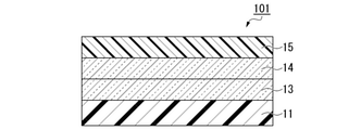
- FIG. 1 is a cross-sectional view for explaining an example of the optical laminate of the present embodiment.
- the optical laminate 101 of the present embodiment is formed by laminating a transparent base material 11, an adhesion layer 13, an optical functional layer 14, and an antifouling layer 15 in order.
- the adhesion layer 13 is a layer that develops adhesion.
- the optical function layer 14 is a layer that expresses an optical function.
- the optical function is a function for controlling reflection, transmission, and refraction, which are the properties of light, and examples thereof include an antireflection function, a selective reflection function, and a lens function.
- the optical functional layer 14 preferably contains any one selected from the antireflection layer and the selective reflection layer.
- the antireflection layer, the selective reflection layer, and the antiglare layer known ones can be used.
- the antireflection layer, the selective reflection layer, and the antiglare layer may be a single layer, or may be a laminated body of a plurality of layers.
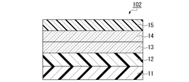
- FIG. 2 is a cross-sectional view showing another example of the optical laminate of the present embodiment.
- the optical laminate 102 shown in FIG. 2 is formed by laminating a transparent base material 11, a hard coat layer 12, an adhesion layer 13, an optical functional layer 14, and an antifouling layer 15 in this order.
- the adhesion layer 13 is a layer that develops adhesion.
- the optical function layer 14 is a layer that expresses an optical function.
- the optical function is a function of controlling reflection, transmission, and refraction, which are the properties of light, and examples thereof include an antireflection function and a selective reflection function lens function.
- the optical functional layer 14 preferably contains any one selected from the antireflection layer and the selective reflection layer.
- Known antireflection layers and selective reflection layers can be used. Both the antireflection layer and the selective reflection layer may be a single layer, or may be a laminated body of a plurality of layers.
- FIG. 3 is a cross-sectional view showing another example of the optical laminate of the present embodiment.
- the optical laminate 10 shown in FIG. 3 is provided with an antireflection layer as the optical functional layer 14 in the optical laminate 102 shown in FIG. 2.
- the optical functional layer 14 (antireflection layer) is composed of a laminated body in which low refractive index layers 14b and high refractive index layers 14a are alternately laminated.
- the optical functional layer 14 shown in FIG. 2 has a hard coat layer 12, an adhesion layer 13, a high refractive index layer 14a, a low refractive index layer 14b, a high refractive index layer 14a, and a low refractive index layer 14b in order from the transparent substrate 11 side.
- the antifouling layer 15 is laminated in this order. Therefore, the antifouling layer 15 is in contact with the low refractive index layer 14b of the optical functional layer 14.
- the transparent base material 11 may be formed of a transparent material capable of transmitting light in the visible light region.
- a plastic film is preferably used as the transparent base material 11.
- the constituent materials of the plastic film include polyester resin, acetate resin, polyether sulfone resin, polycarbonate resin, polyamide resin, polyimide resin, polyolefin resin, (meth) acrylic resin, and polychloride.
- examples thereof include vinyl-based resins, polyvinylidene chloride-based resins, polystyrene-based resins, polyvinyl alcohol-based resins, polyallylate-based resins, and polyphenylene sulfide-based resins.
- transparent material means a material having a light transmittance of 80% or more in the wavelength range used, as long as the effect of the present invention is not impaired.
- (meth) acrylic means methacrylic and acrylic.
- the transparent base material 11 may contain a reinforcing material as long as the optical characteristics are not significantly impaired.
- the reinforcing material is, for example, cellulose nanofiber, nanosilica, or the like.
- polyester-based resins, acetate-based resins, polycarbonate-based resins, and polyolefin-based resins are preferably used as reinforcing materials.
- a triacetyl cellulose (TAC) base material is preferably used as a reinforcing material.
- a glass film which is an inorganic base material can also be used as the transparent base material 11.
- the plastic film is a TAC base material
- the hard coat layer 12 is formed on one surface side thereof, a permeation layer is formed in which a part of the components constituting the hard coat layer 12 permeates.
- the adhesion between the transparent base material 11 and the hard coat layer 12 is improved, and the generation of interference fringes due to the difference in refractive index between the layers can be suppressed.
- the transparent base material 11 may be a film to which an optical function and / or a physical function is imparted.
- films having optical and / or physical functions include polarizing plates, retardation compensation films, heat ray blocking films, transparent conductive films, brightness improving films, barrier property improving films, and the like.
- the thickness of the transparent base material 11 is not particularly limited, but is preferably 25 ⁇ m or more, for example.
- the film thickness of the transparent substrate 11 is more preferably 40 ⁇ m or more.
- the thickness of the transparent base material 11 is 25 ⁇ m or more, the rigidity of the base material itself is ensured, and wrinkles are less likely to occur even if stress is applied to the optical laminate 10.
- the thickness of the transparent base material 11 is 25 ⁇ m or more, even if the hard coat layer 12 is continuously formed on the transparent base material 11, wrinkles are less likely to occur and there is less concern in manufacturing, which is preferable.
- the thickness of the transparent base material 11 is 40 ⁇ m or more, wrinkles are less likely to occur, which is preferable.
- the thickness of the transparent base material 11 is preferably 1000 ⁇ m or less, and more preferably 600 ⁇ m or less.
- the thickness of the transparent base material 11 is 1000 ⁇ m or less, it is easy to wind the optical laminate 10 in the middle of production and the optical laminate 10 after production in a roll shape, and the optical laminate 10 can be efficiently manufactured.
- the optical laminate 10 can be made thinner and lighter.
- the thickness of the transparent base material 11 is 600 ⁇ m or less, the optical laminate 10 can be manufactured more efficiently, and the thin film and the weight can be further reduced, which is preferable.
- the surface of the transparent substrate 11 may be subjected to etching treatment such as sputtering, corona discharge, ultraviolet irradiation, electron beam irradiation, chemical formation, oxidation, and / or undercoating treatment in advance. By performing these treatments in advance, the adhesion to the hard coat layer 12 formed on the transparent substrate 11 can be improved. Further, before forming the hard coat layer 12 on the transparent base material 11, the surface of the transparent base material 11 is subjected to solvent cleaning, ultrasonic cleaning, or the like, if necessary, so that the surface of the transparent base material 11 can be washed. It is also preferable to remove dust and clean it.
- etching treatment such as sputtering, corona discharge, ultraviolet irradiation, electron beam irradiation, chemical formation, oxidation, and / or undercoating treatment in advance.
- the hard coat layer 12 may be made of only a binder resin, or may contain a filler together with the binder resin as long as the transparency is not impaired.
- the filler one made of an organic substance may be used, one made of an inorganic substance may be used, or one made of an organic substance and an inorganic substance may be used.
- the binder resin used for the hard coat layer 12 is preferably a transparent resin, and for example, an ionized radiation curable resin, a thermoplastic resin, a thermosetting resin, or the like, which is a resin that can be cured by ultraviolet rays or electron beams, may be used. can.
- Examples of the ionizing radiation curable resin used for the binder resin of the hard coat layer 12 include ethyl (meth) acrylate, ethylhexyl (meth) acrylate, styrene, methylstyrene, N-vinylpyrrolidone and the like.
- Examples of the compound which is an ionizing radiation curable resin having two or more unsaturated bonds include trimethyl propanetri (meth) acrylate, tripropylene glycol di (meth) acrylate, diethylene glycol di (meth) acrylate, and dipropylene.
- Glycoldi (meth) acrylate pentaerythritol tri (meth) acrylate, pentaerythritol tetra (meth) acrylate, dipentaerythritol hexa (meth) acrylate, 1,6-hexanediol di (meth) acrylate, neopentyl glycol di (meth) ) Acrylate, Trimethylol Propanetri (meth) Acrylate, Ditrimethylol Propanetetra (meth) Acrylate, Dipentaerythritol Penta (Meta) Acrylate, Tripentaerythritol Octa (Meta) Acrylate, Tetrapentaerythritol Deca (Meta) Acrylate, Isothianulic Acid Tri (meth) acrylate, isocyanuric acid di (meth) acrylate, polyester tri (meth) acrylate, polyester di (meth) acryl
- pentaerythritol triacrylate PETA
- dipentaerythritol hexaacrylate DPHA
- pentaerythritol tetraacrylate PETA
- (meth) acrylate refers to methacrylate and acrylate.
- a resin obtained by modifying the above-mentioned compound with PO (propylene oxide), EO (ethylene oxide), CL (caprolactone) or the like can also be used as the ionizing radiation curable resin.
- thermoplastic resin used for the binder resin of the hard coat layer 12 examples include a styrene resin, a (meth) acrylic resin, a vinyl acetate resin, a vinyl ether resin, a halogen-containing resin, an alicyclic olefin resin, and a polycarbonate resin.
- examples thereof include resins, polyester resins, polyamide resins, cellulose derivatives, silicone resins and rubbers or elastomers.
- the thermoplastic resin is preferably non-crystalline and soluble in an organic solvent (particularly a common solvent capable of dissolving a plurality of polymers and curable compounds).
- styrene-based resin (meth) acrylic-based resin, alicyclic olefin-based resin, polyester-based resin, cellulose derivative (cellulose ester, etc.) and the like are preferable.
- thermosetting resin used for the binder resin of the hard coat layer 12 examples include phenol resin, urea resin, diallyl phthalate resin, melamine resin, guanamine resin, unsaturated polyester resin, polyurethane resin, epoxy resin, aminoalkyd resin and melamine.
- phenol resin urea resin
- diallyl phthalate resin diallyl phthalate resin
- melamine resin guanamine resin
- unsaturated polyester resin polyurethane resin
- epoxy resin epoxy resin
- aminoalkyd resin and melamine examples of the thermosetting resin used for the binder resin of the hard coat layer 12
- -Urea cocondensation resin silicon resin
- polysiloxane resin including so-called silsesquioxane such as cage-like and ladder-like
- the hard coat layer 12 may contain an organic resin and an inorganic material, or may be an organic-inorganic hybrid material.
- the one formed by the sol-gel method can be mentioned.
- the inorganic material include silica, alumina, zirconia, and titania.
- the organic material include acrylic resin.
- Various fillers contained in the hard coat layer 12 can be selected depending on the use of the optical laminate 10 from the viewpoints of antiglare property, adhesion to the optical functional layer 14 described later, and anti-blocking property. Specifically, for example, known particles such as silica (Si oxide) particles, alumina (aluminum oxide) particles, and organic fine particles can be used.
- the hard coat layer 12 may contain, for example, a binder resin and silica particles and / or alumina particles as a filler. By dispersing silica particles and / or alumina particles as a filler in the hard coat layer 12, fine irregularities can be formed on the surface of the hard coat layer 12. These silica particles and / or alumina particles may be exposed on the surface of the hard coat layer 12 on the optical functional layer 14 side. In this case, the binder resin of the hard coat layer 12 and the optical functional layer 14 are strongly bonded. Therefore, the adhesion between the hard coat layer 12 and the optical functional layer 14 is improved, the hardness of the hard coat layer 12 is increased, and the scratch resistance of the optical laminate 10 is improved.
- the average particle size of the filler of the hard coat layer 12 is, for example, 800 nm or less, preferably 780 nm or less, and more preferably 100 nm or less.
- the filler of the size for example, silica particles, alumina particles and the like are preferably used.
- the haze value of the entire optical laminate 10 is 2% or less.
- the optical laminate 10 having a haze of 2% or less has high transparency and is a so-called clear type antireflection film.
- the average particle size of the filler of the hard coat layer 12 may be, for example, 0.5 ⁇ m or more.
- the filler of the size for example, organic fine particles such as acrylic resin are preferably used.
- the haze value of the entire optical laminate 10 is more than 2%.
- the optical laminate 10 having a haze of more than 2% has antiglare properties and is a so-called antiglare (AG) type antireflection film.
- the average particle size of the filler is preferably 10 ⁇ m or less, more preferably 5 ⁇ m or less, and particularly preferably 3 ⁇ m or less.
- various reinforcing materials can be used in order to impart toughness to the hard coat layer 12 as long as the optical characteristics are not impaired. Examples of the reinforcing material include cellulose nanofibers.
- the thickness of the hard coat layer 12 is not particularly limited, but is preferably 0.5 ⁇ m or more, more preferably 1 ⁇ m or more, for example.
- the thickness of the hard coat layer 12 is preferably 100 ⁇ m or less.
- the thickness of the hard coat layer 12 is 0.5 ⁇ m or more, sufficient hardness can be obtained, so that scratches in manufacturing are less likely to occur.
- the optical laminate 10 can be made thinner and lighter.
- the thickness of the hard coat layer 12 is 100 ⁇ m or less, microcracks of the hard coat layer 12 generated when the optical laminate 10 in the process of manufacturing is bent are less likely to occur, and the productivity is improved.
- the hard coat layer 12 may be a single layer or may be a stack of a plurality of layers. Further, the hard coat layer 12 may be further provided with known functions such as ultraviolet absorption performance, antistatic performance, refractive index adjustment function, and hardness adjustment function. Further, the function imparted to the hard coat layer 12 may be imparted to a single hard coat layer, or may be imparted to a plurality of layers separately.
- the adhesion layer 13 is a layer formed to improve the adhesion between the transparent base material 11 or the hard coat layer 12 which is an organic film and the optical functional layer 14 which is an inorganic film.
- an adhesion layer 13 is provided between the hard coat layer 12 and the optical functional layer 14.
- the adhesion layer 13 has a function of bringing the hard coat layer 12 and the optical functional layer 14 into close contact with each other.
- the adhesion layer 13 is preferably made of an oxygen-deficient metal oxide or metal.
- the oxygen-deficient metal oxide is a metal oxide in which the number of oxygen is insufficient compared to the stoichiometric composition.
- oxygen-deficient metal oxide examples include SiOx, AlOx, TiOx, ZrOx, CeOx, MgOx, ZnOx, TaOx, SbOx, SnOx, MnOx and the like.
- the metal examples include Si, Al, Ti, Zr, Ce, Mg, Zn, Ta, Sb, Sn, Mn, In and the like.
- the adhesion layer 13 may be, for example, one in which x in SiOx is more than 0 and less than 2.0. Further, the adhesion layer may be formed of a mixture of a plurality of kinds of metals or metal oxides.
- the thickness of the adhesion layer is preferably more than 0 nm and 20 nm or less, and particularly preferably 1 nm or more and 10 nm or less, from the viewpoint of maintaining transparency and adhesion to the optical functional layer and obtaining good optical characteristics.
- the optical functional layer 14 is a laminated body that exhibits an antireflection function.
- the optical functional layer 14 shown in FIG. 3 is a laminated body having a total of four layers in which high refractive index layers 14a and low refractive index layers 14b are alternately laminated in order from the close contact layer 13 side.
- the number of layers of the high refractive index layer 14a and the low refractive index layer 14b is not particularly limited, and the number of layers of the high refractive index layer 14a and the low refractive index layer 14b can be any number.
- the optical functional layer 14 is composed of a laminated body in which the low refractive index layer 14b and the high refractive index layer 14a are alternately laminated, it is incident from the antifouling layer 15 side.
- the light is diffused by the optical functional layer 14. Therefore, an antireflection function for preventing light incident from the antifouling layer 15 side from being reflected in one direction can be obtained.
- the low index of refraction layer 14b contains, for example, an oxide of a metal.
- the low refractive index layer 14b may contain an oxide of Si from the viewpoint of easy availability and cost, and is preferably a layer containing SiO 2 (oxide of Si) or the like as a main component.
- the SiO 2 monolayer film is colorless and transparent.
- the main component of the low refractive index layer 14b means a component contained in the low refractive index layer 14b in an amount of 50% by mass or more.
- the low refractive index layer 14b is a layer containing an oxide of Si as a main component, it may contain another element of less than 50% by mass.
- the content of the element other than the oxide of Si is preferably 10% or less.
- Na may be contained for the purpose of improving durability, Zr, Al, or N for the purpose of improving hardness, and Zr, Al for the purpose of improving alkali resistance.
- the refractive index of the low refractive index layer 14b is preferably 1.20 to 1.60, and more preferably 1.30 to 1.50.
- Examples of the dielectric used for the low refractive index layer 14b include magnesium fluoride (MgF 2 , refractive index 1.38) and the like.
- the refractive index of the high refractive index layer 14a is preferably 2.00 to 2.60, and more preferably 2.10 to 2.45.
- the dielectrics used for the high refractive index layer 14a include niobide pentoxide (Nb 2 O 5 , refractive index 2.33), titanium oxide (TiO 2 , refractive index 2.33 to 2.55), and tungsten oxide (WO).
- Refractive index 2.2 Celium oxide (CeO 2 , Refractive index 2.2), Tantalum pentoxide (Ta 2 O 5 , Refractive index 2.16), Zinc oxide (ZnO, Refractive index 2.1), Examples thereof include indium tin oxide (ITO, refractive index 2.06), zirconium oxide (ZrO 2 , refractive index 2.2) and the like.
- ITO indium tin oxide
- IZO indium zinc oxide
- the optical functional layer 14 for example, it is preferable to use a high refractive index layer 14a made of niobium pentoxide (Nb 2 O 5 , refractive index 2.33) and a low refractive index layer 14b made of SiO 2. ..
- the film thickness of the low refractive index layer 14b may be in the range of 1 nm or more and 200 nm or less, and is appropriately selected depending on the wavelength range in which the antireflection function is required.
- the film thickness of the high refractive index layer 14a may be, for example, 1 nm or more and 200 nm or less, and is appropriately selected depending on the wavelength range in which the antireflection function is required.
- the film thicknesses of the high refractive index layer 14a and the low refractive index layer 14b can be appropriately selected according to the design of the optical functional layer 14, respectively.
- the high refractive index layer 14a of 5 to 50 nm, the low refractive index layer 14b of 10 to 80 nm, the high refractive index layer 14a of 20 to 200 nm, and the low refractive index layer 14b of 50 to 200 nm are used in this order from the close contact layer 13 side. be able to.
- the low refractive index layer 14b is arranged on the antifouling layer 15 side.
- the antireflection performance of the optical functional layer 14 is good, which is preferable.
- the antifouling layer 15 is formed on the outermost surface of the optical functional layer 14 to prevent the optical functional layer 14 from being soiled. Further, when the antifouling layer 15 is applied to a touch panel or the like, the wear resistance of the antifouling layer 15 suppresses the wear of the optical functional layer 14.
- the antifouling layer 15 of the present embodiment is made of, for example, a vapor-deposited film on which an antifouling material is vapor-deposited.
- the antifouling layer 15 is formed by vacuum-depositing a fluorine-based organic compound as an antifouling material on one surface of the low refractive index layer 14b constituting the optical functional layer 14. In the present embodiment, since the antifouling material contains a fluorine-based organic compound, the optical laminate 10 has even better abrasion resistance and alkali resistance.
- a compound composed of a fluorine-modified organic group and a reactive silyl group for example, alkoxysilane
- examples of commercially available products include Optool DSX (manufactured by Daikin Corporation) and KY-100 series (manufactured by Shin-Etsu Chemical Co., Ltd.).
- the fluorine-based organic compound constituting the antifouling layer 15 a compound composed of a fluorine-modified organic group and a reactive silyl group (for example, alkoxysilane) is used as the fluorine-based organic compound, and the optical contact with the antifouling layer 15 is optical.
- a low refractive index layer 14b of the functional layer 14 a case of using one made of SiO 2, siloxane bonds are formed between the silanol group and SiO 2 and a skeleton of the fluorine-based organic compound. Therefore, the adhesion between the optical functional layer 14 and the antifouling layer 15 is good, which is preferable.
- the optical thickness of the antifouling layer 15 may be in the range of 1 nm or more and 20 nm or less, preferably 3 nm or more and 10 nm or less.
- the thickness of the antifouling layer 15 is 1 nm or more, sufficient wear resistance can be ensured when the optical laminate 10 is applied to a touch panel application or the like. Further, when the thickness of the antifouling layer 15 is 20 nm or less, the time required for vapor deposition is short and efficient production can be performed.
- the surface roughness Ra of the antifouling layer 15 differs depending on the use and configuration of the optical laminate.
- the surface roughness Ra of the antifouling layer 15 is preferably 3 nm or more, for example.
- the upper limit is not particularly limited, but is preferably 9 nm or less from the viewpoint of scratch resistance, for example.
- the surface roughness Ra of the antifouling layer 15 is preferably, for example, 10 nm or more, preferably 30 nm or more. It is more preferable to have.
- the surface roughness Ra of the antifouling layer 15 referred to here is a value before the scratch resistance test is performed.
- the average length RSm of the elements of the antifouling layer 15 varies depending on the application and configuration of the optical laminate.
- the average length RSm of the elements of the antifouling layer 15 is preferably 59 nm or more, for example. It is more preferably 92 nm or less.
- the average length RSm of the elements of the antifouling layer 15 referred to here is a value before the scratch resistance test is performed.
- the antifouling layer 15 includes a light stabilizer, an ultraviolet absorber, a colorant, an antistatic agent, a lubricant, a leveling agent, an antifoaming agent, an antioxidant, a flame retardant, an infrared absorber, a surfactant and the like, if necessary. May contain the additive of.
- the antifouling layer 15 formed by thin film deposition is firmly bonded to the optical functional layer 14 and has few voids and is dense. As a result, the antifouling layer 15 of the present embodiment exhibits different characteristics from the antifouling layer formed by a conventional method such as application of an antifouling material.
- the antifouling layer 15 of the clear type optical laminate 10 of the present embodiment has the following characteristics. (1) The contact angle difference with respect to water after the scratch resistance test by reciprocating steel wool 500 times horizontally is 12 ° or less. (2) The contact angle with water after the scratch resistance test by reciprocating steel wool 500 times horizontally is 109 ° or more.
- L0 * , a0 * , and b0 * are the values before the scratch resistance test, and L1 * , a1 * , and b1 * are the values after the scratch resistance test.
- L * represented by the following formula (4) by SCE (Specular Component Exclude, a method for measuring reflected color that does not take specular reflected light into consideration) before and after the scratch resistance test by moving steel wool horizontally reciprocating 500 times.
- the amount of change in the a * b * value ( ⁇ E value) is 0.5 or less.
- L0 * , a0 * , and b0 * are the values before the scratch resistance test
- L1 * , a1 * , and b1 * are the values after the scratch resistance test.
- the residual fluorine rate measured by fluorescent X-ray analysis (XRF) after immersion in a NaOH solution (liquid temperature 55 ° C.) having a concentration of 0.1 mol / L for 4 hours is 70% or more.
- the fluorine residual rate measured by the fluorescent X-ray analysis method (XRF) after the ultrasonic cleaning test is 79% or more.
- the antifouling layer 15 of the AG-type optical laminate 10 of the present embodiment has the following characteristics.
- (1) The fluorine residual rate measured by an X-ray photoelectron spectrophotometer (ESCA) after the scratch resistance test by reciprocating a waste cloth (nonwoven fabric wiper) 4000 times is 78% or more.
- (3) The fluorine residual rate measured by the fluorescent X-ray analysis method (XRF) after the ultrasonic cleaning test is 77% or more.
- the optical laminate 10 provided with the antifouling layer 15 of the present embodiment formed by thin film deposition has fewer voids and is densely formed as compared with the antifouling layer formed by coating. Further, in the optical laminate 10 of the present embodiment, the antifouling layer 15 is firmly bonded to the low refractive index layer 14b in contact with the antifouling layer 15. Therefore, the optical laminate 10 of the present embodiment has excellent visible light transmission, can maintain high wear resistance against repeated friction, and can maintain high resistance to alkali resistance.
- the optical laminate 10 of the present embodiment shown in FIG. 3 can be manufactured, for example, by the method shown below.
- the method for manufacturing the optical laminate 10 a case where the optical laminate 10 is manufactured using the transparent base material 11 wound in a roll shape will be described as an example.
- the transparent base material 11 wound in a roll shape is unwound.
- a slurry containing the material to be the hard coat layer 12 is applied onto the transparent substrate 11 by a known method, and the slurry is cured by a known method corresponding to the material to be the hard coat layer 12.
- the hard coat layer 12 is formed (hard coat layer forming step).
- the transparent base material 11 having the hard coat layer 12 formed on the surface thereof is wound into a roll by a known method.
- an adhesion layer forming step for forming the adhesion layer 13 and an optical functional layer forming step for forming the optical functional layer 14 are performed on the hard coat layer 12.
- an antifouling layer forming step of forming the antifouling layer 15 on the optical functional layer 14 is performed.
- the first surface treatment step, the adhesion layer forming step, the optical functional layer forming step, the second surface treatment step, and the antifouling layer forming step are in the process of manufacturing the optical laminate. It is preferable to carry out continuously while maintaining the state under reduced pressure.
- the first surface treatment step, the adhesion layer forming step, the optical functional layer forming step, the second surface treatment step, and the antifouling layer forming step are continuously performed while maintaining the optical laminate in the process of being manufactured under reduced pressure.
- a sputtering apparatus an apparatus provided with the thin film forming apparatus described in Patent Document 4 can be used.
- the manufacturing apparatus 20 shown in FIG. 4 includes a roll unwinding device 4, a pretreatment device 2A, a sputtering device 1, a pretreatment device 2B, a vapor deposition device 3, and a roll winding device 5. As shown in FIG. 4, these devices 4, 2A, 1, 2B, 3, and 5 are connected in this order.
- the manufacturing apparatus 20 shown in FIG. 4 unwinds the base material from the roll and continuously passes the connected apparatus (in FIG. 4, the pretreatment apparatus 2A, the sputtering apparatus 1, the pretreatment apparatus 2B, and the vapor deposition apparatus 3). It is a roll-to-roll type manufacturing apparatus that continuously forms a plurality of layers on a base material by winding it afterwards.
- the transport speed (line speed) of the optical laminate 10 in the middle of manufacturing can be appropriately set.
- the transport speed is preferably, for example, 0.5 to 20 m / min, more preferably 0.5 to 10 m / min.
- the roll unwinding device 4 shown in FIG. 4 includes a chamber 34 having a predetermined decompression atmosphere inside, and one or a plurality of vacuum pumps 21 (in FIG. 4 in FIG. 4) for discharging gas in the chamber 34 to create a decompression atmosphere. It has one) and an unwinding roll 23 and a guide roll 22 installed in the chamber 34. As shown in FIG. 4, the chamber 34 is connected to the chamber 31 of the sputtering device 1 via the pretreatment device 2A. A transparent base material 11 having a hard coat layer 12 formed on its surface is wound around the unwinding roll 23. The unwinding roll 23 supplies the transparent base material 11 having the hard coat layer 12 formed on the surface to the pretreatment device 2A at a predetermined transport speed.
- the pretreatment device 2A shown in FIG. 4 has a chamber 32 having a predetermined depressurized atmosphere inside, a can roll 26, a plurality of guide rolls 22 (two in FIG. 4), and a plasma discharge device 42. As shown in FIG. 4, the can roll 26, the guide roll 22, and the plasma discharge device 42 are installed in the chamber 32. As shown in FIG. 4, the chamber 32 is connected to the chamber 31 of the sputtering apparatus 1.
- the can roll 26 and the guide roll 22 conveyed the transparent base material 11 on which the hard coat layer 12 sent from the roll unwinding device 4 was formed at a predetermined transfer speed, and the surface of the hard coat layer 12 was treated.
- the transparent substrate 11 is sent to the sputtering apparatus 1.
- the plasma discharge device 42 is arranged to face the outer peripheral surface of the can roll 26 at a predetermined interval.
- the plasma discharge device 42 ionizes the gas by glow discharge.
- the gas is preferably inexpensive, inert and does not affect the optical characteristics, and for example, argon gas, oxygen gas, nitrogen gas, helium gas and the like can be used.
- the gas it is preferable to use argon gas because it has a large mass, is chemically stable, and is easily available.
- a glow discharge device for ionizing argon gas with high-frequency plasma as the plasma discharge device 42.
- the sputtering apparatus 1 shown in FIG. 4 includes a chamber 31 having a predetermined depressurized atmosphere inside, and one or a plurality of vacuum pumps 21 (two in FIG. 4) that discharge gas in the chamber 31 to create a depressurized atmosphere. ), A plurality of (two in FIG. 4) guide rolls 22, and a plurality of (four in the example shown in FIG. 4) film forming portions 41. As shown in FIG. 4, the film forming roll 25, the guide roll 22, and the film forming section 41 are installed in the chamber 31. As shown in FIG. 4, the chamber 31 is connected to the chamber 32 of the pretreatment device 2B.
- the film forming roll 25 and the guide roll 22 convey the transparent base material 11 on which the surface-treated hard coat layer 12 is formed, which is sent from the pretreatment device 2A, on the hard coat layer 12 at a predetermined transfer speed.
- the transparent base material 11 on which the adhesion layer 13 and the optical functional layer 14 are formed is supplied to the pretreatment device 2B.
- the adhesion layer 13 is laminated on the hard coat layer 12 of the transparent substrate 11 running on the film forming roll 25 by sputtering, and the high refractive index layer 14a and the low refractive index are laminated on the adhesion layer 13.
- the layers 14b are alternately laminated to form the optical functional layer 14.
- a plurality of film forming portions 41 are arranged so as to face the outer peripheral surface of the film forming roll 25 at a predetermined interval and are provided so as to surround the film forming roll 25.
- the number of film forming portions 41 is determined according to the total number of layers of the adhesion layer 13, the high refractive index layer 14a forming the optical functional layer 14, and the low refractive index layer 14b.
- a plurality of film forming rolls 25 may be provided in the chamber 31, and the film forming section 41 may be arranged around each film forming roll 25.
- a guide roll 22 may be further provided if necessary.
- a plurality of chambers 31 provided with the film forming roll 25 and the film forming portion 41 may be connected. Further, the diameter of the film forming roll 25 may be appropriately changed in order to facilitate the securing of the distance between the adjacent film forming portions 41.
- a predetermined target (not shown) is installed in each film forming portion 41.
- a voltage is applied to the target by a known structure.
- a gas supply unit (not shown) that supplies a predetermined reactive gas and a carrier gas to the target at a predetermined flow rate in the vicinity of the target, and a known magnetic field generation source that forms a magnetic field on the surface of the target (not shown). (Not shown) is provided.
- the type and flow rate of the target material and the reactive gas are determined by passing between the film forming portion 41 and the film forming roll 25 to form the adhesion layer 13 and the high refractive index layer 14a on the transparent substrate 11. It is appropriately determined according to the composition of the low refractive index layer 14b. For example, when forming a layer made of SiO 2 , Si is used as a target and O 2 is used as a reactive gas. Further, for example, when forming a layer made of Nb 2 O 5 , Nb is used as a target and O 2 is used as a reactive gas.
- the magnetron sputtering method is not limited to the magnetron sputtering method, and a two-pole sputtering method using plasma generated by DC glow discharge or high frequency, a three-pole sputtering method to add a hot cathode, or the like may be used. ..
- the sputtering apparatus 1 includes an optical monitor (not shown) as a measuring unit for measuring optical characteristics after forming a film of each layer to be the adhesion layer 13 and the optical functional layer 14. Thereby, the quality of the formed adhesion layer 13 and the optical functional layer 14 can be confirmed.
- an optical monitor not shown
- Examples of the optical monitor include those that measure the optical characteristics in the width direction of the adhesion layer 13 and the optical functional layer 14 formed on the hard coat layer 12 by an optical head capable of scanning in the width direction. Be done.
- an optical monitor for example, by measuring the peak wavelength of reflectance as an optical characteristic and converting it into an optical thickness, the optical thickness distribution in the width direction of the adhesion layer 13 and the optical functional layer 14 can be obtained. Can be measured.
- By measuring the optical characteristics using an optical monitor it is possible to form an optical laminate 10 having an adhesion layer 13 and an optical functional layer 14 having optimum optical characteristics while adjusting spatter conditions in real time.
- the pretreatment device 2B shown in FIG. 4 has a chamber 32 having a predetermined depressurized atmosphere inside, a can roll 26, a plurality of guide rolls 22 (two in FIG. 4), and a plasma discharge device 42. As shown in FIG. 4, the can roll 26, the guide roll 22, and the plasma discharge device 42 are installed in the chamber 32. As shown in FIG. 4, the chamber 32 is connected to the chamber 33 of the vapor deposition apparatus 3.
- the can roll 26 and the guide roll 22 convey the transparent base material 11 on which each layer is formed up to the optical functional layer 14 sent from the sputtering apparatus 1 at a predetermined conveying speed, and the surface of the optical functional layer 14 is treated.
- the transparent substrate 11 is sent to the vapor deposition apparatus 3.
- the plasma discharge device 42 for example, the same one as the pretreatment device 2A can be used.
- the plasma discharge device 42 ionizes the gas by glow discharge.
- the gas is preferably inexpensive, inert and does not affect the optical characteristics, and for example, argon gas, oxygen gas, nitrogen gas, helium gas and the like can be used.
- Argon gas or oxygen gas has a large effect on the surface of the optical functional layer 14. In particular, when argon gas having a large mass is used, it is easy to adjust the surface roughness Ra of the optical functional layer 14 or the average length RSm of the element.
- the thin-film deposition apparatus 3 shown in FIG. 4 includes a chamber 33 having a predetermined decompression atmosphere inside, and one or a plurality of vacuum pumps 21 (one in FIG. 4) for discharging the gas in the chamber 33 to create a decompression atmosphere. ), A plurality of (four in FIG. 4) guide rolls 22, a vapor deposition source 43, and a heating device 53. As shown in FIG. 4, the guide roll 22 and the vapor deposition source 43 are installed in the chamber 33.
- the chamber 33 is connected to the chamber 35 of the roll winding device 5.
- the thin-film deposition source 43 is arranged to face the transparent base material 11 whose surface of the optical functional layer 14 has been treated, which is conveyed substantially horizontally between two adjacent guide rolls 22.
- the thin-film deposition source 43 supplies an evaporative gas made of a material to be the antifouling layer 15 onto the optical functional layer 14.
- the orientation of the vapor deposition source 43 can be arbitrarily set.
- the heating device 53 heats the material to be the antifouling layer 15 to a vapor pressure temperature.
- a resistance heating method, a heater heating method, an induction heating method, an electron beam method, or the like can be used as the heating device 53.
- a container containing an antifouling material to be the antifouling layer 15 is energized and heated as a resistor.
- the container is heated by a heater arranged on the outer circumference of the container.
- the container or the antifouling material is heated by the electromagnetic induction action from the induction coil installed outside.
- the thin-film deposition apparatus 3 shown in FIG. 4 has a guide plate (not shown) that guides the vaporized material vaporized by the vapor deposition source 43 to a predetermined position, and a film thickness meter (not shown) that observes the thickness of the antifouling layer 15 formed by the vapor deposition. It includes a vacuum pressure gauge (not shown) for measuring the pressure in the chamber 33 (not shown), and a power supply device (not shown).
- the guide plate may have any shape as long as the vaporized vaporized material can be guided to a desired position. The guide plate may not be provided if it is not necessary.
- the vacuum pressure gauge for example, an ion gauge or the like can be used.
- the power supply device include a high frequency power supply.
- the roll winding device 5 shown in FIG. 4 includes a chamber 35 having a predetermined depressurized atmosphere inside, and one or a plurality of vacuum pumps 21 (in FIG. 4 in FIG. 4) for discharging gas in the chamber 35 to create a depressurized atmosphere. It has one) and a take-up roll 24 and a guide roll 22 installed in the chamber 35.
- the take-up roll 24 is wound with a transparent base material 11 (optical laminate 10) having each layer up to the antifouling layer 15 formed on the surface thereof.
- the take-up roll 24 and the guide roll 22 take up the optical laminate 10 at a predetermined take-up speed. If necessary, a carrier film may also be used.
- the vacuum pump 21 provided in the manufacturing apparatus 20 shown in FIG. 4 for example, a dry pump, an oil rotary pump, a turbo molecular pump, an oil diffusion pump, a cryo pump, a sputter ion pump, a getter pump, or the like can be used. ..
- the vacuum pump 21 can be appropriately selected or used in combination in each of the chambers 31, 32, 33, 34 and 35 to create a desired depressurized state.
- the vacuum pump 21 only needs to be able to maintain both the chamber 31 of the sputtering apparatus 1 and the chamber 33 of the vapor deposition apparatus 3 in a desired depressurized state, and the installation position and number of the vacuum pumps 21 in the manufacturing apparatus 20 are not particularly limited. Further, in the manufacturing apparatus 20 shown in FIG. 4, a roll unwinding device 4, a pretreatment device 2A, a sputtering device 1, a pretreatment device 2B, a vapor deposition device 3, and a roll winding device 5 are connected to each other.
- the vacuum pump 21 may be installed in the chambers 31, 32, 33, 34, 35, respectively, and both the chamber 31 of the sputtering apparatus 1 and the chamber 33 of the vapor deposition apparatus 3 are maintained in a desired depressurized state. If possible, it may be installed in only a part of the chambers 31, 32, 33, 34, 35.
- the first surface treatment step, the adhesion layer forming step, the optical functional layer forming step, the second surface treatment step, and the antifouling layer forming step are performed on the optical laminate in the middle of manufacturing.
- a method of continuously performing 10 while maintaining the state under reduced pressure will be described.
- the unwinding roll 23 around which the transparent base material 11 having the hard coat layer 12 formed on the surface is wound is installed.
- the unwinding roll 23 and the guide roll 22 are rotated to feed the transparent base material 11 having the hard coat layer 12 formed on the surface to the pretreatment device 2A at a predetermined transport speed.
- a first surface treatment step is performed as a pretreatment for the surfaces on which the adhesion layer 13 and the optical functional layer 14 are formed.
- the first surface treatment step is performed on the transparent base material 11 on which the hard coat layer 12 is formed.
- the can roll 26 and the guide roll 22 are rotated to transport the transparent base material 11 on which the hard coat layer 12 is formed at a predetermined transport speed, and the hard is run on the can roll 26.
- the surface of the coat layer 12 is treated.
- the surface treatment method of the hard coat layer 12 for example, glow discharge treatment, plasma treatment, ion etching, alkali treatment and the like can be used. Among these, it is preferable to use the glow discharge treatment because a large area treatment is possible.
- the glow discharge treatment can be performed, for example, with a treatment intensity of 0.1 to 10 kwh.
- the adhesion layer forming step and the optical functional layer forming step are performed in the chamber 31 of the sputtering apparatus 1. Specifically, the hard film traveling on the film forming roll 25 while rotating the film forming roll 25 and the guide roll 22 to convey the transparent base material 11 on which the hard coat layer 12 is formed at a predetermined conveying speed. The adhesion layer 13 and the optical functional layer 14 are formed on the coat layer 12.
- the adhesion layer 13 is formed by sputtering by changing the type and flow rate of the target material installed in each film forming section 41 or the reactive gas supplied from the gas supply section, and the adhesion layer 13 is formed on the adhesive layer 13.
- the high refractive index layer 14a and the low refractive index layer 14b are alternately laminated. That is, the adhesion layer forming step and the optical functional layer forming step are continuously performed in the sputtering apparatus 1. As a result, the adhesion layer 13 and the optical functional layer 14 which is an antireflection layer are formed.
- the film When forming a SiO x film as the adhesion layer 13, it is preferable to form the film by reactive sputtering using a mixed gas atmosphere of oxygen gas and argon gas using a silicon target.
- the adhesion layer 13 the high refractive index layer 14a, and the low refractive index layer 14b are continuously laminated by sputtering, the adhesion layer 13 is formed, the high refractive index layer 14a is formed, and the low refractive index layer 14b is formed.
- the target material may be changed depending on the time of film formation.
- a layer made of the target material and a layer made of an oxide of the target material are alternately formed and adhered to each other.
- the layer 13, the high refractive index layer 14a, and the low refractive index layer 14b may be used.
- the pressure during sputtering for forming the adhesion layer 13 and the optical functional layer 14 varies depending on the metal to be sputtered, but may be 2 Pa or less, preferably 1 Pa or less, and preferably 0.6 Pa or less. It is more preferably 0.2 Pa or less, and particularly preferably 0.2 Pa or less.
- the pressure during sputtering is 1 Pa or less under reduced pressure, the mean free path of the film-forming molecules becomes long, and the film-forming molecules are laminated while the energy of the film-forming molecules is high, so that the film quality becomes denser and better.
- the transparent base material 11 having the adhesion layer 13 and the optical functional layer 14 formed on the hard coat layer 12 is sent out to the pretreatment device 2B by the rotation of the film forming roll 25 and the guide roll 22.
- a second surface treatment step is performed as a pretreatment for the surface on which the antifouling layer 15 is formed.
- the transparent base material 11 on which the optical functional layer 14 is formed obtained by the optical functional layer forming step is continuously subjected to the second surface treatment while being maintained under reduced pressure without being exposed to the atmosphere. Perform the process.
- the can roll 26 and the guide roll 22 are rotated to transport the transparent base material 11 on which each layer up to the optical functional layer 14 is formed at a predetermined transport speed while transporting the transparent base material 11 on the can roll 26.
- a discharge treatment is performed on the surface of the traveling optical functional layer 14.
- a surface treatment method for the optical functional layer 14 for example, glow discharge treatment, plasma treatment, ion etching, alkali treatment and the like can be used. Among these, it is preferable to use the glow discharge treatment because a large area treatment is possible.
- the glow discharge treatment is preferably performed in an atmosphere of O 2 gas or argon gas. When these gases are used, the surface roughness of the optical functional layer 14 can be easily adjusted. When the surface of the optical functional layer 14 is subjected to an electric discharge treatment, the surface of the optical functional layer 14 is etched and the roughness of the surface of the optical functional layer 14 changes.
- the surface roughness Ra of the optical functional layer 14 can be controlled by setting the integrated output during the discharge process in an appropriate range.
- the integrated output during the discharge process is 130 W ⁇ min / m 2 or more and 2000 W ⁇ min / m 2 or less.
- the integrated output is a value obtained by dividing the product of the glow discharge output irradiated to the optical functional layer 14 and the irradiation time per unit area during the discharge process.
- the conditions for discharge processing can be set as appropriate. By appropriately setting the conditions of the electric discharge treatment, the adhesion between the optical functional layer 14 and the antifouling layer 15 formed on the optical functional layer 14 becomes good, and the optical laminate having further good friction resistance and alkali resistance is obtained. 10 is obtained.
- the surface roughness Ra of the optical functional layer 14 and the average length RSm of the elements after the discharge treatment differ depending on the average length of the surface roughness elements of the hard coat layer 12 provided under the optical functional layer 14. Further, the surface roughness Ra of the optical functional layer 14 and the average length RSm of the elements after the discharge treatment are the surface roughness Ra of the antifouling layer 15 formed on the optical functional layer 14 and the average length RSm of the elements. Affects.
- the surface of the optical functional layer is treated so that the rate of change in surface roughness represented by the following formula (1) is 1 to 25%.
- the surface of the optical functional layer is treated under this condition.
- the integrated output during the discharge process is one of the parameters that affect the rate of change in surface roughness.
- Rate of change in surface roughness (%) ((Ra2 / Ra1) -1) x 100 (%) ...
- Ra1 is the optical functional layer before surface treatment. The surface roughness (Ra) is shown, and Ra2 shows the surface roughness (Ra) of the optical functional layer after the surface is treated.
- the second surface treatment step is preferably performed so that the rate of change in surface roughness represented by the formula (1) is 5% to 25%, and more preferably 8% to 25%. It is more preferably 8% to 20%, more preferably 8% to 15%, and even more preferably 10% to 14%.
- the rate of change in surface roughness represented by the formula (1) is 1% or more, the effect of improving the adhesion between the optical functional layer 14 and the antifouling layer 15 by performing the second surface treatment step becomes remarkable. ..
- the rate of change in surface roughness represented by the formula (1) is 25% or less, the thickness of the optical functional layer 14 is appropriate, so that an antifouling layer having a uniform thickness is placed on the optical functional layer 14. 15 is formed.
- the surface of the optical functional layer is treated so that the rate of change in the average length of the elements represented by the following formula (2) is 7 to 65%.
- the surface of the optical functional layer is treated under this condition.
- the integrated output during the discharge process is one of the parameters that affect the average length of the elements.
- Rate of change in average length of elements (%) ((RSm2 / RSm1) -1) x 100 (%) ... Equation (2)
- RSm1 indicates the average length (RSm) of the elements of the optical functional layer before the surface is treated
- RSm2 is the average length (RSm) of the elements of the optical functional layer after the surface is treated. Shows.)
- the second surface treatment step is preferably performed so that the rate of change in the average length (RSm) of the element represented by the formula (2) is 11% to 62%, and is preferably 11% to 45%. It is more preferable to carry out the treatment so as to be 11% to 17%.
- the rate of change in the average length of the element represented by the formula (2) is within the above range, the effect of improving the adhesion between the optical functional layer 14 and the antifouling layer 15 by performing the second surface treatment step is remarkable. It becomes.
- the rate of change in the average length of the elements represented by the equation (2) is not more than a predetermined value, the thickness of the optical functional layer 14 is appropriate, so that the thickness is uniformly prevented on the optical functional layer 14.
- the dirty layer 15 is formed.
- the surface roughness (Ra) of the optical functional layer 14 can be measured by the method shown below. Using an atomic force microscope (AFM), the surface roughness Ra of the surface of the optical functional layer 14 in a range of 1 ⁇ m 2 is measured. Surface roughness (Ra) is measured according to JIS B0601 (ISO4287). The average length (RSm) of the elements is measured in the range of 0.5 ⁇ m 2 on the surface of the optical functional layer 14 using an atomic force microscope. The average length (RSm) of the element is also measured according to JIS B0601 (ISO4287).
- the transparent base material 11 having the surface of the optical functional layer 14 treated is sent out to the vapor deposition apparatus 3 by the rotation of the can roll 26 and the guide roll 22.
- an antifouling layer forming step is performed in the chamber 33 of the vapor deposition apparatus 3.
- the transparent base material 11 obtained by the surface treatment of the optical functional layer 14 obtained by the second surface treatment step is continuously antifouling while being maintained under reduced pressure without being exposed to the atmosphere.
- the guide roll 22 is rotated to transport the transparent base material 11 having the surface of the optical functional layer 14 treated at a predetermined transport speed, and the vapor deposition source 43 is transferred to the surface of the optical functional layer 14. Is vapor-deposited.
- an antifouling material made of a fluorine-based organic compound to be an antifouling layer 15 is heated to a vapor pressure temperature by a heating device 53, and the obtained evaporation gas is heated from a vapor deposition source 43 under a reduced pressure environment. It is supplied and adhered to the surface-treated optical functional layer 14, and the antifouling layer 15 is formed by vacuum evaporation.
- the pressure at which the antifouling layer 15 is vacuum-deposited is, for example, preferably 0.05 Pa or less, more preferably 0.01 Pa or less, and particularly preferably 0.001 Pa or less.
- the pressure for vacuum vapor deposition is under a reduced pressure of 0.05 Pa or less, the mean free path of the film-forming molecules is long and the vapor deposition energy is high, so that a denser and better antifouling layer 15 can be obtained. Be done.
- the optical laminate 10 in which the antifouling layer 15 is formed by vacuum vapor deposition on the adhesion layer 13 and the optical functional layer 14 formed by sputtering can be obtained.
- the transparent base material 11 (optical laminate 10) on which each layer up to the antifouling layer 15 is formed is sent out to the roll winding device 5 by the rotation of the guide roll 22. Then, in the chamber 35 of the roll winding device 5, the optical laminate 10 is wound around the winding roll 24 by the rotation of the winding roll 24 and the guide roll 22.
- the optical functional layer forming step and the antifouling layer forming step are continuously performed under reduced pressure.
- the optical functional layer forming step and the prevention are performed.
- the foul layer forming step is continuously performed in-line while maintaining the reduced pressure state.
- the in-line means that the antifouling layer forming step is performed without exposing the optical functional layer 14 formed in the optical functional layer forming step to the atmosphere.
- the optical functional layer forming step and the antifouling layer forming step under reduced pressure By continuously performing the optical functional layer forming step and the antifouling layer forming step under reduced pressure, natural oxidation is performed on the optical functional layer 14 formed in the optical functional layer forming step before the antifouling layer 15 is formed. The formation of a film is suppressed. Further, it is possible to prevent contamination such as foreign matter when winding the roll from adhering to the optical functional layer 14 and impairing the adhesion between the optical functional layer 14 and the antifouling layer 15. Therefore, after the optical functional layer forming step, the transparent base material 11 in which each layer up to the optical functional layer 14 is formed is taken out from the chamber in the reduced pressure state, and then installed again in the chamber to perform the antifouling layer forming step under reduced pressure. An optical laminate having good adhesion between the optical functional layer 14 and the antifouling layer 15 and excellent transparency can be obtained as compared with the case where the optical functional layer 14 and the antifouling layer 15 are adhered to each other.
- the antifouling layer 15 included in the optical laminate 10 of the present embodiment is a vapor-deposited film
- higher wear resistance and liquid resistance can be obtained as compared with, for example, an antifouling film formed by a coating method. .. It is presumed that this is due to the following reasons. That is, in the antifouling film formed by the coating method, voids due to the solvent contained in the paint are present. On the other hand, the vapor-filmed film does not have voids due to the solvent. Therefore, it is presumed that the vapor-filmed film has a higher density than the antifouling film formed by the coating method, and can obtain high wear resistance and alkali resistance.
- the optical functional layer 14 is formed by alternately laminating the high refractive index layer 14a and the low refractive index layer 14b in the adhesion layer forming step of forming the adhesion layer 13. It includes a step of forming an optical functional layer, a second surface treatment step of treating the surface of the optical functional layer 14, and an antifouling layer forming step of forming an antifouling layer 15 on the surface-treated optical functional layer 14. Therefore, the adhesiveness between the optical functional layer 14 and the antifouling layer 15 formed on the optical functional layer 14 is good, and the frictional resistance and the alkali resistance are further improved.
- the surface of the optical functional layer when the surface of the optical functional layer is treated so that the rate of change in the surface roughness represented by the formula (1) is 1 to 25% in the second surface treatment step, the surface of the optical functional layer 14 becomes Since the surface is activated by changing to an appropriate roughness and being etched, the reactivity with the antifouling layer 15 formed on the optical functional layer 14 is improved, which is preferable.
- the surface of the optical functional layer is treated so that the rate of change in the average length of the element represented by the formula (2) is 7 to 65% in the second surface treatment step.
- the optical laminate 10 in the method for manufacturing the optical laminate 10 of the present embodiment, the optical laminate 10 can be continuously formed by the roll-to-roll method, and the film thickness can be controlled with high accuracy. Therefore, in the optical functional layer forming step, the optical laminate 10 can be continuously formed. It is preferable to form the optical functional layer 14 by sputtering.
- the first surface treatment step, the optical functional layer forming step, the second surface treatment step, and the antifouling layer forming step are continuously performed while maintaining the optical laminate in the process of being manufactured under reduced pressure.
- the depressurizing conditions in the chamber may differ between the sputtering apparatus and the vapor deposition apparatus.
- the film forming result is measured with a measuring instrument over time, and the result is used as a subsequent step. It is preferable to feed back to the conditions of the manufacturing process corresponding to the above. This makes it easier to optimize the characteristics of the entire optical laminate, and the in-plane characteristics of the optical laminate can be made uniform. It is also possible to provide feedback on manufacturing conditions in the same process using a measuring instrument. In this case, the layer formed in the step has uniform and stable characteristics.
- the case where the second surface treatment step is performed between the optical functional layer forming step and the antifouling layer forming step has been described as an example, but if the second surface treatment step is performed as necessary, it may be performed. Well, you don't have to do it. Even when the second surface treatment step is not performed, it is preferable that the optical functional layer forming step and the antifouling layer forming step are continuously performed under reduced pressure.
- the manufacturing shown in FIG. 4 includes a pretreatment device 2A, a sputtering device 1, a pretreatment device 2B, a vapor deposition device 3, a roll unwinding device 4, and a roll winding device 5.
- the manufacturing apparatus for manufacturing the optical laminate 10 is the manufacturing apparatus 20 shown in FIG. Not limited. For example, using a manufacturing device that does not include the pretreatment device 2A and the pretreatment device 2B and in which the roll unwinding device 4, the sputtering device 1, the vapor deposition device 3, and the roll winding device 5 are connected in this order. May be good.
- a pretreatment for cleaning the surface of the optical functional layer 14 on which the antifouling layer 15 is formed is performed between the chamber 33 of the vapor deposition apparatus 3 and the chamber 32 of the pretreatment apparatus 2B.
- a chamber (not shown) may be provided.
- the transparent base material 11 in which each layer up to the antifouling layer 15 is formed between the chamber 33 of the vapor deposition apparatus 3 and the chamber 35 of the roll winding apparatus 5 is cooled and / or
- a post-treatment chamber (not shown) for performing the inspection may be provided.
- the manufacturing apparatus 20 shown in FIG. 4 is provided with a hardcoat layer forming apparatus for forming the hardcoat layer 12 on the surface of the transparent substrate 11 between the roll unwinding apparatus 4 and the sputtering apparatus 1. May be good.
- a hardcoat layer forming apparatus for forming the hardcoat layer 12 on the surface of the transparent substrate 11 between the roll unwinding apparatus 4 and the sputtering apparatus 1. May be good.
- the optical functional layer 14 and the antifouling layer 15 but also the hard coat layer 12 can be continuously manufactured by the roll-to-roll method, which is preferable.
- the optical functional layer forming step is performed using the sputtering apparatus and the antifouling layer forming step is performed using the vapor deposition apparatus has been described as an example, but the case where the second surface treatment step is not performed has been described.
- the optical functional layer forming step and the antifouling layer forming step may be performed in the same device (in one chamber).
- various layers may be provided on the surface facing the surface on which the optical functional layer of the transparent substrate is formed, if necessary.
- an adhesive layer used for adhesion to other members may be provided.
- another optical film may be provided via this pressure-sensitive adhesive layer. Examples of other optical films include a polarizing film, a retardation compensation film, a 1/2 wave plate, and a film that functions as a 1/4 wave plate.
- the shape of the optical laminate may be a smooth shape, or may be a shape having a nano-order uneven structure that exhibits a moth-eye or antiglare function. Further, it may have a micro-to-millimeter-order geometric shape such as a lens or a prism.
- the shape can be formed by, for example, a combination of photolithography and etching, shape transfer, heat pressing, or the like. In the present embodiment, since the film is formed by thin film deposition or the like, even if the base material has an uneven shape, for example, the uneven shape can be maintained.
- the article of the present embodiment is provided with the above-mentioned optical laminate 10 on the display surface of the image display unit, such as a liquid crystal display panel or an organic EL display panel.
- the image display unit such as a liquid crystal display panel or an organic EL display panel.
- the article is not limited to the image display device, for example, a window glass or goggles on which the optical laminate of the present embodiment is provided on the surface, a light receiving surface of a solar cell, a smart phone screen, a personal computer display, and information input.
- Terminals tablet terminals, AR (augmented reality) devices, VR (virtual reality) devices, lightning display boards, glass table surfaces, gaming machines, operation support devices for aircraft and trains, navigation systems, instrument panels, optical sensor surfaces, etc. Any material may be used as long as the optical laminate 10 is applicable.
- optical laminates produced in the following Examples and Comparative Examples are examples of functions as an antireflection film, and the gist of the present invention is not limited thereto.
- a photocurable resin composition was prepared in which the content of silica particles (filler) having an average particle size of 50 nm was 28% by mass with respect to the total solid content of the resin composition (binder resin). As shown in Table 1, the resin composition was prepared by dissolving silica particles, an acrylate, a leveling agent, and a photopolymerization initiator in a solvent.
- SR610 Polyethylene glycol diacrylate, average molecular weight of polyethylene glycol chain 600
- CN968 Hex-functional aliphatic urethane acrylate with polyester skeleton
- Irgacure 184 1-hydroxy-cyclohexyl-phenyl-ketone
- a roll-shaped TAC film having a thickness of 80 ⁇ m and a length of 3900 m was prepared as the transparent base material 11, and the photocurable resin composition shown in Table 1 was applied onto the TAC film by a gravure coater and cured by irradiating with light.
- the hard coat layer 12 having a thickness of 5 ⁇ m was formed.
- the adhesion layer 13, the optical functional layer 14, and the antifouling layer 15 are continuously arranged in this order on the transparent base material 11 on which the hard coat layer 12 is formed by the method shown below.
- the optical laminates (antireflection films) of Examples 1 to 5, Comparative Example 2, and Comparative Example 4 were prepared.
- the manufacturing apparatus 20 shown in FIG. 4 was used as the manufacturing apparatus.
- the line speed was set to 2 m / min.
- the first surface treatment step, the adhesion layer forming step, the optical functional layer forming step, the second surface treatment step, and the antifouling layer forming step were continuously performed while maintaining the optical laminate in the process of being manufactured under reduced pressure. ..
- the hard coat layer 12 was subjected to glow discharge treatment by setting the processing strength of the glow discharge treatment to 4000 W ⁇ min / m 2 .
- a close contact layer 13 made of SiOx having a thickness of 5 nm is formed on the hard coat layer 12 after the glow discharge treatment by sputtering in a chamber having a pressure of 1.0 Pa or less, and an Nb 2 O 5 film having a thickness of 15 nm is formed on the close contact layer.
- SiO 2 film with a thickness of 38 nm low refractive index layer
- Nb 2 O 5 film with a thickness of 30 nm high refractive index layer
- SiO 2 film with a thickness of 102 nm low refractive index layer
- ⁇ Second surface treatment process The surface of the optical functional layer 14 was subjected to glow discharge treatment.
- the pressure in the chamber was first set to 2 ⁇ 10 -5 Pa, then argon gas was introduced into the chamber from the linear ion source at 800 sccm, and the pressure in the chamber was set to 0.4 Pa.
- the integrated output of glow discharge was adjusted according to the voltage, current value, and processing time of glow discharge.
- the integrated output of the glow discharge treatment was set to 326 W ⁇ min / m 2 .
- the integrated output of the glow discharge treatment was set to 760 W ⁇ min / m 2 .
- the integrated output of the glow discharge treatment was set to 1086 W ⁇ min / m 2 .
- the integrated output of the glow discharge treatment was set to 3260 W ⁇ min / m 2 .
- the integrated output of the glow discharge treatment was set to 109 W ⁇ min / m 2 .
- Ra1 is the optical functional layer before surface treatment. The surface roughness (Ra) is shown, and Ra2 shows the surface roughness (Ra) of the optical functional layer after the surface is treated.
- Comparative Example 1 Except for the fact that the antifouling layer 15 was formed on the optical functional layer 14 by performing the antifouling layer forming step without performing the second surface treatment step after performing the optical functional layer forming step in the same manner as in Example 1. , The optical laminate (antireflection film) of Comparative Example 1 was produced in the same manner as in Example 1.
- the TAC film on which the hard coat layer 12, the adhesion layer 13 and the optical functional layer 14 are formed is wound up and taken out from the manufacturing apparatus, and is of a roll-to-roll method. It was installed in the coating device (coater). Then, under atmospheric pressure, the TAC film on which the hard coat layer 12, the adhesion layer 13, and the optical functional layer 14 were formed was unwound, and the SiO 2 film of the optical functional layer 14 was unwound at a line speed of 20 m / min using a gravure coater. An antifouling agent was applied on the (low refractive index layer).
- an alkoxysilane compound having a perfluoropolyether group (KY-1901, manufactured by Shin-Etsu Chemical Co., Ltd.) was used as a fluorine solvent (Florinate FC-3283: manufactured by 3M Japan Co., Ltd.) at a concentration of 0. The one diluted to 1% by mass was used. The antifouling agent was applied so that the thickness after drying was the film thickness shown in Table 2.
- the surface roughness Ra of the antifouling layer was examined for the obtained optical laminates (antireflection films) of Examples 1 to 5 and Comparative Examples 1 to 4 by the methods shown below. The results are shown in Table 2.
- a measurement sample having a size of 50 mm ⁇ 50 mm was cut out from the center position in the length direction and the center position in the roll width direction of each roll from which the optical laminate was wound.
- the surface of the sample was observed using an atomic force microscope (AFM) (trade name: SPA400, NanoNaviII; manufactured by Hitachi, Ltd.), and the surface roughness Ra in an area of 1 ⁇ m 2 was measured.
- the measurement was performed at three places on the sample, and the average value was taken as the measured value.
- the surface roughness Ra of the antifouling layer is affected by the surface roughness Ra of the optical functional layer below it.
- the antifouling layer formed by thin film deposition unlike the antifouling layer formed by the coating method, there are no voids due to the solvent contained in the paint, and the antifouling layer is formed at a high density.
- the influence of the surface roughness Ra of the optical functional layer underneath is larger than that of the formed antifouling layer.
- the surface of the optical functional layer is subjected to glow discharge treatment to increase the surface roughness, and the surface roughness of the antifouling layer is increased under the influence of the glow discharge treatment.
- Example 1 when the optical functional layer comes into contact with the atmosphere, a natural oxide film is formed on the optical functional layer, and the surface roughening effect due to the glow discharge treatment is reduced, whereas the optical functional layer and the antifouling layer are formed. If it is formed without contact with the atmosphere, it will not be affected. Further, the difference in surface roughness between Example 1 and Comparative Example 1 is due to the presence or absence of glow discharge treatment.
- Examples 6 to 8, Comparative Examples 5 to 8 are different from Examples 1 to 5 and Comparative Examples 1 to 3 in that the hard coat configuration is changed.
- a commercially available film manufactured by Dai Nippon Printing Co., Ltd.
- the hard coat layer is a cured product of an acrylic resin composition having a filler having an average particle diameter of 2 ⁇ m.
- the film thickness of the hard coat layer was 3 ⁇ m.
- the hard coat layer was laminated on a TAC (transparent substrate) having a thickness of 80 ⁇ m.
- Example 6 to 8 and Comparative Examples 5 and 6 the first surface treatment step, the adhesion layer forming step, the optical functional layer forming step, the second surface treatment step and the antifouling layer forming step are applied to the hard coat layer.
- the second surface treatment step was not performed.
- the antifouling layer was formed by the coating method in the same manner as in Comparative Example 3 without performing the second surface treatment step.
- the integrated output of each example of the glow discharge treatment performed in the second surface treatment step is as follows. For Examples 6 and 8, the integrated output of the glow discharge treatment was set to 1086 W ⁇ min / m 2 . In Example 7, the integrated output of the glow discharge treatment was set to 1629 W ⁇ min / m 2 . For Comparative Example 5, the integrated output of the glow discharge treatment was set to 3260 W ⁇ min / m 2 . For Comparative Example 6, the integrated output of the glow discharge treatment was set to 109 W ⁇ min / m 2 .
- RSm1 has an optical function before surface treatment. Indicates the average length (RSm) of the elements of the layer, where RSm2 indicates the average length (RSm) of the elements of the optical functional layer after surface treatment.
- Examples 9 to 12 and Comparative Examples 9 to 12 are different from Examples 1 to 5 and Comparative Examples 1 to 3 in that the hard coat configuration is changed.
- a commercially available film manufactured by Dai Nippon Printing Co., Ltd.
- the hard coat layer is a cured product of an acrylic resin composition having a filler having an average particle diameter of 2 ⁇ m.
- the film thickness of the hard coat layer was 5 ⁇ m.
- the hard coat layer was laminated on a TAC (transparent substrate) having a thickness of 60 ⁇ m.
- Comparative Examples 9 and 10 Comparative Examples 9 and 10, the first surface treatment step, the adhesion layer forming step, the optical functional layer forming step, the second surface treatment step and the antifouling layer forming step are applied to the hard coat layer. Was performed in order. In Comparative Example 11, the second surface treatment step was not performed. In Comparative Example 12, the antifouling layer was formed by the coating method in the same manner as in Comparative Example 3 without performing the second surface treatment step.
- the integrated output of each example of the glow discharge treatment performed in the second surface treatment step is as follows. For Examples 9 and 12, the integrated output of the glow discharge treatment was set to 1086 W ⁇ min / m 2 . In Example 10, the integrated output of the glow discharge treatment was set to 1629 W ⁇ min / m 2 . In Example 11, the integrated output of the glow discharge treatment was set to 543 W ⁇ min / m 2 . For Comparative Example 9, the integrated output of the glow discharge treatment was set to 3260 W ⁇ min / m 2 . For Comparative Example 10, the integrated output of the glow discharge treatment was set to 109 W ⁇ min / m 2 . The results of these examples are summarized in Table 4.
- the characteristics of the optical laminates (antireflection films) of the above Examples and Comparative Examples were investigated. The results are shown in the table below. The test piece used for the characteristic measurement was cut out from the vicinity of the center in the length direction of the roll around which the optical laminate was wound.
- Drop amount of each reagent 2.0 ⁇ L Measurement temperature: 25 ° C
- the contact angle after 4 seconds after dropping each reagent was measured at any 10 points on the surface of the test piece, and the average value was taken as the contact angle of oleic acid, n-hexadecane, and diiodomethane.
- Fluorine amount measurement test The fluorine amount (cps: count number per unit time) of the optical laminate (test piece) was measured (fluorine amount before cleaning (fluorine amount in the initial state)).
- X-ray Photoelectron Spectroscopy Electrode Spectroscopy for Chemical Analysis, ESCA
- PHI5000 VersaProb * eIII manufactured by ULVAC FI Co., Ltd.
- X-ray fluorescence X-ray fluorescence
- the ⁇ E value which is the amount of change in the ⁇ L * a * b * value according to the above, was calculated. Further, in the same manner as in the above-mentioned test (3-1), the test piece before rubbing and after rubbing 500 times of horizontal reciprocating motion (Examples 6 to 12 and Comparative Examples 5 to 12 are 100 times horizontal reciprocating motion).
- the ⁇ E value which is the amount of change in the L * a * b * value represented by the above equation (3), was calculated by SCE (Specular Component Exclude, a method for measuring the reflected color that does not take into account the specular reflected light).
- a surface treatment step of treating the surface of the optical functional layer 14 and an antifouling layer forming step of forming the antifouling layer 15 on the surface-treated optical functional layer 14 were performed.
- the optical laminates of Examples 1 to 5 have a higher residual rate of fluorine in the alkali resistance test, a small hue change ⁇ E of 5 or less, and good alkali resistance as compared with Comparative Example 1 in which the surface treatment step was not performed. I was able to confirm that there was. Further, the optical laminates of Examples 1 to 5 have a smaller contact angle difference of 14 or less in the scratch resistance test using a waste cloth (nonwoven fabric wiper) and a residual rate of fluorine as compared with Comparative Examples 1 and 2. it was high. The optical laminates of Examples 1 to 5 had a smaller hue change in the alkali resistance test and a higher residual rate of fluorine as compared with Comparative Examples 1 and 2.
- the optical laminates of Examples 1 to 5 have a small contact angle difference of 14 or less in the scratch resistance test using a waste cloth (nonwoven fabric wiper), and the hue change in the alkali resistance test. was small, and the residual rate of fluorine was high.
Landscapes
- Chemical & Material Sciences (AREA)
- Engineering & Computer Science (AREA)
- Physics & Mathematics (AREA)
- Mechanical Engineering (AREA)
- Chemical Kinetics & Catalysis (AREA)
- Materials Engineering (AREA)
- Metallurgy (AREA)
- Organic Chemistry (AREA)
- General Physics & Mathematics (AREA)
- Optics & Photonics (AREA)
- Health & Medical Sciences (AREA)
- Ophthalmology & Optometry (AREA)
- Manufacturing & Machinery (AREA)
- Inorganic Chemistry (AREA)
- Surface Treatment Of Optical Elements (AREA)
- Laminated Bodies (AREA)
Abstract
Description
例えば、特許文献1には、防汚層の構成材料に含まれるフッ素量を特定の範囲とすることで、耐摩耗性を向上させた透明基板積層体が開示されている。 In recent years, antireflection films (optical laminates) have been widely used in smart phones and touch panels of various operating devices. This is required to improve the wear resistance of the optical laminate.
For example, Patent Document 1 discloses a transparent substrate laminate having improved wear resistance by setting the amount of fluorine contained in the constituent material of the antifouling layer within a specific range.
密着層を形成する密着層形成工程と、
光学機能層を形成する光学機能層形成工程と、
下記式(1)で表される表面粗さの変化率が1~25%、または、下記式(2)で表される要素の平均長さの変化率が7~65%となるように、前記光学機能層の表面を処理する表面処理工程と、
表面処理された前記光学機能層上に防汚層を形成する防汚層形成工程と、を含む:
表面粗さの変化率(%)=((Ra2/Ra1)-1)×100(%)・・・式(1)(式(1)中、Ra1は表面を処理する前の光学機能層の表面粗さ(Ra)を示し、Ra2は表面を処理した後の光学機能層の表面粗さ(Ra)を示す。)
要素の平均長さの変化率(%)=((RSm2/RSm1)-1)×100(%)・・・式(2)
(式(2)中、Rsm1は表面を処理する前の光学機能層の要素の平均長さ(RSm)を示し、RSm2は表面を処理した後の光学機能層の要素の平均長さ(RSm)を示す。) [1] The method for manufacturing an optical laminate according to the first aspect of the present invention is a method for manufacturing an optical laminate in which a plastic film, an adhesion layer, an optical functional layer, and an antifouling layer are laminated in this order. hand,
The adhesion layer forming process for forming the adhesion layer and
The process of forming the optical functional layer and the process of forming the optical functional layer,
The rate of change in surface roughness represented by the following formula (1) is 1 to 25%, or the rate of change in the average length of the elements represented by the following formula (2) is 7 to 65%. A surface treatment step for treating the surface of the optical functional layer and
Including an antifouling layer forming step of forming an antifouling layer on the surface-treated optical functional layer:
Rate of change in surface roughness (%) = ((Ra2 / Ra1) -1) x 100 (%) ... In formulas (1) (formula (1), Ra1 is the optical functional layer before surface treatment. The surface roughness (Ra) is shown, and Ra2 shows the surface roughness (Ra) of the optical functional layer after the surface is treated.)
Rate of change in average length of elements (%) = ((RSm2 / RSm1) -1) x 100 (%) ... Equation (2)
(In the formula (2), Rsm1 indicates the average length (RSm) of the elements of the optical functional layer before the surface is treated, and RSm2 is the average length (RSm) of the elements of the optical functional layer after the surface is treated. Shows.)
密着層を形成する密着層形成工程と、
光学機能層を形成する光学機能層形成工程と、
前記光学機能層の表面をグロー放電処理する表面処理工程と、
表面処理された前記光学機能層上に防汚層を形成する防汚層形成工程と、を含み、
前記グロー放電処理の積算出力は、130W・min/m2以上2000W・min/m2以下である。 [2] The method for manufacturing an optical laminate according to the second aspect of the present invention is a method for manufacturing an optical laminate in which a plastic film, an adhesion layer, an optical functional layer, and an antifouling layer are laminated in this order. hand,
The adhesion layer forming process for forming the adhesion layer and
The process of forming the optical functional layer and the process of forming the optical functional layer,
A surface treatment step of glow-discharging the surface of the optical functional layer and
Including an antifouling layer forming step of forming an antifouling layer on the surface-treated optical functional layer.
The integrated output of the glow discharge process is 130 W · min / m 2 or more and 2000 W · min / m 2 or less.
[4]上記態様に係る光学積層体の製造方法は、前記防汚層形成工程において、真空蒸着によって前記防汚層を形成してもよい。
[5]上記態様に係る光学積層体の製造方法は、前記密着層形成工程および前記光学機能層形成工程と前記表面処理工程と前記防汚層形成工程とを、減圧下で連続して行ってもよい。 [3] In the method for producing an optical laminate according to the above aspect, the adhesion layer and the optical functional layer may be formed by sputtering.
[4] In the method for producing an optical laminate according to the above aspect, the antifouling layer may be formed by vacuum vapor deposition in the antifouling layer forming step.
[5] In the method for manufacturing an optical laminate according to the above aspect, the adhesion layer forming step, the optical functional layer forming step, the surface treatment step, and the antifouling layer forming step are continuously performed under reduced pressure. It is also good.
[7]上記態様に係る光学積層体の製造方法は、前記光学機能層は、反射防止層及び選択反射層から選ばれるいずれか1種を含んでもよい。
[8]上記態様に係る光学積層体の製造方法は、前記光学機能層が、低屈折率層を備えてもよい。 [6] The method for producing an optical laminate according to the above aspect may include a hard coat layer forming step for forming a hard coat layer before the adhesion layer forming step.
[7] In the method for producing an optical laminate according to the above aspect, the optical functional layer may include any one selected from an antireflection layer and a selective reflection layer.
[8] In the method for manufacturing an optical laminate according to the above aspect, the optical functional layer may include a low refractive index layer.
[10]上記態様に係る光学積層体の製造方法は、前記表面処理工程において、前記低屈折率層の表面を処理してもよい。
[11]上記態様に係る光学積層体の製造方法は、前記低屈折率層が、金属の酸化物を含んでもよい。 [9] The method for manufacturing an optical laminate according to the above aspect may be a step in which the optical functional layer forming step is a step of alternately laminating low refractive index layers and high refractive index layers to form a laminated body. ..
[10] In the method for producing an optical laminate according to the above aspect, the surface of the low refractive index layer may be treated in the surface treatment step.
[11] In the method for producing an optical laminate according to the above aspect, the low refractive index layer may contain a metal oxide.
[13]上記態様に係る光学積層体は、前記光学機能層は、反射防止層及び選択反射層から選ばれるいずれか1種を含んでもよい。 [12] The optical laminate according to the third aspect of the present invention is an optical laminate in which a transparent base material, an adhesion layer, an optical functional layer, and an antifouling layer are laminated in this order, and the antifouling layer is described above. The layer consists of a vapor-deposited film on which an antifouling material is vapor-deposited.
[13] In the optical laminate according to the above aspect, the optical functional layer may include any one selected from an antireflection layer and a selective reflection layer.
[15]上記態様に係る光学積層体は、前記光学機能層が、低屈折率層と高屈折率層とが交互に積層された積層体からなってもよい。
[16]上記態様に係る光学積層体は、前記防汚層が、前記低屈折率層に接して設けられていてもよい。
[17]上記態様に係る光学積層体は、前記密着層が、金属または金属の酸化物を含んでもよい。 [14] In the optical laminate according to the above aspect, the optical functional layer may include a low refractive index layer.
[15] The optical laminate according to the above aspect may be composed of a laminate in which the optical functional layer is alternately laminated with a low refractive index layer and a high refractive index layer.
[16] In the optical laminate according to the above aspect, the antifouling layer may be provided in contact with the low refractive index layer.
[17] In the optical laminate according to the above aspect, the adhesion layer may contain a metal or a metal oxide.
[19]上記態様に係る光学積層体は、前記透明基材と前記密着層との間に、更にハードコート層を備えてもよい。
[20]本発明の第4態様に係る物品は、上記態様に係る光学積層体を備える。 [18] In the optical laminate according to the above aspect, the antifouling material may contain a fluorine-based organic compound.
[19] The optical laminate according to the above aspect may further include a hard coat layer between the transparent base material and the adhesion layer.
[20] The article according to the fourth aspect of the present invention includes an optical laminate according to the above aspect.
[22]上記態様に係る光学積層体の製造方法は、スパッタリングによって前記光学機能層を形成する光学機能層形成工程を有し、前記光学機能層形成工程と前記防汚層形成工程とを、減圧下で連続して行ってもよい。 [21] The method for manufacturing an optical laminate according to a fifth aspect of the present invention is the method for manufacturing an optical laminate according to the above aspect, in which an antifouling material is deposited on one side of the optical functional layer by vacuum deposition. It has an antifouling layer forming step of forming the antifouling layer made of a vapor-deposited vapor-filmed film.
[22] The method for manufacturing an optical laminate according to the above aspect includes an optical functional layer forming step of forming the optical functional layer by sputtering, and reducing the pressure of the optical functional layer forming step and the antifouling layer forming step. You may do it continuously below.
図1は、本実施形態の光学積層体の一例を説明するための断面図である。
図1に示すように、本実施形態の光学積層体101は、透明基材11と、密着層13と、光学機能層14と、防汚層15とが順に積層されてなるものである。
密着層13は、密着を発現させる層である。
光学機能層14は、光学機能を発現させる層である。光学機能とは、光の性質である反射と透過、屈折をコントロールする機能であり、例えば、反射防止機能、選択反射機能、レンズ機能などが挙げられる。
光学機能層14は、反射防止層及び選択反射層から選ばれるいずれか1種を含むことが好ましい。反射防止層、選択反射層、防眩層としては、公知のものを用いることができる。反射防止層、選択反射層、防眩層は、いずれも単層であっても良く、複数の層の積層体であってよい。 [Optical laminate]
FIG. 1 is a cross-sectional view for explaining an example of the optical laminate of the present embodiment.
As shown in FIG. 1, the
The
The
The optical
図2に示す光学積層体102は、透明基材11と、ハードコート層12と、密着層13と、光学機能層14と、防汚層15とが順に積層されてなるものである。
密着層13は、密着を発現させる層である。
光学機能層14は、光学機能を発現させる層である。光学機能とは、光の性質である反射と透過、屈折をコントロールする機能であり、例えば、反射防止機能、選択反射機能レンズ機能などが挙げられる。
光学機能層14は、反射防止層及び選択反射層から選ばれるいずれか1種を含むことが好ましい。反射防止層及び選択反射層としては、公知のものを用いることができる。反射防止層及び選択反射層は、いずれも単層であっても良く、複数の層の積層体であってよい。 FIG. 2 is a cross-sectional view showing another example of the optical laminate of the present embodiment.
The
The
The
The optical
図3に示す光学積層体10は、図2に示す光学積層体102における光学機能層14として、反射防止層が設けられているものである。光学機能層14(反射防止層)は、図2に示すように、低屈折率層14bと高屈折率層14aとが交互に積層された積層体からなる。図2に示す光学機能層14は、透明基材11側から順に、ハードコート層12、密着層13、高屈折率層14a、低屈折率層14b、高屈折率層14a、低屈折率層14b、防汚層15がこの順に積層されたものである。したがって、防汚層15は、光学機能層14の有する低屈折率層14bに接している。 FIG. 3 is a cross-sectional view showing another example of the optical laminate of the present embodiment.
The
また、本実施形態において「(メタ)アクリル」は、メタクリル及びアクリルを意味する。 The term "transparent material" as used in the present invention means a material having a light transmittance of 80% or more in the wavelength range used, as long as the effect of the present invention is not impaired.
Further, in the present embodiment, "(meth) acrylic" means methacrylic and acrylic.
また、透明基材11には、無機基材であるガラスフィルムを用いることもできる。 The
Further, as the
透明基材11の厚みが25μm以上であると、基材自体の剛性が確保され、光学積層体10に応力が加わっても皺が発生し難くなる。また、透明基材11の厚みが25μm以上であると、透明基材11上にハードコート層12を連続的に形成しても、皺が生じにくく製造上の懸念が少なく好ましい。透明基材11の厚みが40μm以上であると、より一層皺が生じにくく、好ましい。 The thickness of the
When the thickness of the
また、2以上の不飽和結合を有する電離放射線硬化型樹脂である化合物としては、例えば、トリメチロールプロパントリ(メタ)アクリレート、トリプロピレングリコールジ(メタ)アクリレート、ジエチレングリコールジ(メタ)アクリレート、ジプロピレングリコールジ(メタ)アクリレート、ペンタエリスリトールトリ(メタ)アクリレート、ペンタエリスリトールテトラ(メタ)アクリレート、ジペンタエリスリトールヘキサ(メタ)アクリレート、1,6-ヘキサンジオールジ(メタ)アクリレート、ネオペンチルグリコールジ(メタ)アクリレート、トリメチロールプロパントリ(メタ)アクリレート、ジトリメチロールプロパンテトラ(メタ)アクリレート、ジペンタエリスリトールペンタ(メタ)アクリレート、トリペンタエリスリトールオクタ(メタ)アクリレート、テトラペンタエリスリトールデカ(メタ)アクリレート、イソシアヌル酸トリ(メタ)アクリレート、イソシアヌル酸ジ(メタ)アクリレート、ポリエステルトリ(メタ)アクリレート、ポリエステルジ(メタ)アクリレート、ビスフェノールジ(メタ)アクリレート、ジグリセリンテトラ(メタ)アクリレート、アダマンチルジ(メタ)アクリレート、イソボロニルジ(メタ)アクリレート、ジシクロペンタンジ(メタ)アクリレート、トリシクロデカンジ(メタ)アクリレート、ジトリメチロールプロパンテトラ(メタ)アクリレート等の多官能化合物等を挙げることができる。なかでも、ペンタエリスリトールトリアクリレート(PETA)、ジペンタエリスリトールヘキサアクリレート(DPHA)及びペンタエリスリトールテトラアクリレート(PETTA)が好適に用いられる。なお、「(メタ)アクリレート」は、メタクリレート及びアクリレートを指すものである。また、電離放射線硬化型樹脂として、上述した化合物をPO(プロピレンオキサイド)、EO(エチレンオキサイド)、CL(カプロラクトン)等で変性したものも使用できる。 Examples of the ionizing radiation curable resin used for the binder resin of the
Examples of the compound which is an ionizing radiation curable resin having two or more unsaturated bonds include trimethyl propanetri (meth) acrylate, tripropylene glycol di (meth) acrylate, diethylene glycol di (meth) acrylate, and dipropylene. Glycoldi (meth) acrylate, pentaerythritol tri (meth) acrylate, pentaerythritol tetra (meth) acrylate, dipentaerythritol hexa (meth) acrylate, 1,6-hexanediol di (meth) acrylate, neopentyl glycol di (meth) ) Acrylate, Trimethylol Propanetri (meth) Acrylate, Ditrimethylol Propanetetra (meth) Acrylate, Dipentaerythritol Penta (Meta) Acrylate, Tripentaerythritol Octa (Meta) Acrylate, Tetrapentaerythritol Deca (Meta) Acrylate, Isothianulic Acid Tri (meth) acrylate, isocyanuric acid di (meth) acrylate, polyester tri (meth) acrylate, polyester di (meth) acrylate, bisphenol di (meth) acrylate, diglycerin tetra (meth) acrylate, adamantyldi (meth) acrylate, Examples thereof include polyfunctional compounds such as isoboronyldi (meth) acrylate, dicyclopentanedi (meth) acrylate, tricyclodecandi (meth) acrylate, and ditrimethylol propanetetra (meth) acrylate. Of these, pentaerythritol triacrylate (PETA), dipentaerythritol hexaacrylate (DPHA) and pentaerythritol tetraacrylate (PETTA) are preferably used. In addition, "(meth) acrylate" refers to methacrylate and acrylate. Further, as the ionizing radiation curable resin, a resin obtained by modifying the above-mentioned compound with PO (propylene oxide), EO (ethylene oxide), CL (caprolactone) or the like can also be used.
ハードコート層12に含まれるフィラーは、防眩性、後述する光学機能層14との密着性、アンチブロッキング性の観点から、光学積層体10の用途に応じて種々のものを選択できる。具体的には、例えば、シリカ(Siの酸化物)粒子、アルミナ(酸化アルミニウム)粒子、有機微粒子など公知のものを用いることができる。 The
Various fillers contained in the
ハードコート層12に含有されるフィラーとして、ハードコート層12に強靭性を付与するために、光学特性を損なわない範囲で、各種補強材を用いることが出来る。補強材としては、例えば、セルロースナノファイバーが挙げられる。 The average particle size of the filler of the
As the filler contained in the
また、ハードコート層12に付与される機能は、単一のハードコート層中に付与されていてもよいし、複数の層に分割して付与されていてもよい。 The
Further, the function imparted to the
密着層の厚みは、透明性と光学機能層との密着性を維持し、良好な光学特性を得る観点から、0nm超え20nm以下であることが好ましく、1nm以上10nm以下であることが特に好ましい。 The
The thickness of the adhesion layer is preferably more than 0 nm and 20 nm or less, and particularly preferably 1 nm or more and 10 nm or less, from the viewpoint of maintaining transparency and adhesion to the optical functional layer and obtaining good optical characteristics.
低屈折率層14bが、Siの酸化物を主成分とした層である場合、50質量%未満の別の元素を含んでも良い。Siの酸化物とは別の元素の含有量は、好ましくは10%以下である。別の元素としては、例えば、耐久性向上の目的でNa、硬度向上の目的でZr、Al、またはN、耐アルカリ性向上の目的で、Zr、Alを含有できる。 The low index of
When the low
高屈折率層14aに導電特性を付与したい場合、例えば、ITO、酸化インジウム酸化亜鉛(IZO)を選択できる。 The refractive index of the high
When it is desired to impart conductive properties to the high
高屈折率層14aの膜厚は、例えば、1nm以上200nm以下であればよく、反射防止機能を必要とする波長域に応じて適宜選択される。
高屈折率層14aおよび低屈折率層14bの膜厚は、それぞれ光学機能層14の設計に応じて適宜選択できる。
例えば、密着層13側から順に、5~50nmの高屈折率層14a、10~80nmの低屈折率層14b、20~200nmの高屈折率層14a、50~200nmの低屈折率層14bとすることができる。 The film thickness of the low
The film thickness of the high
The film thicknesses of the high
For example, the high
本実施形態の防汚層15は、例えば、防汚性材料を蒸着させた蒸着膜からなる。本実施形態では、防汚層15は、光学機能層14を構成する低屈折率層14bの一面に、防汚性材料としてフッ素系有機化合物を真空蒸着することによって形成される。本実施形態では、防汚性材料が、フッ素系有機化合物を含むため、より一層耐摩擦性および耐アルカリ性の良好な光学積層体10となる。 The
The
(1)スチールウールを500回水平往復運動させることによる擦傷性試験後の水に対する接触角差が12°以下である。
(2)スチールウールを500回水平往復運動させることによる擦傷性試験後の水に対する接触角が109°以上である。 For example, the
(1) The contact angle difference with respect to water after the scratch resistance test by reciprocating steel wool 500 times horizontally is 12 ° or less.
(2) The contact angle with water after the scratch resistance test by reciprocating steel wool 500 times horizontally is 109 ° or more.
(4)スチールウールを500回水平往復運動させることによる擦傷性試験前後のSCI(Specular Component Include、正反射光を考慮に入れた反射色の測定方法)による下記式(3)で示されるL*a*b*値の変化量(ΔE値)が、3.0以下である。 (3) The contact angle with water after the scratch resistance test by reciprocating a waste cloth (nonwoven fabric wiper) 4000 times is 108 ° or more.
(4) L * represented by the following formula (3) by SCI (Specular Component Industry, a method for measuring reflected color in consideration of specular reflected light) before and after the scratch resistance test by reciprocating steel wool 500 times horizontally. The amount of change in the a * b * value (ΔE value) is 3.0 or less.


(1)ウェス(不織布ワイパー)を4000回往復させることによる擦傷性試験後に、X線光電子分光測定器(ESCA)によって測定したフッ素残存率が78%以上である。
(2)濃度0.1mol/LのNaOH溶液(液温55℃)に4時間浸漬後の蛍光X線分析法(XRF)によって測定したフッ素残存率が90%以上である。
(3)超音波洗浄試験後の蛍光X線分析法(XRF)によって測定したフッ素残存率が77%以上である。 Further, for example, the
(1) The fluorine residual rate measured by an X-ray photoelectron spectrophotometer (ESCA) after the scratch resistance test by reciprocating a waste cloth (nonwoven fabric wiper) 4000 times is 78% or more.
(2) The fluorine residual rate measured by fluorescent X-ray analysis (XRF) after immersion in a NaOH solution (liquid temperature 55 ° C.) having a concentration of 0.1 mol / L for 4 hours is 90% or more.
(3) The fluorine residual rate measured by the fluorescent X-ray analysis method (XRF) after the ultrasonic cleaning test is 77% or more.
図3に示す本実施形態の光学積層体10は、例えば、以下に示す方法により製造できる。
本実施形態では、光学積層体10の製造方法の一例として、ロール状に巻き付けられた透明基材11を用いて光学積層体10を製造する場合を例に挙げて説明する。
まず、ロール状に巻き付けられた透明基材11を巻き出す。そして、公知の方法により透明基材11上にハードコート層12となる材料を含むスラリーを塗布し、ハードコート層12となる材料に対応する公知の方法により硬化させる。このことにより、ハードコート層12を形成する(ハードコート層形成工程)。その後、表面にハードコート層12の形成された透明基材11を、公知の方法によりロール状に巻き取る。 [Manufacturing method of optical laminate]
The
In the present embodiment, as an example of the method for manufacturing the
First, the
図4に示す製造装置20は、ロール巻き出し装置4と、前処理装置2Aと、スパッタリング装置1と、前処理装置2Bと、蒸着装置3と、ロール巻き取り装置5とを備えている。図4に示すように、これらの装置4、2A、1、2B、3、5は、この順に連結されている。図4に示す製造装置20は、ロールから基材を巻き出し、連結された装置(図4では、前処理装置2A、スパッタリング装置1、前処理装置2B、蒸着装置3)を連続して通過させた後に巻き取ることにより、基材上に複数層を連続的に形成するロールトゥロール方式の製造装置である。 Specific examples of the manufacturing apparatus that can be used in the manufacturing method of the optical laminate of the present embodiment include the
The
図4に示すロール巻き出し装置4は、内部が所定の減圧雰囲気とされたチャンバー34と、チャンバー34内の気体を排出して減圧雰囲気とする1つまたは複数の真空ポンプ21(図4においては1つ)と、チャンバー34内に設置された巻き出しロール23およびガイドロール22を有する。図4に示すように、チャンバー34は、スパッタリング装置1のチャンバー31と前処理装置2Aを介して連結されている。
巻き出しロール23には、表面にハードコート層12の形成された透明基材11が巻き付けられている。巻き出しロール23は、所定の搬送速度で、表面にハードコート層12の形成された透明基材11を、前処理装置2Aに供給する。 <Roll unwinding device>
The
A
図4に示す前処理装置2Aは、内部が所定の減圧雰囲気とされたチャンバー32と、キャンロール26と、複数(図4では2つ)のガイドロール22と、プラズマ放電装置42とを有する。図4に示すように、キャンロール26と、ガイドロール22と、プラズマ放電装置42は、チャンバー32内に設置されている。図4に示すように、チャンバー32は、スパッタリング装置1のチャンバー31と連結されている。 <
The
プラズマ放電装置42は、図4に示すように、キャンロール26の外周面と所定の間隔で離間して対向配置されている。プラズマ放電装置42は、気体をグロー放電により電離させる。気体としては、安価かつ不活性で光学特性に影響を及ぼさないものが好ましく、例えば、アルゴンガス、酸素ガス、窒素ガス、ヘリウムガス等を使用できる。気体としては、質量が大きく化学的に安定であり、入手も容易であるため、アルゴンガスを用いることが好ましい。
本実施形態では、プラズマ放電装置42として、アルゴンガスを高周波プラズマによりイオン化するグロー放電装置を用いることが好ましい。 The can roll 26 and the
As shown in FIG. 4, the
In the present embodiment, it is preferable to use a glow discharge device for ionizing argon gas with high-frequency plasma as the
図4に示すスパッタリング装置1は、内部が所定の減圧雰囲気とされたチャンバー31と、チャンバー31内の気体を排出して減圧雰囲気とする1つまたは複数の真空ポンプ21(図4においては2つ)と、成膜ロール25と、複数(図4では2つ)のガイドロール22と、複数(図4に示す例では4つ)の成膜部41とを有する。図4に示すように、成膜ロール25と、ガイドロール22と、成膜部41は、チャンバー31内に設置されている。図4に示すように、チャンバー31は、前処理装置2Bのチャンバー32と連結されている。 <Sputtering device>
The sputtering apparatus 1 shown in FIG. 4 includes a
図4に示すスパッタリング装置1では、成膜ロール25上を走行する透明基材11のハードコート層12上に、スパッタリングによって密着層13が積層され、その上に高屈折率層14aと低屈折率層14bが交互に積層されて、光学機能層14が形成される。 The
In the sputtering apparatus 1 shown in FIG. 4, the
なお、スパッタ法は、マグネトロンスパッタ法に限定されるものではなく、直流グロー放電または高周波によって発生させたプラズマを利用する2極スパッタ方式、熱陰極を付加する3極スパッタ方式などを用いてもよい。 In the present embodiment, it is preferable to use the magnetron sputtering method as the sputtering method from the viewpoint of increasing the film forming speed.
The sputtering method is not limited to the magnetron sputtering method, and a two-pole sputtering method using plasma generated by DC glow discharge or high frequency, a three-pole sputtering method to add a hot cathode, or the like may be used. ..
図4に示す前処理装置2Bは、内部が所定の減圧雰囲気とされたチャンバー32と、キャンロール26と、複数(図4では2つ)のガイドロール22と、プラズマ放電装置42とを有する。図4に示すように、キャンロール26と、ガイドロール22と、プラズマ放電装置42は、チャンバー32内に設置されている。図4に示すように、チャンバー32は、蒸着装置3のチャンバー33と連結されている。 <
The
プラズマ放電装置42としては、例えば、前処理装置2Aと同様のものを用いることができる。プラズマ放電装置42は、気体をグロー放電により電離させる。気体としては、安価かつ不活性で光学特性に影響を及ぼさないものが好ましく、例えば、アルゴンガス、酸素ガス、窒素ガス、ヘリウムガス等を使用できる。アルゴンガス又は酸素ガスは、光学機能層14の表面に与える影響が大きい。特に、質量の大きいアルゴンガスを用いると、光学機能層14の表面粗さRa又は要素の平均長さRSmを調整しやすい。 The can roll 26 and the
As the
図4に示す蒸着装置3は、内部が所定の減圧雰囲気とされたチャンバー33と、チャンバー33内の気体を排出して減圧雰囲気とする1つまたは複数の真空ポンプ21(図4においては1つ)と、複数(図4では4つ)のガイドロール22と、蒸着源43と、加熱装置53とを有する。図4に示すように、ガイドロール22と、蒸着源43は、チャンバー33内に設置されている。チャンバー33は、ロール巻き取り装置5のチャンバー35と連結されている。 <Evaporation equipment>
The thin-
加熱装置53は、防汚層15となる材料を蒸気圧温度に加熱する。加熱装置53としては、抵抗加熱方式、ヒーター加熱方式、誘導加熱方式、電子ビーム方式で加熱するものなどを用いることができる。抵抗加熱方式では、防汚層15となる防汚性材料を収容する容器を抵抗体として通電加熱する。ヒーター加熱方式では、容器の外周に配置したヒーターで容器を加熱する。誘導加熱方式では、外部に設置した誘導コイルから電磁誘導作用によって容器又は防汚性材料を加熱する。 The thin-
The
案内板は、蒸発させた蒸着材料を、所望の位置に導くことができれば如何なる形状であってもよい。案内板は、必要でなければ備えなくとも差し支えない。
真空圧計としては、例えば、イオンゲージなどを用いることができる。
電源装置としては、例えば、高周波電源などが挙げられる。 The thin-
The guide plate may have any shape as long as the vaporized vaporized material can be guided to a desired position. The guide plate may not be provided if it is not necessary.
As the vacuum pressure gauge, for example, an ion gauge or the like can be used.
Examples of the power supply device include a high frequency power supply.
図4に示すロール巻き取り装置5は、内部が所定の減圧雰囲気とされたチャンバー35と、チャンバー35内の気体を排出して減圧雰囲気とする1つまたは複数の真空ポンプ21(図4においては1つ)と、チャンバー35内に設置された巻き取りロール24およびガイドロール22とを有する。
巻き取りロール24には、表面に防汚層15までの各層の形成された透明基材11(光学積層体10)が巻き付けられている。巻き取りロール24およびガイドロール22は、所定の巻き取り速度で、光学積層体10を巻き取る。
必要に応じ、キャリアフィルムも用いても良い。 <Roll take-up device>
The roll winding device 5 shown in FIG. 4 includes a
The take-
If necessary, a carrier film may also be used.
まず、ロール巻き出し装置4のチャンバー34内に、表面にハードコート層12の形成された透明基材11が巻き付けられた巻き出しロール23を設置する。そして、巻き出しロール23およびガイドロール22を回転させて、所定の搬送速度で、表面にハードコート層12の形成された透明基材11を、前処理装置2Aに送り出す。 Next, using the
First, in the
第1表面処理工程では、キャンロール26およびガイドロール22を回転させて、所定の搬送速度で、ハードコート層12の形成された透明基材11を搬送しながら、キャンロール26上を走行するハードコート層12の表面を処理する。 Next, in the
In the first surface treatment step, the can roll 26 and the
ハードコート層12の表面に対して、グロー放電処理を行うことにより、ハードコート層12の表面がナノレベルで粗面化されるとともに、ハードコート層12の表面に存在する結合力の弱い物質が除去される。その結果、ハードコート層12と、ハードコート層12上に形成される光学機能層14との密着性が良好となる。 As the surface treatment method of the
By performing a glow discharge treatment on the surface of the
密着層13と高屈折率層14aと低屈折率層14bとをスパッタリングによって連続して積層する場合、密着層13の成膜時と高屈折率層14aの成膜時と低屈折率層14bの成膜時とでターゲットの材料を変えて成膜してもよい。また、例えば、1種類の材料をターゲットとして用い、スパッタリング時の酸素(反応性ガス)流量を変えることによって、ターゲット材料からなる層とターゲット材料の酸化物からなる層とを交互に形成し、密着層13と高屈折率層14aと低屈折率層14bとしても良い。 When forming a SiO x film as the
When the
次に、前処理装置2Bのチャンバー32内で、防汚層15の形成される表面に対する前処理として、第2表面処理工程を行う。本実施形態では、光学機能層形成工程によって得られた光学機能層14の形成された透明基材11を、大気に触れさせることなく、減圧下の状態に維持したまま連続して第2表面処理工程を行う。
第2表面処理工程では、キャンロール26およびガイドロール22を回転させて、所定の搬送速度で、光学機能層14までの各層が形成された透明基材11を搬送しながら、キャンロール26上を走行する光学機能層14の表面に、放電処理を行う。 After that, the
Next, in the
In the second surface treatment step, the can roll 26 and the
光学機能層14の表面に放電処理を行うと、光学機能層14の表面がエッチングされ、光学機能層14の表面の粗さが変化する。光学機能層14の表面の粗さRaは、放電処理の際の積算出力を適切な範囲とすることにより、制御できる。放電処理の際の積算出力は、130W・min/m2以上2000W・min/m2以下である。本実施形態において、積算出力とは、放電処理の際に、光学機能層14に照射されたグロー放電出力と照射時間の積を、単位面積当たりで除した値である。 As a surface treatment method for the optical
When the surface of the optical
放電処理後の光学機能層14の表面の粗さRa及び要素の平均長さRSmは、光学機能層14の下に設けられているハードコート層12の表面粗さ要素の平均長さによって異なる。
また、放電処理後の光学機能層14の表面粗さRa及び要素の平均長さRSmは、光学機能層14の上に形成される防汚層15の表面粗さRa及び要素の平均長さRSmに影響する。 The conditions for discharge processing can be set as appropriate. By appropriately setting the conditions of the electric discharge treatment, the adhesion between the optical
The surface roughness Ra of the optical
Further, the surface roughness Ra of the optical
表面粗さの変化率(%)=((Ra2/Ra1)-1)×100(%)・・・式(1)(式(1)中、Ra1は表面を処理する前の光学機能層の表面粗さ(Ra)を示し、Ra2は表面を処理した後の光学機能層の表面粗さ(Ra)を示す。) In the second surface treatment step, the surface of the optical functional layer is treated so that the rate of change in surface roughness represented by the following formula (1) is 1 to 25%. Especially in the case of a clear type antireflection film, the surface of the optical functional layer is treated under this condition. For example, the integrated output during the discharge process is one of the parameters that affect the rate of change in surface roughness.
Rate of change in surface roughness (%) = ((Ra2 / Ra1) -1) x 100 (%) ... In formulas (1) (formula (1), Ra1 is the optical functional layer before surface treatment. The surface roughness (Ra) is shown, and Ra2 shows the surface roughness (Ra) of the optical functional layer after the surface is treated.)
要素の平均長さの変化率(%)=((RSm2/RSm1)-1)×100(%)…式(2)
(式(2)中、RSm1は表面を処理する前の光学機能層の要素の平均長さ(RSm)を示し、RSm2は表面を処理した後の光学機能層の要素の平均長さ(RSm)を示す。) Further, in the second surface treatment step, the surface of the optical functional layer is treated so that the rate of change in the average length of the elements represented by the following formula (2) is 7 to 65%. Especially in the case of AG type antireflection film, the surface of the optical functional layer is treated under this condition. For example, the integrated output during the discharge process is one of the parameters that affect the average length of the elements.
Rate of change in average length of elements (%) = ((RSm2 / RSm1) -1) x 100 (%) ... Equation (2)
(In the formula (2), RSm1 indicates the average length (RSm) of the elements of the optical functional layer before the surface is treated, and RSm2 is the average length (RSm) of the elements of the optical functional layer after the surface is treated. Shows.)
次に、蒸着装置3のチャンバー33内で、防汚層形成工程を行う。本実施形態では、第2表面処理工程によって得られた光学機能層14の表面が処理された透明基材11を、大気に触れさせることなく、減圧下の状態に維持したまま連続して防汚層形成工程を行う。防汚層形成工程では、ガイドロール22を回転させて、所定の搬送速度で、光学機能層14の表面が処理された透明基材11を搬送しながら、光学機能層14の表面に蒸着源43を蒸着する。 After that, the
Next, an antifouling layer forming step is performed in the
防汚層15の真空蒸着を行う際の圧力は、例えば、0.05Pa以下であることが好ましく、0.01Pa以下であることがより好ましく、0.001Pa以下であることが特に好ましい。真空蒸着を行う際の圧力が、0.05Pa以下の減圧下の状態であると、成膜分子の平均自由工程が長く、蒸着エネルギーが高くなるため、緻密でより良好な防汚層15が得られる。 In the present embodiment, for example, an antifouling material made of a fluorine-based organic compound to be an
The pressure at which the
そして、ロール巻き取り装置5のチャンバー35内で、巻き取りロール24およびガイドロール22の回転によって、光学積層体10を巻き取りロール24に巻き付ける。 After that, the transparent base material 11 (optical laminate 10) on which each layer up to the
Then, in the
また、本実施形態の光学積層体10の製造方法では、ロールトゥロール方式で光学積層体10を連続して形成でき、かつ、高精度で膜厚をコントロールできるため、光学機能層形成工程において、スパッタリングによって光学機能層14を形成することが好ましい。 In particular, when the surface of the optical functional layer is treated so that the rate of change in the surface roughness represented by the formula (1) is 1 to 25% in the second surface treatment step, the surface of the optical
Further, in the method for manufacturing the
例えば、前処理装置2Aおよび前処理装置2Bを含まず、ロール巻き出し装置4と、スパッタリング装置1と、蒸着装置3と、ロール巻き取り装置5とが、この順に連結された製造装置を用いてもよい。 In the present embodiment, the manufacturing shown in FIG. 4 includes a
For example, using a manufacturing device that does not include the
図4に示す製造装置20には、蒸着装置3のチャンバー33とロール巻き取り装置5のチャンバー35との間に、防汚層15までの各層が形成された透明基材11の冷却および/または検査を行うための後処理室(不図示)が設けられていてもよい。 In the
In the
また、光学積層体の形状は、平滑な形状であってもよいし、モスアイ、防眩機能を発現するナノオーダーの凹凸構造を有する形状でもよい。また、レンズ、プリズムなどのマイクロからミリオーダーの幾何学形状であっても良い。形状は、例えば、フォトリソグラフィーとエッチングの組み合わせ、形状転写、熱プレス等によって形成できる。本実施形態においては、蒸着等により成膜するため、基材に例えば凹凸形状がある場合でも、その凹凸形状を維持できる。 Further, on the facing surface of the transparent base material, a layer having functions such as antireflection, selective reflection, antiglare, polarization, phase difference compensation, viewing angle compensation or enlargement, light guide, diffusion, brightness improvement, hue adjustment, and conductivity. May be formed directly.
Further, the shape of the optical laminate may be a smooth shape, or may be a shape having a nano-order uneven structure that exhibits a moth-eye or antiglare function. Further, it may have a micro-to-millimeter-order geometric shape such as a lens or a prism. The shape can be formed by, for example, a combination of photolithography and etching, shape transfer, heat pressing, or the like. In the present embodiment, since the film is formed by thin film deposition or the like, even if the base material has an uneven shape, for example, the uneven shape can be maintained.
例えば、ハードコート層12に代えて、アンチグレア層を形成したり、柔軟性を有するソフトコート層など、必要に応じて任意の機能層を付加したりすることができる。これらは積層されていても良い。 Although the embodiment of the present invention has been described above, this embodiment is presented as an example and is not intended to limit the scope of the invention. This embodiment can be implemented in various other forms, and various omissions, replacements, and changes can be made without departing from the gist of the invention. These embodiments and variations thereof are included in the scope of the invention described in the claims and the equivalent scope thereof, as are included in the scope and gist of the invention.
For example, instead of the
尚、以下の実施例および比較例で作成される光学積層体は、反射防止フィルムとして機能する一例であり、本発明の趣旨はこれらに限定されるものではない。 The effect of the present invention was verified.
The optical laminates produced in the following Examples and Comparative Examples are examples of functions as an antireflection film, and the gist of the present invention is not limited thereto.
まず、平均粒径50nmのシリカ粒子(フィラー)の含有量が樹脂組成物(バインダー樹脂)の固形分全体に対し、28質量%である光硬化性の樹脂組成物を準備した。樹脂組成物は、表1に示すように、シリカ粒子、アクリレート、レベリング剤、及び光重合開始剤を溶剤に溶解させて調製した。 (Examples 1 to 5, Comparative Example 2, Comparative Example 4)
First, a photocurable resin composition was prepared in which the content of silica particles (filler) having an average particle size of 50 nm was 28% by mass with respect to the total solid content of the resin composition (binder resin). As shown in Table 1, the resin composition was prepared by dissolving silica particles, an acrylate, a leveling agent, and a photopolymerization initiator in a solvent.
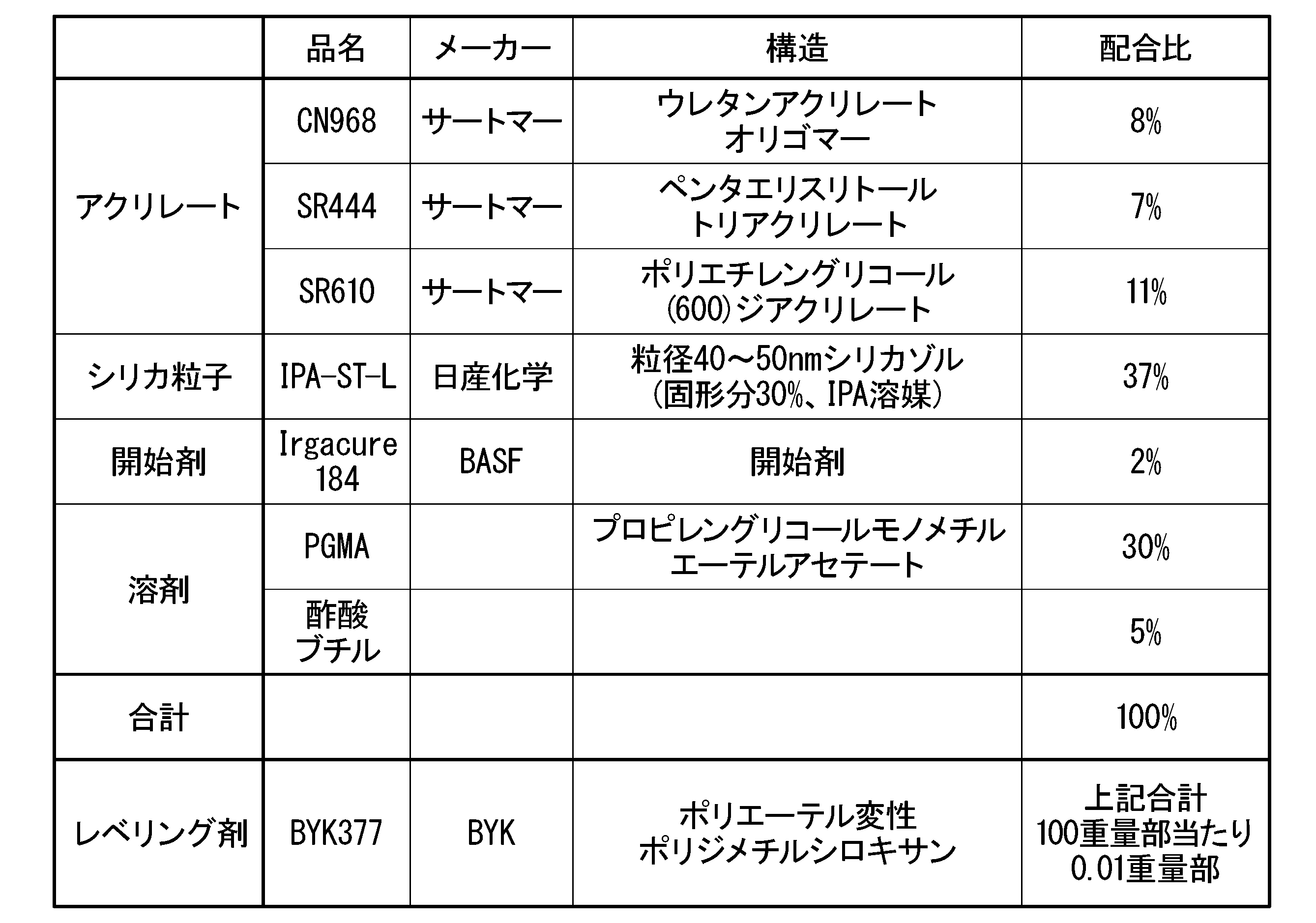
CN968:ポリエステル骨格を有する6官能脂肪族ウレタンアクリレート
Irgacure184:1-ヒドロキシ-シクロヘキシル-フェニル-ケトン SR610: Polyethylene glycol diacrylate, average molecular weight of polyethylene glycol chain 600
CN968: Hex-functional aliphatic urethane acrylate with polyester skeleton Irgacure 184: 1-hydroxy-cyclohexyl-phenyl-ketone
透明基材11として厚さ80μm、長さ3900mのロール状のTACフィルムを用意し、TACフィルム上に表1に示す光硬化性の樹脂組成物をグラビアコーターによって塗布し、光を照射して硬化させ、厚み5μmのハードコート層12を形成した。 <Hard coat layer forming process>
A roll-shaped TAC film having a thickness of 80 μm and a length of 3900 m was prepared as the
製造装置としては、図4に示す製造装置20を用いた。また、ラインスピードは2m/minとした。第1表面処理工程と密着層形成工程と光学機能層形成工程と第2表面処理工程と防汚層形成工程を、製造途中の光学積層体を減圧下の状態に維持したまま連続して行った。 Next, in the roll-to-roll method, the
As the manufacturing apparatus, the
次に、ハードコート層12に対して、グロー放電処理の処理強度を4000W・min/m2にして、グロー放電処理を行った。 <First surface treatment process>
Next, the
グロー放電処理後のハードコート層12上に、圧力1.0Pa以下のチャンバー内で、スパッタリングにより厚み5nmのSiOxからなる密着層13を成膜し、密着層上に厚み15nmのNb2O5膜(高屈折率層)、厚み38nmのSiO2膜(低屈折率層)、厚み30nmのNb2O5膜(高屈折率層)、および厚み102nmのSiO2膜(低屈折率層)からなる光学機能層14(積層体)を成膜した。 <Adhesion layer forming process and optical functional layer forming process>
A
光学機能層14の表面にグロー放電処理を行った。グロー放電は、まずチャンバー内の圧力を2×10⁻⁵Paとした後に、リニアイオンソース内からチャンバー内に800sccmでアルゴンガスを導入し、チャンバー内の圧力を0.4Paとした。グロー放電の電圧、電流値、処理時間によってグロー放電の積算出力を調整した。 <Second surface treatment process>
The surface of the optical
実施例4については、グロー放電処理の積算出力を760W・min/m2とした。
実施例5については、グロー放電処理の積算出力を1086W・min/m2とした。
比較例2については、グロー放電処理の積算出力を3260W・min/m2とした。
比較例4については、グロー放電処理の積算出力を109W・min/m2とした。 For Examples 1 to 3, the integrated output of the glow discharge treatment was set to 326 W · min / m 2 .
In Example 4, the integrated output of the glow discharge treatment was set to 760 W · min / m 2 .
In Example 5, the integrated output of the glow discharge treatment was set to 1086 W · min / m 2 .
For Comparative Example 2, the integrated output of the glow discharge treatment was set to 3260 W · min / m 2 .
For Comparative Example 4, the integrated output of the glow discharge treatment was set to 109 W · min / m 2 .
表面粗さの変化率(%)=((Ra2/Ra1)-1)×100(%)・・・式(1)(式(1)中、Ra1は表面を処理する前の光学機能層の表面粗さ(Ra)を示し、Ra2は表面を処理した後の光学機能層の表面粗さ(Ra)を示す。) Table 2 shows the rate of change in surface roughness represented by the following formula (1).
Rate of change in surface roughness (%) = ((Ra2 / Ra1) -1) x 100 (%) ... In formulas (1) (formula (1), Ra1 is the optical functional layer before surface treatment. The surface roughness (Ra) is shown, and Ra2 shows the surface roughness (Ra) of the optical functional layer after the surface is treated.)
次に、光学機能層14上に、蒸着チャンバー内圧力0.01Pa以下、蒸着温度230℃、ラインスピード2.0m/min、フッ素を有する有機化合物であるパーフルオロポリエーテル基を有するアルコキシシラン化合物(KY-1901、信越化学工業株式会社製)からなる防汚層15を蒸着によって形成した。得られた防汚層15の光学膜厚を表2に示す。
その後、ロール状に巻き取り、実施例1~5、比較例2、比較例4の光学積層体(反射防止フィルム)を得た。 <Anti-fouling layer forming process>
Next, on the optical
Then, the film was wound into a roll to obtain an optical laminate (antireflection film) of Examples 1 to 5, Comparative Example 2, and Comparative Example 4.

実施例1同様にして光学機能層形成工程まで行った後、第2表面処理工程を行わずに防汚層形成工程を行って、光学機能層14上に防汚層15を形成したこと以外は、実施例1同様にして、比較例1の光学積層体(反射防止フィルム)を作製した。 (Comparative Example 1)
Except for the fact that the
実施例1と同様にして光学機能層形成工程まで行った後、ハードコート層12と密着層13と光学機能層14の形成されたTACフィルムを巻き取って製造装置から取り出し、ロールトゥロール方式の塗布装置(コーター)に設置した。その後、大気圧下で、ハードコート層12と密着層13と光学機能層14の形成されたTACフィルムを巻き出し、ラインスピード20m/minで、グラビアコーターを用いて光学機能層14のSiO2膜(低屈折率層)上に防汚剤を塗布した。 (Comparative Example 3)
After performing the optical functional layer forming step in the same manner as in Example 1, the TAC film on which the
光学積層体を巻き取った各ロールの長さ方向中央の位置かつロール幅方向中央の位置から、50mm×50mmの測定サンプルを切り出した。サンプルの表面を原子間力顕微鏡(AFM:Atomic Force Microscope)(商品名SPA400、NanoNaviII;日立株式会社製)を用いて観察し、面積1μm2の範囲における表面粗さRaを測定した。測定はサンプル上の3か所で行い、その平均値を測定値とした。 (Measurement of surface roughness Ra of antifouling layer)
A measurement sample having a size of 50 mm × 50 mm was cut out from the center position in the length direction and the center position in the roll width direction of each roll from which the optical laminate was wound. The surface of the sample was observed using an atomic force microscope (AFM) (trade name: SPA400, NanoNaviII; manufactured by Hitachi, Ltd.), and the surface roughness Ra in an area of 1 μm 2 was measured. The measurement was performed at three places on the sample, and the average value was taken as the measured value.
実施例6~8、比較例5~8は、ハードコートの構成を変えた点が実施例1~5、比較例1~3と異なる。実施例6~8、比較例5~8では、ハードコート層形成工程を行わず、市販品(大日本印刷株式会社製)のフィルムを用いた。ハードコート層は、平均粒子径2μmのフィラーを有するアクリル系樹脂組成物の硬化物である。ハードコート層の膜厚は3μmであった。当該ハードコート層を厚み80μmのTAC(透明基材)上に積層した。そして、実施例6~8、比較例5及び6は、当該ハードコート層に対し、第1表面処理工程、密着層形成工程、光学機能層形成工程、第2表面処理工程及び防汚層形成工程を順に行った。比較例7は、第2表面処理工程を行わなかった。比較例8は、第2表面処理工程を行わず、防汚層を比較例3と同様に、塗布法により形成した。 (Examples 6 to 8, Comparative Examples 5 to 8)
Examples 6 to 8 and Comparative Examples 5 to 8 are different from Examples 1 to 5 and Comparative Examples 1 to 3 in that the hard coat configuration is changed. In Examples 6 to 8 and Comparative Examples 5 to 8, a commercially available film (manufactured by Dai Nippon Printing Co., Ltd.) was used without performing the hard coat layer forming step. The hard coat layer is a cured product of an acrylic resin composition having a filler having an average particle diameter of 2 μm. The film thickness of the hard coat layer was 3 μm. The hard coat layer was laminated on a TAC (transparent substrate) having a thickness of 80 μm. In Examples 6 to 8 and Comparative Examples 5 and 6, the first surface treatment step, the adhesion layer forming step, the optical functional layer forming step, the second surface treatment step and the antifouling layer forming step are applied to the hard coat layer. Was performed in order. In Comparative Example 7, the second surface treatment step was not performed. In Comparative Example 8, the antifouling layer was formed by the coating method in the same manner as in Comparative Example 3 without performing the second surface treatment step.
実施例6、8については、グロー放電処理の積算出力を1086W・min/m2とした。
実施例7については、グロー放電処理の積算出力を1629W・min/m2とした。
比較例5については、グロー放電処理の積算出力を3260W・min/m2とした。
比較例6については、グロー放電処理の積算出力を109W・min/m2とした。 The integrated output of each example of the glow discharge treatment performed in the second surface treatment step is as follows.
For Examples 6 and 8, the integrated output of the glow discharge treatment was set to 1086 W · min / m 2 .
In Example 7, the integrated output of the glow discharge treatment was set to 1629 W · min / m 2 .
For Comparative Example 5, the integrated output of the glow discharge treatment was set to 3260 W · min / m 2 .
For Comparative Example 6, the integrated output of the glow discharge treatment was set to 109 W · min / m 2 .
要素の平均長さの変化率(%)=((RSm2/RSm1)-1)×100(%)・・・式(2)(式(2)中、RSm1は表面を処理する前の光学機能層の要素の平均長さ(RSm)を示し、RSm2は表面を処理した後の光学機能層の要素の平均長さ(RSm)を示す。) Further, in these Examples and Comparative Examples, the rate of change in the average length of the elements represented by the following equation (2) was measured.
Rate of change in average length of elements (%) = ((RSm2 / RSm1) -1) x 100 (%) ... In equations (2) and (2), RSm1 has an optical function before surface treatment. Indicates the average length (RSm) of the elements of the layer, where RSm2 indicates the average length (RSm) of the elements of the optical functional layer after surface treatment.)
光学積層体を巻き取った各ロールの長さ方向中央の位置かつロール幅方向中央の位置から、50mm×50mmの測定サンプルを切り出した。サンプルの表面を原子間力顕微鏡(AFM:Atomic Force Microscope)(商品名SPA400、NanoNaviII;日立株式会社製)を用いて測定し、ハードコート層に含まれる防眩機能を発現するためのフィラーの影響を受けない上面視に於ける直線を3か所選定し、当該3か所の直線に於ける実際の凹凸から面積0.5μm2の範囲における要素の平均長さRSmを平均値として算出した。これらの例の結果を表3にまとめる。 (Measurement of average length RSm of antifouling layer element)
A measurement sample having a size of 50 mm × 50 mm was cut out from the center position in the length direction and the center position in the roll width direction of each roll from which the optical laminate was wound. The surface of the sample was measured using an atomic force microscope (AFM) (trade name: SPA400, NanoNaviII; manufactured by Hitachi, Ltd.), and the effect of the filler contained in the hard coat layer to develop the antiglare function. Three straight lines in the top view that were not affected were selected, and the average length RSm of the elements in the range of 0.5 μm 2 from the actual unevenness in the three straight lines was calculated as the average value. The results of these examples are summarized in Table 3.
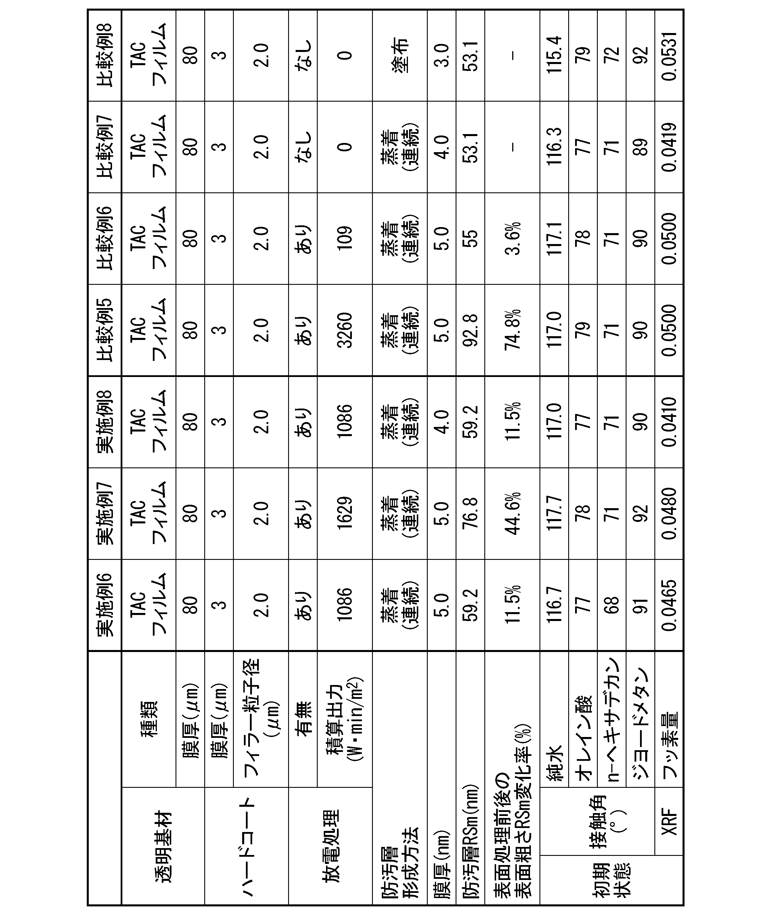
実施例9~12、比較例9~12は、ハードコートの構成を変えた点が実施例1~5、比較例1~3と異なる。実施例9~12、比較例9~12では、ハードコート層形成工程を行わず、市販品(大日本印刷株式会社製)のフィルムを用いた。ハードコート層は、平均粒子径2μmのフィラーを有するアクリル系樹脂組成物の硬化物である。ハードコート層の膜厚は5μmであった。当該ハードコート層を厚み60μmのTAC(透明基材)上に積層した。そして、実施例9~12、比較例9及び10は、当該ハードコート層に対し、第1表面処理工程、密着層形成工程、光学機能層形成工程、第2表面処理工程及び防汚層形成工程を順に行った。比較例11は、第2表面処理工程を行わなかった。比較例12は、第2表面処理工程を行わず、防汚層を比較例3と同様に、塗布法により形成した。 (Examples 9 to 12, Comparative Examples 9 to 12)
Examples 9 to 12 and Comparative Examples 9 to 12 are different from Examples 1 to 5 and Comparative Examples 1 to 3 in that the hard coat configuration is changed. In Examples 9 to 12 and Comparative Examples 9 to 12, a commercially available film (manufactured by Dai Nippon Printing Co., Ltd.) was used without performing the hard coat layer forming step. The hard coat layer is a cured product of an acrylic resin composition having a filler having an average particle diameter of 2 μm. The film thickness of the hard coat layer was 5 μm. The hard coat layer was laminated on a TAC (transparent substrate) having a thickness of 60 μm. In Examples 9 to 12, Comparative Examples 9 and 10, the first surface treatment step, the adhesion layer forming step, the optical functional layer forming step, the second surface treatment step and the antifouling layer forming step are applied to the hard coat layer. Was performed in order. In Comparative Example 11, the second surface treatment step was not performed. In Comparative Example 12, the antifouling layer was formed by the coating method in the same manner as in Comparative Example 3 without performing the second surface treatment step.
実施例9、12については、グロー放電処理の積算出力を1086W・min/m2とした。
実施例10については、グロー放電処理の積算出力を1629W・min/m2とした。
実施例11については、グロー放電処理の積算出力を543W・min/m2とした。
比較例9については、グロー放電処理の積算出力を3260W・min/m2とした。
比較例10については、グロー放電処理の積算出力を109W・min/m2とした。
これらの例の結果を表4にまとめる。 The integrated output of each example of the glow discharge treatment performed in the second surface treatment step is as follows.
For Examples 9 and 12, the integrated output of the glow discharge treatment was set to 1086 W · min / m 2 .
In Example 10, the integrated output of the glow discharge treatment was set to 1629 W · min / m 2 .
In Example 11, the integrated output of the glow discharge treatment was set to 543 W · min / m 2 .
For Comparative Example 9, the integrated output of the glow discharge treatment was set to 3260 W · min / m 2 .
For Comparative Example 10, the integrated output of the glow discharge treatment was set to 109 W · min / m 2 .
The results of these examples are summarized in Table 4.

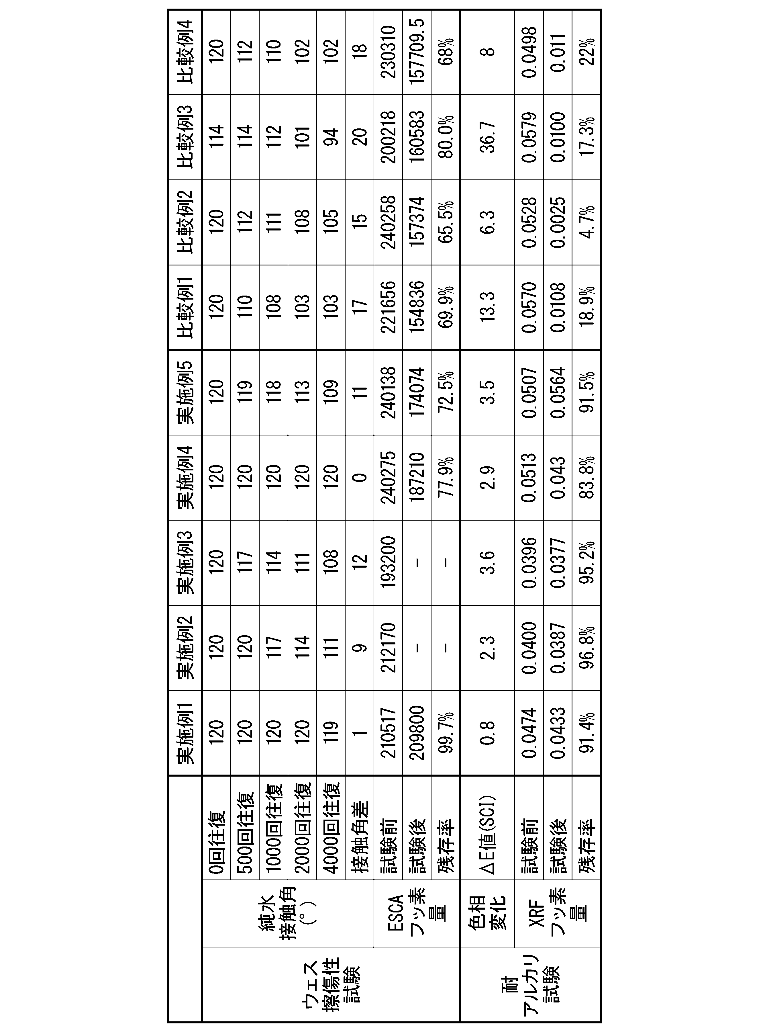
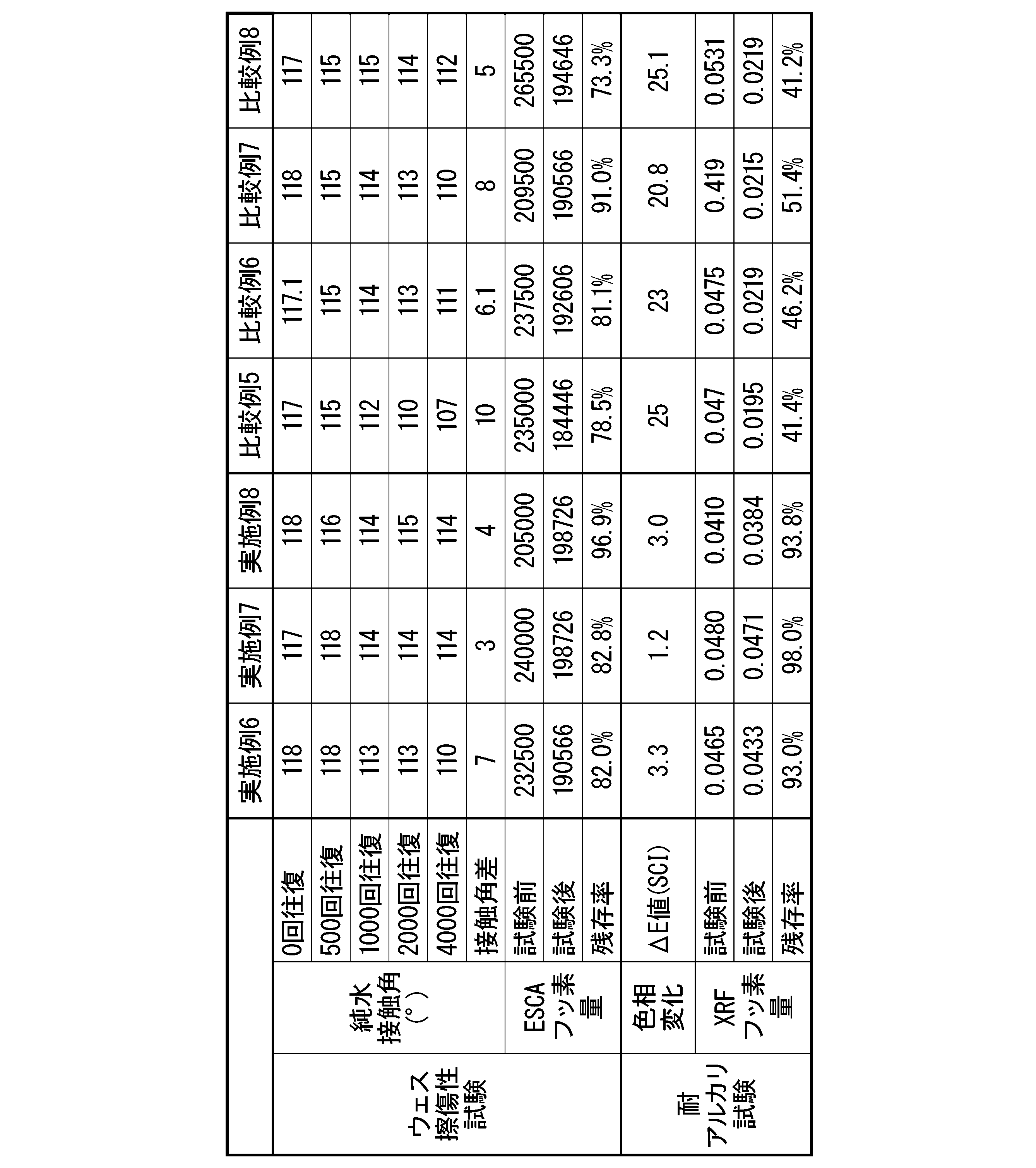


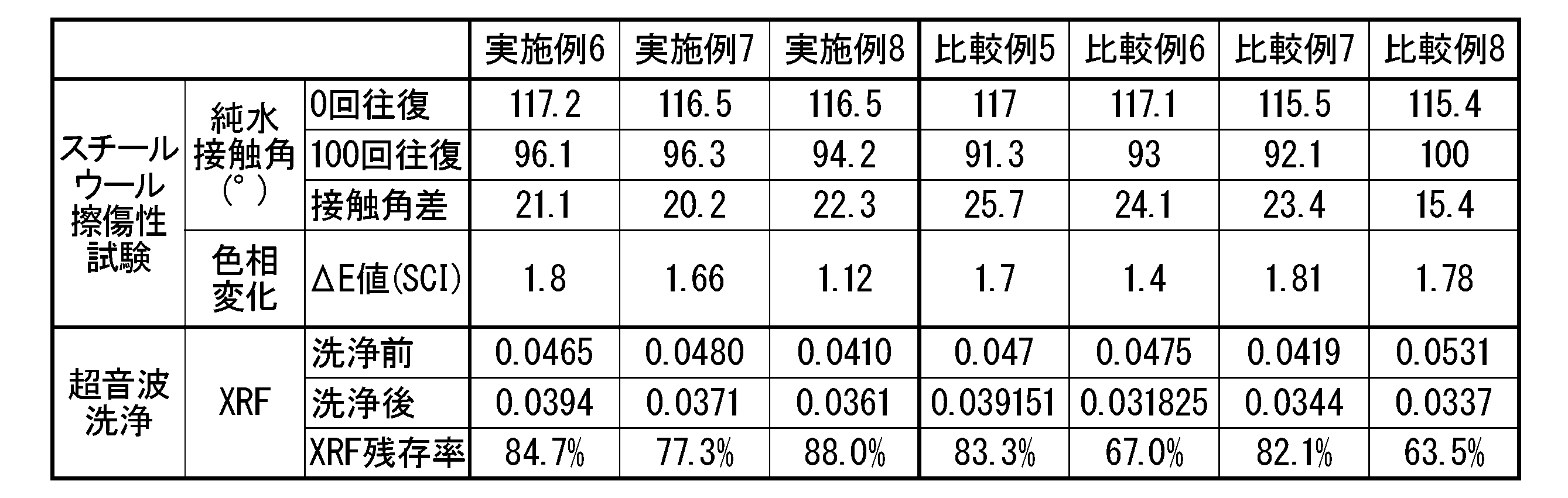
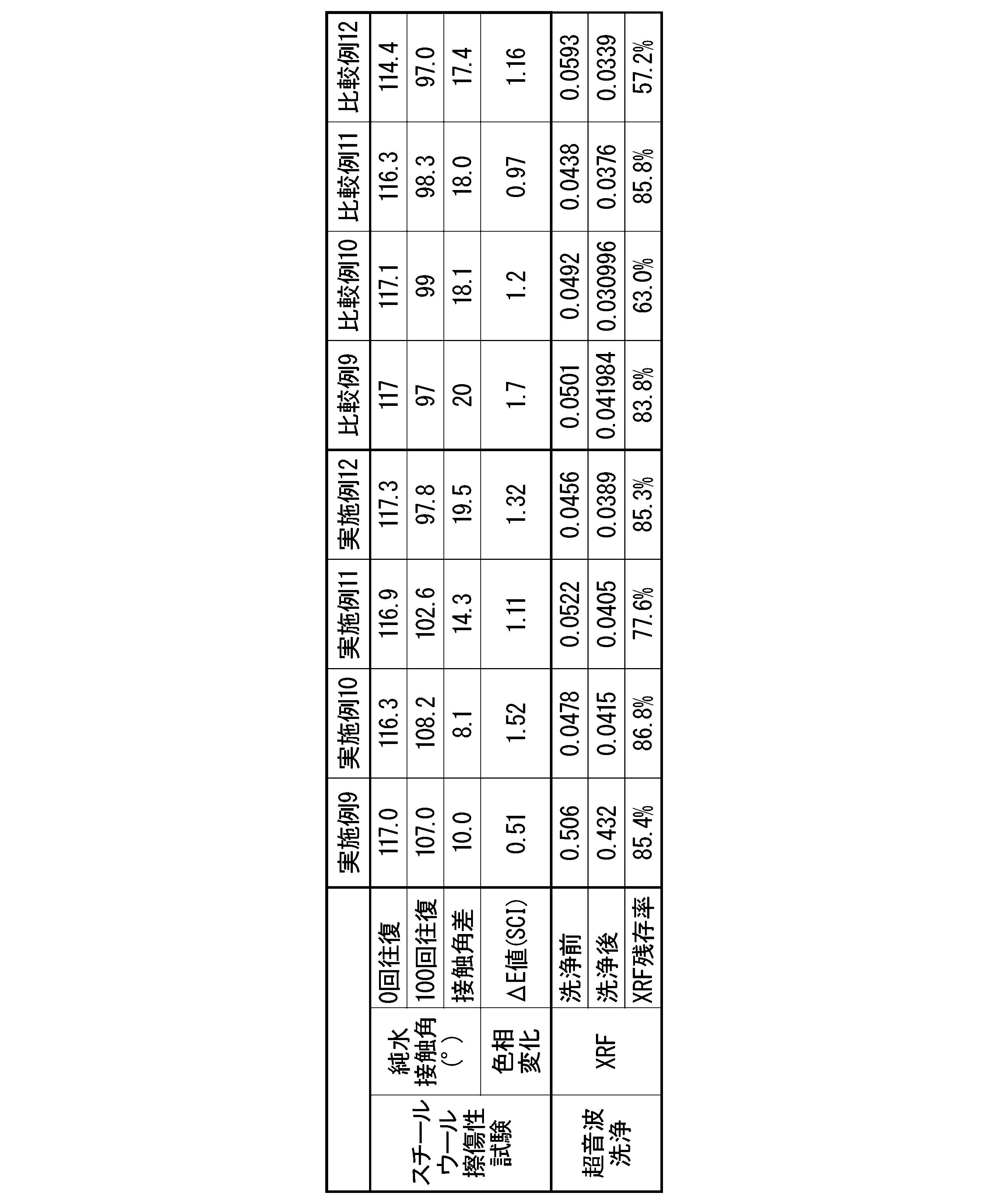
(1-1)純水に対する接触角測定試験
全自動接触角計DM-700(協和界面化学株式会社製)を用い、以下の条件で楕円フィッティング法によって測定した。蒸留水をガラスシリンジに入れて、その先端にステンレス製の針を取り付けて、光学積層体(試験片)に純水を滴下した。
純水の滴下量:2.0μL
測定温度:25℃
純水を滴下して4秒経過後の接触角を、試験片表面の任意の6か所で測定し、その平均値を純水接触角とした。 (1) Contact angle (antifouling property)
(1-1) Contact angle measurement test for pure water Using a fully automatic contact angle meter DM-700 (manufactured by Kyowa Surface Chemistry Co., Ltd.), measurement was performed by the elliptical fitting method under the following conditions. Distilled water was placed in a glass syringe, a stainless steel needle was attached to the tip thereof, and pure water was dropped onto the optical laminate (test piece).
Drop amount of pure water: 2.0 μL
Measurement temperature: 25 ° C
The contact angle after 4 seconds from the dropping of pure water was measured at any 6 points on the surface of the test piece, and the average value was taken as the pure water contact angle.
全自動接触角計DM-700(協和界面化学株式会社製)を用い、以下の条件で楕円フィッティング法によって測定した。上記の各試薬をガラスシリンジに入れて、その先端にステンレス製の針を取り付けて、光学積層体(試験片)に各試薬をそれぞれ滴下した。
各試薬の滴下量:2.0μL
測定温度:25℃
各試薬を滴下して4秒経過後の接触角を、試験片表面の任意の10か所で測定し、その平均値をオレイン酸、n-ヘキサデカン、ジヨードメタンのそれぞれの接触角とした。 (1-2) Contact angle measurement test for oleic acid, n-hexadecane, and diiodomethane (reagent) Measured by the elliptical fitting method using a fully automatic contact angle meter DM-700 (manufactured by Kyowa Surface Chemistry Co., Ltd.) under the following conditions. .. Each of the above reagents was placed in a glass syringe, a stainless steel needle was attached to the tip thereof, and each reagent was dropped onto the optical laminate (test piece).
Drop amount of each reagent: 2.0 μL
Measurement temperature: 25 ° C
The contact angle after 4 seconds after dropping each reagent was measured at any 10 points on the surface of the test piece, and the average value was taken as the contact angle of oleic acid, n-hexadecane, and diiodomethane.
光学積層体(試験片)のフッ素量(cps:単位時間当たりのカウント数)を測定した(洗浄前フッ素量(初期状態のフッ素量))。 (2) Fluorine amount measurement test The fluorine amount (cps: count number per unit time) of the optical laminate (test piece) was measured (fluorine amount before cleaning (fluorine amount in the initial state)).
光学積層体(試験片)の光学特性を測定した(処理前サンプル)。
次に、濃度0.1mol/Lの水酸化ナトリウム水溶液(試薬)を調整した。
そして、光学積層体(試験片)に、内径38mmの円筒状部材を密着させ、その中に試薬を滴下し、ガラス板で上面開口に蓋をした。そして、液温55℃に保って4時間静置後、各試験片を蒸留水で洗浄し、処理後サンプルを得た。 (3) Alkali resistance test The optical characteristics of the optical laminate (test piece) were measured (sample before treatment).
Next, a sodium hydroxide aqueous solution (reagent) having a concentration of 0.1 mol / L was prepared.
Then, a cylindrical member having an inner diameter of 38 mm was brought into close contact with the optical laminate (test piece), a reagent was dropped therein, and the upper surface opening was covered with a glass plate. Then, after keeping the liquid temperature at 55 ° C. and allowing it to stand for 4 hours, each test piece was washed with distilled water to obtain a treated sample.
上述した処理前サンプルおよび処理後サンプルの裏面を透明テープで黒色アクリル板に貼着し、裏面反射を無くした。そして、光学特性を測定した。
光学測定には、積分球分光測色計(SP-64:X-rite株式会社製)を使用した。設定は、D65光源、10°とし、処理前サンプルおよび処理後サンプルのSCI(Specular Component Include、正反射光を考慮に入れた反射色の測定方法)による上記式(2)で示されるL*a*b*(CIE1976に準拠)値の変化量であるΔE値を算出した。
(3-2)アルカリ溶液によるフッ素残留量測定試験
上述した(2)の試験と同様にして、ESCA又はXRFを用いてアルカリ溶液による処理後サンプルのフッ素量(cps)を測定し、処理後サンプルのフッ素の残存率(%)を算出した。 (3-1) Optical characteristic measurement (hue change)
The back surfaces of the pre-treatment sample and the post-treatment sample described above were attached to a black acrylic plate with a transparent tape to eliminate backside reflection. Then, the optical characteristics were measured.
An integrating sphere spectrophotometer (SP-64: manufactured by X-Rite Co., Ltd.) was used for the optical measurement. The setting is a D65 light source, 10 °, and L * a represented by the above equation (2) by SCI (Specular Component Industry, a method for measuring the reflected color in consideration of specular reflected light) of the pre-processed sample and the post-processed sample. The ΔE value, which is the amount of change in the * b * (based on CIE1976) value, was calculated.
(3-2) Fluorine Residual Amount Measurement Test with Alkaline Solution In the same manner as the test in (2) above, the fluorine amount (cps) of the sample after treatment with the alkaline solution was measured using ESCA or XRF, and the treated sample. Fluorine residual rate (%) was calculated.
JIS L0849に準拠した摩擦試験機I形を用いて、光学積層体(試験片)の表面に沿って、摩擦体を水平往復運動させ、試験片を得た。
摩擦体としてスチールウール(ボンスター株式会社製 #0000番)を用いた。試験設定は、荷重1000g/cm2、ストローク75mm、速度7mm/sとした。表に摩擦体の水平往復回数を示す。 (4) Scratch resistance test using steel wool Using a friction tester type I compliant with JIS L0849, the friction body is horizontally reciprocated along the surface of the optical laminate (test piece) to obtain a test piece. rice field.
Steel wool (# 0000 manufactured by Bonstar Co., Ltd.) was used as the friction body. The test settings were a load of 1000 g / cm 2 , a stroke of 75 mm, and a speed of 7 mm / s. The table shows the number of horizontal round trips of the friction body.
上述した(1-1)の試験と同様にして、摩擦後の試験片の接触角を測定し、摩擦前と500回水平往復運動(実施例6~12、比較例5~12は100回水平往復運動)させた摩擦後の試験片の接触角差を求めた。試験は摩擦後30分以内に実施した。
(4-2)光学特性測定(色相変化)
上述した(3-1)の試験と同様にして、摩擦前と500回水平往復運動(実施例6~12、比較例5~12は100回水平往復運動)させた摩擦後の試験片のSCIによるΔL*a*b*値の変化量であるΔE値を算出した。
また、上述した(3-1)の試験と同様にして、摩擦前と500回水平往復運動(実施例6~12、比較例5~12は100回水平往復運動)させた摩擦後の試験片のSCE(Specular Component Exclude、正反射光を考慮に入れない反射色の測定法)による上記式(3)で示されるL*a*b*値の変化量であるΔE値を算出した。 (4-1) Contact angle In the same manner as in the test of (1-1) described above, the contact angle of the test piece after friction was measured, and the horizontal reciprocating motion before friction and 500 times (Examples 6 to 12, Comparative Example). The contact angle difference of the test piece after rubbing after being subjected to horizontal reciprocating motion 100 times for 5 to 12 was determined. The test was performed within 30 minutes after rubbing.
(4-2) Optical characteristic measurement (hue change)
Similar to the above-mentioned test (3-1), the SCI of the test piece before rubbing and after rubbing 500 times of horizontal reciprocating motion (Examples 6 to 12 and Comparative Examples 5 to 12 are 100 times horizontal reciprocating motion). The ΔE value, which is the amount of change in the ΔL * a * b * value according to the above, was calculated.
Further, in the same manner as in the above-mentioned test (3-1), the test piece before rubbing and after rubbing 500 times of horizontal reciprocating motion (Examples 6 to 12 and Comparative Examples 5 to 12 are 100 times horizontal reciprocating motion). The ΔE value, which is the amount of change in the L * a * b * value represented by the above equation (3), was calculated by SCE (Specular Component Exclude, a method for measuring the reflected color that does not take into account the specular reflected light).
摩擦体としてウェス(不織布ワイパー)(ベンコットリントフリーCT-8、旭化成工業株式会社製)を用いたほかは、スチールウールを用いた擦傷性試験と同様にして擦傷性試験を実施した。試験設定は、荷重250g/cm2、ストローク25mm、速度50mm/sとした。表に摩擦体の水平往復運動回数を示す。
(5-1)接触角
上述した(1-1)の試験と同様にして、摩擦後の試験片の接触角を測定し、摩擦前と4000回水平往復運動させた摩擦後の試験片の接触角差を求めた。試験は摩擦後30分以内に実施した。 (5) Scratch resistance test using waste cloth (non-woven fabric wiper) Scratch resistance test using steel wool other than using waste cloth (non-woven fabric wiper) (Bencot Lint Free CT-8, manufactured by Asahi Kasei Kogyo Co., Ltd.) as a friction body. The scratch resistance test was carried out in the same manner as above. The test settings were a load of 250 g / cm 2 , a stroke of 25 mm, and a speed of 50 mm / s. The table shows the number of horizontal reciprocating motions of the friction body.
(5-1) Contact angle In the same manner as in the test of (1-1) described above, the contact angle of the test piece after friction was measured, and the contact of the test piece before friction and after friction after being horizontally reciprocated 4000 times. The angle difference was calculated. The test was performed within 30 minutes after rubbing.
上述した(2)の試験と同様にして、ESCAを用いてウェスを用いた水平往復運動を4000回行った後の処理後サンプルのフッ素量(cps)を測定し、処理後サンプルのフッ素の残存率(%)を算出した。 (5-2) Fluorine Residual Amount Measurement Test Similar to the test of (2) described above, the fluorine amount (cps) of the treated sample after performing horizontal reciprocating motion using a waste cloth 4000 times using ESCA is measured. The measurement was performed, and the residual rate (%) of fluorine in the treated sample was calculated.
フッ素系溶剤(フロリナートFC-3283:スリーエムジャパン株式会社製)を容器に入れ、光学積層体(試験片)を浸漬させて、超音波洗浄機(USK-5R、アズワン社製)を用い、40KHz、240Wで10分間超音波を印加した。その後、上記フッ素系溶剤を用いて試験片を洗い流した。そしてXRFを用いて超音波洗浄後サンプルのフッ素量(cps)を測定し、洗浄後サンプルのフッ素の残存率(%)を算出した。 (6) Ultrasonic cleaning test A fluorine-based solvent (Florinate FC-3283: manufactured by 3M Japan Co., Ltd.) is placed in a container, and an optical laminate (test piece) is immersed in the ultrasonic cleaning machine (USK-5R, AS ONE). ) Was used, and ultrasonic waves were applied at 40 KHz and 240 W for 10 minutes. Then, the test piece was washed away with the above-mentioned fluorine-based solvent. Then, the amount of fluorine (cps) of the sample after ultrasonic cleaning was measured using XRF, and the residual rate (%) of fluorine of the sample after cleaning was calculated.
また、実施例1~5の光学積層体は、比較例1および2と比較して、ウェス(不織布ワイパー)を用いた擦傷性試験での接触角差が14以下と小さく、フッ素の残留率が高かった。
実施例1~5の光学積層体は、比較例1および2と比較して、耐アルカリ性試験での色相変化が小さく、フッ素の残留率が高かった。 As shown in Tables 2 to 4, a surface treatment step of treating the surface of the optical
Further, the optical laminates of Examples 1 to 5 have a smaller contact angle difference of 14 or less in the scratch resistance test using a waste cloth (nonwoven fabric wiper) and a residual rate of fluorine as compared with Comparative Examples 1 and 2. it was high.
The optical laminates of Examples 1 to 5 had a smaller hue change in the alkali resistance test and a higher residual rate of fluorine as compared with Comparative Examples 1 and 2.
11…透明基材
12…ハードコート層
13…密着層
14…光学機能層
14a…高屈折率層
14b…低屈折率層
15…防汚層
20…製造装置
1…スパッタリング装置
2A、2B…前処理装置
3…蒸着装置
4…ロール巻き出し装置
5…ロール巻き取り装置
20…製造装置
21…真空ポンプ
22…ガイドロール
23…巻き出しロール
24…巻き取りロール
25…成膜ロール
26…キャンロール
31、32、33、34、35…チャンバー
41…成膜部
42…プラズマ放電装置
43…蒸着源
53…加熱装置 10, 101, 102 ...
Claims (12)
- プラスチックフィルムと、密着層と、光学機能層と、防汚層とが順に積層されてなる光学積層体の製造方法であって、
密着層を形成する密着層形成工程と、
光学機能層を形成する光学機能層形成工程と、
下記式(1)で表される表面粗さの変化率が1~25%、または、下記式(2)で表される要素の平均長さの変化率が7~65%となるように、前記光学機能層の表面を処理する表面処理工程と、
表面処理された前記光学機能層上に防汚層を形成する防汚層形成工程と、を含む光学積層体の製造方法。
表面粗さの変化率(%)=((Ra2/Ra1)-1)×100(%)・・・式(1)
(式(1)中、Ra1は表面を処理する前の光学機能層の表面粗さ(Ra)を示し、Ra2は表面を処理した後の光学機能層の表面粗さ(Ra)を示す。)
要素の平均長さの変化率(%)=((RSm2/RSm1)-1)×100(%)・・・式(2)
(式(2)中、RSm1は表面を処理する前の光学機能層の要素の平均長さ(RSm)を示し、RSm2は表面を処理した後の光学機能層の要素の平均長さ(RSm)を示す。) A method for manufacturing an optical laminate in which a plastic film, an adhesive layer, an optical functional layer, and an antifouling layer are laminated in this order.
The adhesion layer forming process for forming the adhesion layer and
The process of forming the optical functional layer and the process of forming the optical functional layer,
The rate of change in surface roughness represented by the following formula (1) is 1 to 25%, or the rate of change in the average length of the elements represented by the following formula (2) is 7 to 65%. A surface treatment step for treating the surface of the optical functional layer and
A method for producing an optical laminate, comprising a step of forming an antifouling layer on the surface-treated optical functional layer.
Rate of change in surface roughness (%) = ((Ra2 / Ra1) -1) x 100 (%) ... Equation (1)
(In the formula (1), Ra1 indicates the surface roughness (Ra) of the optical functional layer before the surface is treated, and Ra2 indicates the surface roughness (Ra) of the optical functional layer after the surface is treated.)
Rate of change in average length of elements (%) = ((RSm2 / RSm1) -1) x 100 (%) ... Equation (2)
(In the formula (2), RSm1 indicates the average length (RSm) of the elements of the optical functional layer before the surface is treated, and RSm2 is the average length (RSm) of the elements of the optical functional layer after the surface is treated. Shows.) - プラスチックフィルムと、密着層と、光学機能層と、防汚層とが順に積層されてなる光学積層体の製造方法であって、
密着層を形成する密着層形成工程と、
光学機能層を形成する光学機能層形成工程と、
前記光学機能層の表面をグロー放電処理する表面処理工程と、
表面処理された前記光学機能層上に防汚層を形成する防汚層形成工程と、を含み、
前記グロー放電処理の積算出力は、130W・min/m2以上2000W・min/m2以下である、光学積層体の製造方法。 A method for manufacturing an optical laminate in which a plastic film, an adhesive layer, an optical functional layer, and an antifouling layer are laminated in this order.
The adhesion layer forming process for forming the adhesion layer and
The process of forming the optical functional layer and the process of forming the optical functional layer,
A surface treatment step of glow-discharging the surface of the optical functional layer and
Including an antifouling layer forming step of forming an antifouling layer on the surface-treated optical functional layer.
A method for manufacturing an optical laminate, wherein the integrated output of the glow discharge treatment is 130 W · min / m 2 or more and 2000 W · min / m 2 or less. - 前記密着層形成工程および前記光学機能層形成工程において、スパッタリングによって前記密着層および前記光学機能層を形成する、請求項1または請求項2に記載の光学積層体の製造方法。 The method for manufacturing an optical laminate according to claim 1 or 2, wherein in the adhesion layer forming step and the optical functional layer forming step, the adhesion layer and the optical functional layer are formed by sputtering.
- 前記防汚層形成工程において、真空蒸着によって前記防汚層を形成する、請求項1~請求項3のいずれか一項に記載の光学積層体の製造方法。 The method for manufacturing an optical laminate according to any one of claims 1 to 3, wherein the antifouling layer is formed by vacuum vapor deposition in the antifouling layer forming step.
- 前記密着層形成工程および前記光学機能層形成工程と前記表面処理工程と前記防汚層形成工程とを、減圧下で連続して行う、請求項1~請求項4のいずれか一項に記載の光学積層体の製造方法。 The aspect according to any one of claims 1 to 4, wherein the adhesion layer forming step, the optical functional layer forming step, the surface treatment step, and the antifouling layer forming step are continuously performed under reduced pressure. A method for manufacturing an optical laminate.
- 前記密着層形成工程の前に、ハードコート層を形成するハードコート層形成工程を有する、請求項1~請求項5のいずれか一項に記載の光学積層体の製造方法。 The method for manufacturing an optical laminate according to any one of claims 1 to 5, further comprising a hard coat layer forming step of forming a hard coat layer before the close contact layer forming step.
- 前記光学機能層は、反射防止層及び選択反射層から選ばれるいずれか1種を含む、請求項1~請求項6のいずれか一項に記載の光学積層体の製造方法。 The method for manufacturing an optical laminate according to any one of claims 1 to 6, wherein the optical functional layer includes any one selected from an antireflection layer and a selective reflection layer.
- 前記光学機能層が、低屈折率層を備える、請求項1~請求項7のいずれか一項に記載の光学積層体の製造方法。 The method for manufacturing an optical laminate according to any one of claims 1 to 7, wherein the optical functional layer includes a low refractive index layer.
- 前記光学機能層形成工程が、低屈折率層と高屈折率層とを交互に積層して積層体を形成する工程である、請求項1~請求項7のいずれか一項に記載の光学積層体の製造方法。 The optical lamination according to any one of claims 1 to 7, wherein the optical functional layer forming step is a step of alternately laminating low refractive index layers and high refractive index layers to form a laminated body. How to make a body.
- 前記表面処理工程において、前記低屈折率層の表面を処理する、請求項8または請求項9に記載の光学積層体の製造方法。 The method for producing an optical laminate according to claim 8 or 9, wherein the surface of the low refractive index layer is treated in the surface treatment step.
- 前記低屈折率層が、金属の酸化物を含む、請求項8~請求項10のいずれか一項に記載の光学積層体の製造方法。 The method for producing an optical laminate according to any one of claims 8 to 10, wherein the low refractive index layer contains a metal oxide.
- 前記密着層が、金属又は金属酸化物を含む、請求項1~11のいずれか一項に記載の光学積層体の製造方法。 The method for producing an optical laminate according to any one of claims 1 to 11, wherein the adhesion layer contains a metal or a metal oxide.
Priority Applications (4)
| Application Number | Priority Date | Filing Date | Title |
|---|---|---|---|
| KR1020227042784A KR20230007487A (en) | 2020-07-17 | 2021-07-16 | Manufacturing method of optical laminate |
| CN202180048162.0A CN115812032A (en) | 2020-07-17 | 2021-07-16 | Method for manufacturing optical laminate |
| US17/998,449 US20230191732A1 (en) | 2020-07-17 | 2021-07-16 | Method for producing optical multilayer body |
| EP21841832.5A EP4183573A1 (en) | 2020-07-17 | 2021-07-16 | Method for producing optical multilayer body |
Applications Claiming Priority (4)
| Application Number | Priority Date | Filing Date | Title |
|---|---|---|---|
| JP2020-123317 | 2020-07-17 | ||
| JP2020123317 | 2020-07-17 | ||
| JP2021-032929 | 2021-03-02 | ||
| JP2021032929A JP7089610B2 (en) | 2020-03-04 | 2021-03-02 | Manufacturing method of optical laminate |
Publications (1)
| Publication Number | Publication Date |
|---|---|
| WO2022014701A1 true WO2022014701A1 (en) | 2022-01-20 |
Family
ID=79555645
Family Applications (1)
| Application Number | Title | Priority Date | Filing Date |
|---|---|---|---|
| PCT/JP2021/026794 WO2022014701A1 (en) | 2020-07-17 | 2021-07-16 | Method for producing optical multilyer body |
Country Status (5)
| Country | Link |
|---|---|
| US (1) | US20230191732A1 (en) |
| EP (1) | EP4183573A1 (en) |
| KR (1) | KR20230007487A (en) |
| CN (1) | CN115812032A (en) |
| WO (1) | WO2022014701A1 (en) |
Cited By (2)
| Publication number | Priority date | Publication date | Assignee | Title |
|---|---|---|---|---|
| JP7134373B1 (en) | 2022-03-10 | 2022-09-09 | デクセリアルズ株式会社 | OPTICAL LAMINATE, ARTICLE AND IMAGE DISPLAY DEVICE |
| JP7241949B1 (en) | 2022-03-10 | 2023-03-17 | デクセリアルズ株式会社 | OPTICAL LAMINATE, ARTICLE AND IMAGE DISPLAY DEVICE |
Citations (16)
| Publication number | Priority date | Publication date | Assignee | Title |
|---|---|---|---|---|
| JPH0242970B2 (en) | 1985-04-02 | 1990-09-26 | ||
| JP2000308846A (en) * | 1999-04-26 | 2000-11-07 | Toppan Printing Co Ltd | Method for formation of antifouling layer |
| JP2005301208A (en) | 2004-03-17 | 2005-10-27 | Seiko Epson Corp | Method for manufacturing stain proof optical article |
| JP2006175438A (en) | 2005-12-22 | 2006-07-06 | Toppan Printing Co Ltd | Forming method of stain-proofing layer |
| JP2008062460A (en) * | 2006-09-06 | 2008-03-21 | Konica Minolta Holdings Inc | Optical film and image display element using it |
| JP2010191144A (en) * | 2009-02-18 | 2010-09-02 | Toppan Printing Co Ltd | Antireflection film |
| JP2011013654A (en) * | 2008-10-23 | 2011-01-20 | Seiko Epson Corp | Multilayer antireflection layer and method of producing the same, and plastic lens |
| WO2014129333A1 (en) * | 2013-02-22 | 2014-08-28 | 旭硝子株式会社 | Optical component |
| CN105835465A (en) * | 2015-01-13 | 2016-08-10 | 南昌欧菲光学技术有限公司 | Antireflective anti-fingerprint laminate and manufacturing method thereof |
| WO2018193742A1 (en) * | 2017-04-20 | 2018-10-25 | 信越化学工業株式会社 | Antireflective member and method of manufacture therefor |
| WO2019064969A1 (en) * | 2017-09-28 | 2019-04-04 | 日東電工株式会社 | Anti-reflection film, method for producing same, and polarizing plate with anti-reflection layer |
| WO2019078313A1 (en) | 2017-10-19 | 2019-04-25 | Agc株式会社 | Transparent substrate laminated body and method for producing same |
| WO2020027037A1 (en) * | 2018-07-31 | 2020-02-06 | 日本電産株式会社 | Coating method, optical component, and lens assembly |
| JP2020519557A (en) * | 2017-05-08 | 2020-07-02 | コーニング インコーポレイテッド | Glasses, glass ceramics and ceramic articles having durable and slippery anti-fingerprint coatings on optical and scratch resistant coatings and methods of making the same |
| JP2020123317A (en) | 2019-01-25 | 2020-08-13 | ベイジン バイドゥ ネットコム サイエンス アンド テクノロジー カンパニー リミテッド | Method and device for controlling travel of vehicle |
| JP2021032929A (en) | 2019-08-16 | 2021-03-01 | 株式会社電子技販 | Light-emitting display device |
Family Cites Families (1)
| Publication number | Priority date | Publication date | Assignee | Title |
|---|---|---|---|---|
| JP6542970B2 (en) | 2018-10-10 | 2019-07-10 | デクセリアルズ株式会社 | Method of manufacturing antireflective film |
-
2021
- 2021-07-16 KR KR1020227042784A patent/KR20230007487A/en not_active Application Discontinuation
- 2021-07-16 WO PCT/JP2021/026794 patent/WO2022014701A1/en active Application Filing
- 2021-07-16 US US17/998,449 patent/US20230191732A1/en active Pending
- 2021-07-16 CN CN202180048162.0A patent/CN115812032A/en active Pending
- 2021-07-16 EP EP21841832.5A patent/EP4183573A1/en active Pending
Patent Citations (16)
| Publication number | Priority date | Publication date | Assignee | Title |
|---|---|---|---|---|
| JPH0242970B2 (en) | 1985-04-02 | 1990-09-26 | ||
| JP2000308846A (en) * | 1999-04-26 | 2000-11-07 | Toppan Printing Co Ltd | Method for formation of antifouling layer |
| JP2005301208A (en) | 2004-03-17 | 2005-10-27 | Seiko Epson Corp | Method for manufacturing stain proof optical article |
| JP2006175438A (en) | 2005-12-22 | 2006-07-06 | Toppan Printing Co Ltd | Forming method of stain-proofing layer |
| JP2008062460A (en) * | 2006-09-06 | 2008-03-21 | Konica Minolta Holdings Inc | Optical film and image display element using it |
| JP2011013654A (en) * | 2008-10-23 | 2011-01-20 | Seiko Epson Corp | Multilayer antireflection layer and method of producing the same, and plastic lens |
| JP2010191144A (en) * | 2009-02-18 | 2010-09-02 | Toppan Printing Co Ltd | Antireflection film |
| WO2014129333A1 (en) * | 2013-02-22 | 2014-08-28 | 旭硝子株式会社 | Optical component |
| CN105835465A (en) * | 2015-01-13 | 2016-08-10 | 南昌欧菲光学技术有限公司 | Antireflective anti-fingerprint laminate and manufacturing method thereof |
| WO2018193742A1 (en) * | 2017-04-20 | 2018-10-25 | 信越化学工業株式会社 | Antireflective member and method of manufacture therefor |
| JP2020519557A (en) * | 2017-05-08 | 2020-07-02 | コーニング インコーポレイテッド | Glasses, glass ceramics and ceramic articles having durable and slippery anti-fingerprint coatings on optical and scratch resistant coatings and methods of making the same |
| WO2019064969A1 (en) * | 2017-09-28 | 2019-04-04 | 日東電工株式会社 | Anti-reflection film, method for producing same, and polarizing plate with anti-reflection layer |
| WO2019078313A1 (en) | 2017-10-19 | 2019-04-25 | Agc株式会社 | Transparent substrate laminated body and method for producing same |
| WO2020027037A1 (en) * | 2018-07-31 | 2020-02-06 | 日本電産株式会社 | Coating method, optical component, and lens assembly |
| JP2020123317A (en) | 2019-01-25 | 2020-08-13 | ベイジン バイドゥ ネットコム サイエンス アンド テクノロジー カンパニー リミテッド | Method and device for controlling travel of vehicle |
| JP2021032929A (en) | 2019-08-16 | 2021-03-01 | 株式会社電子技販 | Light-emitting display device |
Cited By (5)
| Publication number | Priority date | Publication date | Assignee | Title |
|---|---|---|---|---|
| JP7134373B1 (en) | 2022-03-10 | 2022-09-09 | デクセリアルズ株式会社 | OPTICAL LAMINATE, ARTICLE AND IMAGE DISPLAY DEVICE |
| JP7241949B1 (en) | 2022-03-10 | 2023-03-17 | デクセリアルズ株式会社 | OPTICAL LAMINATE, ARTICLE AND IMAGE DISPLAY DEVICE |
| WO2023171567A1 (en) * | 2022-03-10 | 2023-09-14 | デクセリアルズ株式会社 | Optical laminate, article, and image display device |
| JP2023132237A (en) * | 2022-03-10 | 2023-09-22 | デクセリアルズ株式会社 | Optical laminate, article and image display device |
| JP2023133067A (en) * | 2022-03-10 | 2023-09-22 | デクセリアルズ株式会社 | Optical laminate, article and picture display unit |
Also Published As
| Publication number | Publication date |
|---|---|
| US20230191732A1 (en) | 2023-06-22 |
| CN115812032A (en) | 2023-03-17 |
| EP4183573A1 (en) | 2023-05-24 |
| KR20230007487A (en) | 2023-01-12 |
Similar Documents
| Publication | Publication Date | Title |
|---|---|---|
| WO2021177350A1 (en) | Optical laminate, article, and method for producing optical laminate | |
| JP7101297B2 (en) | Manufacturing method of optical laminate, article, optical laminate | |
| JP7147095B2 (en) | Method for manufacturing optical laminate | |
| WO2022014701A1 (en) | Method for producing optical multilyer body | |
| JP7273238B2 (en) | Method for manufacturing optical laminate | |
| JP7089609B2 (en) | Manufacturing method of optical laminate, article, optical laminate | |
| JP7089610B2 (en) | Manufacturing method of optical laminate | |
| WO2022014696A1 (en) | Optical laminate, article, and method for producing optical laminate | |
| JP7303954B2 (en) | Method for manufacturing optical laminate | |
| JP7248830B2 (en) | Method for manufacturing optical laminate | |
| TW202216458A (en) | Method for manufacturing optical laminate |
Legal Events
| Date | Code | Title | Description |
|---|---|---|---|
| 121 | Ep: the epo has been informed by wipo that ep was designated in this application |
Ref document number: 21841832 Country of ref document: EP Kind code of ref document: A1 |
|
| WWE | Wipo information: entry into national phase |
Ref document number: 202217064221 Country of ref document: IN |
|
| ENP | Entry into the national phase |
Ref document number: 20227042784 Country of ref document: KR Kind code of ref document: A |
|
| NENP | Non-entry into the national phase |
Ref country code: DE |
|
| ENP | Entry into the national phase |
Ref document number: 2021841832 Country of ref document: EP Effective date: 20230217 |