JP2022012271A - Organic EL display device - Google Patents
Organic EL display device Download PDFInfo
- Publication number
- JP2022012271A JP2022012271A JP2020113985A JP2020113985A JP2022012271A JP 2022012271 A JP2022012271 A JP 2022012271A JP 2020113985 A JP2020113985 A JP 2020113985A JP 2020113985 A JP2020113985 A JP 2020113985A JP 2022012271 A JP2022012271 A JP 2022012271A
- Authority
- JP
- Japan
- Prior art keywords
- organic
- pigment
- color filter
- display device
- layer
- Prior art date
- Legal status (The legal status is an assumption and is not a legal conclusion. Google has not performed a legal analysis and makes no representation as to the accuracy of the status listed.)
- Granted
Links
Images

Landscapes
- Optical Filters (AREA)
- Electroluminescent Light Sources (AREA)
- Devices For Indicating Variable Information By Combining Individual Elements (AREA)
Abstract
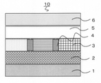
【課題】混色の問題が無く、且つブラックマトリクスを備えたカラーフィルタを形成した場合より高い輝度を持つ有機EL表示装置を提供する。【解決手段】駆動回路が形成された半導体基板1上に、少なくとも、有機EL素子2とカラーフィルタ3がこの順に備えられた有機EL表示装置において、カラーフィルタの各着色画素の間には各着色画素を区画する樹脂パターン4が備えられており、前記樹脂パターンの幅方向の380nm以上780nm以下の波長領域における最大透過率が20%以下であり、前記樹脂パターンの表面の380nm以上780nm以下の波長領域における最小反射率が15%以上である事を特徴とする有機EL表示装置10。【選択図】図1Kind Code: A1 To provide an organic EL display device free from the problem of color mixture and having higher luminance than when a color filter having a black matrix is formed. Kind Code: A1 In an organic EL display device in which at least an organic EL element 2 and a color filter 3 are provided in this order on a semiconductor substrate 1 on which a drive circuit is formed, each colored pixel is provided between each colored pixel of the color filter. A resin pattern 4 for partitioning pixels is provided, and the maximum transmittance in the wavelength region of 380 nm or more and 780 nm or less in the width direction of the resin pattern is 20% or less, and the wavelength of 380 nm or more and 780 nm or less of the surface of the resin pattern. An organic EL display device 10 characterized by having a minimum reflectance of 15% or more in a region. [Selection drawing] Fig. 1
Description
本発明は、有機エレクトロルミネッセンス(有機Electro-Luminescence、以下、有機ELと称する。)表示装置に関する。更に詳しくは、混色が無く、輝度が高い有機EL表示装置に関する。 The present invention relates to an organic electroluminescence (organic Electro-Luminescence, hereinafter referred to as organic EL) display device. More specifically, the present invention relates to an organic EL display device having no color mixing and high brightness.
近年、携帯電話機や携帯情報端末などの電子機器において、現在の主流である液晶表示装置では困難であった更なる薄型・軽量化や曲面表示の要求に対応するため、自発光素子である有機ELを用いた表示装置の開発・量産化が進んでいる。その中でも、薄型・軽量化の特徴を活かすため、ヘッドマウントディスプレイ、電子ビューファインダなどの高精細かつ0.5インチ程度の小型ディスプレイ(以下、マイクロディスプレイと称する。)への応用が期待されている。 In recent years, in electronic devices such as mobile phones and personal digital assistants, organic EL, which is a self-luminous element, is used to meet the demand for thinner and lighter weight and curved surface display, which was difficult with the current mainstream liquid crystal display devices. Development and mass production of display devices using the above are in progress. Among them, in order to take advantage of the features of thinness and weight reduction, it is expected to be applied to high-definition and small displays of about 0.5 inch (hereinafter referred to as microdisplays) such as head-mounted displays and electronic viewfinders. ..
有機ELディスプレイの表示方式には、白色発光層を製膜し、カラーフィルタを用いてRGB等の色表現をする方式と、RGB等それぞれの色を発光する発光層を蒸着させ色表現する方式の大きく2つの方式がある。マイクロディスプレイは、画素が微細であるため、RGBの発光層を選択的に製膜する方法は非常に困難な状況となっている。そのため、白色発光層にカラーフィルタを用いる方式がマイクロディスプレイには積極的に採用されている。 The display method of the organic EL display is a method of forming a film of a white light emitting layer and expressing colors such as RGB using a color filter, and a method of expressing colors by depositing a light emitting layer that emits each color such as RGB. There are two main methods. Since the pixels of a microdisplay are fine, it is very difficult to selectively form an RGB light emitting layer. Therefore, a method of using a color filter for the white light emitting layer is positively adopted for the micro display.
マイクロディスプレイは前述のとおり、画素サイズが1μm~3μmと微細であるため、従来から採用されている有機EL素子とカラーフィルタを別々の基板に作製し貼り合せる方式では、精度が下がり、色ズレが生じてしまう。そのため、有機EL素子上にカラーフィルタを形成する方式が提案されている。 As mentioned above, since the pixel size of a micro display is as fine as 1 μm to 3 μm, the conventional method of manufacturing organic EL elements and color filters on separate substrates and bonding them together reduces accuracy and causes color shift. It will occur. Therefore, a method of forming a color filter on an organic EL element has been proposed.
有機EL表示素子上にカラーフィルタを形成して赤色・緑色・青色に分離する場合において、有機EL素子からの発光は等方的であるがゆえに任意の色表示する場合には、カラーフィルタの隣接画素による色の吸収が生じてしまい、色の混色による色再現性の低下が生じる問題がある。 When a color filter is formed on an organic EL display element and separated into red, green, and blue, the light emission from the organic EL element is isotropic. Therefore, when displaying an arbitrary color, the color filter is adjacent to the color filter. There is a problem that color absorption occurs by the pixels and color reproducibility is deteriorated due to color mixing.
前記問題点を解決するため、例えば特許文献1では、図2に示す様に、半導体基板1の上にOLED(Organic Light―Emitting Diode)素子2が形成され、その上にカラーフィルタ3の赤色・緑色・青色の画素間にブラックマトリクス7を形成する手法がとられている。カラーフィルタ3の上には、粘着層5を介してカバーガラス6が貼り付けられる事で、有機EL表示装置10´が作製される。
In order to solve the above problems, for example, in
しかしながら、前述の特許文献1の内容は、ブラックマトリクスによる光の吸収により、混色の問題は解決するものの、有機EL素子から発せられる光がブラックマトリクスで吸収される為、発光効率が下がり、輝度の低下をもたらしてしまう問題があった。
However, the content of the above-mentioned
上記の問題を解決するため、本発明は、混色の問題を低減し、且つブラックマトリクス
を備えたカラーフィルタを形成した場合より高い輝度を持つ有機EL表示装置を提供する事を課題とする。
In order to solve the above problems, it is an object of the present invention to provide an organic EL display device that reduces the problem of color mixing and has higher brightness than when a color filter provided with a black matrix is formed.
本発明は、上記の課題を解決するために、以下の構成を採用した。 The present invention has adopted the following configuration in order to solve the above problems.
本発明の一態様は、駆動回路が形成された半導体基板上に、少なくとも、有機EL素子とカラーフィルタがこの順に備えられた有機EL表示装置において、
カラーフィルタの各着色画素の間には各着色画素を区画する樹脂パターンが備えられており、
前記樹脂パターンの幅方向の380nm以上780nm以下の波長領域における最大透過率が20%以下であり、前記樹脂パターンの表面の380nm以上780nm以下の波長領域における最小反射率が15%以上である事を特徴とする有機EL表示装置である。
One aspect of the present invention is in an organic EL display device in which at least an organic EL element and a color filter are provided in this order on a semiconductor substrate on which a drive circuit is formed.
A resin pattern for partitioning each colored pixel is provided between each colored pixel of the color filter.
The maximum transmittance in the wavelength region of 380 nm or more and 780 nm or less in the width direction of the resin pattern is 20% or less, and the minimum reflectance in the wavelength region of 380 nm or more and 780 nm or less on the surface of the resin pattern is 15% or more. It is a characteristic organic EL display device.
また、前記樹脂層が、少なくとも酸化チタンを含んでいる事を特徴とする。 Further, the resin layer is characterized by containing at least titanium oxide.
本発明の有機EL表示装置によれば、有機EL素子の上に形成されたカラーフィルタ層が、ブラックマトリクスの代わりに、380nm~780nmの波長領域における最大透過率が20%以下であって、380nm~780nmの波長領域における反射率が15%以上であるグレーマトリクスを備えている。その為、混色の問題が無く、且つブラックマトリクスを使用した場合より高い輝度を持つ有機EL表示装置を提供する事が可能となる。 According to the organic EL display device of the present invention, the color filter layer formed on the organic EL element has a maximum transmittance of 20% or less in the wavelength region of 380 nm to 780 nm instead of the black matrix, and has a maximum transmittance of 380 nm. It has a gray matrix having a reflectance of 15% or more in a wavelength region of about 780 nm. Therefore, it is possible to provide an organic EL display device having no problem of color mixing and having higher brightness than when a black matrix is used.
以下、本発明において用いられるカラーフィルタおよび有機EL表示装置について詳細に説明する。 Hereinafter, the color filter and the organic EL display device used in the present invention will be described in detail.
≪有機EL表示装置≫
本発明の有機EL表示装置の一実施形態の断面図を図1に示す。本発明は、半導体基板1に、OLED素子(以後、有機EL素子とも記す。)2を形成し、次に前記OLED素子2の上に、グレーマトリクス4を備えたカラーフィルタ3を形成し、粘着層5を介してカバーガラス6が貼り合わされた有機EL表示装置10である。グレーマトリクス4は、カラーフィルタに従来から使用されて来たブラックマトリクスに代わるものである。隣接する着色画素による混色を防止可能な遮光性を有しつつ、各画素界面での光の反射率を高める事により、有機EL素子から発せられる光がグレーマトリクス4で吸収されるのを抑制する事で、輝度を向上させる機能を備えている。
≪Organic EL display device≫
FIG. 1 shows a cross-sectional view of an embodiment of the organic EL display device of the present invention. In the present invention, an OLED element (hereinafter, also referred to as an organic EL element) 2 is formed on a
本発明に係る前記有機EL素子2の有機EL層は、発光物質を含む有機発光層単層、あるいはその他の層を形成した多層で形成することができる。多層で形成される場合は、たとえば一般的な正孔輸送層、電子輸送性有機発光層、電子輸送層が順次積層されてなる3層構成、さらには正孔(電子)注入層、正孔(電子)輸送層と注入機能と輸送機能を分けた層を設けたり、あるいは正孔(電子)輸送をブロックする層を設けたりする多層構成でもよい。
The organic EL layer of the
<半導体基板>
半導体基板1は、有機EL素子2を駆動する駆動回路が形成された半導体基板である。駆動回路は、シリコンウェハをウェハプロセスにより作製した半導体回路であっても良いし、シリコンウェハやガラス基板の表面にシリコン薄膜を使用した薄膜トランジスタを形成する事により作製したTFT(Thin Film Transistor)回路であっても良い。
<Semiconductor substrate>
The
<有機EL素子>
本発明の有機EL表示装置10に使用する有機EL素子2は、基板(半導体基板1)側から順に、陽極、有機層及び陰極を積層した積層体が、水蒸気や酸素ガスなどを透過させないバリア層で覆われた構成となっている。図1に示す有機EL素子2は、この有機EL素子2で発光した光を基板とは反対側から取り出す、いわゆるトップエミッション型として構成されている場合を例示している。
<Organic EL element>
In the
次に、これらの有機EL素子2を構成する各部の詳細な構成を、基板、陽極、陽極と対をなす陰極、これらの陽極と陰極との間に狭持された有機層の順に説明する。
Next, a detailed configuration of each part constituting these
(陽極)
陽極は、基板上に設けられ、仕事関数の大きな導電性材料で構成される。仕事関数の大きな導電性材料としては、たとえば、ニッケル、銀、金、白金、パラジウム、セレン、ロジウム、ルテニウム、イリジウム、レニウム、タングステン、モリブデン、クロム、タンタル、ニオブやこれらの合金、あるいは酸化錫(SnO2)、酸化インジウム錫(ITO:Indium tin oxide)、酸化亜鉛、酸化チタン等がある。
(anode)
The anode is provided on the substrate and is composed of a conductive material having a large work function. Conductive materials with a large work function include, for example, nickel, silver, gold, platinum, palladium, selenium, rhodium, ruthenium, iridium, renium, tungsten, molybdenum, chromium, tantalum, niobium and alloys thereof, or tin oxide ( SnO 2 ), indium tin oxide (ITO: Indium tin oxide), zinc oxide, titanium oxide and the like.
(陰極)
陰極は、仕事関数が小さな導電性材料を用いて構成されている。このような導電性材料としては、例えば、Li、Mg、Ca等の活性な金属とAg、Al、In等の金属との合金、或いはこれらを積層した構造を使用できる。また、有機層との間に例えば、Li、Mg、Ca等の活性な金属とフッ素、臭素等のハロゲンや酸素等との化合物層を薄く挿入した構造としても良い。
(cathode)
The cathode is constructed using a conductive material with a small work function. As such a conductive material, for example, an alloy of an active metal such as Li, Mg, or Ca and a metal such as Ag, Al, or In, or a structure in which these are laminated can be used. Further, the structure may be such that a compound layer of an active metal such as Li, Mg, Ca and the like and a halogen such as fluorine and bromine, oxygen and the like is thinly inserted between the organic layer and the organic layer.
陽極及び陰極は、有機EL素子によって構成される表示装置の駆動方式によって適する形状にパターニングされる。例えば、有機EL表示装置の駆動方式が単純マトリックス型である場合には、この陽極及び陰極は互いに交差するストライプ状に形成され、これらが交差した部分が有機EL素子となる。 The anode and cathode are patterned into a shape suitable for the driving method of the display device composed of the organic EL element. For example, when the drive system of the organic EL display device is a simple matrix type, the anode and the cathode are formed in a striped shape intersecting each other, and the intersecting portion thereof becomes an organic EL element.
(有機層)
本発明の有機EL表示装置で使用する有機EL素子の有機層は、少なくとも白色の発光層を有するものであるが、通常、複数層の有機層から構成されるものである。例えば、正孔注入層や電子注入層といった電荷注入層や、白色の発光層に正孔を輸送する正孔輸送層、白色の発光層に電子を輸送する電子輸送層といった電荷輸送層を有する。
(Organic layer)
The organic layer of the organic EL element used in the organic EL display device of the present invention has at least a white light emitting layer, but is usually composed of a plurality of organic layers. For example, it has a charge injection layer such as a hole injection layer and an electron injection layer, a hole transport layer that transports holes to a white light emitting layer, and a charge transport layer such as an electron transport layer that transports electrons to a white light emitting layer.
本発明に係る白色の発光層は、白色の発光が得られれば良く、公知のものを用いることができる。白色の発光特性は、少なくとも赤色領域(600nm~780nm)と緑色領域(475nm~600nm)及び青色領域(380nm~475nm)の3つの領域に、加色混合により白色になる発光があればよい。発光ピークは必ずしも3つあるいはそれ以上の数を必要とするのではなく、例えば2つの発光ピークでも上記の領域に発光があればよい。しかし、広い色再現性を得るためには3つ以上の発光ピークがある白色発光層を用いることが好ましく、さらに好ましくは、上記3つの色領域のひとつ以上に発光ピークがあることが好ましい。 As the white light emitting layer according to the present invention, known ones can be used as long as white light emission can be obtained. As for the emission characteristics of white, it is sufficient that at least three regions, a red region (600 nm to 780 nm), a green region (475 nm to 600 nm), and a blue region (380 nm to 475 nm), have light emission that becomes white by additive color mixing. The number of emission peaks does not necessarily need to be three or more, and for example, even two emission peaks may have emission in the above region. However, in order to obtain a wide color reproducibility, it is preferable to use a white light emitting layer having three or more emission peaks, and more preferably, there is an emission peak in one or more of the above three color regions.
このような白色の発光層を構成する材料としては、蛍光又は燐光を発するものであれば特に限定されるものではない。また、発光材料は、正孔輸送性や電子輸送性を有していていもよい。発光材料としては、色素系材料、金属錯体系材料、及び高分子系材料を挙げることができる。 The material constituting such a white light emitting layer is not particularly limited as long as it emits fluorescence or phosphorescence. Further, the light emitting material may have hole transporting property and electron transporting property. Examples of the light emitting material include a dye-based material, a metal complex-based material, and a polymer-based material.
上記色素系発光材料としては、シクロペンダミン誘導体、テトラフェニルブタジエン誘導体、トリフェニルアミン誘導体、オキサジアゾ-ル誘導体、ピラゾロキノリン誘導体、ジスチリルベンゼン誘導体、ジスチリルアリーレン誘導体、シロール誘導体、チオフェン環化合物、ピリジン環化合物、ペリノン誘導体、ペリレン誘導体、オリゴチオフェン誘導体、トリフマニルアミン誘導体、オキサジアゾールダイマー、及びピラゾリンダイマー等を挙げることができる。 Examples of the dye-based luminescent material include cyclopendamine derivatives, tetraphenylbutadiene derivatives, triphenylamine derivatives, oxadiazol derivatives, pyrazoloquinoline derivatives, distyrylbenzene derivatives, distyrylarylene derivatives, silol derivatives, and thiophene ring compounds. Examples thereof include a pyridine ring compound, a perinone derivative, a perylene derivative, an oligothiophene derivative, a trifmanylamine derivative, an oxadiazole dimer, a pyrazoline dimer and the like.
上記金属錯体系発光材料としては、アルミキノリノール錯体、ベンゾキノリノールベリリウム錯体、ベンゾオキサゾール亜鉛錯体、ベンゾチアゾール亜鉛錯体、アゾメチル亜鉛錯体、ポルフィリン亜鉛錯体、及びユーロピウム錯体、あるいは、中心金属に、Al、Zn、Be等又はTb、Eu、Dy等の希土類金属を有し、配位子に、オキサジアゾール、チアジアゾール、フェニルピリジン、フェニルベンゾイミダゾール、およびキノリン構造等を有する金属錯体などを挙げることができる。 Examples of the metal complex-based luminescent material include aluminum quinolinol complex, benzoquinolinol beryllium complex, benzoxazole zinc complex, benzothiazole zinc complex, azomethyl zinc complex, porphyrin zinc complex, and europium complex, or Al, Zn, as a central metal. Examples thereof include metal complexes having Be and the like or rare earth metals such as Tb, Eu and Dy, and having oxadiazole, thiadiazol, phenylpyridine, phenylbenzoimidazole, quinoline structure and the like as ligands.
上記高分子系発光材料としては、ポリパラフェニレンビニレン誘導体、ポリチオフェン誘導体、ポリパラフェニレン誘導体、ポリシラン誘導体、ポリアセチレン誘導体等、ポリフルオレン誘導体、ポリビニルカルバゾール誘導体、並びに上記の色素系材料及び金属錯体系材料を高分子化したもの等を挙げることができる。 Examples of the polymer-based light-emitting material include polyparaphenylene vinylene derivatives, polythiophene derivatives, polyparaphenylene derivatives, polysilane derivatives, polyacetylene derivatives, polyfluorene derivatives, polyvinylcarbazole derivatives, and the above-mentioned dye-based materials and metal complex-based materials. Examples thereof include polymerized ones.
上記白色の発光層の形成方法としては、例えば蒸着法、印刷法、インクジェット法、又はスピンコート法、キャスティング法、ディッピング法、バーコート法、ブレードコート法、ロールコート法、グラビアコート法、フレキソ印刷法、スプレーコート法、及び自己組織化法(交互吸着法、自己組織化単分子膜法)等を挙げることができる。特に、蒸着法、スピンコート法、及びインクジェット法を用いることが好ましく、白色の発光層の膜厚は、通常5nm~5μm程度である。 Examples of the method for forming the white light emitting layer include a vapor deposition method, a printing method, an inkjet method, a spin coating method, a casting method, a dipping method, a bar coating method, a blade coating method, a roll coating method, a gravure coating method, and flexographic printing. A method, a spray coating method, a self-assembling method (alternate adsorption method, self-assembled monolayer method) and the like can be mentioned. In particular, it is preferable to use a vapor deposition method, a spin coating method, and an inkjet method, and the film thickness of the white light emitting layer is usually about 5 nm to 5 μm.
(正孔注入層)
本発明においては、白色の発光層と陽極との間に正孔注入層が形成されていても良い。正孔注入層を設けることにより、白色の発光層への正孔の注入が安定化し、発光効率を高めることができるからである。本発明に用いられる正孔注入層の形成材料としては、一般的に有機EL素子の正孔注入層に使用されている材料を用いることができる。また、正孔注入層の形成材料は、正孔の注入性若しくは電子の障壁性のいずれかを有するものであれば良い。
(Hole injection layer)
In the present invention, a hole injection layer may be formed between the white light emitting layer and the anode. This is because the hole injection layer stabilizes the injection of holes into the white light emitting layer and enhances the luminous efficiency. As the material for forming the hole injection layer used in the present invention, a material generally used for the hole injection layer of an organic EL device can be used. Further, the material for forming the hole injection layer may be any material having either hole injection property or electron barrier property.
正孔注入層の形成材料としては、トリアゾール誘導体、オキサジアゾール誘導体、イミダゾール誘導体、ポリアリールアルカン誘導体、ピラゾリン誘導体、ピラゾロン誘導体、フェニレンジアミン誘導体、アリールアミン誘導体、アミノ置換カルコン誘導体、オキサゾール誘導体、スチリルアントラセン誘導体、フルオレノン誘導体、ヒドラゾン誘導体、スチルベン誘導体、シラザン誘導体、ポリシラン系、アニリン系共重合体、及びチオフェンオリゴマー等の導電性高分子オリゴマー等を例示することができる。 Materials for forming the hole injection layer include triazole derivative, oxadiazole derivative, imidazole derivative, polyarylalkane derivative, pyrazoline derivative, pyrazolone derivative, phenylenediamine derivative, arylamine derivative, amino-substituted carcon derivative, oxazole derivative, and styrylanthracene. Examples thereof include derivatives, fluorenone derivatives, hydrazone derivatives, stylben derivatives, silazane derivatives, polysilane-based, aniline-based copolymers, and conductive polymer oligomers such as thiophene oligomers.
さらに、正孔注入層の形成材料としては、ポルフィリン化合物、芳香族第三級アミン化合物、及びスチリルアミン化合物等を例示することができる。また、正孔注入層の膜厚は
、通常5nm~1μm程度である。
Further, examples of the material for forming the hole injection layer include a porphyrin compound, an aromatic tertiary amine compound, and a styrylamine compound. The film thickness of the hole injection layer is usually about 5 nm to 1 μm.
(電子注入層)
本発明においては、白色の発光層と陰極との間に電子注入層が形成されていても良い。電子注入層を設けることにより、白色発光層への電子の注入が安定化し、発光効率を高めることができるからである。
(Electron injection layer)
In the present invention, an electron injection layer may be formed between the white light emitting layer and the cathode. This is because by providing the electron injection layer, the injection of electrons into the white light emitting layer is stabilized and the luminous efficiency can be improved.
本発明に用いられる電子注入層の形成材料としては、例えばニトロ置換フルオレン誘導体、アントラキノジメタン誘導体、ジフェニルキノン誘導体、チオピランジオキシド誘導体、ナフタレンペリレン等の複素環テトラカルボン酸無水物、カルボジイミド、フレオレニリデンメタン誘導体、アントラキノジメタン及びアントロン誘導体、オキサジアゾール誘導体、オキサジアゾール誘導体のオキサジアゾール環の酸素原子をイオウ原子に置換したチアゾール誘導体、電子吸引基として知られているキノキサリン環を有したキノキサリン誘導体、トリス(8-キノリノール)アルミニウム等の8-キノリノール誘導体の金属錯体、フタロシアニン、金属フタロシアニン、並びにジスチリルピラジン誘導体等を例示することができる。 Examples of the material for forming the electron injection layer used in the present invention include heterocyclic tetracarboxylic acid anhydrides such as nitro-substituted fluorene derivatives, anthraquinodimethane derivatives, diphenylquinone derivatives, thiopyrandioxide derivatives, naphthalene perylene, and carbodiimide. Freolenilidene methane derivative, anthraquinodimethane and antron derivative, oxadiazole derivative, thiazole derivative in which the oxygen atom of the oxadiazole ring of the oxadiazole derivative is replaced with sulfur atom, quinoxalin ring known as an electron-withdrawing group. Examples thereof include a quinoxalin derivative having the above, a metal complex of an 8-quinolinol derivative such as tris (8-quinolinol) aluminum, a phthalocyanine, a metallic phthalocyanine, and a distyrylpyrazine derivative.
(バリア膜)
有機EL素子の発光層の材料は湿度に弱いため、耐湿性を発現させるためにバリア膜を設ける構成となる。有機EL素子用のバリア膜には、通常、低温で製膜可能なプラズマCVD法による窒化シリコンからなるバリア膜が使用されるが、有機EL素子の発光層などの劣化を防ぐ事ができれば、窒化シリコンに限定する必要は無い。
(Barrier membrane)
Since the material of the light emitting layer of the organic EL element is sensitive to humidity, a barrier film is provided in order to develop moisture resistance. As a barrier membrane for an organic EL element, a barrier membrane made of silicon nitride by a plasma CVD method that can be formed at a low temperature is usually used, but if deterioration of the light emitting layer of the organic EL element can be prevented, nitridation is performed. It does not have to be limited to silicon.
<カラーフィルタ>
カラーフィルタの画素内の混色を抑制し、且つ発光効率の低下を抑制する必要がある。そのため、各画素を区画するブラックマトリクスの代わりに、グレーマトリクスを形成し、グレーマトリクスによって区画された部分に着色樹脂層を形成し着色画素とする。
グレーマトリクスは、隣接する画素からの光を遮断する遮光性を有しつつ、各画素界面での光の反射率を高める機能を備えている必要がある。
<Color filter>
It is necessary to suppress the color mixing in the pixels of the color filter and suppress the decrease in the luminous efficiency. Therefore, instead of the black matrix that partitions each pixel, a gray matrix is formed, and a colored resin layer is formed in the portion partitioned by the gray matrix to form colored pixels.
The gray matrix needs to have a light-shielding property that blocks light from adjacent pixels and has a function of increasing the reflectance of light at each pixel interface.
(グレーマトリクス)
グレーマトリクスは、灰色に着色可能な顔料を含む樹脂層からなるマトリクス状の樹脂パターンである。
その樹脂パターンの平面視における幅方向の、380nm~780nmの波長領域における最大透過率が20%以下である事が必要である。最大透過率が20%以下である事により、ある画素に対応する有機EL素子から発せられた光が、樹脂パターンを透過して隣接する画素に漏れ出る事を防ぐ事が可能となる。且つその樹脂パターンの側面の380nm~780nmの波長領域における最小反射率が15%以上である事が必要である。最小反射率が15%以上である事により、有機EL素子から発せられた光が樹脂パターンの側面に入射した際に、吸収されてしまう事を抑制する事ができる。因みに、ブラックマトリクスの同じ波長領域における最小反射率は4%程度である。
(Gray matrix)
The gray matrix is a matrix-like resin pattern composed of a resin layer containing a pigment that can be colored gray.
It is necessary that the maximum transmittance in the wavelength region of 380 nm to 780 nm in the width direction in the plan view of the resin pattern is 20% or less. When the maximum transmittance is 20% or less, it is possible to prevent the light emitted from the organic EL element corresponding to a certain pixel from leaking to the adjacent pixel through the resin pattern. Moreover, it is necessary that the minimum reflectance in the wavelength region of 380 nm to 780 nm on the side surface of the resin pattern is 15% or more. When the minimum reflectance is 15% or more, it is possible to prevent the light emitted from the organic EL element from being absorbed when it is incident on the side surface of the resin pattern. Incidentally, the minimum reflectance in the same wavelength region of the black matrix is about 4%.
グレーマトリクスを着色するグレー顔料として、酸化チタンを好適に使用する事ができる。
・酸化チタン
酸化チタンには、アナターゼ型、ルチル型及びブルーカイト型の3つの結晶形態があるが、本実施形態では、小粒径化しやすいアナターゼ型と、着色力の高いルチル型の少なくとも1種類を含有してもよい。
Titanium oxide can be preferably used as the gray pigment for coloring the gray matrix.
-Titanium oxide Titanium oxide has three crystal forms of anatase type, rutile type and blue kite type, but in this embodiment, at least one of anatase type, which tends to have a small particle size, and rutile type, which has high coloring power. May be contained.
アナターゼ型酸化チタンは、ルチル型と比較して、紫外可視光領域の短波長側の反射率
が高く、より青白い色相を呈する点で好ましい。しかしながら、アナターゼ型酸化チタンは、光触媒活性を有するため、タッチパネルの加飾層として形成した場合に、長時間に亘って太陽光等の光を照射すると、組成物中の樹脂等を変色してしまう恐れがある。そのため、ルチル型を用いる場合が多い。
Anatase-type titanium oxide is preferable in that it has a higher reflectance on the short wavelength side in the ultraviolet visible light region and exhibits a paler hue as compared with rutile-type. However, since anatase-type titanium oxide has photocatalytic activity, when it is formed as a decorative layer of a touch panel, it discolors the resin or the like in the composition when it is irradiated with light such as sunlight for a long period of time. There is a fear. Therefore, the rutile type is often used.
ルチル型酸化チタンは、白色度がアナターゼ型と比較して、紫外可視光領域の短波長側での反射率が劣るものの、光活性をほとんど有さない。そのために、樹脂の黄変等の劣化を抑えることができ、安定した加飾層を得ることができる。 The rutile-type titanium oxide has inferior reflectance on the short wavelength side in the ultraviolet visible light region as compared with the anatase-type whiteness, but has almost no photoactivity. Therefore, deterioration such as yellowing of the resin can be suppressed, and a stable decorative layer can be obtained.
また、ルチル型酸化チタンの中でも塩素法で製造したものが、白色度・分散安定性の点で好ましい。また、酸化チタンとマイカやタルク等の天然鉱物の体質顔料と混合することで、輝度が高く、隠蔽性かつ平坦性の良好な塗膜が得られる。 Further, among the rutile-type titanium oxides, those produced by the chlorine method are preferable in terms of whiteness and dispersion stability. Further, by mixing titanium oxide with an extender pigment of a natural mineral such as mica or talc, a coating film having high brightness, concealing property and good flatness can be obtained.
本実施形態に係る酸化チタンは、分散安定性、及び反射率を向上させる目的で、表面処理を施してもよく、反射率を一層向上でき白色度が得られる点で、アルミナで表面処理をすることが好ましい。アルミナで表面処理された酸化チタンとして、例えば、DuPont社製 TIPURE R-100、TIPURE R-101、TIPURE R-102、TIPURE R-103、TIPURE R-104、TIPURE R-105、TIPURE R-108、TIPURE R-706、TIPURE R-900、TIPURE R-902、TIPURE R-931、TIPURE R-960、テイカ社製 TITANIX JR-300、TITANIX JR-403、TITANIX JR-405、TITANIX JR-600A、TITANIX JR-600E、TITANIX JR-602、TITANIX JR-602S、TITANIX JR-603、TITANIX JR-805、TITANIX JA-4、堺化学工業社製 TITON R-5N、TITON R-7E、TITON R-21、TITON R-25、TITON R-32、TITON R-42、TITON R-44、TITON R-45M、TITON R-49S、TITON R-61N、TITON R-62N、TITON GTR-100、TITON GTR-300、石原産業社製TIPAQUE CR-50、TIPAQUE CR-57、TIPAQUE CR-58、TIPAQUE CR-60、TIPAQUE CR-63、TIPAQUE CR-67、TIPAQUE CR-80、TIPAQUE CR-85、TIPAQUE CR-90、TIPAQUE CR-93、TIPAQUE CR-95、TIPAQUE CR-97、TIPAQUE UT771、TIPAQUE R-550、TIPAQUE R-630、TIPAQUE R-670、TIPAQUE R-680、TIPAQUE R-780、TIPAQUE R-830、TIPAQUE R-930、TIPAQUE A-220等を用いることができる。 The titanium oxide according to the present embodiment may be surface-treated for the purpose of improving dispersion stability and reflectance, and may be surface-treated with alumina in that the reflectance can be further improved and whiteness can be obtained. Is preferable. Examples of titanium oxide surface-treated with alumina include TIPURE R-100, TIPURE R-101, TIPURE R-102, TIPURE R-103, TIPURE R-104, TIPURE R-105, and TIPURE R-108, manufactured by DuPont. TIPURE R-706, TIPURE R-900, TIPURE R-902, TIPURE R-931, TIPURE R-960, TITANIX JR-300, TITANIX JR-403, TITANIX JR-405, TITANIX JR-600A, ITAN -600E, TITANIX JR-602, TITANIX JR-602S, TITANIX JR-603, TITANIX JR-805, TITANIX JA-4, Sakai Chemical Industry Co., Ltd. TITON R-5N, TITON R-7E, TITON R-21, TITON -25, TITON R-32, TITON R-42, TITON R-44, TITON R-45M, TITON R-49S, TITON R-61N, TITON R-62N, TITON GTR-100, TITON GTR-300, Ishihara Sangyo TIPAQUE CR-50, TIPAQUE CR-57, TIPAQUE CR-58, TIPAQUE CR-60, TIPAQUE CR-63, TIPAQUE CR-67, TIPAQUE CR-80, TIPAQUE CR-85, TIPAQUE CR-90, TIPAQUE 93, TIPAQUE CR-95, TIPAQUE CR-97, TIPAQUE UT771, TIPAQUE R-550, TIPAQUE R-630, TIPAQUE R-670, TIPAQUE R-680, TIPAQUE R-780, TIPAQUE R-830, TIPA TIPAQUE A-220 and the like can be used.
アルミナで表面処理された酸化チタン以外に、他の有機物や無機物でさらに表面処理されていてもよく、例えば、アルミナと有機物で表面処理されたTIPAQUE R-60-2(石原産業社製)、アルミナとジルコニアで表面処理されたTIPAQUE R-57、R-67、R-97(石原産業社製)、TITON R-61N、TITON GTR-100、TITON GTR-300等(堺化学工業社製)も好ましく用いることができる。 In addition to titanium oxide surface-treated with alumina, it may be further surface-treated with other organic substances or inorganic substances. For example, TIPAQUE R-60-2 (manufactured by Ishihara Sangyo Co., Ltd.) surface-treated with alumina and organic substances, alumina. TIPAQUE R-57, R-67, R-97 (manufactured by Ishihara Sangyo Co., Ltd.), TITON R-61N, TITON GTR-100, TITON GTR-300, etc. (manufactured by Sakai Chemical Industry Co., Ltd.) surface-treated with zirconia are also preferable. Can be used.
これらの酸化チタンは、そのままの状態では酸化チタン同士が凝集している。そのため、分散処理が必要である。酸化チタンに分散剤及び溶剤を加えてミルベースをつくり、それをボールミル、サンドミル、ビーズミル、3本ロール、ペイントシェーカー、超音波、バブルホモジナイザー等の方法により分散することができる。これらの処理方法は、2つ以上組み合わせることも可能である。分散剤には、樹脂あるいは公知の分散剤を使用可能である。 In these titanium oxides, the titanium oxides are aggregated with each other as they are. Therefore, distributed processing is required. A dispersant and a solvent are added to titanium oxide to form a mill base, which can be dispersed by a method such as a ball mill, a sand mill, a bead mill, a three-roll, a paint shaker, an ultrasonic wave, or a bubble homogenizer. It is also possible to combine two or more of these processing methods. As the dispersant, a resin or a known dispersant can be used.
本実施形態に係る酸化チタンの含有量としては、グレーマトリクスの全固形分中の30%~60%(重量比)の範囲で使用することが良い。含有量が30%未満では、組成物中の樹脂量が多いため、可視光領域の透過率を抑制しつつ、高い反射率の塗膜を得ることができない。 The titanium oxide content according to the present embodiment is preferably in the range of 30% to 60% (weight ratio) of the total solid content of the gray matrix. If the content is less than 30%, the amount of the resin in the composition is large, so that it is not possible to obtain a coating film having a high reflectance while suppressing the transmittance in the visible light region.
酸化チタン以外の例として、ZrO、アルミナ等の白色の無機顔料であれば好適に利用できる。 As an example other than titanium oxide, any white inorganic pigment such as ZrO and alumina can be suitably used.
以上に説明したグレー顔料を用いて、感光性グレー(灰色)レジストを作製すれば良い。例えば、ブラックマトリクスを作製する為の感光性黒色レジストにおいて、カーボンブラックなどの黒色顔料の代わりに、グレー顔料を使用することにより、感光性グレーレジストを作製する事ができる。これを用いて、ブラックマトリクスを作製するのと同様の製造プロセスを行う事により、所望の基板上にグレーマトリクスを形成する事が可能である。 A photosensitive gray resist may be prepared by using the gray pigment described above. For example, in a photosensitive black resist for producing a black matrix, a photosensitive gray resist can be produced by using a gray pigment instead of a black pigment such as carbon black. Using this, it is possible to form a gray matrix on a desired substrate by performing a manufacturing process similar to that for producing a black matrix.
(着色画素)
次にカラーフィルタ3の着色画素を作製する為の着色感光性レジストの構成要素について説明する。具体的には、赤色、緑色、青色の各着色画素に使用する赤色顔料、緑色顔料、黄色顔料、青色顔料、紫色顔料と、バインダ樹脂と、光重合性モノマーと、光重合開始剤、熱硬化性モノマー、連鎖移動剤、酸発生剤、溶剤などについて説明する。
(Colored pixel)
Next, the components of the colored photosensitive resist for producing the colored pixels of the
・赤色顔料
赤色顔料としては、C.I.ピグメントレッド1、2、3、4、5、6、7、8、9、12、14、15、16、17、21、22、23、31、32、37、38、41、47、48、48:1、48:2、48:3、48:4、49、49:1、49:2、50:1、52:1、52:2、53、53:1、53:2、53:3、57、57:1、57:2、58:4、60、63、63:1、63:2、64、64:1、68、69、81、81:1、81:2、81:3、81:4、83、88、90:1、101、101:1、104、108、108:1、109、112、113、114、122、123、144、146、147、149、151、166、168、169、170、172、173、174、175、176、177、178、179、181、184、185、187、188、190、193、194、200、202、206、207、208、209、210、214、216、220、221、224、230、231、232、233、235、236、237、238、239、242、243、245、247、249、250、251、253、254、255、256、257、258、259、260、262、263、264、265、266、267、268、269、270、271、272、273、274、275、276などを挙げられる。
オレンジ色顔料としては、例えばC.I.ピグメントオレンジ36、38、43、51、55、59、61等が挙げられる。
これらの中でも、高着色力を得る点から、赤色顔料としてC.I.ピグメントレッド254、C.I.ピグメントレッド177を用いることが特に好ましいものである。
-Red pigment As a red pigment, C.I. I. Pigment Red 1, 2, 3, 4, 5, 6, 7, 8, 9, 12, 14, 15, 16, 17, 21, 22, 23, 31, 32, 37, 38, 41, 47, 48, 48: 1, 48: 2, 48: 3, 48: 4, 49, 49: 1, 49: 2, 50: 1, 52: 1, 52: 2, 53, 53: 1, 53: 2, 53: 3, 57, 57: 1, 57: 2, 58: 4, 60, 63, 63: 1, 63: 2, 64, 64: 1, 68, 69, 81, 81: 1, 81: 2, 81: 3, 81: 4, 83, 88, 90: 1, 101, 101: 1, 104, 108, 108: 1, 109, 112, 113, 114, 122, 123, 144, 146, 147, 149, 151, 166, 168, 169, 170, 172, 173, 174, 175, 176, 177, 178, 179, 181, 184, 185, 187, 188, 190, 193, 194, 200, 202, 206, 207, 208, 209, 210, 214, 216, 220, 221, 224, 230, 231, 232, 233, 235, 236, 237, 238, 239, 242, 243, 245, 247, 249, 250, 251, 253, 254, 255, 256, 257, 258, 259, 260, 262, 263, 264, 265, 266, 267, 268, 269, 270, 271, 272, 273, 274, 275, 276 and the like.
Examples of the orange pigment include C.I. I. Pigment Orange 36, 38, 43, 51, 55, 59, 61 and the like.
Among these, C.I. I. Pigment Red 254, C.I. I. It is particularly preferred to use Pigment Red 177.
・緑色顔料
緑色顔料としては、例えばC.I.ピグメントグリーン1、2、4、7、8、10、13、14、15、17、18、19、26、36、45、48、50、51、54、55又は58を挙げることができる。これらの中でも、高着色力を得る点から、好ましくはC.I.ピグメントグリーン7、36又は58であり、更に好ましくはC.I.ピグメントピグメントグリーン36、C.I.ピグメントピグメントグリーン58である。
-Green pigment As a green pigment, for example, C.I. I.
・黄色顔料
黄色顔料としては、例えばC.I.ピグメントイエロー1、1:1、2、3、4、5、6、9、10、12、13、14、16、17、24、31、32、34、35、35:1、36、36:1、37、37:1、40、41、42、43、48、53、55、61、62、62:1、63、65、73、74、75,81、83、87、93、94、95、97、100、101、104、105、108、109、110、111、116、117、119、120、126、127、127:1、128、129、133、134、136、138、139、142、147、148、150、151、153、154、155、157、158、159、160、161、162、163、164、165、166、167、168、169、170、172、173、174、175、176、180、181、182、183、184、185、188、189、190、191、191:1、192、193、194、195、196、197、198、199、200、202、203、204、205、206、207、208などを挙げることができる。これらの中でも、高着色力を得る点から、好ましくはC.I.ピグメントイエロー83、117、129、138、139、150、154、155、180、又は185であり、更に好ましくはC.I.ピグメントイエロー138、139、150、又は185であり、更に好ましくは、C.I.ピグメントイエロー139、C.I.ピグメントイエロー185である。
-Yellow pigment Examples of the yellow pigment include C.I. I. Pigment Yellow 1, 1: 1, 2, 3, 4, 5, 6, 9, 10, 12, 13, 14, 16, 17, 24, 31, 32, 34, 35, 35: 1, 36, 36: 1,37,37: 1,40,41,42,43,48,53,55,61,62,62: 1,63,65,73,74,75,81,83,87,93,94, 95, 97, 100, 101, 104, 105, 108, 109, 110, 111, 116, 117, 119, 120, 126, 127, 127: 1, 128, 129, 133, 134, 136, 138, 139, 142, 147, 148, 150, 151, 153, 154, 155, 157, 158, 159, 160, 161, 162, 163, 164, 165, 166, 167, 168, 169, 170, 172, 173, 174, 175, 176, 180, 181, 182, 183, 184, 185, 188, 189, 190, 191, 191: 1, 192, 193, 194, 195, 196, 197, 198, 199, 200, 202, 203, 204, 205, 206, 207, 208 and the like can be mentioned. Among these, C.I. I. Pigment Yellow 83, 117, 129, 138, 139, 150, 154, 155, 180, or 185, more preferably C.I. I. Pigment Yellow 138, 139, 150, or 185, more preferably C.I. I. Pigment Yellow 139, C.I. I. Pigment Yellow 185.
・青色顔料
青色顔料としては、例えばC.I.ピグメントブルー1、1:2、9、14、15、15:1、15:2、15:3、15:4、15:6、16、17、19、25、27、28、29、33、35、36、56、56:1、60、61、61:1、62、63、66、67、68、71、72、73、74、75、76、78、79などを挙げることができる。これらの中でも高着色力を得る点から、好ましくはC.I.ピグメントブルー15、15:1、15:2、15:3、15:4、又は15:6であり、更に好ましくはC.I.ピグメントブルー15:3、C.I.ピグメントブルー15:6である。
-Blue pigment As a blue pigment, for example, C.I. I.
・紫色顔料
紫色顔料としては、例えばC.I.ピグメントバイオレット1、1:1、2、2:2、3、3:1、3:3、5、5:1、14、15、16、19、23、25、27、29、31、32、37、39、42、44、47、49、50などを挙げることができる。これらの中でも、高着色力を得る点から、好ましくはC.I.ピグメントバイオレット19、又は23であり、更に好ましくは、C.I.ピグメントバイオレット23である。
-Purple pigment As a purple pigment, for example, C.I. I.
・バインダ樹脂
バインダ樹脂としては、アルカリ可溶型の非感光性透明樹脂および感光性透明樹脂を使用することができる。
アルカリ可溶型の非感光性透明樹脂とは、アルカリ水溶液に溶解する性質を持つ、光重合性を有しない透明樹脂であり、このようなアルカリ可溶型の非感光性樹脂として具体的には、酸性官能基を有するアクリル樹脂、α-オレフィン-(無水)マレイン酸共重体、スチレン-(無水)マレイン酸共重合体、スチレン-スチレンスルホン酸共重合体、エチレン-(メタ)アクリル酸共重合体、イソブチレン-(無水)マレイン酸共重合体等が挙げられる。なかでも、酸性官能基を有するアクリル樹脂、α-オレフィン-(無水)マレイン酸共重合体、スチレン-(無水)マレイン酸共重合体およびスチレン-スチレンスルホン酸共重合体から選ばれる少なくとも1種の樹脂が好適に用いられる。
-Binder resin As the binder resin, an alkali-soluble non-photosensitive transparent resin and a photosensitive transparent resin can be used.
The alkali-soluble non-photosensitive transparent resin is a transparent resin having a property of dissolving in an alkaline aqueous solution and having no photopolymerizability, and specifically, as such an alkali-soluble non-photosensitive resin, , Acrylic resin with acidic functional group, α-olefin- (anhydrous) maleic acid copolymer, styrene- (anhydrous) maleic acid copolymer, styrene-styrene sulfonic acid copolymer, ethylene- (meth) acrylic acid copolymer Examples thereof include coalescing, isobutylene- (anhydrous) maleic acid copolymer and the like. Among them, at least one selected from an acrylic resin having an acidic functional group, an α-olefin- (anhydrous) maleic acid copolymer, a styrene- (anhydrous) maleic acid copolymer and a styrene-styrene sulfonic acid copolymer. Resin is preferably used.
感光性透明樹脂としては、反応性官能基を有する線状高分子に、この反応性官能基と反応可能な置換基を有する(メタ)アクリル化合物、ケイヒ酸等を反応させて、エチレン不飽和二重結合を該線状高分子に導入した樹脂が挙げられる。また、反応性官能基を有する
(メタ)アクリル化合物、ケイヒ酸等に、この反応性官能基と反応可能な置換基を有する線状高分子を反応させて、エチレン不飽和二重結合を該線状高分子に導入した樹脂が挙げられる。前記反応性官能基としては、水酸基、カルボキシル基、アミノ基等が例示でき、この反応性官能基と反応可能な置換基としては、イソシアネート基、アルデヒド基、エポキシ基等が例示できる。
また、スチレン-無水マレイン酸共重合物やα-オレフィン-無水マレイン酸共重合物等の酸無水物を含む線状高分子を、ヒドロキシアルキル(メタ)アクリレート等の水酸基を有する(メタ)アクリル化合物によりハーフエステル化したものも、感光性樹脂として使用できる。
The photosensitive transparent resin is an ethylene unsaturated compound obtained by reacting a linear polymer having a reactive functional group with a (meth) acrylic compound having a substituent capable of reacting with the reactive functional group, silicic acid, or the like. Examples thereof include a resin in which a heavy bond is introduced into the linear polymer. Further, an ethylene unsaturated double bond is formed by reacting a (meth) acrylic compound having a reactive functional group, silicic acid, or the like with a linear polymer having a substituent capable of reacting with the reactive functional group. Examples thereof include the resin introduced into the state polymer. Examples of the reactive functional group include a hydroxyl group, a carboxyl group and an amino group, and examples of the substituent capable of reacting with the reactive functional group include an isocyanate group, an aldehyde group and an epoxy group.
Further, a linear polymer containing an acid anhydride such as a styrene-maleic anhydride copolymer or an α-olefin-maleic anhydride copolymer is used as a (meth) acrylic compound having a hydroxyl group such as hydroxyalkyl (meth) acrylate. The one half-esterified with the above can also be used as a photosensitive resin.
・光重合性モノマー
光重合性モノマーとしては、水酸基を有する(メタ)アクリレートと多官能イソシアネートを反応させて得られる多官能ウレタンアクリレートを用いることができる。
水酸基を有する(メタ)アクリレートとしては、2-ヒドロキシエチル(メタ)アクリレート、4-ヒドロキシブチル(メタ)アクリレート、トリメチロールプロパンジ(メタ)アクリレート、トリメチロールプロパントリ(メタ)アクリレート、ペンタエリスリトールトリ(メタ)アクリレート、ジトリメチロールプロパントリ(メタ)アクリレート、ジペンタエリスリトールペンタ(メタ)アクリレート、ジペンタエリスリトールヘキサ(メタ)アクリレート、ジペンタエリスリトールエチレンオキサイド変性ペンタ(メタ)アクリレート、ジペンタエリスリトールプロピレンオキサイド変性ペンタ(メタ)アクリレート、ジペンタエリスリトールカプロカラクトン変性ペンタ(メタ)アクリレート、グリセロールアクリレートメタクリレート、グリセロールジメタクリレート、2-ヒドロキシ-3-アクリロイルプロピルメタクリレート、エポキシ基含有化合物とカルボキシ(メタ)アクリレートの反応物、水酸基含有ポリオールポリアクリレート等が挙げられる。
また、多官能イソシアネートとしては、トリレンジイソシアネート、ヘキサメチレンジイソシアネート、ジフェニルメチレンジイソシアネート、イソホロンジイソシアネート、ポリイソシアネート等が挙げられる。
-Photopolymerizable Monomer As the photopolymerizable monomer, a polyfunctional urethane acrylate obtained by reacting a (meth) acrylate having a hydroxyl group with a polyfunctional isocyanate can be used.
Examples of the (meth) acrylate having a hydroxyl group include 2-hydroxyethyl (meth) acrylate, 4-hydroxybutyl (meth) acrylate, trimethylolpropane di (meth) acrylate, trimethylolpropanetri (meth) acrylate, and pentaerythritol tri (pentaerythritoltri (meth) acrylate. Meta) Acrylate, Ditrimethylol Propanetri (Meta) Acrylate, Dipentaerythritol Penta (Meta) Acrylate, Dipentaerythritol Hexa (Meta) Acrylate, Dipentaerythritol Ethylene Oxide Modified Penta (Meta) Acrylate, Dipenta Erythritol Propylene Oxide Modified Penta (Meta) acrylate, dipentaerythritol caprocalactone-modified penta (meth) acrylate, glycerol acrylate methacrylate, glycerol dimethacrylate, 2-hydroxy-3-acryloylpropylmethacrylate, reaction product of epoxy group-containing compound and carboxy (meth) acrylate, Examples thereof include hydroxyl group-containing polyol polyacrylate.
Examples of the polyfunctional isocyanate include tolylene diisocyanate, hexamethylene diisocyanate, diphenylmethylene diisocyanate, isophorone diisocyanate, and polyisocyanate.
・光重合開始剤
光重合開始剤としては、4-フェノキシジクロロアセトフェノン、4-t-ブチル-ジクロロアセトフェノン、ジエトキシアセトフェノン、1-(4-イソプロピルフェニル)-2-ヒドロキシ-2-メチルプロパン-1-オン、1-ヒドロキシシクロヘキシルフェニルケトン、2-メチル-1[4-(メチルチオ)フェニル]-2-モルフォリノプロパン-1-オン、2-ベンジル-2-ジメチルアミノ-1-(4-モルフォリノフェニル)-ブタン-1-オン等のアセトフェノン系光重合開始剤、ベンゾイン、ベンゾインメチルエーテル、ベンゾインエチルエーテル、ベンゾインイソプロピルエーテル、ベンジルジメチルケタール等のベンゾイン系光重合開始剤、ベンゾフェノン、ベンゾイル安息香酸、ベンゾイル安息香酸メチル、4-フェニルベンゾフェノン、ヒドロキシベンゾフェノン、アクリル化ベンゾフェノン、4-ベンゾイル-4’-メチルジフェニルサルファイド等のベンゾフェノン系光重合開始剤、チオキサントン、2-クロロチオキサントン、2-メチルチオキサントン、イソプロピルチオキサントン、2,4-ジイソプロピルチオキサントン等のチオキサントン系光重合開始剤、2,4,6-トリクロロ-s-トリアジン、2-フェニル-4,6-ビス(トリクロロメチル)-s-トリアジン、2-(p-メトキシフェニル)-4,6-ビス(トリクロロメチル)-s-トリアジン、2-(p-トリル)-4,6-ビス(トリクロロメチル)-s-トリアジン、2-ピペロニル-4,6-ビス(トリクロロメチル)-s-トリアジン、2,4-ビス(トリクロロメチル)-6-スチリル-s-トリアジン、2-(ナフト-1-イル)-4,6-ビス(トリクロロメチル)-s-トリアジン、2-(4-メトキシ-ナフト-1-イル)-4,6-ビス(トリクロロメチル)-s-トリアジン、2,4-トリクロロメチル-(ピペロニル)-6-トリアジン、2,4-トリクロロメチル(4’-メトキシスチリル)-6-トリアジン等のトリアジン系光重合開始剤、ボレート系光重合開始剤、カルバゾール系光重合開始剤、イミダゾール系光重合開始剤等が用いられる。
-Photopolymerization initiator As the photopolymerization initiator, 4-phenoxydichloroacetophenone, 4-t-butyl-dichloroacetophenone, diethoxyacetophenone, 1- (4-isopropylphenyl) -2-hydroxy-2-methylpropane-1 -On, 1-hydroxycyclohexylphenylketone, 2-methyl-1 [4- (methylthio) phenyl] -2-morpholinopropane-1-one, 2-benzyl-2-dimethylamino-1- (4-morpholino) Acetphenone-based photopolymerization initiators such as phenyl) -butane-1-one, benzoin-based photopolymerization initiators such as benzoin, benzoin methyl ether, benzoin ethyl ether, benzoin isopropyl ether, and benzyl dimethyl ketal, benzophenone, benzoyl benzoic acid, and benzoyl. Methyl benzoate, 4-phenylbenzophenone, hydroxybenzophenone, acrylicized benzophenone, 4-benzoyl-4'-methyldiphenylsulfide and other benzophenone photopolymerization initiators, thioxanthone, 2-chlorothioxanthone, 2-methylthioxanthone, isopropylthioxanthone, Thioxanthone-based photopolymerization initiators such as 2,4-diisopropylthioxanthone, 2,4,6-trichloro-s-triazine, 2-phenyl-4,6-bis (trichloromethyl) -s-triazine, 2- (p-) Methoxyphenyl) -4,6-bis (trichloromethyl) -s-triazine, 2- (p-tolyl) -4,6-bis (trichloromethyl) -s-triazine, 2-piperonyl-4,6-bis ( Trichloromethyl) -s-triazine, 2,4-bis (trichloromethyl) -6-styryl-s-triazine, 2- (naphth-1-yl) -4,6-bis (trichloromethyl) -s-triazine, 2- (4-methoxy-naphtho-1-yl) -4,6-bis (trichloromethyl) -s-triazine, 2,4-trichloromethyl- (piperonyl) -6-triazine, 2,4-trichloromethyl ( A triazine-based photopolymerization initiator such as 4'-methoxystyryl) -6-triazine, a borate-based photopolymerization initiator, a carbazole-based photopolymerization initiator, an imidazole-based photopolymerization initiator, and the like are used.
上記光重合開始剤は、単独あるいは2種以上混合して用いるが、増感剤として、α-アシロキシエステル、アシルフォスフィンオキサイド、メチルフェニルグリオキシレート、ベンジル、9,10-フェナンスレンキノン、カンファーキノン、エチルアンスラキノン、4,4’-ジエチルイソフタロフェノン、3,3’,4,4’-テトラ(t-ブチルパーオキシカルボニル)ベンゾフェノン、4,4’-ジエチルアミノベンゾフェノン等の化合物を併用することもできる。 The above photopolymerization initiator may be used alone or in combination of two or more, and as a sensitizer, α-acyloxyester, acylphosphine oxide, methylphenylglycilate, benzyl, 9,10-phenanslenquinone may be used. , Phenylquinone, Ethylanthraquinone, 4,4'-diethylisophthalofenone, 3,3', 4,4'-tetra (t-butylperoxycarbonyl) benzophenone, 4,4'-diethylaminobenzophenone and the like. It can also be used together.
・熱硬化性モノマー
熱硬化性モノマーとしては、二官能以上の多官能エポキシ化合物を使用することが好ましい。例えば、ビスフェノールA型エポキシ化合物、ビスフェノールF型エポキシ化合物、ビスフェノールS型エポキシ化合物、フェノールノボラック型エポキシ化合物、クレゾールノボラック型エポキシ化合物、脂肪族エポキシ化合物、またはビスフェノールフルオレン型エポキシ化合物などのエポキシ化合物が挙げられる。
具体的には、エチレングリコールジグリシジルエーテル、ソルビトールポリグリシジルエーテル、ペンタエリスリトールポリグリシジルエーテル、ポリグリセロールポリグリシジルエーテル、ジグリセロールポリグリシジルエーテル、グリセロールポリグリシジルエーテル、トリメチロールプロパンポリグリシジルエーテル等の低分子量エポキシ化合物が挙げられる。製品名としては、ナガセケムテックス製EX-810、EX-830、EX-611、EX-421、EX-512、EX-521、EX-611、EX-614、EX-622、EX-314、EX-321、EX-411が挙げられる。
また、多官能エポキシ化合物の一部を多官能オキセタン化合物に置き換えてもよい。オキセタン化合物は、例えば、ビスフェノールA型エポキシ化合物、ビスフェノールF型エポキシ化合物、ビスフェノールS型エポキシ化合物、フェノールノボラック型エポキシ化合物、クレゾールノボラック型エポキシ化合物、脂肪族エポキシ化合物、またはビスフェノールフルオレン型エポキシ化合物などのオキセタン化合物等が挙げられる。
-Thermosetting monomer As the thermosetting monomer, it is preferable to use a polyfunctional epoxy compound having two or more functionalities. For example, an epoxy compound such as a bisphenol A type epoxy compound, a bisphenol F type epoxy compound, a bisphenol S type epoxy compound, a phenol novolac type epoxy compound, a cresol novolac type epoxy compound, an aliphatic epoxy compound, or a bisphenol fluorene type epoxy compound can be mentioned. ..
Specifically, low molecular weight epoxy such as ethylene glycol diglycidyl ether, sorbitol polyglycidyl ether, pentaerythritol polyglycidyl ether, polyglycerol polyglycidyl ether, diglycerol polyglycidyl ether, glycerol polyglycidyl ether, and trimethylolpropane polyglycidyl ether. Examples include compounds. Product names include EX-810, EX-830, EX-611, EX-421, EX-512, EX-521, EX-611, EX-614, EX-622, EX-314, and EX manufactured by Nagase ChemteX. -321 and EX-411 are mentioned.
Further, a part of the polyfunctional epoxy compound may be replaced with a polyfunctional oxetane compound. The oxetane compound is, for example, an oxetan such as a bisphenol A type epoxy compound, a bisphenol F type epoxy compound, a bisphenol S type epoxy compound, a phenol novolac type epoxy compound, a cresol novolac type epoxy compound, an aliphatic epoxy compound, or a bisphenol fluorene type epoxy compound. Examples include compounds.
・連鎖移動剤
着色樹脂組成物には、連鎖移動剤としての働きをする多官能チオールを含有させることができる。多官能チオールの使用量は、着色樹脂組成物の全固形分量を基準として0.1~30重量%が好ましく、より好ましくは1~20重量%である。0.1質量%未満では多官能チオールの添加効果が不充分であり、30質量%を越えると感度が高すぎて逆に解像度が低下する。また、チオールは熱硬化成分の硬化剤としても機能するため、光反応および熱反応促進の働きをするため、本発明においては非常に重要な役割を果たす。
-Chain transfer agent The colored resin composition can contain a polyfunctional thiol that acts as a chain transfer agent. The amount of the polyfunctional thiol used is preferably 0.1 to 30% by weight, more preferably 1 to 20% by weight, based on the total solid content of the colored resin composition. If it is less than 0.1% by mass, the effect of adding the polyfunctional thiol is insufficient, and if it exceeds 30% by mass, the sensitivity is too high and the resolution is lowered. In addition, since thiol also functions as a curing agent for thermosetting components, it acts to promote photoreactions and thermal reactions, and thus plays a very important role in the present invention.
多官能チオールは、チオール基を2個以上有する化合物であればよく、例えば、ヘキサンジチオール、デカンジチオール、1,4-ブタンジオールビスチオプロピオネート、1,4-ブタンジオールビスチオグリコレート、エチレングリコールビスチオグリコレート、エチレングリコールビスチオプロピオネート、トリメチロールプロパントリスチオグリコレート、トリメチロールプロパントリスチオプロピオネート、トリメチロールプロパントリス(3-メルカプトブチレート)、ペンタエリスリトールテトラキスチオグリコレート、ペンタエリスリトールテトラキスチオプロピオネート、トリメルカプトプロピオン酸トリス(2-ヒドロキシエチル)イソシアヌレート、1,4-ジメチルメルカプトベンゼン、2、4、6-トリメルカプト-s-トリアジン、2-(N,N-ジブチルアミノ)-4,6-ジメルカプト-s-トリアジン等が挙げられる。これらの多官能チオールは、1種または2種以上混合して用いることができる。 The polyfunctional thiol may be a compound having two or more thiol groups, for example, hexanedithiol, decandithiol, 1,4-butanediol bisthiopropionate, 1,4-butanediol bisthioglycolate, ethylene. Glycolbisthioglycolate, ethylene glycol bisthiopropionate, trimethylolpropanetristhioglycolate, trimethylolpropanetristhiopropionate, trimethylolpropanetris (3-mercaptobutyrate), pentaerythritol tetrakisthioglycolate, Pentaerythritol tetrakisthiopropionate, tristrimercaptopropionate (2-hydroxyethyl) isocyanurate, 1,4-dimethylmercaptobenzene, 2,4,6-trimercapto-s-triazine, 2- (N, N-) Dibutylamino) -4,6-dimercapto-s-triazine and the like can be mentioned. These polyfunctional thiols can be used alone or in admixture of two or more.
・光酸発生剤
本発明の組成物は、活性光線又は放射線の照射により酸を発生する化合物(以下、光酸発生剤ともいう)を含有する。放射線の照射により発生した酸とエポキシおよびオキセタンの反応が進行することにより、従来の高温焼成を実施することなく、低温での塗膜の硬化が可能となる。
-Photoacid generator The composition of the present invention contains a compound that generates an acid by irradiation with active light or radiation (hereinafter, also referred to as a photoacid generator). By advancing the reaction between the acid generated by irradiation with radiation and epoxy and oxetane, it becomes possible to cure the coating film at a low temperature without performing conventional high-temperature firing.
光酸発生剤は、波長300nm以上、好ましくは波長300~450nmの活性光線に感応し、酸を発生する化合物が好ましいが、その化学構造に制限されるものではない。また、波長300nm以上の活性光線に直接感応しない光酸発生剤についても、増感剤と併用することによって波長300nm以上の活性光線又は放射線に感応し、酸を発生する化合物であれば、増感剤と組み合わせて好ましく用いることができる。例えば、(C)光酸発生剤としては、オニウム塩、スルホン酸、ビス(アルキルスルホニル)イミド、又はトリス(アルキルスルホニル)メチドのような有機酸を発生する化合物が好ましい。また、(C)光酸発生剤としては、トリクロロメチル-s-トリアジン類、スルホニウム塩やヨードニウム塩、第四級アンモニウム塩類、ジアゾメタン化合物、イミドスルホネート化合物、及び、オキシムスルホネート化合物なども好ましい。 The photoacid generator is preferably a compound that is sensitive to active light having a wavelength of 300 nm or more, preferably 300 to 450 nm, and generates an acid, but is not limited to its chemical structure. In addition, a photoacid generator that is not directly sensitive to active light with a wavelength of 300 nm or more is also sensitized if it is a compound that is sensitive to active light or radiation with a wavelength of 300 nm or more and generates an acid when used in combination with a sensitizer. It can be preferably used in combination with an agent. For example, as the (C) photoacid generator, a compound that generates an organic acid such as an onium salt, a sulfonic acid, a bis (alkylsulfonyl) imide, or a tris (alkylsulfonyl) methide is preferable. Further, as the (C) photoacid generator, trichloromethyl-s-triazines, sulfonium salts, iodonium salts, quaternary ammonium salts, diazomethane compounds, imide sulfonate compounds, oxime sulfonate compounds and the like are also preferable.
・溶剤
溶剤としては、メタノール、エタノール、エチルセロソルブ、エチルセロソルブアセテート、ジグライム、シクロヘキサノン、エチルベンゼン、キシレン、酢酸磯亜ミル、酢酸nアミル、プロピレングリコールモノメチルエーテル、プロピレングリコールモノメチルエーテルアセテート、プロピレングリコールモノエチルエーテル、プロピレングリコールモノエチルエーテルアセテート、ジエチレングリコール、ジエチレングリコールモノメチルエーテル、ジエチレングリコールモノメチルエーテルアセテート、ジエチレングリコールモノエチルエーテル、ジエチレングリコールモノエチルエーテルアセテート、ジエチレングリコールモノブチルエーテル、ジエチレングリコールモノブチルエーテルアセテート、トリエチレングリコール、トリエチレングリコールモノメチルエーテル、トリエチレングリコールモノメチルエーテルアセテート、トリエチレングリコールモノエチルエーテル、トリエチレングリコールモノエチルエーテルアセテート、液体ポリエチレングリコール、ジプロピレングリコールモノメチルエーテル、ジプロピレングリコールモノメチルエーテルアセテート、ジプロピレングリコールモノエチルエーテル、ジプロピレングリコールモノエチルエーテルアセテート、乳酸エステル、エチルエトキシプポピオネートなどが挙げられる。
-Solute As a solvent, methanol, ethanol, ethyl cellosolve, ethyl cellosolve acetate, jigglime, cyclohexanone, ethylbenzene, xylene, Isoa mill acetate, n-amyl acetate, propylene glycol monomethyl ether, propylene glycol monomethyl ether acetate, propylene glycol monoethyl ether. , Propropylene glycol monoethyl ether acetate, diethylene glycol, diethylene glycol monomethyl ether, diethylene glycol monomethyl ether acetate, diethylene glycol monoethyl ether, diethylene glycol monoethyl ether acetate, diethylene glycol monobutyl ether, diethylene glycol monobutyl ether acetate, triethylene glycol, triethylene glycol monomethyl ether, tri Ethylene glycol monomethyl ether acetate, triethylene glycol monoethyl ether, triethylene glycol monoethyl ether acetate, liquid polyethylene glycol, dipropylene glycol monomethyl ether, dipropylene glycol monomethyl ether acetate, dipropylene glycol monoethyl ether, dipropylene glycol monoethyl Examples include ether acetate, lactic acid ester, ethylethoxypupopionate and the like.
<カラーフィルタの製造方法>
本発明に係るカラーフィルタの画素形成に用いる感光性着色樹脂組成物は、少なくとも顔料、光重合性単量体、光重合開始剤、界面活性剤を含くみ、フォトリソ法によりパターン形成が可能なものであれば特に限定するものではない。
<Manufacturing method of color filter>
The photosensitive coloring resin composition used for forming the pixels of the color filter according to the present invention contains at least a pigment, a photopolymerizable monomer, a photopolymerization initiator, and a surfactant, and can form a pattern by a photolitho method. If so, it is not particularly limited.
駆動回路が形成された半導体基板上に、有機EL素子を形成し、有機EL素子のバリア膜上に平坦化膜を形成した基板の上にカラーフィルタを形成する。 The organic EL element is formed on the semiconductor substrate on which the drive circuit is formed, and the color filter is formed on the substrate on which the flattening film is formed on the barrier film of the organic EL element.
具体的な形成方法は、まず、基板上に、スピンコート法やダイコート法などの塗布技術を用いて、グレーマトリクスを形成する為の感光性着色樹脂組成物を塗布し、乾燥する。次に、所定のフォトマスクを介して、露光、現像することによりグレーマトリクスを形成する。次に、1色目の感光性着色樹脂組成物を塗布し、乾燥する。次に、所定のフォトマスクを介して、露光、現像することにより1色目の着色画素を形成する。同様にして、2色目以降の着色画素を形成する事によりカラーフィルタを形成する。 As a specific forming method, first, a photosensitive colored resin composition for forming a gray matrix is applied onto a substrate by using a coating technique such as a spin coating method or a die coating method, and dried. Next, a gray matrix is formed by exposure and development via a predetermined photomask. Next, the first color photosensitive coloring resin composition is applied and dried. Next, the colored pixels of the first color are formed by exposure and development via a predetermined photomask. Similarly, a color filter is formed by forming colored pixels for the second and subsequent colors.
その後、必要であればカラーフィルタの上に平坦化膜を形成し、カラーフィルタの表面を平滑化する。 Then, if necessary, a flattening film is formed on the color filter to smooth the surface of the color filter.
<有機EL表示装置の製造方法>
上記の様にして、駆動回路を形成した半導体基板上に、有機EL素子を形成し、更にその上にカラーフィルタを形成した基板の上に、粘着層を介してカバーガラスを貼り合わせる事により、図1に断面図を例示した様な有機EL表示装置10を得る事ができる。
<Manufacturing method of organic EL display device>
By forming an organic EL element on the semiconductor substrate on which the drive circuit is formed as described above, and further adhering the cover glass on the substrate on which the color filter is formed, the cover glass is attached via the adhesive layer. An organic
以下、実施例等を挙げて本発明をさらに詳細に説明するが、本発明はこれらの実施例に限定されるものではない。 Hereinafter, the present invention will be described in more detail with reference to examples and the like, but the present invention is not limited to these examples.
<実施例1>
<有機EL素子基板の製造>
シリコン基板上に、公知のTFT製造方法を用いてTFT層を形成した。更に、TFT層上に公知の有機EL製造方法を用いて白色有機EL素子を形成後、プラズマCVD法により窒化シリコンを被覆して有機EL素子基板を形成した。
<Example 1>
<Manufacturing of organic EL element substrate>
A TFT layer was formed on a silicon substrate using a known TFT manufacturing method. Further, a white organic EL element was formed on the TFT layer using a known organic EL manufacturing method, and then silicon nitride was coated by a plasma CVD method to form an organic EL element substrate.
<着色樹脂組成物の作製>
次に、有機EL素子基板上にグレーマトリクスを形成するグレーマトリクス用着色樹脂組成物、着色画素を形成する赤色着色樹脂組成物、緑色着色樹脂組成物、青色着色樹脂組成物を下記の様にして作製した。
<Preparation of colored resin composition>
Next, the colored resin composition for the gray matrix that forms the gray matrix on the organic EL element substrate, the red colored resin composition that forms the colored pixels, the green colored resin composition, and the blue colored resin composition are as follows. Made.
(顔料)
グレーマトリクス用着色樹脂組成物に使用する着色剤としては、アクリル樹脂にアクリルモノマー、光重合開始剤などを添加する事によって得たアクリル系感光性樹脂に、グレー顔料としてルチル型酸化チタンを添加した感光性着色樹脂組成物とした。
この感光性着色樹脂組成物のルチル型酸化チタンの含有量は、画素間のグレートマトリクスの厚さに相当するグレーマトリクス用着色樹脂組成物をガラス基板上に塗布・乾燥した塗膜の最大透過率が10%、表面の最小反射率が37%となるように調整した値である(Gray1)。
(Pigment)
As the coloring agent used in the coloring resin composition for gray matrix, rutyl-type titanium oxide was added as a gray pigment to the acrylic photosensitive resin obtained by adding an acrylic monomer, a photopolymerization initiator, etc. to the acrylic resin. A photosensitive colored resin composition was used.
The content of rutile-type titanium oxide in this photosensitive colored resin composition is the maximum transmittance of a coating film obtained by applying and drying a colored resin composition for gray matrix on a glass substrate, which corresponds to the thickness of the great matrix between pixels. Is a value adjusted so that 10% and the minimum reflectance of the surface are 37% (Gray 1).
(顔料)
赤色着色樹脂組成物に使用する着色剤には以下のものを使用した。
赤色用顔料:C.I. Pigment Red 254
(BASF社製「イルガーフォーレッド B-CF」)
黄色用顔料:C.I. Pigment YELlow 139
(BASF社製「Paliotol YELlow L 2146HD」)
(Pigment)
The following colorants were used as the colorants used in the red colored resin composition.
Red pigment: C.I. I. Pigment Red 254
(BASF's "Ilgar for Red B-CF")
Yellow pigment: C.I. I. Pigment YELlow 139
(BASF's "Pariotor YELlow L 2146HD")
それぞれの顔料を用いて赤色の着色樹脂組成物を作製した。 A red colored resin composition was prepared using each pigment.
(赤色着色樹脂組成物の調整)
下記組成の混合物を均一に攪拌混合した後、直径1mmのガラスビースを用いて、サンドミルで5時間分散した後、5μmのフィルタで濾過して赤色顔料の分散体を作製した。
赤色顔料:C.I. Pigment Red 254 : 78重量部
黄色顔料:C.I. Pigment YELlow 139: 22重量部
アクリルワニス(固形分20%) :215重量部
(Adjustment of red colored resin composition)
After uniformly stirring and mixing the mixture having the following composition, the mixture was dispersed in a sand mill for 5 hours using a glass bead having a diameter of 1 mm, and then filtered through a filter of 5 μm to prepare a dispersion of a red pigment.
Red pigment: C.I. I. Pigment Red 254: 78 parts by weight Yellow pigment: C.I. I. Pigment YELlow 139: 22 parts by weight Acrylic varnish (solid content 20%): 215 parts by weight
その後、下記組成の混合物を均一になるように攪拌混合した後、5μmのフィルタで濾過して赤色着色材料(R-1)を得た。 Then, the mixture having the following composition was stirred and mixed so as to be uniform, and then filtered through a 5 μm filter to obtain a red colored material (R-1).
前述の着色材料を用いて、表1に記載の配合となるように赤色の感光性着色樹脂組成物を作製した(RR-1)。 Using the above-mentioned coloring material, a red photosensitive coloring resin composition was prepared so as to have the formulation shown in Table 1 (RR-1).
(顔料)
緑色着色樹脂組成物に使用する着色剤には以下のものを使用した。
緑色用顔料:C.I. Pigment Green 58
(DIC社製「FASTOGEN(登録商標)GREEN A110」)
黄色用顔料:C.I. Pigment YELlow 185
(BASF社「Paliotol(登録商標)YELlow L 1155」)
それぞれの顔料を用いて緑色の着色樹脂組成物を作製した。
(Pigment)
The following colorants were used as the colorants used in the green color resin composition.
Green pigment: C.I. I. Pigment Green 58
("FASTOGEN (registered trademark) GREEN A110" manufactured by DIC Corporation)
Yellow pigment: C.I. I. Pigment YELlow 185
(BASF "Pariodol® YELlow L 1155")
A green colored resin composition was prepared using each pigment.
(緑色着色樹脂組成物の調整)
下記組成の混合物を均一に攪拌混合した後、直径1mmのガラスビースを用いて、サンドミルで5時間分散した後、5μmのフィルタで濾過して緑色顔料の分散体を作製した。
緑色顔料:C.I. Pigment Green 58 : 65重量部
黄色顔料:C.I. Pigment YELlow 185: 35重量部
アクリルワニス(固形分20%) :215重量部
その後、下記組成の混合物を均一になるように攪拌混合した後、5μmのフィルタで濾過して緑色着色材料(G-1)を得た。
前述の着色材料を用いて、表1に記載の配合となるように青色の感光性着色樹脂組成物を作製した(GR-1)。
(Adjustment of green colored resin composition)
After uniformly stirring and mixing the mixture having the following composition, the mixture was dispersed in a sand mill for 5 hours using a glass bead having a diameter of 1 mm, and then filtered through a filter of 5 μm to prepare a dispersion of a green pigment.
Green pigment: C.I. I. Pigment Green 58: 65 parts by weight Yellow pigment: C.I. I. Pigment YELlow 185: 35 parts by weight Acrylic varnish (solid content 20%): 215 parts by weight Then, the mixture having the following composition is stirred and mixed so as to be uniform, and then filtered through a 5 μm filter to form a green coloring material (G-1). ) Was obtained.
Using the above-mentioned coloring material, a blue photosensitive coloring resin composition was prepared so as to have the formulation shown in Table 1 (GR-1).
(顔料)
着色樹脂組成物に使用する着色剤には以下のものを使用した。
青色用顔料:C.I. Pigment Blue 15:6
(トーヨーカラー社製「LIONOL BLUE ES」)
紫色用顔料:C.I. Pigment Violet 23
(トーヨーカラー社製「LIONOGEN VIOLET RL」)
それぞれの顔料を用いて青色の着色樹脂組成物を作製した。
(Pigment)
The following colorants were used as the colorants used in the colored resin composition.
Blue pigment: C.I. I. Pigment Blue 15: 6
("LIONOL BLUE ES" manufactured by Toyo Color Co., Ltd.)
Purple pigment: C.I. I. Pigment Violet 23
("LIONOGEN VIOLET RL" manufactured by Toyo Color Co., Ltd.)
A blue colored resin composition was prepared using each pigment.
(青色着色樹脂組成物の調整)
下記組成の混合物を均一に攪拌混合した後、直径1mmのガラスビースを用いて、サンドミルで5時間分散した後、5μmのフィルタで濾過して青色顔料の分散体を作製した。
青色顔料:C.I. Pigment Blue 15:6 : 63重量部
紫色顔料:C.I. Pigment Violet 23 : 37重量部
アクリルワニス(固形分20%) :215重量部
その後、下記組成の混合物を均一になるように攪拌混合した後、5μmのフィルタで濾過して青色着色材料(B-1)を得た。
(Adjustment of blue colored resin composition)
After uniformly stirring and mixing the mixture having the following composition, the mixture was dispersed in a sand mill for 5 hours using a glass bead having a diameter of 1 mm, and then filtered through a filter of 5 μm to prepare a dispersion of a blue pigment.
Blue pigment: C.I. I. Pigment Blue 15: 6: 63 parts by weight Purple pigment: C.I. I. Pigment Violet 23: 37 parts by weight Acrylic varnish (solid content 20%): 215 parts by weight Then, the mixture having the following composition is stirred and mixed so as to be uniform, and then filtered through a 5 μm filter to form a blue coloring material (B-1). ) Was obtained.
前述の着色材料を用いて、表1に記載の配合となるように青色の感光性着色樹脂組成物を作製した(BR-1)。 Using the above-mentioned coloring material, a blue photosensitive coloring resin composition was prepared so as to have the formulation shown in Table 1 (BR-1).

<カラーフィルタおよび有機EL表示装置の製造>
作製した有機EL素子基板上に平坦化膜用の透明樹脂組成物を硬化仕上がりの膜厚が0.1μmになるようにスピンナーで塗布した。その後、加熱オーブンを用いて100℃、10分間加熱して硬化し、平坦化膜の形成を完了した。
<Manufacturing of color filters and organic EL display devices>
A transparent resin composition for a flattening film was applied onto the produced organic EL element substrate with a spinner so that the cured film thickness was 0.1 μm. Then, it was heated at 100 ° C. for 10 minutes using a heating oven to cure, and the formation of the flattening film was completed.
有機EL素子基板の平坦化膜上に、グレー感光性樹脂組成物を硬化仕上がりの膜厚が1.2μmになるようにスピンナーで塗布し、パターンマスクを介して紫外線露光、アルカリ現像、水洗および乾燥工程を経てカラーフィルタのグレーマトリクス層(Gray)を形成した。その後、加熱オーブンを用いて80℃、10分間加熱して硬化して、カラーフィルタのグレーマトリクス層(Gray1)の形成を完了した。 A gray photosensitive resin composition is applied on a flattening film of an organic EL element substrate with a spinner so that the cured finished film thickness is 1.2 μm, and UV exposure, alkaline development, washing and drying are performed via a pattern mask. Through the steps, a gray matrix layer (Gray) of the color filter was formed. Then, it was heated at 80 ° C. for 10 minutes using a heating oven to cure, and the formation of the gray matrix layer (Gray 1) of the color filter was completed.
有機EL素子基板上に形成したグレーマトリクス層の上に、緑色感光性樹脂組成物を硬化仕上がりの膜厚が1.2μmになるようにスピンナーで塗布し、パターンマスクを介して紫外線露光、アルカリ現像、水洗および乾燥工程を経てカラーフィルタの緑色層(Green2)を仮形成した。その後、加熱オーブンを用いて80℃、10分間加熱して硬化して、カラーフィルタの緑色層(Green2)の形成を完了した。 A green photosensitive resin composition is applied on a gray matrix layer formed on an organic EL element substrate with a spinner so that the cured film has a thickness of 1.2 μm, and is exposed to ultraviolet rays and developed by alkali through a pattern mask. The green layer (Green2) of the color filter was temporarily formed through the washing and drying steps. Then, it was heated at 80 ° C. for 10 minutes using a heating oven to cure, and the formation of the green layer (Green2) of the color filter was completed.
次に、上述のカラーフィルタの緑色層(Green2)の形成方法と同様にして、赤色感光性樹脂組成物を、硬化仕上がりの膜厚が1.2μmになるようにスピンナーで塗布し、パターンマスクを介して紫外線露光、アルカリ現像、水洗および乾燥工程を経てカラーフィルタの緑色層(Red1)を仮形成した。その後、加熱オーブンを用いて80℃、10分間加熱して硬化して、カラーフィルタの赤色層(Red1)の形成を完了した。 Next, in the same manner as in the method for forming the green layer (Green2) of the color filter described above, the red photosensitive resin composition is applied with a spinner so that the cured finished film thickness is 1.2 μm, and a pattern mask is applied. The green layer (Red1) of the color filter was temporarily formed through the steps of ultraviolet exposure, alkaline development, washing with water, and drying. Then, it was heated at 80 ° C. for 10 minutes using a heating oven to cure, and the formation of the red layer (Red1) of the color filter was completed.
さらに、上述のカラーフィルタの緑色層(Green2)の形成方法と同様にして、青色感光性樹脂組成物を、硬化仕上がりの膜厚が1.2μmになるようにスピンナーで塗布し、パターンマスクを介して紫外線露光、アルカリ現像、水洗および乾燥工程を経てカラーフィルタの赤色層(Blue3)を仮形成した。その後、加熱オーブンを用いて80℃、10分間加熱して硬化して、カラーフィルタの青色層(Blue3)の形成を完了してカラーフィルタを作製した。 Further, in the same manner as in the method for forming the green layer (Green2) of the color filter described above, the blue photosensitive resin composition is applied with a spinner so that the cured finished film thickness is 1.2 μm, and the film is passed through a pattern mask. The red layer (Blue3) of the color filter was temporarily formed through the steps of ultraviolet exposure, alkaline development, washing with water and drying. Then, it was heated at 80 ° C. for 10 minutes using a heating oven to cure, and the formation of the blue layer (Blue3) of the color filter was completed to prepare a color filter.
緑色、赤色、青色の層を形成後、封止剤ストラクトボンドXMF-T107(三井化学社製)を用いてカバーガラスと貼り合せし、有機EL表示装置を作製した。 After forming the green, red, and blue layers, they were bonded to the cover glass using the sealing agent Stract Bond XMF-T107 (manufactured by Mitsui Chemicals, Inc.) to prepare an organic EL display device.
<実施例2>
カラーフィルタの形成工程においてグレーマトリクスを形成する着色材料を最大透過率15%、最小反射率33%となるようにGray1から酸化チタンの含有量を減量したGray2を形成したことを除き、実施例1と同様にして有機EL表示装置を作製した。
<Example 2>
Example 1 except that the coloring material forming the gray matrix in the process of forming the color filter was used to form
<実施例3>
カラーフィルタの形成工程においてグレーマトリクス形成する着色材料を最大透過率20%、最小反射率30%となるようにGray2から酸化チタンの含有量をさらに減量したGray3を形成したことを除き、実施例1と同様にして有機EL表示装置を作製した。
<Example 3>
Example 1 except that the coloring material for which the gray matrix is formed in the color filter forming step is formed with the titanium oxide content further reduced from Gray2 so as to have a maximum transmittance of 20% and a minimum reflectance of 30%. An organic EL display device was manufactured in the same manner as in the above.
<実施例4>
カラーフィルタの形成工程においてグレーマトリクス形成する着色材料を最大透過率40%、最小反射率15%となるようにGray3から酸化チタンの含有量をさらに減量したGray4を形成したことを除き、実施例1と同様にして有機EL表示装置を作製した。
<Example 4>
Example 1 except that the coloring material to be formed in the gray matrix in the process of forming the color filter was formed into
<比較例1>
カラーフィルタの形成工程においてグレーマトリクスを形成する代わりにブラックマトリクスを形成したことを除き、実施例1と同様にして有機EL表示装置を作製した。
<Comparative Example 1>
An organic EL display device was produced in the same manner as in Example 1 except that a black matrix was formed instead of forming a gray matrix in the color filter forming step.
実施例1~4で作製したグレーマトリクス;Gray1~Gray4および比較例1で作製したブラックマトリクスの380nm以上780nm以下の波長領域における最大透過率と最小反射率をまとめて表2に示した。
The gray matrix prepared in Examples 1 to 4; the maximum transmittance and the minimum reflectance in the wavelength region of 380 nm or more and 780 nm or less of the gray matrix prepared in

<輝度評価>
実施例1および比較例1の有機EL表示装置における赤色表示時、緑色表示時、青色表示時の色度をオリンパス社製「分光放射輝度計 CS-1000」を用いて測定した。
<Brightness evaluation>
The chromaticity at the time of red display, green display, and blue display in the organic EL display devices of Example 1 and Comparative Example 1 was measured using a "spectral radiance meter CS-1000" manufactured by Olympus Corporation.
赤色、緑色、青色の3色の画素を全て点灯表示し、白色表示した際の輝度が330cd/m2以上のものは◎、300cd/m2以上330cd/m2未満のものは〇、280cd/m2以上300cd/m2未満のものは△、280cd/m2未満のものは×として評価した。 All three color pixels of red, green, and blue are lit and displayed, and those with a brightness of 330 cd / m 2 or more when displayed in white are ◎, those with a brightness of 300 cd / m 2 or more and less than 330 cd / m 2 are 〇, 280 cd /. Those having m 2 or more and less than 300 cd / m 2 were evaluated as Δ, and those having less than 280 cd / m 2 were evaluated as ×.
輝度評価の結果を表3にまとめて示した。比較例1はブラックマトリクスを使用しており、×となった。一方、実施例1~3については、ブラックマトリクスの代わりに、それぞれGray1、Gray2,Gray3のグレーマトリクスを使用している。そのため、全て〇となり、赤色・緑色・青色表示における相対輝度が向上する効果を確認することができた。グレーマトリクスによる同一画素内での光の反射が隣接画素およびブラックマトリクスによる吸収の光の損失を抑制できているものと考える。実施例4については、最小反射率が25%で実施例1~4の中で最も小さい値だった事から△となったが、最小反射率が4%のブラックマトリクスを使用した比較例1より高い輝度が得られる事が確認できた。 The results of the brightness evaluation are summarized in Table 3. Comparative Example 1 used a black matrix and was marked with x. On the other hand, in Examples 1 to 3, instead of the black matrix, the gray matrix of Gray1, Gray2, and Gray3 are used, respectively. Therefore, all of them became 〇, and it was possible to confirm the effect of improving the relative luminance in the red, green, and blue displays. It is considered that the reflection of light within the same pixel by the gray matrix can suppress the loss of light absorbed by the adjacent pixels and the black matrix. Regarding Example 4, the minimum reflectance was 25%, which was the smallest value among Examples 1 to 4, so that the value was Δ. However, compared to Comparative Example 1 using a black matrix having a minimum reflectance of 4%. It was confirmed that high brightness could be obtained.
<混色評価>
実施例1~4および比較例1の有機EL表示装置を白色点灯させ、斜め方向から観察した際に色の変化の程度を目視にて観察した。
斜め方向から観察しても色変化がみられないものは〇(混色無し)、変化が生じているように見えるものは×(混色有り)として判定を実施した。
<Color mixing evaluation>
The organic EL display devices of Examples 1 to 4 and Comparative Example 1 were turned on in white, and the degree of color change was visually observed when observed from an oblique direction.
Judgment was carried out as 〇 (no color mixing) for those that did not show color change even when observed from an oblique direction, and × (with color mixing) for those that seemed to have changed.
混色評価の結果を表3にまとめて示した。表3に示した様に、実施例1~4および比較例1において、全て混色評価が良好(〇)で、視認性に優れた有機EL表示装置であることが分かる。一方、参考としてブラックマトリクスもグレーマトリクスも備えていないカラーフィルタでは、ブラックマトリクスによる輝度の低下は起こっていないが、有機EL素子からの発光が透過してしまい、隣接画素を透過した光の影響をうけて、混色を起こしていると考えられる。 The results of the color mixing evaluation are summarized in Table 3. As shown in Table 3, it can be seen that in Examples 1 to 4 and Comparative Example 1, all of the organic EL display devices have good color mixing evaluation (◯) and excellent visibility. On the other hand, for reference, in a color filter that does not have a black matrix or a gray matrix, the brightness is not reduced by the black matrix, but the light emitted from the organic EL element is transmitted, and the influence of the light transmitted through the adjacent pixels is affected. It is thought that the color is mixed.

以上の結果から、本発明のグレーマトリクスを用いたカラーフィルタを備えた有機EL表示装置においては、ブラックマトリクスを用いた場合より輝度を高くする事が可能であり、且つ混色を防ぐ事ができる為、視認性を向上させることが可能である。 From the above results, in the organic EL display device provided with the color filter using the gray matrix of the present invention, it is possible to increase the brightness as compared with the case of using the black matrix, and it is possible to prevent color mixing. , It is possible to improve the visibility.
本発明は、スマートグラス、ヘッドマウントディスプレイ、電子ビューファインダなどの電子機器用の有機EL表示装置として利用することができる。 The present invention can be used as an organic EL display device for electronic devices such as smart glasses, head-mounted displays, and electronic viewfinders.
1・・・半導体基板
2・・・OLED素子または有機EL素子
3・・・カラーフィルタ
4・・・グレーマトリクス
5・・・粘着層
6・・・カバーガラス
7・・・ブラックマトリクス
10、10´・・・有機EL表示装置
1 ...
Claims (2)
カラーフィルタの各着色画素の間には各着色画素を区画する樹脂パターンが備えられており、
前記樹脂パターンの幅方向の380nm以上780nm以下の波長領域における最大透過率が20%以下であり、前記樹脂パターンの表面の380nm以上780nm以下の波長領域における最小反射率が15%以上である事を特徴とする有機EL表示装置。 In an organic EL display device in which at least an organic EL element and a color filter are provided in this order on a semiconductor substrate on which a drive circuit is formed.
A resin pattern for partitioning each colored pixel is provided between each colored pixel of the color filter.
The maximum transmittance in the wavelength region of 380 nm or more and 780 nm or less in the width direction of the resin pattern is 20% or less, and the minimum reflectance in the wavelength region of 380 nm or more and 780 nm or less on the surface of the resin pattern is 15% or more. A featured organic EL display device.
Priority Applications (1)
| Application Number | Priority Date | Filing Date | Title |
|---|---|---|---|
| JP2020113985A JP7532957B2 (en) | 2020-07-01 | 2020-07-01 | Display device |
Applications Claiming Priority (1)
| Application Number | Priority Date | Filing Date | Title |
|---|---|---|---|
| JP2020113985A JP7532957B2 (en) | 2020-07-01 | 2020-07-01 | Display device |
Publications (2)
| Publication Number | Publication Date |
|---|---|
| JP2022012271A true JP2022012271A (en) | 2022-01-17 |
| JP7532957B2 JP7532957B2 (en) | 2024-08-14 |
Family
ID=80148649
Family Applications (1)
| Application Number | Title | Priority Date | Filing Date |
|---|---|---|---|
| JP2020113985A Active JP7532957B2 (en) | 2020-07-01 | 2020-07-01 | Display device |
Country Status (1)
| Country | Link |
|---|---|
| JP (1) | JP7532957B2 (en) |
Cited By (1)
| Publication number | Priority date | Publication date | Assignee | Title |
|---|---|---|---|---|
| JP7732614B1 (en) * | 2025-07-01 | 2025-09-02 | Toppanホールディングス株式会社 | Optical film and display device |
Citations (2)
| Publication number | Priority date | Publication date | Assignee | Title |
|---|---|---|---|---|
| WO2015083823A1 (en) * | 2013-12-06 | 2015-06-11 | シャープ株式会社 | Illuminator substrate, solar cell, display device, illumination device, electronic apparatus, organic el element, and illuminator substrate manufacturing method |
| WO2020008969A1 (en) * | 2018-07-05 | 2020-01-09 | 東レ株式会社 | Resin composition, light-blocking film, method for producing light-blocking film, and substrate having partitioning wall attached thereto |
-
2020
- 2020-07-01 JP JP2020113985A patent/JP7532957B2/en active Active
Patent Citations (2)
| Publication number | Priority date | Publication date | Assignee | Title |
|---|---|---|---|---|
| WO2015083823A1 (en) * | 2013-12-06 | 2015-06-11 | シャープ株式会社 | Illuminator substrate, solar cell, display device, illumination device, electronic apparatus, organic el element, and illuminator substrate manufacturing method |
| WO2020008969A1 (en) * | 2018-07-05 | 2020-01-09 | 東レ株式会社 | Resin composition, light-blocking film, method for producing light-blocking film, and substrate having partitioning wall attached thereto |
Cited By (1)
| Publication number | Priority date | Publication date | Assignee | Title |
|---|---|---|---|---|
| JP7732614B1 (en) * | 2025-07-01 | 2025-09-02 | Toppanホールディングス株式会社 | Optical film and display device |
Also Published As
| Publication number | Publication date |
|---|---|
| JP7532957B2 (en) | 2024-08-14 |
Similar Documents
| Publication | Publication Date | Title |
|---|---|---|
| JP5263460B1 (en) | Resin composition for light scattering layer, light scattering layer, and organic electroluminescence device | |
| KR102112520B1 (en) | Black matrix substrate | |
| US8847219B2 (en) | Color conversion film and multicolor-emitting, organic electroluminescent device comprising the color conversion film | |
| JP6003329B2 (en) | Color filter forming substrate and organic EL display device | |
| JP5609878B2 (en) | Organic EL display device, color filter substrate, and organic EL display device manufacturing method | |
| JP6575093B2 (en) | Organic electroluminescence device and organic electroluminescence device | |
| KR101095250B1 (en) | Organic EL Device and Manufacturing Method Thereof | |
| US20070003743A1 (en) | Color filter substrate for organic EL element | |
| JP2017203810A (en) | Light absorption layer contained in color filter for organic electroluminescence display and sheet using the same | |
| TW201920200A (en) | Organic el display device and method for forming pixel division layer and planarizing layer | |
| JP6019992B2 (en) | Color filter forming substrate and display device | |
| JP6163736B2 (en) | Color filter forming substrate and organic EL display device | |
| JP5935607B2 (en) | Color filter forming substrate and organic EL display device | |
| US20070275624A1 (en) | Method of the manufacturing an organic EL display | |
| JP6322914B2 (en) | Resin composition for light scattering layer, light scattering layer, and organic electroluminescence device | |
| CN114725178B (en) | Display substrate, preparation method thereof and display device | |
| JP2007164123A (en) | Color filter with color conversion function, organic EL display, and manufacturing method thereof | |
| JP5691634B2 (en) | Color filter for organic EL display device and organic EL display device including the same | |
| JP7532957B2 (en) | Display device | |
| JP6248522B2 (en) | Organic electroluminescence display device | |
| CN101878674A (en) | Organic EL element, color filter, and organic EL display | |
| JP6127791B2 (en) | Resin composition for light scattering layer, light scattering layer, and organic electroluminescence device | |
| JP6331681B2 (en) | Resin composition for light scattering layer, light scattering layer, and organic electroluminescence device | |
| JP6136400B2 (en) | Manufacturing method of color filter | |
| JP2011064994A (en) | Red colored composition, color filter and color display device |
Legal Events
| Date | Code | Title | Description |
|---|---|---|---|
| A621 | Written request for application examination |
Free format text: JAPANESE INTERMEDIATE CODE: A621 Effective date: 20230621 |
|
| RD02 | Notification of acceptance of power of attorney |
Free format text: JAPANESE INTERMEDIATE CODE: A7422 Effective date: 20230720 |
|
| A977 | Report on retrieval |
Free format text: JAPANESE INTERMEDIATE CODE: A971007 Effective date: 20231228 |
|
| A131 | Notification of reasons for refusal |
Free format text: JAPANESE INTERMEDIATE CODE: A131 Effective date: 20240116 |
|
| A521 | Request for written amendment filed |
Free format text: JAPANESE INTERMEDIATE CODE: A523 Effective date: 20240315 |
|
| TRDD | Decision of grant or rejection written | ||
| A01 | Written decision to grant a patent or to grant a registration (utility model) |
Free format text: JAPANESE INTERMEDIATE CODE: A01 Effective date: 20240702 |
|
| A61 | First payment of annual fees (during grant procedure) |
Free format text: JAPANESE INTERMEDIATE CODE: A61 Effective date: 20240715 |
|
| R150 | Certificate of patent or registration of utility model |
Ref document number: 7532957 Country of ref document: JP Free format text: JAPANESE INTERMEDIATE CODE: R150 |