JP2022001663A - Joined structure and semiconductor package - Google Patents
Joined structure and semiconductor package Download PDFInfo
- Publication number
- JP2022001663A JP2022001663A JP2020107307A JP2020107307A JP2022001663A JP 2022001663 A JP2022001663 A JP 2022001663A JP 2020107307 A JP2020107307 A JP 2020107307A JP 2020107307 A JP2020107307 A JP 2020107307A JP 2022001663 A JP2022001663 A JP 2022001663A
- Authority
- JP
- Japan
- Prior art keywords
- metal
- metal particles
- electromagnetic wave
- particles
- mass
- Prior art date
- Legal status (The legal status is an assumption and is not a legal conclusion. Google has not performed a legal analysis and makes no representation as to the accuracy of the status listed.)
- Pending
Links
Images
Landscapes
- Powder Metallurgy (AREA)
- Shielding Devices Or Components To Electric Or Magnetic Fields (AREA)
Abstract
Description
本開示は、接合構造及び半導体パッケージに関する。 The present disclosure relates to a bonded structure and a semiconductor package.
電子機器に外部から不要な電磁波が入射すると誤作動を起こす可能性がある。そこで、電子機器には外部からの不要な電磁波をシールドする電磁波シールド材が用いられている。 If an unnecessary electromagnetic wave is incident on an electronic device from the outside, it may cause a malfunction. Therefore, an electromagnetic wave shielding material that shields unnecessary electromagnetic waves from the outside is used for electronic devices.
多くの電磁波シールド材は金属で構成されており、電磁波を反射することで電子機器を電磁波からシールドする。 Many electromagnetic wave shielding materials are made of metal and reflect electromagnetic waves to shield electronic devices from electromagnetic waves.
特許文献1には、電磁波遮蔽機能を有する半導体パッケージが記載されており、より具体的には、QFNパッケージの接地端子につながる接地部に、電磁波遮蔽膜をコーティングすることが開示されている。
特許文献1に記載のように半導体パッケージ等に電磁波シールド材を塗布する場合、半導体パッケージの接地部と電磁波シールド材との接合が必要となる。電磁波シールド材としては、銅粉上に銀めっきをしたAgコート銅、樹脂、溶剤等を含む電磁波シールド用組成物が用いられるが、この電磁波シールド用組成物は樹脂量が多い。そのため、電磁波シールド用組成物を接地部と接触するように付与し、次いで焼結させた際に、電磁波シールド用組成物から形成される焼結体と接地部との接合部の導通が不充分となり、接合部の接触抵抗が高くなりやすい。
When the electromagnetic wave shielding material is applied to a semiconductor package or the like as described in
本開示は、接触抵抗の少ない接合構造及びこれを備える半導体パッケージを提供することを目的とする。 It is an object of the present disclosure to provide a junction structure having low contact resistance and a semiconductor package including the same.
前記課題を達成するための具体的手段は以下の通りである。
<1> 金属部材と、金属粒子Aと、前記金属粒子Aよりも融点の低い金属粒子Bと、樹脂と、を含有し、前記金属粒子Aと前記金属粒子Bとの間で遷移的液相焼結が可能な電磁波シールド用組成物の焼結体と、が接合した接合領域を有し、
前記接合領域は、前記金属部材側から前記焼結体側の方向にて、前記金属部材に含まれる金属成分の質量比率が減少し、前記金属部材に含まれず、かつ前記金属粒子Bに含まれる金属成分の質量比率が増加する領域である接合構造。
<2> 前記金属部材側から前記焼結体側の方向における前記接合領域の最大幅は、0.1μm〜10μmである<1>に記載の接合構造。
<3> 前記金属部材に含まれる前記金属成分は、Cuである<1>又は<2>に記載の接合構造。
<4> 前記金属部材に含まれず、かつ前記金属粒子Bに含まれる前記金属成分は、Snである<1>〜<3>のいずれか1つに記載の接合構造。
<5> 前記金属粒子Bは、Bi、In、Zn、Cd、Pb、Ag、及びCuからなる群より選択される少なくとも1種の金属成分と、Snと、の合金粒子である<1>〜<4>のいずれか1つに記載の接合構造。
<6> <1>〜<5>のいずれか1つに記載の接合構造を備える半導体パッケージ。
<7> 前記金属部材が金属配線である<6>に記載の半導体パッケージ。
Specific means for achieving the above-mentioned problems are as follows.
<1> A transitional liquid phase containing a metal member, metal particles A, metal particles B having a melting point lower than that of the metal particles A, and a resin, and between the metal particles A and the metal particles B. It has a bonding region in which it is bonded to a sintered body of an electromagnetic wave shielding composition that can be sintered.
In the joint region, the mass ratio of the metal component contained in the metal member decreases in the direction from the metal member side to the sintered body side, and the metal not contained in the metal member and contained in the metal particles B. A bonded structure that is a region where the mass ratio of components increases.
<2> The bonding structure according to <1>, wherein the maximum width of the bonding region in the direction from the metal member side to the sintered body side is 0.1 μm to 10 μm.
<3> The bonding structure according to <1> or <2>, wherein the metal component contained in the metal member is Cu.
<4> The bonding structure according to any one of <1> to <3>, wherein the metal component that is not contained in the metal member and is contained in the metal particles B is Sn.
<5> The metal particles B are alloy particles of at least one metal component selected from the group consisting of Bi, In, Zn, Cd, Pb, Ag, and Cu, and Sn. <1> ~ The joining structure according to any one of <4>.
<6> A semiconductor package having the bonding structure according to any one of <1> to <5>.
<7> The semiconductor package according to <6>, wherein the metal member is a metal wiring.
本開示によれば、接触抵抗の少ない接合構造及びこれを備える半導体パッケージを提供することができる。 According to the present disclosure, it is possible to provide a bonded structure having low contact resistance and a semiconductor package including the bonded structure.
以下、本開示を実施するための形態について詳細に説明する。但し、本開示は以下の実施形態に限定されるものではない。以下の実施形態において、その構成要素(要素ステップ等も含む)は、特に明示した場合を除き、必須ではない。数値及びその範囲についても同様であり、本開示を制限するものではない。 Hereinafter, embodiments for carrying out the present disclosure will be described in detail. However, the present disclosure is not limited to the following embodiments. In the following embodiments, the components (including element steps and the like) are not essential unless otherwise specified. The same applies to the numerical values and their ranges, and does not limit this disclosure.
本開示において「〜」を用いて示された数値範囲には、「〜」の前後に記載される数値がそれぞれ最小値及び最大値として含まれる。
本開示中に段階的に記載されている数値範囲において、一つの数値範囲で記載された上限値又は下限値は、他の段階的な記載の数値範囲の上限値又は下限値に置き換えてもよい。また、本開示中に記載されている数値範囲において、その数値範囲の上限値又は下限値は、実施例に示されている値に置き換えてもよい。
本開示において、各成分には、該当する物質が複数種含まれていてもよい。組成物中に各成分に該当する物質が複数種存在する場合、各成分の含有率は、特に断らない限り、組成物中に存在する当該複数種の物質の合計の含有率を意味する。
本開示において、各成分に該当する粒子には、複数種の粒子が含まれていてもよい。組成物中に各成分に該当する粒子が複数種存在する場合、各成分の粒子径は、特に断らない限り、組成物中に存在する当該複数種の粒子の混合物についての値を意味する。
本開示において「層」又は「膜」との語には、当該層又は膜が存在する領域を観察したときに、当該領域の全体に形成されている場合に加え、当該領域の一部にのみ形成されている場合も含まれる。
本開示において、層又は膜の平均厚みは、対象となる層又は膜の5点の厚みを測定し、その算術平均値として与えられる値とする。
層又は膜の厚みは、電子顕微鏡等を用いて測定することができる。
In the present disclosure, the numerical range indicated by using "~" includes the numerical values before and after "~" as the minimum value and the maximum value, respectively.
In the numerical range described stepwise in the present disclosure, the upper limit value or the lower limit value described in one numerical range may be replaced with the upper limit value or the lower limit value of the numerical range described in another stepwise description. .. Further, in the numerical range described in the present disclosure, the upper limit value or the lower limit value of the numerical range may be replaced with the value shown in the examples.
In the present disclosure, each component may contain a plurality of applicable substances. When a plurality of substances corresponding to each component are present in the composition, the content of each component means the total content of the plurality of substances present in the composition unless otherwise specified.
In the present disclosure, the particles corresponding to each component may contain a plurality of types of particles. When a plurality of particles corresponding to each component are present in the composition, the particle size of each component means a value for a mixture of the plurality of particles present in the composition unless otherwise specified.
In the present disclosure, the term "layer" or "membrane" is used only in a part of the region, in addition to the case where the layer or the membrane is formed in the entire region when the region is observed. The case where it is formed is also included.
In the present disclosure, the average thickness of a layer or a film is a value given as an arithmetic mean value obtained by measuring the thickness of five points of the target layer or the film.
The thickness of the layer or the film can be measured using an electron microscope or the like.
〔接合構造〕
本開示の接合構造は、金属部材と、金属粒子Aと、前記金属粒子Aよりも融点の低い金属粒子Bと、樹脂と、を含有し、前記金属粒子Aと前記金属粒子Bとの間で遷移的液相焼結が可能な電磁波シールド用組成物の焼結体と、が接合した接合領域を有し、前記接合領域は、前記金属部材側から前記焼結体側の方向にて、前記金属部材に含まれる金属成分の質量比率が減少し、前記金属部材に含まれず、かつ前記金属粒子Bに含まれる金属成分の質量比率が増加する領域である。
なお、接合構造は、前述の接合領域とともに、前述の金属部材及び焼結体を有していてもよい。
[Joining structure]
The bonded structure of the present disclosure contains a metal member, metal particles A, metal particles B having a melting point lower than that of the metal particles A, and a resin, and is between the metal particles A and the metal particles B. It has a bonding region bonded to a sintered body of an electromagnetic wave shielding composition capable of transitional liquid phase sintering, and the bonding region is the metal in the direction from the metal member side to the sintered body side. This is a region in which the mass ratio of the metal component contained in the member decreases, and the mass ratio of the metal component not contained in the metal member and contained in the metal particles B increases.
The joint structure may have the above-mentioned metal member and the above-mentioned sintered body together with the above-mentioned joint region.
本開示における「遷移的液相焼結」は、Transient Liquid Phase Sintering(TLPS)とも称され、融点の異なる金属のうち相対的に融点の低い金属(低融点金属)の粒子界面における加熱による液相への転移と、相対的に融点の高い金属(高融点金属)の前記液相への反応拡散とにより、両金属による金属化合物の生成(合金化)が進行する現象をいう。この現象を利用して、低温で焼結可能であり、かつ焼結後の融点が高い焼結体を得ることができる。
また、本開示における「遷移的液相焼結」では、金属粒子A及び金属粒子Bに含まれる少なくとも一部の金属成分が焼結可能であればよく、全ての金属成分が焼結可能である必要はない。例えば、金属粒子Bは、Bi等の焼結時の反応に寄与しない金属成分を含んでいてもよい。
The "transitional liquid phase sintering" in the present disclosure is also referred to as Transient Alloy Phase Sintering (TLPS), and is a liquid phase by heating at the particle interface of a metal having a relatively low melting point (low melting point metal) among metals having different melting points. It refers to a phenomenon in which the formation (alloying) of a metal compound by both metals proceeds due to the transition to the above and the reaction diffusion of a metal having a relatively high melting point (high melting point metal) into the liquid phase. Utilizing this phenomenon, it is possible to obtain a sintered body that can be sintered at a low temperature and has a high melting point after sintering.
Further, in the "transitional liquid phase sintering" in the present disclosure, it is sufficient that at least a part of the metal components contained in the metal particles A and the metal particles B can be sintered, and all the metal components can be sintered. No need. For example, the metal particles B may contain a metal component such as Bi that does not contribute to the reaction during sintering.
本開示の接合構造は、金属部材と、遷移的液相焼結により形成された焼結体と、が接合した接合領域を有し、接合領域は、金属部材側から焼結体側の方向にて、金属部材に含まれる金属成分の質量比率が減少し、金属部材に含まれず、かつ金属粒子Bに含まれる金属成分の質量比率が増加する領域である。焼結体と金属部材との界面である接合領域では、金属部材に含まれる金属成分と金属粒子Bに含まれる金属成分とが混ざり合って合金を形成する。さらに、電磁波シールド用組成物に樹脂が含まれる場合であっても、接合領域では電気伝導を妨げる樹脂の存在が少ない状態で、前述の合金が形成される。以上により、接合領域にて接触抵抗の少ない接合構造が得られると推測される。 The bonded structure of the present disclosure has a bonded region in which a metal member and a sintered body formed by transitional liquid phase sintering are bonded, and the bonded region is in the direction from the metal member side to the sintered body side. This is a region in which the mass ratio of the metal component contained in the metal member decreases, and the mass ratio of the metal component not contained in the metal member and contained in the metal particles B increases. In the bonding region, which is the interface between the sintered body and the metal member, the metal component contained in the metal member and the metal component contained in the metal particles B are mixed to form an alloy. Further, even when the electromagnetic wave shielding composition contains a resin, the above-mentioned alloy is formed in a state where the presence of the resin that hinders electrical conduction is small in the bonding region. From the above, it is presumed that a joint structure with low contact resistance can be obtained in the joint region.
本開示の接合構造は、例えば、電子機器等に含まれる金属部材と、電磁波シールド用組成物を焼結してなる焼結体とが接合した構造を有するものであればよい。金属部材としては、より具体的には半導体パッケージの接地線である金属配線、接地端子等が挙げられる。また、金属部材としては、リードフレーム、配線済みのテープキャリア、配線板、ガラス、シリコンウエハー等の支持部材に、半導体チップ、トランジスタ、ダイオード、サイリスタ等の能動素子、コンデンサ、抵抗体、抵抗アレイ、コイル、スイッチ等の受動素子などの電子部品が搭載された電子部品装置に含まれる金属配線、端子などであってもよい。 The bonding structure of the present disclosure may be, for example, a structure in which a metal member included in an electronic device or the like and a sintered body obtained by sintering an electromagnetic wave shielding composition are bonded. More specifically, the metal member includes a metal wiring which is a ground wire of a semiconductor package, a ground terminal, and the like. In addition, as metal members, lead frames, pre-wired tape carriers, wiring boards, glass, support members such as silicon wafers, active elements such as semiconductor chips, transistors, diodes, and thyristers, capacitors, resistors, and resistance arrays. It may be a metal wiring, a terminal, or the like included in an electronic component device on which an electronic component such as a passive element such as a coil or a switch is mounted.
<接合領域>
本開示の接合構造は、金属部材側から焼結体側の方向にて、金属部材に含まれる金属成分の質量比率が減少し、金属部材に含まれず、かつ金属粒子Bに含まれる金属成分の質量比率が増加する領域である接合領域を有する。すなわち、接合領域は、金属部材側から焼結体側に向かって、金属部材に含まれる金属成分の質量比率が減少する傾向及び金属部材に含まれず、かつ金属粒子Bに含まれる金属成分の質量比率が増加する傾向を示す。
金属部材に含まれず、かつ金属粒子Bに含まれる金属成分(以下、「特定の金属成分」とも称する。)とは、金属部材に実質的に含まれない金属成分を意味する。例えば、金属部材における特定の金属成分の含有率は、1質量%以下であってもよい。
<Joining area>
In the bonded structure of the present disclosure, the mass ratio of the metal component contained in the metal member decreases in the direction from the metal member side to the sintered body side, and the mass of the metal component not contained in the metal member and contained in the metal particles B is reduced. It has a junction region, which is a region where the ratio increases. That is, in the bonding region, the mass ratio of the metal component contained in the metal member tends to decrease from the metal member side to the sintered body side, and the mass ratio of the metal component not contained in the metal member and contained in the metal particles B. Shows a tendency to increase.
The metal component that is not contained in the metal member and is contained in the metal particles B (hereinafter, also referred to as “specific metal component”) means a metal component that is not substantially contained in the metal member. For example, the content of a specific metal component in a metal member may be 1% by mass or less.
本開示において、接合領域は、元素質量分析を行った際に、金属部材と焼結体との界面において、特定の金属成分の比率が増加し始める箇所から特定の金属成分の比率が一定になる、減少する、あるいは増減する傾向を示し始めた箇所までの領域を意味する。
さらに、接合領域は、金属部材に含まれる金属成分の比率が減少し始めた箇所から金属部材に含まれる金属成分の比率が一定になる、あるいは、増減する傾向を示し始めた箇所までの領域であることが好ましい。
特定の金属成分としては、例えば、Sn、Zn又はInが挙げられ、中でも、Snが好ましい。
In the present disclosure, in the junction region, when elemental mass spectrometry is performed, the ratio of the specific metal component becomes constant from the point where the ratio of the specific metal component starts to increase at the interface between the metal member and the sintered body. , Means the area up to the point where it begins to show a tendency to decrease or increase or decrease.
Further, the bonding region is a region from a portion where the ratio of the metal component contained in the metal member begins to decrease to a portion where the ratio of the metal component contained in the metal member becomes constant or begins to increase or decrease. It is preferable to have.
Examples of the specific metal component include Sn, Zn or In, and among them, Sn is preferable.
<金属部材>
本開示の接合構造の形成に用いられる金属部材は、特に限定されない。金属部材に含まれる金属成分としては、Cu又はAgが挙げられ、中でも、Cuが好ましい。また、金属部材に含まれる金属成分は、接合領域における接合強度の観点から、金属粒子Aに含まれる金属成分を含むことが好ましい。
<Metal member>
The metal member used for forming the joint structure of the present disclosure is not particularly limited. Examples of the metal component contained in the metal member include Cu and Ag, and Cu is particularly preferable. Further, the metal component contained in the metal member preferably contains the metal component contained in the metal particles A from the viewpoint of the joining strength in the joining region.
金属部材側から前記焼結体側の方向における前記接合領域の最大幅は、接合強度及び接合構造の小型化の観点から、0.1μm〜10μmであることが好ましく、0.5μm〜5μmであることがより好ましく、1μm〜3μmであることがさらに好ましい。
接合領域の最大幅は、電磁波シールド用組成物と金属部材との接触面積、焼成温度、焼成時間等の焼成条件などを調節したりすることで適宜調節できる。
The maximum width of the bonded region in the direction from the metal member side to the sintered body side is preferably 0.1 μm to 10 μm, preferably 0.5 μm to 5 μm, from the viewpoint of bonding strength and miniaturization of the bonded structure. Is more preferable, and 1 μm to 3 μm is even more preferable.
The maximum width of the bonding region can be appropriately adjusted by adjusting the firing conditions such as the contact area between the electromagnetic wave shielding composition and the metal member, the firing temperature, and the firing time.
<電磁波シールド用組成物>
本開示の接合構造の形成に用いられる電磁波シールド用組成物は、金属粒子Aと、前記金属粒子Aよりも融点の低い金属粒子Bと、樹脂と、を含有する。
以下、電磁波シールド用組成物を構成する成分について詳細に説明する。
<Composition for electromagnetic wave shielding>
The composition for electromagnetic wave shielding used for forming the bonded structure of the present disclosure contains metal particles A, metal particles B having a melting point lower than that of the metal particles A, and a resin.
Hereinafter, the components constituting the electromagnetic wave shielding composition will be described in detail.
(金属粒子)
電磁波シールド用組成物は、金属粒子Aと、金属粒子Aよりも融点の低い金属粒子Bとを含有する。金属粒子Aと金属粒子Bとの間では、前述の遷移的液相焼結が可能とされる。
(Metal particles)
The electromagnetic wave shielding composition contains the metal particles A and the metal particles B having a melting point lower than that of the metal particles A. The above-mentioned transitional liquid phase sintering is possible between the metal particles A and the metal particles B.
遷移的液相焼結が可能な金属成分としては、遷移的液相焼結が可能な融点の異なる金属の組み合わせ(低融点金属と高融点金属の組み合わせ)が挙げられる。遷移的液相焼結が可能な金属の組み合わせは特に限定されず、例えば、低融点金属と高融点金属がそれぞれSnとCuである組み合わせ、ZnとCuである組み合わせ、InとAuである組み合わせ、SnとCoである組み合わせ、及びSnとNiである組み合わせが挙げられる。遷移的液相焼結が可能な金属の組み合わせは2種の金属の組み合わせであっても、3種以上の金属の組み合わせであってもよい。 Examples of the metal component capable of transitional liquid phase sintering include a combination of metals having different melting points (combination of low melting point metal and high melting point metal) capable of transitional liquid phase sintering. The combination of metals capable of transitional liquid phase sintering is not particularly limited, and for example, a combination in which the low melting point metal and the high melting point metal are Sn and Cu, a combination in which Zn and Cu are used, and a combination in which In and Au are available. Examples thereof include a combination of Sn and Co, and a combination of Sn and Ni. The combination of metals capable of transitional liquid phase sintering may be a combination of two kinds of metals or a combination of three or more kinds of metals.
焼結後の接合強度の観点からは、金属粒子Aの融点は300℃より高いことが好ましく、500℃以上であることがより好ましく、800℃以上であることがさらに好ましい。電磁波シールド用組成物は、2種以上の金属粒子Aを含んでいてもよく、例えば、融点がいずれも300℃より高い2種以上の金属粒子Aを含んでいてもよい。 From the viewpoint of bonding strength after sintering, the melting point of the metal particles A is preferably higher than 300 ° C, more preferably 500 ° C or higher, and even more preferably 800 ° C or higher. The composition for electromagnetic wave shielding may contain two or more kinds of metal particles A, and may contain, for example, two or more kinds of metal particles A having melting points higher than 300 ° C.
焼結時の液相への転移を促進する観点からは、金属粒子Bの融点は300℃以下であることが好ましく、250℃以下であることがより好ましく、200℃以下であることがさらに好ましく、150℃以下であることが特に好ましい。電磁波シールド用組成物は、2種以上の金属粒子Bを含んでいてもよく、例えば、融点がいずれも300℃以下の2種以上の金属粒子Bを含んでいてもよい。 From the viewpoint of promoting the transition to the liquid phase during sintering, the melting point of the metal particles B is preferably 300 ° C. or lower, more preferably 250 ° C. or lower, and even more preferably 200 ° C. or lower. , 150 ° C. or lower is particularly preferable. The composition for electromagnetic wave shielding may contain two or more kinds of metal particles B, and may contain, for example, two or more kinds of metal particles B having a melting point of 300 ° C. or lower.
金属粒子A及び金属粒子Bの具体的な態様は、特に制限されない。金属粒子A及び金属粒子Bは、それぞれ1種の金属のみからなっていても、2種以上の金属からなっていてもよい。金属粒子A又は金属粒子Bが2種以上の金属からなる場合、当該金属粒子は2種以上の金属のそれぞれを含む金属粒子の組み合わせ(混合物)であっても、2種以上の金属が同じ金属粒子中に含まれていても、これらの組み合わせであってもよい。 The specific embodiments of the metal particles A and the metal particles B are not particularly limited. The metal particles A and the metal particles B may each be composed of only one kind of metal or two or more kinds of metals. When the metal particles A or the metal particles B are composed of two or more kinds of metals, even if the metal particles are a combination (mixture) of metal particles containing each of the two or more kinds of metals, the two or more kinds of metals are the same metal. It may be contained in the particles or may be a combination thereof.
同じ金属粒子中に2種以上の金属を含有する金属粒子の構成は、特に制限されない。例えば、2種以上の金属の合金からなる金属粒子であっても、2種以上の金属の単体から構成される金属粒子であってもよい。2種以上の金属の単体から構成される金属粒子は、例えば、一方の金属を含む金属粒子の表面に、めっき、蒸着等により他方の金属を含む層を形成することで得ることができる。また、一方の金属を含む金属粒子の表面に、高速気流中で衝撃力を主体とした力を用いて乾式で他方の金属を含む粒子を付与して両者を複合化する方法により、同じ金属粒子中に2種以上の金属を含有する金属粒子を得ることもできる。 The composition of the metal particles containing two or more kinds of metals in the same metal particles is not particularly limited. For example, it may be a metal particle made of an alloy of two or more kinds of metals, or a metal particle made of a single substance of two or more kinds of metals. Metal particles composed of simple substances of two or more kinds of metals can be obtained, for example, by forming a layer containing the other metal on the surface of the metal particles containing one metal by plating, vapor deposition, or the like. In addition, the same metal particles are compounded by applying dry particles containing the other metal to the surface of the metal particles containing one metal using a force mainly composed of impact force in a high-speed airflow. It is also possible to obtain metal particles containing two or more kinds of metals therein.
好ましい態様としては、金属粒子Aが金属単体の状態であり、金属粒子Bが合金の状態である。 In a preferred embodiment, the metal particles A are in the state of a single metal and the metal particles B are in the state of an alloy.
金属粒子Aとしては、Cu、Au、Ag、Co、Ni及びFeからなる群より選択される少なくとも一つを含む金属粒子であることが好ましく、Cu、Au、Ag、Co、Ni又はFeの粒子であることがより好ましい。
金属粒子Bとしては、Sn、Zn又はInを含む金属粒子であることが好ましく、Sn、Zn又はIn、及び後述の金属成分Xを含む合金粒子であることがより好ましい。
The metal particles A are preferably metal particles containing at least one selected from the group consisting of Cu, Au, Ag, Co, Ni and Fe, and are Cu, Au, Ag, Co, Ni or Fe particles. Is more preferable.
The metal particles B are preferably metal particles containing Sn, Zn or In, and more preferably alloy particles containing Sn, Zn or In and the metal component X described later.
金属粒子Aと金属粒子Aよりも融点が低い金属粒子Bとの組み合わせ(金属粒子A、金属粒子B)としては、例えば、(Cuを含む金属粒子、Snを含む金属粒子)、(Cuを含む金属粒子、Znを含む金属粒子)、(Auを含む金属粒子、Inを含む金属粒子)、(Coを含む金属粒子、Snを含む金属粒子)及び(Niを含む金属粒子、Snを含む金属粒子)が挙げられる。 Examples of the combination of the metal particles A and the metal particles B having a lower melting point than the metal particles A (metal particles A, metal particles B) include (metal particles containing Cu, metal particles containing Sn), and (including Cu). Metal particles, metal particles containing Zn), (metal particles containing Au, metal particles containing In), (metal particles containing Co, metal particles containing Sn) and (metal particles containing Ni, metal particles containing Sn). ).
金属粒子Bは、遷移的液相焼結が可能となる温度を低下させる観点から、Bi、In、Zn、Cd、Pb、Ag、及びCuからなる群より選択される少なくとも1種の金属成分Xを含むことが好ましく、金属粒子Bに含まれる金属成分としてSnを含み、かつ金属成分Xを含むことがさらに好ましい。
なお、金属粒子BがZnを含む場合、金属成分XはBi、In、Cd、Pb、Ag、及びCuからなる群より選択される少なくとも1種を含むことが好ましく、金属粒子BがInを含む場合、金属成分XはBi、Zn、Cd、Pb、Ag、及びCuからなる群より選択される少なくとも1種を含むことが好ましい。
The metal particle B is at least one metal component X selected from the group consisting of Bi, In, Zn, Cd, Pb, Ag, and Cu from the viewpoint of lowering the temperature at which transitional liquid phase sintering is possible. It is preferable that Sn is contained as the metal component contained in the metal particles B, and it is more preferable that the metal component X is contained.
When the metal particle B contains Zn, the metal component X preferably contains at least one selected from the group consisting of Bi, In, Cd, Pb, Ag, and Cu, and the metal particle B contains In. In this case, the metal component X preferably contains at least one selected from the group consisting of Bi, Zn, Cd, Pb, Ag, and Cu.
金属成分Xとしては、Bi、In、Zn、Cd、Ag、及びCuからなる群より選択される少なくとも1種を含むことがより好ましく、遷移的液相焼結が可能となる温度をより低下させる観点から、Bi、In、Zn、及びCdからなる群より選択される少なくとも1種を含むことがさらに好ましい。 It is more preferable that the metal component X contains at least one selected from the group consisting of Bi, In, Zn, Cd, Ag, and Cu, and the temperature at which transitional liquid phase sintering is possible is further lowered. From the viewpoint, it is more preferable to contain at least one selected from the group consisting of Bi, In, Zn, and Cd.
金属粒子Bは、遷移的液相焼結が可能となる温度を低下させる観点及び電磁波シールド用焼結体の体積抵抗率を好適に低下させる観点から、金属粒子Bの全体に占める金属成分Xの割合が、3質量%〜80質量%であることが好ましく、5質量%〜15質量%、20質量%〜30質量%、又は50質量%〜60質量%であることがより好ましい。 The metal particles B are the metal component X in the entire metal particles B from the viewpoint of lowering the temperature at which transitional liquid phase sintering is possible and from the viewpoint of suitably lowering the mass resistance of the electromagnetic shielding sintered body. The ratio is preferably 3% by mass to 80% by mass, more preferably 5% by mass to 15% by mass, 20% by mass to 30% by mass, or 50% by mass to 60% by mass.
金属粒子BがSnを含む合金の状態である場合の例としては、SnBi合金、SnIn合金、SnZn合金、SnPb合金、SnCd合金等が挙げられる。中でも、遷移的液相焼結が可能となる温度を低下させる観点から、SnBi合金が好ましい。 Examples of the case where the metal particles B are in the state of an alloy containing Sn include SnBi alloy, SnIn alloy, SnZn alloy, SnPb alloy, SnCd alloy and the like. Of these, SnBi alloys are preferable from the viewpoint of lowering the temperature at which transitional liquid phase sintering is possible.
SnBi合金の組成は特に制限されず、例えば、Snを含む合金の中に元素Biが58質量%含まれているSn−Bi58が挙げられる。Sn−Bi58で表される合金の融点(液相転移温度)は、約138℃である。 The composition of the SnBi alloy is not particularly limited, and examples thereof include Sn-Bi58 in which 58% by mass of the element Bi is contained in the alloy containing Sn. The melting point (liquid phase transition temperature) of the alloy represented by Sn—Bi58 is about 138 ° C.
例えば、金属粒子AがCu(融点:1085℃)を含み、金属粒子BがSn(融点:232℃)を含むことが好ましく、金属粒子AがCu粒子であり、金属粒子BがSnを含む合金粒子(融点:232℃未満、例えば、138℃)であることがより好ましい。CuとSnとは、焼結により銅−錫金属化合物(Cu6Sn5)を生成する。この生成反応は150℃付近で進行するため、リフロー炉等の一般的な設備による焼結が可能である。 For example, it is preferable that the metal particles A contain Cu (melting point: 1085 ° C.) and the metal particles B contain Sn (melting point: 232 ° C.), the metal particles A are Cu particles, and the metal particles B are an alloy containing Sn. It is more preferably particles (melting point: less than 232 ° C, for example, 138 ° C). Cu and Sn form a copper-tin metal compound (Cu 6 Sn 5 ) by sintering. Since this formation reaction proceeds at around 150 ° C., sintering can be performed by general equipment such as a reflow oven.
金属粒子AがCuを含み、金属粒子BがSnを含む場合、金属粒子A及び金属粒子Bの全体に占める、質量基準でのCuの含有率とSnの含有率との比(Cu含有率/Sn含有率)は、0.6〜21であることが好ましく、0.8〜9.5であることがより好ましく、1.0〜5.6であることがさらに好ましい。 When the metal particles A contain Cu and the metal particles B contain Sn, the ratio of the Cu content and the Sn content on a mass basis to the total of the metal particles A and the metal particles B (Cu content /). The Sn content) is preferably 0.6 to 21, more preferably 0.8 to 9.5, and even more preferably 1.0 to 5.6.
金属粒子Aに対する金属粒子Bの割合(金属粒子B/金属粒子A)が、質量基準で10/90〜90/10であることが好ましく、20/80〜80/20であることがより好ましく、30/70〜70/30であることがさらに好ましい。 The ratio of the metal particles B to the metal particles A (metal particles B / metal particles A) is preferably 10/90 to 90/10, more preferably 20/80 to 80/20 on a mass basis. It is more preferably 30/70 to 70/30.
金属粒子A及び金属粒子Bの平均粒子径は、特に限定されない。
例えば、金属粒子Aの平均粒子径は、0.05μm〜10μmであることが好ましく、0.1μm〜2μmであることがより好ましく、0.15μm〜1μmであることがさらに好ましい。特に金属粒子Aの平均粒子径が2μm以下であることにより、遷移的液相焼結後に、液相焼結していない金属粒子Aの量を低減させることができ、その結果、電磁波シールド用焼結体の体積抵抗率を好適に低下させることができる傾向にある。
The average particle diameters of the metal particles A and the metal particles B are not particularly limited.
For example, the average particle size of the metal particles A is preferably 0.05 μm to 10 μm, more preferably 0.1 μm to 2 μm, and even more preferably 0.15 μm to 1 μm. In particular, when the average particle diameter of the metal particles A is 2 μm or less, the amount of the metal particles A that have not been liquid-phase sintered can be reduced after the transitional liquid-phase sintering, and as a result, the baking for electromagnetic wave shielding can be performed. There is a tendency that the volume resistance of the body can be suitably reduced.
金属粒子Bの平均粒子径は、金属充填率の観点から、0.01μm〜4μmであることが好ましく、0.05μm〜1μm又は2μm〜3μmであることがより好ましい。 The average particle size of the metal particles B is preferably 0.01 μm to 4 μm, more preferably 0.05 μm to 1 μm or 2 μm to 3 μm from the viewpoint of the metal filling factor.
本開示では、金属粒子の平均粒子径は、レーザー回折式粒度分布計(例えば、ベックマン・コールター株式会社、LS 13 320型レーザー散乱回折法粒度分布測定装置)によって測定される体積平均粒子径をいう。具体的には、溶剤(テルピネオール)125gに、金属粒子を0.01質量%〜0.3質量%の範囲内で添加し、分散液を調製する。この分散液の約100ml程度をセルに注入して25℃で測定する。粒度分布は溶剤の屈折率を1.48として測定する。 In the present disclosure, the average particle size of metal particles refers to the volume average particle size measured by a laser diffraction type particle size distribution meter (for example, Beckman Coulter Co., Ltd., LS 13 320 type laser scattering diffraction method particle size distribution measuring device). .. Specifically, metal particles are added to 125 g of a solvent (terpineol) in the range of 0.01% by mass to 0.3% by mass to prepare a dispersion. About 100 ml of this dispersion is injected into the cell and measured at 25 ° C. The particle size distribution is measured with the refractive index of the solvent as 1.48.
電磁波シールド用組成物中における金属粒子A及び金属粒子Bの合計の含有率は、特に限定されるものではない。例えば、電磁波シールド用組成物の固形分全体に占める金属粒子A及び金属粒子Bの合計の質量基準の割合は、96質量%以下であることが好ましく、95質量%以下であることがより好ましく、94質量%以下であることがさらに好ましい。また、電磁波シールド用組成物の固形分全体に占める金属粒子A及び金属粒子Bの合計の質量基準の割合は、65質量%以上であってもよい。
本開示では、固形分とは、電磁波シールド用組成物の成分のうち揮発成分を除く成分をいう。
The total content of the metal particles A and the metal particles B in the electromagnetic wave shielding composition is not particularly limited. For example, the ratio of the total mass of the metal particles A and the metal particles B to the total solid content of the electromagnetic wave shielding composition is preferably 96% by mass or less, more preferably 95% by mass or less. It is more preferably 94% by mass or less. Further, the ratio of the total mass of the metal particles A and the metal particles B to the total solid content of the electromagnetic wave shielding composition may be 65% by mass or more.
In the present disclosure, the solid content refers to a component excluding a volatile component among the components of the composition for electromagnetic wave shielding.
(樹脂)
電磁波シールド用組成物は、樹脂を含有する。電磁波シールド用組成物が樹脂を含むことで、金属粒子Aと金属粒子Bとの焼結体中の空隙が樹脂で充填され、応力緩和性及び接着力が向上する傾向にある。
(resin)
The composition for electromagnetic wave shielding contains a resin. When the composition for electromagnetic wave shielding contains a resin, the voids in the sintered body of the metal particles A and the metal particles B are filled with the resin, and the stress relaxation property and the adhesive force tend to be improved.
電磁波シールド用組成物に含まれる樹脂は、熱可塑性樹脂であっても熱硬化性樹脂であっても、これらの組み合わせであってもよい。また、樹脂は、加熱により重合反応を生じうる官能基を有するモノマーの状態であっても、すでに重合したポリマーの状態であってもよい。 The resin contained in the composition for electromagnetic wave shielding may be a thermoplastic resin, a thermosetting resin, or a combination thereof. Further, the resin may be in the state of a monomer having a functional group capable of causing a polymerization reaction by heating, or in the state of a polymer already polymerized.
電磁波シールド用組成物では、耐熱性の観点からは、樹脂として熱硬化性樹脂を含むことが好ましい。熱硬化性樹脂としては、エポキシ基、アクリロイル基、メタクリロイル基、ヒドロキシ基、ビニル基、カルボキシ基、アミノ基、マレイミド基、酸無水物基、チオール基、チオニル基等の官能基を有する樹脂が挙げられる。 From the viewpoint of heat resistance, the composition for electromagnetic wave shielding preferably contains a thermosetting resin as the resin. Examples of the thermosetting resin include resins having functional groups such as an epoxy group, an acryloyl group, a methacryloyl group, a hydroxy group, a vinyl group, a carboxy group, an amino group, a maleimide group, an acid anhydride group, a thiol group and a thionyl group. Be done.
熱硬化性樹脂として具体的には、エポキシ樹脂、オキサジン樹脂、ビスマレイミド樹脂、フェノール樹脂、不飽和ポリエステル樹脂、シリコーン樹脂等が挙げられる。これらの中でもエポキシ樹脂が好ましい。 Specific examples of the thermosetting resin include epoxy resin, oxazine resin, bismaleimide resin, phenol resin, unsaturated polyester resin, and silicone resin. Of these, epoxy resin is preferable.
エポキシ樹脂の具体例としては、例えば、ビスフェノールA型エポキシ樹脂、ビスフェノールF型エポキシ樹脂、ビスフェノールS型エポキシ樹脂、フェノールノボラック型エポキシ樹脂、クレゾールノボラック型エポキシ樹脂、ナフタレン型エポキシ樹脂、ビフェノール型エポキシ樹脂、ビフェニルノボラック型エポキシ樹脂及び環式脂肪族エポキシ樹脂が挙げられる。樹脂は、1種類を単独で使用しても、2種類以上を併用してもよい。 Specific examples of the epoxy resin include, for example, bisphenol A type epoxy resin, bisphenol F type epoxy resin, bisphenol S type epoxy resin, phenol novolac type epoxy resin, cresol novolac type epoxy resin, naphthalene type epoxy resin, biphenol type epoxy resin, and the like. Examples thereof include biphenyl novolak type epoxy resin and cyclic aliphatic epoxy resin. One type of resin may be used alone, or two or more types may be used in combination.
電磁波シールド用組成物中における樹脂の含有率は特に制限されない。例えば、電磁波シールド用組成物の固形分全体に占める樹脂の割合は、0.1質量%〜10質量%であることが好ましく、0.2質量%〜6質量%であることがより好ましく、0.3質量%〜5質量%であることがさらに好ましい。
また、金属粒子A及び金属粒子Bを除く電磁波シールド用組成物の固形分に占める樹脂の割合は、5質量%〜50質量%であることが好ましく、7質量%〜30質量%であることがより好ましく、10質量%〜20質量%であることがさらに好ましい。
The content of the resin in the composition for electromagnetic wave shielding is not particularly limited. For example, the ratio of the resin to the total solid content of the electromagnetic wave shielding composition is preferably 0.1% by mass to 10% by mass, more preferably 0.2% by mass to 6% by mass, and 0. It is more preferably 3% by mass to 5% by mass.
Further, the ratio of the resin to the solid content of the electromagnetic wave shielding composition excluding the metal particles A and the metal particles B is preferably 5% by mass to 50% by mass, and preferably 7% by mass to 30% by mass. It is more preferably 10% by mass to 20% by mass.
(硬化剤)
樹脂が熱硬化性樹脂である場合、電磁波シールド用組成物は、熱硬化性樹脂を硬化する硬化剤を含有してもよい。
硬化剤の種類は特に限定されるものではなく、熱硬化性樹脂の種類に応じて適宜選択される。
(Hardener)
When the resin is a thermosetting resin, the electromagnetic wave shielding composition may contain a curing agent that cures the thermosetting resin.
The type of the curing agent is not particularly limited, and is appropriately selected depending on the type of the thermosetting resin.
熱硬化性樹脂がエポキシ樹脂である場合、硬化剤としては、アミン系硬化剤、フェノール系硬化剤、酸無水物系硬化剤等が挙げられる。硬化剤は、液体状のものでも固体状のものでも使用可能である。
硬化剤は、1種類を単独で使用しても、2種類以上を併用してもよい。
When the thermosetting resin is an epoxy resin, examples of the curing agent include an amine-based curing agent, a phenol-based curing agent, and an acid anhydride-based curing agent. The curing agent can be either liquid or solid.
One type of curing agent may be used alone, or two or more types may be used in combination.
アミン系硬化剤としては、鎖状脂肪族アミン、環状脂肪族アミン、脂肪芳香族アミン、芳香族アミン等が挙げられる。
アミン系硬化剤としては、具体的には、m−フェニレンジアミン、1,3−ジアミノトルエン、1,4−ジアミノトルエン、2,4−ジアミノトルエン、3,5−ジエチル−2,4−ジアミノトルエン、3,5−ジエチル−2,6−ジアミノトルエン、2,4−ジアミノアニソール等の芳香環が1個の芳香族アミン硬化剤;4,4’−ジアミノジフェニルメタン、4,4’−ジアミノジフェニルスルホン、4,4’−メチレンビス(2−エチルアニリン)、3,3’−ジエチル−4,4’−ジアミノジフェニルメタン、3,3’,5,5’−テトラメチル−4,4’−ジアミノジフェニルメタン、3,3’,5,5’−テトラエチル−4,4’−ジアミノジフェニルメタン等の芳香環が2個の芳香族アミン硬化剤;芳香族アミン硬化剤の加水分解縮合物;ポリテトラメチレンオキシドジ−p−アミノ安息香酸エステル、ポリテトラメチレンオキシドジ−p−アミノベンゾエート等のポリエーテル構造を有する芳香族アミン硬化剤;芳香族ジアミンとエピクロロヒドリンとの縮合物;芳香族ジアミンとスチレンとの反応生成物;などが挙げられる。
Examples of the amine-based curing agent include chain aliphatic amines, cyclic aliphatic amines, fatty aromatic amines, aromatic amines and the like.
Specific examples of the amine-based curing agent include m-phenylenediamine, 1,3-diaminotoluene, 1,4-diaminotoluene, 2,4-diaminotoluene, and 3,5-diethyl-2,4-diaminotoluene. , 3,5-diethyl-2,6-diaminotoluene, 2,4-diaminoanisol and other aromatic amine curing agents with one aromatic ring; 4,4'-diaminodiphenylmethane, 4,4'-diaminodiphenylsulfone , 4,4'-Methylenebis (2-ethylaniline), 3,3'-diethyl-4,4'-diaminodiphenylmethane, 3,3', 5,5'-tetramethyl-4,4'-diaminodiphenylmethane, Aromatic amine curing agent with two aromatic rings such as 3,3', 5,5'-tetraethyl-4,4'-diaminodiphenylmethane; hydrolysis condensate of aromatic amine curing agent; polytetramethylene oxide di- Aromatic amine curing agent having a polyether structure such as p-aminobenzoic acid ester, polytetramethylene oxide di-p-aminobenzoate; condensate of aromatic diamine and epichlorohydrin; aromatic diamine and styrene Reaction products; and the like.
酸無水物系硬化剤としては、無水フタル酸、無水マレイン酸、メチルハイミック酸無水物、ハイミック酸無水物、無水コハク酸、テトラヒドロ無水フタル酸、ヘキサヒドロ無水フタル酸、クロレンド酸無水物、メチルテトラヒドロ無水フタル酸、3−メチルヘキサヒドロ無水フタル酸、4−メチルヘキサヒドロ無水フタル酸、トリアルキルテトラヒドロ無水フタル酸マレイン酸付加物、ベンゾフェノンテトラカルボン酸無水物、無水トリメリット酸、無水ピロメリット酸、水素化メチルナジック酸無水物、無水マレイン酸とジエン化合物からディールス・アルダー反応で得られ、複数のアルキル基を有するトリアルキルテトラヒドロ無水フタル酸、ドデセニル無水コハク酸等の各種環状酸無水物が挙げられる。 Examples of the acid anhydride-based curing agent include phthalic anhydride, maleic anhydride, methyl hymic acid anhydride, hymic acid anhydride, succinic anhydride, tetrahydro succinic anhydride, hexahydro phthalic acid, chlorendic acid anhydride, and methyl tetrahydro. Succinic anhydride, 3-methylhexahydrosuccinic anhydride, 4-methylhexahydrosuccinic anhydride, trialkyltetrahydrosuccinic anhydride maleic acid adduct, benzophenone tetracarboxylic acid anhydride, trimellitic anhydride, pyromellitic anhydride, Examples thereof include various cyclic acid anhydrides such as trialkyltetrahydrosuccinic anhydride, dodecenyl succinic anhydride, etc., which are obtained by a deal alder reaction from hydride methylnadic acid anhydride, maleic anhydride and diene compounds, and have a plurality of alkyl groups. ..
フェノール系硬化剤としては、フェノール化合物(例えば、フェノール、クレゾール、キシレノール、レゾルシン、カテコール、ビスフェノールA及びビスフェノールF)並びにナフトール化合物(例えば、α−ナフトール、β−ナフトール及びジヒドロキシナフタレン)からなる群より選択される少なくとも1種と、アルデヒド化合物(例えば、ホルムアルデヒド、アセトアルデヒド、プロピオンアルデヒド、ベンズアルデヒド及びサリチルアルデヒド)とを、酸性触媒下で縮合又は共縮合させて得られるノボラック樹脂;フェノール・アラルキル樹脂;ビフェニル・アラルキル樹脂;ナフトール・アラルキル樹脂;等が挙げられる。 The phenolic curing agent is selected from the group consisting of phenol compounds (eg, phenol, cresol, xylenol, resorcin, catechol, bisphenol A and bisphenol F) and naphthol compounds (eg, α-naphthol, β-naphthol and dihydroxynaphthalene). A novolak resin obtained by condensing or cocondensing at least one of these compounds with an aldehyde compound (eg, formaldehyde, acetaldehyde, propionaldehyde, benzaldehyde and salicylaldehyde) under an acidic catalyst; phenol-aralkyl resin; biphenyl-aralkyl. Resins; naphthol-aralkyl resins; and the like.
硬化剤の官能基(例えば、アミン系硬化剤の場合にはアミノ基、フェノール系硬化剤の場合にはフェノール性水酸基、酸無水物系硬化剤の場合には酸無水物基)の当量数とエポキシ樹脂の当量数との比(硬化剤の当量数/エポキシ樹脂の当量数)を、0.6〜1.4の範囲に設定することが好ましく、0.7〜1.3の範囲に設定することがより好ましく、0.8〜1.2の範囲に設定することがさらに好ましい。 Equivalent number of functional groups of the curing agent (for example, an amino group in the case of an amine-based curing agent, a phenolic hydroxyl group in the case of a phenol-based curing agent, and an acid anhydride group in the case of an acid anhydride-based curing agent). The ratio to the equivalent number of the epoxy resin (the equivalent number of the curing agent / the equivalent number of the epoxy resin) is preferably set in the range of 0.6 to 1.4, and is set in the range of 0.7 to 1.3. It is more preferable to set it in the range of 0.8 to 1.2.
(硬化促進剤)
電磁波シールド用組成物が熱硬化性樹脂を含有する場合、電磁波シールド用組成物は熱硬化性樹脂の硬化反応又は熱硬化性樹脂と硬化剤との硬化反応を促進する硬化促進剤を含有してもよい。
硬化促進剤の種類は特に限定されるものではなく、熱硬化性樹脂及び硬化剤の種類に応じて適宜選択される。
(Hardening accelerator)
When the composition for electromagnetic wave shielding contains a thermosetting resin, the composition for electromagnetic wave shielding contains a curing accelerator that promotes the curing reaction of the thermosetting resin or the curing reaction between the thermosetting resin and the curing agent. May be good.
The type of the curing accelerator is not particularly limited, and is appropriately selected depending on the type of the thermosetting resin and the curing agent.
硬化促進剤としては、具体的には、1,8−ジアザ−ビシクロ[5.4.0]ウンデセン−7、1,5−ジアザ−ビシクロ[4.3.0]ノネン、5,6−ジブチルアミノ−1,8−ジアザ−ビシクロ[5.4.0]ウンデセン−7等のシクロアミジン化合物;シクロアミジン化合物に無水マレイン酸、1,4−ベンゾキノン、2,5−トルキノン、1,4−ナフトキノン、2,3−ジメチルベンゾキノン、2,6−ジメチルベンゾキノン、2,3−ジメトキシ−5−メチル−1,4−ベンゾキノン、2,3−ジメトキシ−1,4−ベンゾキノン、フェニル−1,4−ベンゾキノン等のキノン化合物、ジアゾフェニルメタン、フェノール樹脂などのπ結合をもつ化合物を付加してなる分子内分極を有する化合物;ベンジルジメチルアミン、トリエタノールアミン、ジメチルアミノエタノール、トリス(ジメチルアミノメチル)フェノール等の3級アミン化合物;3級アミン化合物の誘導体;イミダゾール、2−メチルイミダゾール、2−フェニルイミダゾール、2−フェニル−4−メチルイミダゾール等のイミダゾール化合物;イミダゾール化合物の誘導体;テトラフェニルホスホニウムテトラフェニルボレート、トリフェニルホスホニウムテトラフェニルボレート、2−エチル−4−メチルイミダゾリウムテトラフェニルボレート、N−メチルモルホリニウムテトラフェニルボレート等のテトラフェニルボレート塩;テトラフェニルボレート塩の誘導体;トリフェニルホスフィン−トリフェニルボラン錯体、モルホリン−トリフェニルボラン錯体等のトリフェニルボラン錯体;などが挙げられる。硬化促進剤は、1種類を単独で使用しても、2種類以上を併用してもよい。 Specific examples of the curing accelerator include 1,8-diaza-bicyclo [5.4.0] undecene-7, 1,5-diaza-bicyclo [4.3.0] nonene, and 5,6-dibutyl. Cycloamidine compounds such as amino-1,8-diaza-bicyclo [5.4.0] undecene-7; cycloamidin compounds include maleic anhydride, 1,4-benzoquinone, 2,5-turquinone, 1,4-naphthoquinone. , 2,3-Didimethylbenzoquinone, 2,6-dimethylbenzoquinone, 2,3-dimethoxy-5-methyl-1,4-benzoquinone, 2,3-dimethoxy-1,4-benzoquinone, phenyl-1,4-benzoquinone Kinone compounds such as, diazophenylmethane, compounds having intramolecular polarization by adding a compound having a π bond such as phenol resin; benzyldimethylamine, triethanolamine, dimethylaminoethanol, tris (dimethylaminomethyl) phenol, etc. Tertiary amine compounds; derivatives of tertiary amine compounds; imidazole compounds such as imidazole, 2-methylimidazole, 2-phenylimidazole, 2-phenyl-4-methylimidazole; derivatives of imidazole compounds; tetraphenylphosphonium tetraphenylborate, Tetraphenylborate salts such as triphenylphosphonium tetraphenylborate, 2-ethyl-4-methylimidazolium tetraphenylborate, N-methylmorpholinium tetraphenylborate; derivatives of tetraphenylborate salt; triphenylphosphine-triphenylboran Examples thereof include a triphenylboran complex such as a complex and a morpholin-triphenylboran complex; and the like. As the curing accelerator, one type may be used alone, or two or more types may be used in combination.
硬化促進剤の含有率は、熱硬化性樹脂及び硬化剤の合計量に対して、0.1質量%〜15質量%であることが好ましい。 The content of the curing accelerator is preferably 0.1% by mass to 15% by mass with respect to the total amount of the thermosetting resin and the curing agent.
(フラックス成分)
電磁波シールド用組成物は、フラックス成分を含有してもよい。本開示においてフラックス成分とは、フラックス作用(酸化膜の除去作用)を発揮しうる有機化合物を意味し、その種類は特に制限されない。フラックス成分は、熱硬化性樹脂であるエポキシ樹脂の硬化剤として機能するものであってもよい。本開示において、フラックス成分としてもエポキシ樹脂の硬化剤としても機能する成分は、フラックス成分と称することとする。
フラックス成分として具体的には、ロジン、活性剤、チキソ剤、酸化防止剤等が挙げられる。フラックス成分は、1種類を単独で使用しても、2種類以上を併用してもよい。
(Flux component)
The composition for electromagnetic wave shielding may contain a flux component. In the present disclosure, the flux component means an organic compound capable of exerting a flux action (removing action of an oxide film), and the type thereof is not particularly limited. The flux component may function as a curing agent for an epoxy resin which is a thermosetting resin. In the present disclosure, a component that functions as both a flux component and a curing agent for an epoxy resin is referred to as a flux component.
Specific examples of the flux component include rosin, activator, thixotropic agent, antioxidant and the like. One type of flux component may be used alone, or two or more types may be used in combination.
ロジンとして具体的には、デヒドロアビエチン酸、ジヒドロアビエチン酸、ネオアビエチン酸、ジヒドロピマル酸、ピマル酸、イソピマル酸、テトラヒドロアビエチン酸、パラストリン酸、2,2−ビス(ヒドロキシメチル)プロピオン酸(BHPA)等が挙げられる。
活性剤として具体的には、アミノデカン酸、ペンタン−1,5−ジカルボン酸、トリエタノールアミン、ジエタノールアミン、エタノールアミンジフェニル酢酸、セバシン酸、フタル酸、安息香酸、ジブロモサリチル酸、アニス酸、ヨードサリチル酸、ピコリン酸等が挙げられる。
チキソ剤として具体的には、12−ヒドロキシステアリン酸、12−ヒドロキシステアリン酸トリグリセリド、エチレンビスステアリン酸アマイド、ヘキサメチレンビスオレイン酸アマイド、N,N’−ジステアリルアジピン酸アマイド等が挙げられる。
酸化防止剤として具体的には、ヒンダードフェノール系酸化防止剤、リン系酸化防止剤、ヒドロキシルアミン系酸化防止剤等が挙げられる。
Specific examples of the rosin include dehydroabietic acid, dihydroabietic acid, neoavietic acid, dihydropimaric acid, pimaric acid, isopimaric acid, tetrahydroabietic acid, palastolic acid, 2,2-bis (hydroxymethyl) propionic acid (BHPA) and the like. Can be mentioned.
Specifically, as the activator, aminodecanoic acid, pentane-1,5-dicarboxylic acid, triethanolamine, diethanolamine, ethanolamine diphenylacetic acid, sebacic acid, phthalic acid, benzoic acid, dibromosalicylic acid, anisic acid, iodosalicylic acid, picolin Acids and the like can be mentioned.
Specific examples of the thixo agent include 12-hydroxystearic acid, 12-hydroxystearic acid triglyceride, ethylene bisstearic acid amide, hexamethylene bisoleic acid amide, N, N'-distearyl adipic acid amide and the like.
Specific examples of the antioxidant include hindered phenol-based antioxidants, phosphorus-based antioxidants, hydroxylamine-based antioxidants, and the like.
電磁波シールド用組成物がフラックス成分を含有する場合、フラックス成分としては、ロジン及び活性剤の少なくとも一方を含有することが好ましい。この場合、ロジンがBHPAを含み、活性剤がトリエタノールアミンを含むことが好ましい。フラックス成分としては、BHPAとトリエタノールアミンとを併用することがより好ましい。 When the composition for electromagnetic wave shielding contains a flux component, it is preferable that the flux component contains at least one of rosin and an activator. In this case, it is preferable that the rosin contains BHPA and the activator contains triethanolamine. As the flux component, it is more preferable to use BHPA and triethanolamine in combination.
電磁波シールド用組成物がフラックス成分を含有する場合、電磁波シールド用組成物の固形分全体に占めるフラックス成分の割合は、例えば、0.1質量%〜50質量%であることが好ましく、0.5質量%〜40質量%であることがより好ましく、1質量%〜30質量%であることがさらに好ましい。
金属粒子A及び金属粒子Bを除く電磁波シールド用組成物のフラックス成分の割合は、5質量%〜60質量%であることが好ましく、10質量%〜50質量%であることがより好ましく、15質量%〜40質量%であることがさらに好ましい。
When the electromagnetic wave shielding composition contains a flux component, the ratio of the flux component to the total solid content of the electromagnetic wave shielding composition is preferably, for example, 0.1% by mass to 50% by mass, preferably 0.5. It is more preferably from mass% to 40% by mass, and even more preferably from 1% by mass to 30% by mass.
The proportion of the flux component of the electromagnetic wave shielding composition excluding the metal particles A and the metal particles B is preferably 5% by mass to 60% by mass, more preferably 10% by mass to 50% by mass, and 15% by mass. It is more preferably% to 40% by mass.
(溶剤)
電磁波シールド用組成物は、溶剤を含有してもよい。樹脂を充分に溶解する観点から、溶剤は極性溶剤が好ましく、電磁波シールド用組成物を付与する際の電磁波シールド用組成物の乾燥を抑制する観点から、200℃以上の沸点を有している溶剤であることが好ましく、焼結時のボイドの発生を抑制する観点から300℃以下の沸点を有している溶剤であることがより好ましい。
(solvent)
The composition for electromagnetic wave shielding may contain a solvent. From the viewpoint of sufficiently dissolving the resin, the solvent is preferably a polar solvent, and from the viewpoint of suppressing the drying of the electromagnetic wave shielding composition when the electromagnetic wave shielding composition is applied, a solvent having a boiling point of 200 ° C. or higher. It is more preferable that the solvent has a boiling point of 300 ° C. or lower from the viewpoint of suppressing the generation of voids during sintering.
溶剤の例としては、1−プロパノール、テルピネオール、ステアリルアルコール、トリプロピレングリコールメチルエーテル、ジエチレングリコール、ジエチレングリコールモノエチルエーテル(別名、エトキシエトキシエタノール)、ジエチレングリコールモノヘキシルエーテル(別名、ヘキシルカルビトール)、ジエチレングリコールモノメチルエーテル、ジプロピレングリコール−n−プロピルエーテル、ジプロピレングリコール−n−ブチルエーテル、トリプロピレングリコール−n−ブチルエーテル、1,3−ブタンジオール、1,4−ブタンジオール、プロピレングリコールフェニルエーテル、2−(2−ブトキシエトキシ)エタノール等のアルコール類;クエン酸トリブチル、4−メチル−1,3−ジオキソラン−2−オン、γ−ブチロラクトン、ジエチレングリコールモノエチルエーテルアセテート、ジプロピレングリコールメチルエーテルアセテート、ジエチレングリコールモノブチルエーテルアセテート、グリセリントリアセテート等のエステル類;イソホロン等のケトン;N−メチル−2−ピロリドン等のラクタム;フェニルアセトニトリル等のニトリル類;などを挙げることができる。溶剤は、1種類を単独で使用しても、2種類以上を併用してもよい。 Examples of solvents include 1-propanol, terpineol, stearyl alcohol, tripropylene glycol methyl ether, diethylene glycol, diethylene glycol monoethyl ether (also known as ethoxyethoxyethanol), diethylene glycol monohexyl ether (also known as hexylcarbitol), and diethylene glycol monomethyl ether. , Dipropylene glycol-n-propyl ether, dipropylene glycol-n-butyl ether, tripropylene glycol-n-butyl ether, 1,3-butanediol, 1,4-butanediol, propylene glycol phenyl ether, 2- (2- (2-) Butoxyethoxy) alcohols such as ethanol; tributyl citrate, 4-methyl-1,3-dioxolan-2-one, γ-butyrolactone, diethylene glycol monoethyl ether acetate, dipropylene glycol methyl ether acetate, diethylene glycol monobutyl ether acetate, glycerin Examples thereof include ethers such as triacetate; ketones such as isophorone; lactams such as N-methyl-2-pyrrolidone; nitriles such as phenyl acetonitrile; and the like. One type of solvent may be used alone, or two or more types may be used in combination.
電磁波シールド用組成物中の溶剤の割合は、電磁波シールド用組成物がスクリーン印刷法、スプレー塗布法等の付与方法に適した粘度となる量であることが好ましい。
電磁波シールド用組成物中の溶剤の割合は、例えば、10.5質量%〜30質量%であることが好ましく、11質量%〜20質量%であることがより好ましく、12質量%〜15質量%であることがさらに好ましい。
The ratio of the solvent in the electromagnetic wave shielding composition is preferably an amount such that the electromagnetic wave shielding composition has a viscosity suitable for an application method such as a screen printing method or a spray coating method.
The proportion of the solvent in the composition for electromagnetic wave shielding is, for example, preferably 10.5% by mass to 30% by mass, more preferably 11% by mass to 20% by mass, and 12% by mass to 15% by mass. Is more preferable.
<電磁波シールド用組成物の製造方法>
電磁波シールド用組成物の製造方法は、特に限定されない。電磁波シールド用組成物を構成する成分を混合し、さらに撹拌、溶解、分散等の処理をすることにより得ることができる。これらの混合、撹拌、分散等のための装置としては、特に限定されるものではなく、3本ロールミル、プラネタリーミキサ、遊星式ミキサ、自転公転型撹拌装置、らいかい機、二軸混練機、薄層せん断分散機等を使用することができる。また、これらの装置を適宜組み合わせて使用してもよい。上記処理の際、必要に応じて加熱してもよい。
処理後、ろ過により電磁波シールド用組成物の最大粒子径を調整してもよい。ろ過は、ろ過装置を用いて行うことができる。ろ過用のフィルタとしては、例えば、金属メッシュ、メタルフィルター及びナイロンメッシュが挙げられる。
<Manufacturing method of composition for electromagnetic wave shielding>
The method for producing the composition for electromagnetic wave shielding is not particularly limited. It can be obtained by mixing the components constituting the electromagnetic wave shielding composition and further performing treatments such as stirring, dissolution, and dispersion. The device for mixing, stirring, dispersing, etc., is not particularly limited, and is a three-roll mill, a planetary mixer, a planetary mixer, a rotating / revolving stirrer, a raft machine, a twin-screw kneader, and the like. A thin layer shear disperser or the like can be used. Further, these devices may be used in combination as appropriate. During the above treatment, it may be heated if necessary.
After the treatment, the maximum particle size of the electromagnetic wave shielding composition may be adjusted by filtration. Filtration can be performed using a filtration device. Examples of the filter for filtration include a metal mesh, a metal filter and a nylon mesh.
<接合構造の製造方法>
本開示の接合構造の製造方法は、特に限定されない。例えば、金属部材を備える部材の表面上に金属部材の端部の少なくとも一部と接触するように電磁波シールド用組成物を付与し、付与された電磁波シールド用組成物を乾燥し、加熱する方法が挙げられる。
<Manufacturing method of joint structure>
The method for manufacturing the bonded structure of the present disclosure is not particularly limited. For example, a method in which an electromagnetic wave shielding composition is applied on the surface of a member provided with the metal member so as to be in contact with at least a part of an end portion of the metal member, and the applied electromagnetic wave shielding composition is dried and heated. Can be mentioned.
電磁波シールド用組成物の付与方法としては、スクリーン印刷法、スプレー塗布法等が挙げられる。 Examples of the method for applying the composition for electromagnetic wave shielding include a screen printing method and a spray coating method.
電磁波シールド用組成物に前述の溶剤が含まれる場合、電磁波シールド用組成物を前述の部材に付与した後、付与された電磁波シールド用組成物を乾燥させることが好ましい。 When the above-mentioned solvent is contained in the electromagnetic wave shielding composition, it is preferable to apply the electromagnetic wave shielding composition to the above-mentioned member and then dry the applied electromagnetic wave shielding composition.
乾燥方法は、電磁波シールド用組成物に含まれ得る溶剤の少なくとも一部を除去できれば特に制限されず、通常用いられる乾燥方法から適宜選択することができる。
乾燥方法は、常温(例えば、25℃)放置による乾燥、加熱乾燥又は減圧乾燥を用いることができる。加熱乾燥又は減圧乾燥には、ホットプレート、温風乾燥機、温風加熱炉、窒素乾燥機、赤外線乾燥機、赤外線加熱炉、遠赤外線加熱炉、マイクロ波加熱装置、レーザー加熱装置、電磁加熱装置、ヒーター加熱装置、蒸気加熱炉等を用いることができる。
乾燥のための温度及び時間は、使用した溶剤の種類及び量に合わせて適宜調節することができ、例えば、40℃〜180℃で、1分間〜120分間乾燥させることが好ましい。
The drying method is not particularly limited as long as it can remove at least a part of the solvent that can be contained in the electromagnetic wave shielding composition, and can be appropriately selected from the commonly used drying methods.
As a drying method, drying by leaving at room temperature (for example, 25 ° C.), heat drying or vacuum drying can be used. For heat drying or vacuum drying, hot plate, hot air dryer, hot air heating furnace, nitrogen dryer, infrared dryer, infrared heating furnace, far infrared heating furnace, microwave heating device, laser heating device, electromagnetic heating device , A heater heating device, a steam heating furnace, etc. can be used.
The temperature and time for drying can be appropriately adjusted according to the type and amount of the solvent used, and for example, it is preferable to dry at 40 ° C. to 180 ° C. for 1 minute to 120 minutes.
付与された電磁波シールド用組成物を加熱することで電磁波シールド用組成物に含まれる金属粒子Aと金属粒子Bとが遷移的液相焼結され、電磁波シールド用組成物から焼結体が得られる。これにより、金属部材と、焼結体と、が接合した接合領域を有する接合構造が得られる。 By heating the applied electromagnetic wave shielding composition, the metal particles A and the metal particles B contained in the electromagnetic wave shielding composition are transitionally liquid-phase sintered, and a sintered body can be obtained from the electromagnetic wave shielding composition. .. As a result, a bonded structure having a bonded region in which the metal member and the sintered body are bonded can be obtained.
付与された電磁波シールド用組成物を加熱する際、加熱処理を行ってもよく、加熱加圧処理を行ってもよい。
加熱処理には、ホットプレート、温風乾燥機、温風加熱炉、窒素乾燥機、赤外線乾燥機、赤外線加熱炉、遠赤外線加熱炉、マイクロ波加熱装置、レーザー加熱装置、電磁加熱装置、ヒーター加熱装置、蒸気加熱炉等を用いることができる。
また、加熱加圧処理には、熱板プレス装置等を用いてもよいし、加圧しながら上述の加熱処理を行ってもよい。
When heating the applied electromagnetic wave shielding composition, heat treatment may be performed or heat and pressure treatment may be performed.
For heat treatment, hot plate, hot air dryer, hot air heating furnace, nitrogen dryer, infrared dryer, infrared heating furnace, far infrared heating furnace, microwave heating device, laser heating device, electromagnetic heating device, heater heating Equipment, a steam heating furnace, etc. can be used.
Further, the hot plate press device or the like may be used for the heat and pressurization treatment, or the above-mentioned heat treatment may be performed while pressurizing.
遷移的液相焼結における加熱温度は、金属粒子の種類に応じて調節すればよく、例えば、140℃以上であることが好ましく、190℃以上であってもよく、220℃以上であってもよい。当該加熱温度の上限は、特に制限されず、例えば300℃以下である。
遷移的液相焼結における加熱時間は、金属粒子の種類に応じて調節すればよく、例えば、5秒間〜10時間であることが好ましく、1分間〜30分間であることがより好ましく、3分間〜10分間であることがさらに好ましい。
遷移的液相焼結は、低酸素濃度の雰囲気下で行われてもよく、大気雰囲気下で行われてもよい。低酸素濃度雰囲気下とは、体積基準の酸素濃度が1000ppm以下の状態をいい、好ましくは500ppm以下である。
The heating temperature in the transitional liquid phase sintering may be adjusted according to the type of metal particles, for example, it is preferably 140 ° C. or higher, 190 ° C. or higher, or 220 ° C. or higher. good. The upper limit of the heating temperature is not particularly limited, and is, for example, 300 ° C. or lower.
The heating time in the transitional liquid phase sintering may be adjusted according to the type of the metal particles, for example, preferably 5 seconds to 10 hours, more preferably 1 minute to 30 minutes, and 3 minutes. It is more preferably 10 minutes.
The transitional liquid phase sintering may be performed in an atmosphere of low oxygen concentration, or may be performed in an atmosphere of air. The low oxygen concentration atmosphere means a state in which the oxygen concentration on a volume basis is 1000 ppm or less, preferably 500 ppm or less.
焼結体の平均厚みは、3μm〜30μmが好ましく、4μm〜20μmがより好ましく、5μm〜10μmがさらに好ましい。 The average thickness of the sintered body is preferably 3 μm to 30 μm, more preferably 4 μm to 20 μm, still more preferably 5 μm to 10 μm.
〔半導体パッケージ〕
本開示の半導体パッケージは、前述の本開示の接合構造を備える。金属部材としては、より具体的には半導体パッケージの接地線である金属配線、接地端子等が挙げられる。また、金属部材としては、リードフレーム、配線済みのテープキャリア、配線板、ガラス、シリコンウエハー等の支持部材に、半導体チップ、トランジスタ、ダイオード、サイリスタ等の能動素子、コンデンサ、抵抗体、抵抗アレイ、コイル、スイッチ等の受動素子などの電子部品が搭載された電子部品装置に含まれる金属配線、端子などであってもよい。
[Semiconductor package]
The semiconductor package of the present disclosure comprises the above-mentioned junction structure of the present disclosure. More specifically, the metal member includes a metal wiring which is a ground wire of a semiconductor package, a ground terminal, and the like. In addition, as metal members, lead frames, pre-wired tape carriers, wiring boards, glass, support members such as silicon wafers, active elements such as semiconductor chips, transistors, diodes, and thyristers, capacitors, resistors, and resistance arrays. It may be a metal wiring, a terminal, or the like included in an electronic component device on which an electronic component such as a passive element such as a coil or a switch is mounted.
以下、実施例により本開示をさらに具体的に説明するが、本開示は以下の実施例に限定されるものではない。 Hereinafter, the present disclosure will be described in more detail by way of examples, but the present disclosure is not limited to the following examples.
[実施例1]
(電磁波シールド用組成物の調製)
金属粒子AとしてCu粒子(品名:1400YM、三井金属鉱業株式会社、平均粒子径:0.2μm)を19.43質量部、金属粒子BとしてSn−Bi58粒子(品名:STC−3、三井金属鉱業株式会社、平均粒子径:3μm、融点:138℃)を55.58質量部、樹脂としてエポキシ樹脂を0.3質量部、ロジンとしてBHPAを2.63質量部、活性剤としてトリエタノールアミンを9質量部、硬化促進剤としてイミダゾールを0.02質量部、溶剤として1−プロパノールを13.04質量部混合して電磁波シールド用組成物を調製した。
[Example 1]
(Preparation of composition for electromagnetic wave shielding)
Cu particles (product name: 1400YM, Mitsui Metal Mining Co., Ltd., average particle diameter: 0.2 μm) are 19.43 parts by mass as metal particles A, and Sn-Bi58 particles (product name: STC-3, Mitsui Metal Mining Co., Ltd.) are used as metal particles B. Co., Ltd., average particle size: 3 μm, melting point: 138 ° C.) is 55.58 parts by mass, epoxy resin is 0.3 parts by mass as resin, BHPA is 2.63 parts by mass as rosin, and triethanolamine is 9 as activator. A composition for electromagnetic wave shielding was prepared by mixing 0.02 parts by mass of imidazole as a curing accelerator and 13.04 parts by mass of 1-propanol as a solvent.
(電磁波シールド用組成物の焼結)
半導体パッケージの接地線であるCu配線の端部と接触するように、このCu配線が露出している部分に前述の電磁波シールド用組成物を付与した。付与された電磁波シールド用組成物を100℃で30分間乾燥し、窒素雰囲気のリフロー炉において150℃で10分間加熱処理して焼結体と、Cu配線とが接合した接合領域を有する接合構造を得た。
(Sintering of composition for electromagnetic wave shielding)
The above-mentioned electromagnetic wave shielding composition was applied to the exposed portion of the Cu wiring so as to come into contact with the end of the Cu wiring which is the ground wire of the semiconductor package. The applied electromagnetic wave shielding composition is dried at 100 ° C. for 30 minutes and heat-treated at 150 ° C. for 10 minutes in a nitrogen atmosphere reflow furnace to obtain a bonded structure having a bonded region in which the sintered body and the Cu wiring are bonded. Obtained.
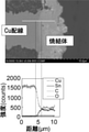
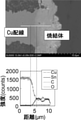
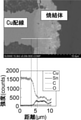
(接合構造の観察及び元素分析)
走査型電子顕微鏡(Scanning Electron Microscope、SEM)で接合構造を観察した。観察したSEM画像を図1に示す。
さらに、エネルギー分散型X線分析(Energy Dispersive X−ray Spectroscopy、EDX)を用いて、加速電圧15kVの条件で接合構造の元素分析を行った。元素分析により得られた各元素(Cu、Sn、C及びO)の強度を図1〜図3に示す。
なお、図1〜図3では、実施例1の接合構造に対して接合領域の幅方向に元素分析を行ったときの測定箇所と、測定により得られたグラフとの関係を示している。
また、図1〜図3の元素分析により得られたグラフについて、点線で挟まれた領域が接合領域に相当する。
(Observation of joint structure and elemental analysis)
The bonding structure was observed with a scanning electron microscope (SEM). The observed SEM image is shown in FIG.
Furthermore, using energy dispersive X-ray analysis (Energy Dispersive X-ray Spectroscopy, EDX), elemental analysis of the junction structure was performed under the condition of an acceleration voltage of 15 kV. The intensities of each element (Cu, Sn, C and O) obtained by elemental analysis are shown in FIGS. 1 to 3.
It should be noted that FIGS. 1 to 3 show the relationship between the measurement points when the elemental analysis is performed in the width direction of the joint region with respect to the joint structure of Example 1 and the graph obtained by the measurement.
Further, in the graphs obtained by the elemental analysis of FIGS. 1 to 3, the region sandwiched by the dotted line corresponds to the junction region.
図1〜図3に示すようにCu配線と焼結体との界面において、Cu配線に含まれないSnの比率が増加し始める箇所からSnの比率が一定になる、あるいは減少する傾向を示し始めた箇所を接合領域として確認した。 As shown in FIGS. 1 to 3, at the interface between the Cu wiring and the sintered body, the Sn ratio starts to become constant or decrease from the point where the Sn ratio not contained in the Cu wiring starts to increase. The location was confirmed as the junction area.
図1〜図3に示すように接合領域では、C及びOの検出強度は小さく、電気伝導を妨げる樹脂の存在が少ない状態であることが確認された。
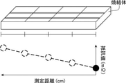
さらに、実施例1の接合構造の焼結体とCu配線との間の接触抵抗を以下のようにして測定した。
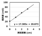
まず、図4に示すようなCu配線が設けられた板状の樹脂基板を用意し、樹脂基板の主面の端部をマスクした状態で当該端部と接続する側面に前述の電磁波シールド用組成物を付与し、前述と同様の条件にて加熱処理して焼結体を形成した。形成された焼結体に抵抗測定用のプローブの片方を接触させ、そこから所定の距離離れた部分のCu配線にもう片方の抵抗測定用のプローブを接触させて抵抗を測定した。
Cu配線の測定位置と抵抗値との関係を図5に示す。図5に示すように、切片が接合領域である部分の接触抵抗の値を意味し、20mΩ程度であった。
以上により、実施例1では、接合領域にて接触抵抗の少ない接合構造が得られていた。
As shown in FIGS. 1 to 3, it was confirmed that the detection intensities of C and O were small in the junction region, and the presence of the resin that hindered electrical conduction was small.
Further, the contact resistance between the sintered body of the bonded structure of Example 1 and the Cu wiring was measured as follows.
First, a plate-shaped resin substrate provided with Cu wiring as shown in FIG. 4 is prepared, and the above-mentioned electromagnetic wave shielding composition is provided on a side surface connected to the end portion of the main surface of the resin substrate in a masked state. The material was added and heat-treated under the same conditions as described above to form a sintered body. One of the probes for resistance measurement was brought into contact with the formed sintered body, and the other probe for resistance measurement was brought into contact with the Cu wiring at a portion separated from the probe for measuring resistance to measure the resistance.
FIG. 5 shows the relationship between the measurement position of the Cu wiring and the resistance value. As shown in FIG. 5, it means the value of the contact resistance of the portion where the section is the junction region, and is about 20 mΩ.
From the above, in Example 1, a bonding structure having a low contact resistance was obtained in the bonding region.
Claims (7)
前記接合領域は、前記金属部材側から前記焼結体側の方向にて、前記金属部材に含まれる金属成分の質量比率が減少し、前記金属部材に含まれず、かつ前記金属粒子Bに含まれる金属成分の質量比率が増加する領域である接合構造。 It contains a metal member, metal particles A, metal particles B having a melting point lower than that of the metal particles A, and a resin, and transitional liquid phase sintering is performed between the metal particles A and the metal particles B. It has a bonding region in which it is bonded to a sintered body of a possible electromagnetic shielding composition.
In the joint region, the mass ratio of the metal component contained in the metal member decreases in the direction from the metal member side to the sintered body side, and the metal not contained in the metal member and contained in the metal particles B. A bonded structure that is a region where the mass ratio of components increases.
Priority Applications (1)
| Application Number | Priority Date | Filing Date | Title |
|---|---|---|---|
| JP2020107307A JP2022001663A (en) | 2020-06-22 | 2020-06-22 | Joined structure and semiconductor package |
Applications Claiming Priority (1)
| Application Number | Priority Date | Filing Date | Title |
|---|---|---|---|
| JP2020107307A JP2022001663A (en) | 2020-06-22 | 2020-06-22 | Joined structure and semiconductor package |
Publications (1)
| Publication Number | Publication Date |
|---|---|
| JP2022001663A true JP2022001663A (en) | 2022-01-06 |
Family
ID=79244080
Family Applications (1)
| Application Number | Title | Priority Date | Filing Date |
|---|---|---|---|
| JP2020107307A Pending JP2022001663A (en) | 2020-06-22 | 2020-06-22 | Joined structure and semiconductor package |
Country Status (1)
| Country | Link |
|---|---|
| JP (1) | JP2022001663A (en) |
Citations (8)
| Publication number | Priority date | Publication date | Assignee | Title |
|---|---|---|---|---|
| JP2012174332A (en) * | 2011-02-17 | 2012-09-10 | Fujitsu Ltd | Conductive jointing material, method of jointing conductor, and method of manufacturing semiconductor |
| JP2013510240A (en) * | 2009-11-05 | 2013-03-21 | オーメット サーキッツ インク | Preparation of metallurgical network compositions and methods of use thereof |
| WO2015105089A1 (en) * | 2014-01-07 | 2015-07-16 | 株式会社村田製作所 | Repair method and repair material |
| JP2017508622A (en) * | 2013-12-31 | 2017-03-30 | アルファ・メタルズ・インコーポレイテッドAlpha Metals, Inc. | Rosin-free thermosetting flux formulation |
| WO2017170398A1 (en) * | 2016-03-29 | 2017-10-05 | タツタ電線株式会社 | Conductive coating material and production method for shielded package using conductive coating material |
| JP2018515348A (en) * | 2015-04-28 | 2018-06-14 | オルメット・サーキッツ・インコーポレイテッド | High metal loading sintered paste for semiconductor die bonding applications |
| JP2018150614A (en) * | 2017-03-10 | 2018-09-27 | 有限会社 ナプラ | Metal particle |
| WO2019117041A1 (en) * | 2017-12-11 | 2019-06-20 | 株式会社弘輝 | Solder paste, joint structure, and method for producing joint structure |
-
2020
- 2020-06-22 JP JP2020107307A patent/JP2022001663A/en active Pending
Patent Citations (8)
| Publication number | Priority date | Publication date | Assignee | Title |
|---|---|---|---|---|
| JP2013510240A (en) * | 2009-11-05 | 2013-03-21 | オーメット サーキッツ インク | Preparation of metallurgical network compositions and methods of use thereof |
| JP2012174332A (en) * | 2011-02-17 | 2012-09-10 | Fujitsu Ltd | Conductive jointing material, method of jointing conductor, and method of manufacturing semiconductor |
| JP2017508622A (en) * | 2013-12-31 | 2017-03-30 | アルファ・メタルズ・インコーポレイテッドAlpha Metals, Inc. | Rosin-free thermosetting flux formulation |
| WO2015105089A1 (en) * | 2014-01-07 | 2015-07-16 | 株式会社村田製作所 | Repair method and repair material |
| JP2018515348A (en) * | 2015-04-28 | 2018-06-14 | オルメット・サーキッツ・インコーポレイテッド | High metal loading sintered paste for semiconductor die bonding applications |
| WO2017170398A1 (en) * | 2016-03-29 | 2017-10-05 | タツタ電線株式会社 | Conductive coating material and production method for shielded package using conductive coating material |
| JP2018150614A (en) * | 2017-03-10 | 2018-09-27 | 有限会社 ナプラ | Metal particle |
| WO2019117041A1 (en) * | 2017-12-11 | 2019-06-20 | 株式会社弘輝 | Solder paste, joint structure, and method for producing joint structure |
Similar Documents
| Publication | Publication Date | Title |
|---|---|---|
| DE19649893B4 (en) | Electrically conductive adhesive and its use | |
| JP7279639B2 (en) | Bonded body manufacturing method and bonding material | |
| KR101886085B1 (en) | Flux compositon comprising carbon component, solder paste comprising the same and method of soldering | |
| JP7559330B2 (en) | Electromagnetic wave shielding composition, electromagnetic wave shielding sheet, electromagnetic wave shielding sintered body, and electronic component device | |
| US7294289B2 (en) | Conductive powder and method for preparing the same | |
| JP6838686B2 (en) | A method for manufacturing electronic component devices and a laminated film used for this method. | |
| JPWO2021019877A1 (en) | How to manufacture electronic component equipment | |
| WO2021038986A1 (en) | Method for manufacturing electronic component device and electronic component device | |
| EP1947656A1 (en) | Ptc device | |
| JP2024023640A (en) | Electromagnetic shielding compositions, electromagnetic shielding sheets, electromagnetic shielding films, and electronic component devices | |
| JP2022001663A (en) | Joined structure and semiconductor package | |
| WO2021060525A1 (en) | Composition for electromagnetic shielding, sheet for electromagnetic shielding, sintered body for electromagnetic shielding, and electronic component device | |
| JP7676763B2 (en) | Electronic component device and method for manufacturing electronic component device | |
| JP7718491B2 (en) | METHOD FOR MANUFACTURING ELECTRONIC COMPONENT DEVICE AND ELECTRONIC COMPONENT DEVICE | |
| TWI451504B (en) | Method of fabricating a semiconductor package or circuit assembly using a reflow underfill composition applied to a solder joint during the impregnation process | |
| JP2022044463A (en) | Resin structure with sintered body for electromagnetic wave shield | |
| JP2022002254A (en) | Manufacturing method of article with sintered body for electromagnetic wave shield | |
| JP2022093169A (en) | Manufacturing method of electronic component device and electronic component device | |
| JP2021063262A (en) | Metal paste for joining, method for manufacturing joined body, and joined body | |
| JP2022027173A (en) | Composition for forming thermoelectric conversion element | |
| JP7238894B2 (en) | Composition, bonding material, sintered body, bonded body, and method for manufacturing bonded body | |
| JP7622634B2 (en) | Copper paste for forming sintered copper pillars and method for producing joint body | |
| JP2022061400A (en) | Resin composition, electromagnetic wave shielding sheet, electromagnetic wave shielding film and electronic component device | |
| WO2020179874A1 (en) | Method for manufacturing electronic component device | |
| JP7565685B2 (en) | Manufacturing method of electromagnetic wave shielding film |
Legal Events
| Date | Code | Title | Description |
|---|---|---|---|
| A621 | Written request for application examination |
Free format text: JAPANESE INTERMEDIATE CODE: A621 Effective date: 20230412 |
|
| A977 | Report on retrieval |
Free format text: JAPANESE INTERMEDIATE CODE: A971007 Effective date: 20240220 |
|
| A131 | Notification of reasons for refusal |
Free format text: JAPANESE INTERMEDIATE CODE: A131 Effective date: 20240326 |
|
| A601 | Written request for extension of time |
Free format text: JAPANESE INTERMEDIATE CODE: A601 Effective date: 20240527 |
|
| A521 | Request for written amendment filed |
Free format text: JAPANESE INTERMEDIATE CODE: A523 Effective date: 20240716 |
|
| A131 | Notification of reasons for refusal |
Free format text: JAPANESE INTERMEDIATE CODE: A131 Effective date: 20241119 |
|
| A601 | Written request for extension of time |
Free format text: JAPANESE INTERMEDIATE CODE: A601 Effective date: 20250120 |
|
| A521 | Request for written amendment filed |
Free format text: JAPANESE INTERMEDIATE CODE: A523 Effective date: 20250313 |
|
| A02 | Decision of refusal |
Free format text: JAPANESE INTERMEDIATE CODE: A02 Effective date: 20250708 |
|
| A521 | Request for written amendment filed |
Free format text: JAPANESE INTERMEDIATE CODE: A523 Effective date: 20251008 |