JP2020021908A - Semiconductor device and method for manufacturing the same - Google Patents
Semiconductor device and method for manufacturing the same Download PDFInfo
- Publication number
- JP2020021908A JP2020021908A JP2018146821A JP2018146821A JP2020021908A JP 2020021908 A JP2020021908 A JP 2020021908A JP 2018146821 A JP2018146821 A JP 2018146821A JP 2018146821 A JP2018146821 A JP 2018146821A JP 2020021908 A JP2020021908 A JP 2020021908A
- Authority
- JP
- Japan
- Prior art keywords
- region
- semiconductor
- semiconductor chip
- chip
- substrate
- Prior art date
- Legal status (The legal status is an assumption and is not a legal conclusion. Google has not performed a legal analysis and makes no representation as to the accuracy of the status listed.)
- Pending
Links
Images


Classifications
-
- H—ELECTRICITY
- H10—SEMICONDUCTOR DEVICES; ELECTRIC SOLID-STATE DEVICES NOT OTHERWISE PROVIDED FOR
- H10W—GENERIC PACKAGES, INTERCONNECTIONS, CONNECTORS OR OTHER CONSTRUCTIONAL DETAILS OF DEVICES COVERED BY CLASS H10
- H10W74/00—Encapsulations, e.g. protective coatings
- H10W74/10—Encapsulations, e.g. protective coatings characterised by their shape or disposition
- H10W74/111—Encapsulations, e.g. protective coatings characterised by their shape or disposition the semiconductor body being completely enclosed
- H10W74/114—Encapsulations, e.g. protective coatings characterised by their shape or disposition the semiconductor body being completely enclosed by a substrate and the encapsulations
-
- H—ELECTRICITY
- H10—SEMICONDUCTOR DEVICES; ELECTRIC SOLID-STATE DEVICES NOT OTHERWISE PROVIDED FOR
- H10W—GENERIC PACKAGES, INTERCONNECTIONS, CONNECTORS OR OTHER CONSTRUCTIONAL DETAILS OF DEVICES COVERED BY CLASS H10
- H10W74/00—Encapsulations, e.g. protective coatings
- H10W74/10—Encapsulations, e.g. protective coatings characterised by their shape or disposition
- H10W74/111—Encapsulations, e.g. protective coatings characterised by their shape or disposition the semiconductor body being completely enclosed
-
- H—ELECTRICITY
- H10—SEMICONDUCTOR DEVICES; ELECTRIC SOLID-STATE DEVICES NOT OTHERWISE PROVIDED FOR
- H10D—INORGANIC ELECTRIC SEMICONDUCTOR DEVICES
- H10D62/00—Semiconductor bodies, or regions thereof, of devices having potential barriers
- H10D62/10—Shapes, relative sizes or dispositions of the regions of the semiconductor bodies; Shapes of the semiconductor bodies
-
- H—ELECTRICITY
- H10—SEMICONDUCTOR DEVICES; ELECTRIC SOLID-STATE DEVICES NOT OTHERWISE PROVIDED FOR
- H10P—GENERIC PROCESSES OR APPARATUS FOR THE MANUFACTURE OR TREATMENT OF DEVICES COVERED BY CLASS H10
- H10P54/00—Cutting or separating of wafers, substrates or parts of devices
-
- H—ELECTRICITY
- H10—SEMICONDUCTOR DEVICES; ELECTRIC SOLID-STATE DEVICES NOT OTHERWISE PROVIDED FOR
- H10P—GENERIC PROCESSES OR APPARATUS FOR THE MANUFACTURE OR TREATMENT OF DEVICES COVERED BY CLASS H10
- H10P72/00—Handling or holding of wafers, substrates or devices during manufacture or treatment thereof
- H10P72/70—Handling or holding of wafers, substrates or devices during manufacture or treatment thereof for supporting or gripping
- H10P72/74—Handling or holding of wafers, substrates or devices during manufacture or treatment thereof for supporting or gripping using temporarily an auxiliary support
- H10P72/7402—Wafer tapes, e.g. grinding or dicing support tapes
-
- H—ELECTRICITY
- H10—SEMICONDUCTOR DEVICES; ELECTRIC SOLID-STATE DEVICES NOT OTHERWISE PROVIDED FOR
- H10W—GENERIC PACKAGES, INTERCONNECTIONS, CONNECTORS OR OTHER CONSTRUCTIONAL DETAILS OF DEVICES COVERED BY CLASS H10
- H10W72/00—Interconnections or connectors in packages
- H10W72/30—Die-attach connectors
-
- H—ELECTRICITY
- H10—SEMICONDUCTOR DEVICES; ELECTRIC SOLID-STATE DEVICES NOT OTHERWISE PROVIDED FOR
- H10W—GENERIC PACKAGES, INTERCONNECTIONS, CONNECTORS OR OTHER CONSTRUCTIONAL DETAILS OF DEVICES COVERED BY CLASS H10
- H10W72/00—Interconnections or connectors in packages
- H10W72/50—Bond wires
-
- H—ELECTRICITY
- H10—SEMICONDUCTOR DEVICES; ELECTRIC SOLID-STATE DEVICES NOT OTHERWISE PROVIDED FOR
- H10W—GENERIC PACKAGES, INTERCONNECTIONS, CONNECTORS OR OTHER CONSTRUCTIONAL DETAILS OF DEVICES COVERED BY CLASS H10
- H10W72/00—Interconnections or connectors in packages
- H10W72/90—Bond pads, in general
-
- H—ELECTRICITY
- H10—SEMICONDUCTOR DEVICES; ELECTRIC SOLID-STATE DEVICES NOT OTHERWISE PROVIDED FOR
- H10W—GENERIC PACKAGES, INTERCONNECTIONS, CONNECTORS OR OTHER CONSTRUCTIONAL DETAILS OF DEVICES COVERED BY CLASS H10
- H10W90/00—Package configurations
-
- H—ELECTRICITY
- H10—SEMICONDUCTOR DEVICES; ELECTRIC SOLID-STATE DEVICES NOT OTHERWISE PROVIDED FOR
- H10W—GENERIC PACKAGES, INTERCONNECTIONS, CONNECTORS OR OTHER CONSTRUCTIONAL DETAILS OF DEVICES COVERED BY CLASS H10
- H10W90/00—Package configurations
- H10W90/20—Configurations of stacked chips
- H10W90/28—Configurations of stacked chips the stacked chips having different sizes, e.g. chip stacks having a pyramidal shape
-
- H—ELECTRICITY
- H10—SEMICONDUCTOR DEVICES; ELECTRIC SOLID-STATE DEVICES NOT OTHERWISE PROVIDED FOR
- H10P—GENERIC PROCESSES OR APPARATUS FOR THE MANUFACTURE OR TREATMENT OF DEVICES COVERED BY CLASS H10
- H10P72/00—Handling or holding of wafers, substrates or devices during manufacture or treatment thereof
- H10P72/70—Handling or holding of wafers, substrates or devices during manufacture or treatment thereof for supporting or gripping
- H10P72/74—Handling or holding of wafers, substrates or devices during manufacture or treatment thereof for supporting or gripping using temporarily an auxiliary support
- H10P72/7416—Handling or holding of wafers, substrates or devices during manufacture or treatment thereof for supporting or gripping using temporarily an auxiliary support used during dicing or grinding
-
- H—ELECTRICITY
- H10—SEMICONDUCTOR DEVICES; ELECTRIC SOLID-STATE DEVICES NOT OTHERWISE PROVIDED FOR
- H10W—GENERIC PACKAGES, INTERCONNECTIONS, CONNECTORS OR OTHER CONSTRUCTIONAL DETAILS OF DEVICES COVERED BY CLASS H10
- H10W72/00—Interconnections or connectors in packages
- H10W72/071—Connecting or disconnecting
- H10W72/073—Connecting or disconnecting of die-attach connectors
- H10W72/07351—Connecting or disconnecting of die-attach connectors characterised by changes in properties of the die-attach connectors during connecting
- H10W72/07354—Connecting or disconnecting of die-attach connectors characterised by changes in properties of the die-attach connectors during connecting changes in dispositions
-
- H—ELECTRICITY
- H10—SEMICONDUCTOR DEVICES; ELECTRIC SOLID-STATE DEVICES NOT OTHERWISE PROVIDED FOR
- H10W—GENERIC PACKAGES, INTERCONNECTIONS, CONNECTORS OR OTHER CONSTRUCTIONAL DETAILS OF DEVICES COVERED BY CLASS H10
- H10W72/00—Interconnections or connectors in packages
- H10W72/30—Die-attach connectors
- H10W72/341—Dispositions of die-attach connectors, e.g. layouts
- H10W72/347—Dispositions of multiple die-attach connectors
-
- H—ELECTRICITY
- H10—SEMICONDUCTOR DEVICES; ELECTRIC SOLID-STATE DEVICES NOT OTHERWISE PROVIDED FOR
- H10W—GENERIC PACKAGES, INTERCONNECTIONS, CONNECTORS OR OTHER CONSTRUCTIONAL DETAILS OF DEVICES COVERED BY CLASS H10
- H10W72/00—Interconnections or connectors in packages
- H10W72/50—Bond wires
- H10W72/541—Dispositions of bond wires
- H10W72/5445—Dispositions of bond wires being orthogonal to a side surface of the chip, e.g. parallel arrangements
-
- H—ELECTRICITY
- H10—SEMICONDUCTOR DEVICES; ELECTRIC SOLID-STATE DEVICES NOT OTHERWISE PROVIDED FOR
- H10W—GENERIC PACKAGES, INTERCONNECTIONS, CONNECTORS OR OTHER CONSTRUCTIONAL DETAILS OF DEVICES COVERED BY CLASS H10
- H10W72/00—Interconnections or connectors in packages
- H10W72/50—Bond wires
- H10W72/59—Bond pads specially adapted therefor
-
- H—ELECTRICITY
- H10—SEMICONDUCTOR DEVICES; ELECTRIC SOLID-STATE DEVICES NOT OTHERWISE PROVIDED FOR
- H10W—GENERIC PACKAGES, INTERCONNECTIONS, CONNECTORS OR OTHER CONSTRUCTIONAL DETAILS OF DEVICES COVERED BY CLASS H10
- H10W72/00—Interconnections or connectors in packages
- H10W72/851—Dispositions of multiple connectors or interconnections
- H10W72/874—On different surfaces
- H10W72/877—Bump connectors and die-attach connectors
-
- H—ELECTRICITY
- H10—SEMICONDUCTOR DEVICES; ELECTRIC SOLID-STATE DEVICES NOT OTHERWISE PROVIDED FOR
- H10W—GENERIC PACKAGES, INTERCONNECTIONS, CONNECTORS OR OTHER CONSTRUCTIONAL DETAILS OF DEVICES COVERED BY CLASS H10
- H10W72/00—Interconnections or connectors in packages
- H10W72/851—Dispositions of multiple connectors or interconnections
- H10W72/874—On different surfaces
- H10W72/884—Die-attach connectors and bond wires
-
- H—ELECTRICITY
- H10—SEMICONDUCTOR DEVICES; ELECTRIC SOLID-STATE DEVICES NOT OTHERWISE PROVIDED FOR
- H10W—GENERIC PACKAGES, INTERCONNECTIONS, CONNECTORS OR OTHER CONSTRUCTIONAL DETAILS OF DEVICES COVERED BY CLASS H10
- H10W72/00—Interconnections or connectors in packages
- H10W72/90—Bond pads, in general
- H10W72/941—Dispositions of bond pads
- H10W72/944—Dispositions of multiple bond pads
- H10W72/9445—Top-view layouts, e.g. mirror arrays
-
- H—ELECTRICITY
- H10—SEMICONDUCTOR DEVICES; ELECTRIC SOLID-STATE DEVICES NOT OTHERWISE PROVIDED FOR
- H10W—GENERIC PACKAGES, INTERCONNECTIONS, CONNECTORS OR OTHER CONSTRUCTIONAL DETAILS OF DEVICES COVERED BY CLASS H10
- H10W74/00—Encapsulations, e.g. protective coatings
-
- H—ELECTRICITY
- H10—SEMICONDUCTOR DEVICES; ELECTRIC SOLID-STATE DEVICES NOT OTHERWISE PROVIDED FOR
- H10W—GENERIC PACKAGES, INTERCONNECTIONS, CONNECTORS OR OTHER CONSTRUCTIONAL DETAILS OF DEVICES COVERED BY CLASS H10
- H10W74/00—Encapsulations, e.g. protective coatings
- H10W74/10—Encapsulations, e.g. protective coatings characterised by their shape or disposition
- H10W74/15—Encapsulations, e.g. protective coatings characterised by their shape or disposition on active surfaces of flip-chip devices, e.g. underfills
-
- H—ELECTRICITY
- H10—SEMICONDUCTOR DEVICES; ELECTRIC SOLID-STATE DEVICES NOT OTHERWISE PROVIDED FOR
- H10W—GENERIC PACKAGES, INTERCONNECTIONS, CONNECTORS OR OTHER CONSTRUCTIONAL DETAILS OF DEVICES COVERED BY CLASS H10
- H10W90/00—Package configurations
- H10W90/20—Configurations of stacked chips
- H10W90/24—Configurations of stacked chips at least one of the stacked chips being laterally offset from a neighbouring stacked chip, e.g. chip stacks having a staircase shape
-
- H—ELECTRICITY
- H10—SEMICONDUCTOR DEVICES; ELECTRIC SOLID-STATE DEVICES NOT OTHERWISE PROVIDED FOR
- H10W—GENERIC PACKAGES, INTERCONNECTIONS, CONNECTORS OR OTHER CONSTRUCTIONAL DETAILS OF DEVICES COVERED BY CLASS H10
- H10W90/00—Package configurations
- H10W90/701—Package configurations characterised by the relative positions of pads or connectors relative to package parts
- H10W90/721—Package configurations characterised by the relative positions of pads or connectors relative to package parts of bump connectors
- H10W90/724—Package configurations characterised by the relative positions of pads or connectors relative to package parts of bump connectors between a chip and a stacked insulating package substrate, interposer or RDL
-
- H—ELECTRICITY
- H10—SEMICONDUCTOR DEVICES; ELECTRIC SOLID-STATE DEVICES NOT OTHERWISE PROVIDED FOR
- H10W—GENERIC PACKAGES, INTERCONNECTIONS, CONNECTORS OR OTHER CONSTRUCTIONAL DETAILS OF DEVICES COVERED BY CLASS H10
- H10W90/00—Package configurations
- H10W90/701—Package configurations characterised by the relative positions of pads or connectors relative to package parts
- H10W90/731—Package configurations characterised by the relative positions of pads or connectors relative to package parts of die-attach connectors
- H10W90/732—Package configurations characterised by the relative positions of pads or connectors relative to package parts of die-attach connectors between stacked chips
-
- H—ELECTRICITY
- H10—SEMICONDUCTOR DEVICES; ELECTRIC SOLID-STATE DEVICES NOT OTHERWISE PROVIDED FOR
- H10W—GENERIC PACKAGES, INTERCONNECTIONS, CONNECTORS OR OTHER CONSTRUCTIONAL DETAILS OF DEVICES COVERED BY CLASS H10
- H10W90/00—Package configurations
- H10W90/701—Package configurations characterised by the relative positions of pads or connectors relative to package parts
- H10W90/731—Package configurations characterised by the relative positions of pads or connectors relative to package parts of die-attach connectors
- H10W90/734—Package configurations characterised by the relative positions of pads or connectors relative to package parts of die-attach connectors between a chip and a stacked insulating package substrate, interposer or RDL
-
- H—ELECTRICITY
- H10—SEMICONDUCTOR DEVICES; ELECTRIC SOLID-STATE DEVICES NOT OTHERWISE PROVIDED FOR
- H10W—GENERIC PACKAGES, INTERCONNECTIONS, CONNECTORS OR OTHER CONSTRUCTIONAL DETAILS OF DEVICES COVERED BY CLASS H10
- H10W90/00—Package configurations
- H10W90/701—Package configurations characterised by the relative positions of pads or connectors relative to package parts
- H10W90/751—Package configurations characterised by the relative positions of pads or connectors relative to package parts of bond wires
- H10W90/752—Package configurations characterised by the relative positions of pads or connectors relative to package parts of bond wires between stacked chips
-
- H—ELECTRICITY
- H10—SEMICONDUCTOR DEVICES; ELECTRIC SOLID-STATE DEVICES NOT OTHERWISE PROVIDED FOR
- H10W—GENERIC PACKAGES, INTERCONNECTIONS, CONNECTORS OR OTHER CONSTRUCTIONAL DETAILS OF DEVICES COVERED BY CLASS H10
- H10W90/00—Package configurations
- H10W90/701—Package configurations characterised by the relative positions of pads or connectors relative to package parts
- H10W90/751—Package configurations characterised by the relative positions of pads or connectors relative to package parts of bond wires
- H10W90/754—Package configurations characterised by the relative positions of pads or connectors relative to package parts of bond wires between a chip and a stacked insulating package substrate, interposer or RDL
Landscapes
- Structures Or Materials For Encapsulating Or Coating Semiconductor Devices Or Solid State Devices (AREA)
- Engineering & Computer Science (AREA)
- Manufacturing & Machinery (AREA)
- Microelectronics & Electronic Packaging (AREA)
- Die Bonding (AREA)
Abstract
【課題】スペーサチップを用いること無く、一方の半導体チップを他方の半導体チップ上方に配置してパッケージサイズを小さくすることができる半導体装置およびその製造方法を提供する。【解決手段】本実施形態による半導体装置は、基板と、第1半導体チップと、第2半導体チップと、接着層と、樹脂層とを備えている。第1半導体チップは、基板の表面上に設けられている。第2半導体チップは、裏面の第1領域において突出している突出部を有する。突出部を基板の表面に接着させたときに、第1領域以外の裏面の第2領域が第1半導体チップまたは該第1半導体チップと基板との間を接続するワイヤの少なくとも一部分の上方に第1半導体チップに接することなく配置される。接着層は、第1領域と基板との間および第2領域と基板との間に設けられている。樹脂層は、基板上に設けられ、第1および第2半導体チップを被覆する。【選択図】図1PROBLEM TO BE SOLVED: To provide a semiconductor device capable of arranging one semiconductor chip above the other semiconductor chip to reduce the package size without using a spacer chip, and a method for manufacturing the same. A semiconductor device according to the present embodiment includes a substrate, a first semiconductor chip, a second semiconductor chip, an adhesive layer, and a resin layer. The first semiconductor chip is provided on the surface of the substrate. The second semiconductor chip has a protruding portion that protrudes in the first region on the back surface. When the protrusion is adhered to the front surface of the substrate, the second region on the back surface other than the first region is located above the first semiconductor chip or at least a part of the wire connecting the first semiconductor chip and the substrate. 1 Arranged without contacting a semiconductor chip. The adhesive layer is provided between the first region and the substrate and between the second region and the substrate. The resin layer is provided on the substrate and covers the first and second semiconductor chips. [Selection diagram] Fig. 1
Description
本実施形態は、半導体装置およびその製造方法に関する。 This embodiment relates to a semiconductor device and a method for manufacturing the same.
メモリチップおよびそのコントローラチップのように、複数の半導体チップを1つのパッケージ内に封止する場合がある。この場合、例えば、メモリチップをスペーサチップで嵩上げして、コントローラチップ上方に重複させて配置するパッケージ構造がある。このようなパッケージ構造は、複数の半導体チップを単純に横並びに配置した構造よりもパッケージ全体のサイズを小さくすることができる。 A plurality of semiconductor chips, such as a memory chip and its controller chip, may be sealed in one package. In this case, for example, there is a package structure in which a memory chip is raised with a spacer chip and is arranged so as to overlap above the controller chip. Such a package structure can reduce the size of the entire package as compared with a structure in which a plurality of semiconductor chips are simply arranged side by side.
しかし、メモリチップを嵩上げするために、スペーサチップが必要となるので、コスト高となる。 However, since a spacer chip is required to raise the memory chip, the cost increases.
また、スペーサチップの代わりに厚いDAF(Die Attachment Film)を用いた場合、メモリチップは傾斜し易くなる。あるいは、メモリチップ自体の形状が歪んでしまうおそれもある。メモリチップが傾斜しあるいは歪むと、メモリチップ上にさらに他のメモリチップを積層する場合に、積層したメモリチップが剥がれやすくなり、ボンディングワイヤを接続し難くなる。また、DAFがつぶれると、メモリチップがその下のコントローラチップと接触するおそれがある。さらに、DAFがつぶれると、DAFがメモリチップの下からボンディングパッドへとはみ出し、その後、金属ワイヤをボンディングパッドへボンディングすることが困難になることもある。 When a thick DAF (Die Attachment Film) is used in place of the spacer chip, the memory chip tends to tilt. Alternatively, the shape of the memory chip itself may be distorted. When the memory chip is tilted or distorted, when another memory chip is stacked on the memory chip, the stacked memory chip is easily peeled off, and it is difficult to connect a bonding wire. Also, if the DAF is crushed, the memory chip may come into contact with the controller chip therebelow. Further, when the DAF is crushed, the DAF may protrude from under the memory chip to the bonding pad, and thereafter, it may be difficult to bond the metal wire to the bonding pad.
スペーサチップを用いること無く、一方の半導体チップを他方の半導体チップ上方に配置してパッケージサイズを小さくすることができる半導体装置およびその製造方法を提供する。 Provided is a semiconductor device capable of reducing a package size by disposing one semiconductor chip above another semiconductor chip without using a spacer chip, and a method for manufacturing the same.
本実施形態による半導体装置は、基板と、第1半導体チップと、第2半導体チップと、接着層と、樹脂層とを備えている。第1半導体チップは、基板の表面上に設けられている。第2半導体チップは、裏面の第1領域において突出している突出部を有する。突出部を基板の表面に接着させたときに、第1領域以外の裏面の第2領域が第1半導体チップまたは該第1半導体チップと基板との間を接続するワイヤの少なくとも一部分の上方に第1半導体チップに接することなく配置される。接着層は、第1領域と基板との間および第2領域と基板との間に設けられている。樹脂層は、基板上に設けられ、第1および第2半導体チップを被覆する。 The semiconductor device according to the present embodiment includes a substrate, a first semiconductor chip, a second semiconductor chip, an adhesive layer, and a resin layer. The first semiconductor chip is provided on a surface of the substrate. The second semiconductor chip has a protruding portion that protrudes in the first region on the back surface. When the protruding portion is bonded to the front surface of the substrate, the second region on the back surface other than the first region is positioned above at least a portion of the first semiconductor chip or at least a portion of a wire connecting the first semiconductor chip and the substrate. It is arranged without touching one semiconductor chip. The adhesive layer is provided between the first region and the substrate and between the second region and the substrate. The resin layer is provided on the substrate and covers the first and second semiconductor chips.
以下、図面を参照して本発明に係る実施形態を説明する。本実施形態は、本発明を限定するものではない。以下の実施形態において、上下方向は、半導体チップを基板に実装する面を上とした場合の相対方向を示し、重力加速度に従った上下方向と異なる場合がある。図面は模式的または概念的なものであり、各部分の比率などは、必ずしも現実のものと同一とは限らない。明細書と図面において、既出の図面に関して前述したものと同様の要素には同一の符号を付して詳細な説明は適宜省略する。 Hereinafter, embodiments of the present invention will be described with reference to the drawings. This embodiment does not limit the present invention. In the following embodiments, the up-down direction indicates a relative direction when the surface on which the semiconductor chip is mounted on the substrate is upward, and may be different from the up-down direction according to the gravitational acceleration. The drawings are schematic or conceptual, and the proportions and the like of each part are not always the same as actual ones. In the specification and drawings, the same reference numerals are given to the same elements as those described above with respect to the already-explained drawings, and the detailed description will be appropriately omitted.
(第1実施形態)
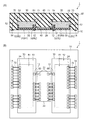
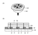
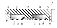
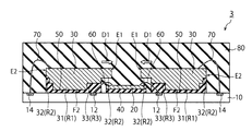
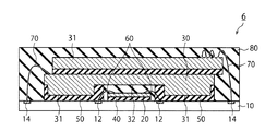
図1(A)および図1(B)は、第1実施形態による半導体装置1の構成例を示す断面図および平面図である。半導体装置1は、樹脂基板10と、コントローラチップ20と、メモリチップ30と、接着層40、50と、金属ワイヤ60、70と、モールド樹脂80とを備えている。本実施形態の半導体装置1は、面実装型の半導体パッケージであり、例えば、BGA(Ball Grid Array package)、LGA(Land Grid Array Package)等でよい。半導体装置1は、例えば、NAND型フラッシュメモリ等の半導体記憶装置でもよい。
(1st Embodiment)
1A and 1B are a cross-sectional view and a plan view illustrating a configuration example of the
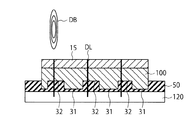
基板としての樹脂基板10は、例えば、複数の絶縁層と複数の配線層(いずれも図示せず)とを積層して一体化した多層配線基板でよい。絶縁層には、例えば、ガラスエポキシ樹脂、有機高分子材料またはセラミックス材料(例えば、酸化アルミニウム(Al2O3))等の樹脂材料を用いる。配線層は、樹脂基板10内に設けられ、ボンディングパッドに電気的に接続されている。配線層には、例えば、銅などの低抵抗の導電性材料を用いている。樹脂基板10の平面形状は、特に限定しないが、図1(B)に示すように、略長方形あるいは略正方形でよい。
The
樹脂基板10の表面上には、ボンディングパッド12、14が設けられている。ボンディングパッド12、14には、金属ワイヤ60、70がボンディングされている。金属ワイヤ60、70には、例えば、金が用いられている。
第1半導体チップとしてのコントローラチップ20は、樹脂基板10の表面上に接着層(DAF(Die Attachment Film))40で接着され固定されている。コントローラチップ20は、メモリチップ30を制御する半導体チップであり、半導体基板の表面に制御回路を構成する半導体素子(例えば、トランジスタ等)が設けられている。また、コントローラチップ20は、内部の制御回路に接続されたボンディングパッド22を有し、ボンディングパッド22は、金属ワイヤ60によって樹脂基板10のボンディングパッド12と電気的に接続されている。
The
第2半導体チップとしてのメモリチップ30は、樹脂基板10の表面上に接着層(DAF)50で接着され固定されている。メモリチップ30は、例えば、NAND型フラッシュメモリを有する半導体チップであり、半導体基板の表面上に平面型または立体型のメモリセルアレイが設けられている。また、メモリチップ30は、内部回路に接続されたボンディングパッド24を有し、ボンディングパッド24は、金属ワイヤ70によって樹脂基板10のボンディングパッド14と電気的に接続されている。これにより、メモリチップ30は、金属ワイヤ60、70および樹脂基板10の内部配線を介してコントローラチップ20と電気的に接続され、コントローラチップ20の制御を受けて動作することができる。
The
図1(A)に示すように、メモリチップ30の裏面は、第1領域R1において突出している突出部31を有する。また、メモリチップ30の裏面は、第1領域R1以外の裏面の第2領域R2において窪んでいる凹部を有する。突出部31を樹脂基板10の表面に接着させたときに、第2領域R2の凹部32は、コントローラチップ20と樹脂基板10との間を接続する金属ワイヤ60の少なくとも一部分の上方に重複するように位置する。このとき、凹部32は、コントローラチップ20および金属ワイヤ60には接触していない。
As shown in FIG. 1A, the back surface of the
接着層50は、第1領域R1と樹脂基板10との間に設けられており、突出部31を樹脂基板10上に接着する。それとともに、接着層50は、第2領域R2と樹脂基板10との間にも設けられており、凹部32を樹脂基板10に接着している。また、第2領域R2と樹脂基板10との間にある接着層50は、金属ワイヤ60の一部およびボンディングパッド12に接触しており、これらを被覆している。即ち、樹脂基板10の表面上方から見たときに、メモリチップ30の第2領域R2は、金属ワイヤ60の少なくとも一部と重複している。
The
このように、メモリチップ30の裏面に突出部31および凹部32を設けることによって、メモリチップ30をコントローラチップ20および金属ワイヤ60に接触させることなく、メモリチップ30の第2領域R2をコントローラチップ20側へせり出すことができる。これにより、メモリチップ30をコントローラチップ20または金属ワイヤ60の上方に重複させることができ、半導体装置1の全体のサイズを小さくすることができる。
As described above, by providing the protruding
第2領域R2をコントローラチップ20側へせり出しても、メモリチップ30がコントローラチップ20に接触しないように、第2領域R2と第1領域R1とにおけるメモリチップ30の厚みの差は、コントローラチップ20の厚みよりも大きいことが好ましい。また、第2領域R2をコントローラチップ20側へせり出しても、金属ワイヤ60がコントローラチップ20に接触しないように、第2領域R2と第1領域R1とにおけるメモリチップ30の厚みの差は、金属ワイヤ60の高さよりも大きいことが好ましい。
The difference between the thickness of the
モールド樹脂80は、樹脂基板10上に設けられ、コントローラチップ20、メモリチップ30、金属ワイヤ60、70を被覆する。モールド樹脂80は、コントローラチップ20、メモリチップ30、金属ワイヤ60、70を半導体装置1の外部から保護している。
The
図1(B)に示すように、第1領域R1は、第2領域R2の内側にあり第2領域R2の外側にははみ出していない。また、図1(A)に示すようにコントローラチップ20およびメモリチップ30の配列方向に切断した断面において、第2領域R2は、メモリチップ30からコントローラチップ20へ向かう第1方向D1と第1方向D1とは逆の第2方向D2との両方へ延伸している。この場合、接着層50が第1領域R1からはみ出したときに、第2領域R2は、はみ出した接着層50を受容して、接着層50が横方向へ広がることを抑制することができる。即ち、第2領域R2がメモリチップ30の両側からD1およびD2方向へ延伸している場合、接着層50は、端部E1における第2領域R2と樹脂基板10との間、並びに、端部E2における第2領域R2と樹脂基板10との間に受容される。
As shown in FIG. 1B, the first region R1 is inside the second region R2 and does not protrude outside the second region R2. Further, as shown in FIG. 1A, in a cross section cut in the arrangement direction of the
コントローラチップ20に近い端部E1において第2領域R2が設けられていれている必要はあるが、コントローラチップ20から離れた端部E2において第2領域R2は必ずしも設けられていなくてもよい。即ち、第2領域R2は、第2方向D2へ延伸している必要は必ずしも無い。この場合でも、メモリチップ30を金属ワイヤ60の上方に重複させることができる。また、第1領域R1の端部E1からD1方向へはみ出した接着層50は、第2領域R2に受容され、金属ワイヤ60の一部を被覆することができる。
Although the second region R2 needs to be provided at the end E1 near the
尚、金属ワイヤ60はメモリチップ30の接着前に接合されているので、接着層50はボンディングパッド12および金属ワイヤ60に接触しても構わない。寧ろ、接着層50がボンディングパッド12および金属ワイヤ60を被覆することによって、接着層50は、ボンディングパッド12および金属ワイヤ60を保護することができる。
Since the
一方、端部E2に第2領域R2が設けられていない場合、第1領域R1の端部E2からD2方向へはみ出した接着層50は、受容されずに、横方向へ広がる場合がある。金属ワイヤ70はメモリチップ30の接着後に接合されるので、メモリチップ30の搭載時に接着層50がボンディングパッド14まではみ出すと、金属ワイヤ70をボンディングパッド14に接合させることができないおそれがある。従って、第2領域R2は、端部E2にも設けられていることが好ましい。しかし、接着層50が横方向へ広がったとしても、ボンディングパッド14や金属ワイヤ70に影響を与えなければ、第2領域R2は、端部E2に設けられていなくてもよい。
On the other hand, when the second region R2 is not provided at the end E2, the
また、図1(B)に示すように、樹脂基板10の上方から見た平面視において、第2領域R2は、第1領域R1を取り囲むように、第1領域R1の外周全体に設けられていてもよい。この場合、D1、D2方向へはみ出した接着層50だけでなく、裏面F2面内においてD1、D2方向に対して略直行方向へはみ出した接着層50も第2領域R2と樹脂基板10との間で受容することができる。その結果、接着層50が過剰に広がることを抑制することができる。
In addition, as shown in FIG. 1B, in plan view when viewed from above the
本実施形態では、複数のメモリチップ30がコントローラチップ20の両側に分離して設けられている。この場合、コントローラチップ20の直上には、メモリチップ30は設けられていないので、複数のメモリチップ30間には、モールド樹脂80が設けられている。これにより、メモリチップ30、コントローラチップ20および金属ワイヤ60、70は、モールド樹脂80で保護される。金属ワイヤ60の一部とボンディングパッド12は、接着層50で保護される。
In the present embodiment, a plurality of
本実施形態によれば、メモリチップ30の裏面の第1領域R1には突出部31を有する。突出部31を樹脂基板10の表面に接着させたとき、メモリチップ30の第2領域R2が金属ワイヤ60の少なくとも一部分の上方に、コントローラチップ20に接触することなく配置される。樹脂基板10の表面上方から見た平面視では、第2領域R2は、金属ワイヤ60の少なくとも一部と重複している。これにより、コントローラチップ20およびメモリチップ30を単に横並びに並列させたパッケージ構造よりも、本実施形態に従ったパッケージ構造のサイズは小さくなる。
According to the present embodiment, the first region R <b> 1 on the back surface of the
さらに、メモリチップ30の端部E1側の第2領域R2の下には、接着層50が設けられている。これにより、接着層50が金属ワイヤ60の一部およびボンディングパッド12を被覆してこれらを保護することができる。
Further, an
また、端部E2側の第2領域R2の下には、接着層50が受容され得る。これにより、メモリチップ30の搭載時に、接着層50がメモリチップ30からボンディングパッド14まではみ出さず、ボンディングパッド14の汚染等を抑制することができる。
The
さらに、第2領域R2が第1領域R1の外周全体に設けられていることによって、接着層50がメモリチップ30からはみ出すことをさらに効果的に抑制することができる。
Further, since the second region R2 is provided on the entire outer periphery of the first region R1, the protrusion of the
次に、本実施形態による半導体装置1の製造方法について説明する。
Next, the method for manufacturing the
図2(A)〜図6(B)は、第1実施形態による半導体装置1の製造方法の一例を示す図である。尚、以下の半導体チップの製造方法は、コントローラチップ20およびメモリチップ30のいずれにも適用可能である。
FIGS. 2A to 6B are views illustrating an example of a method of manufacturing the
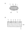
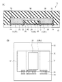
まず、図2(A)および図2(B)に示すように、半導体ウェハ100の表面F1上に、半導体素子15を形成する。各半導体チップ間には、ダイシングラインDLが設けられている。尚、図2(B)は、図2(A)の一部の断面図である。
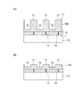
次に、図3(A)に示すように、半導体ウェハ100の表面F1に保護テープ110が貼付され、図3(B)に示すように、半導体ウェハ100の裏面F2をCMP(Chemical Mechanical Polishing)法により研磨する。
First, as shown in FIGS. 2A and 2B, the
Next, as shown in FIG. 3A, a
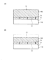
次に、図4(A)に示すように、半導体ウェハ100の裏面F2の第2領域R2をトリムブレードTBで切削する。これにより、裏面F2の第1領域R1において突出している突出部31と、それ以外の裏面F2の第2領域R2において窪んでいる凹部32とを形成する。
Next, as shown in FIG. 4A, the second region R2 on the back surface F2 of the
次に、図4(B)に示すように、接着層50を有するダイシングテープ120上に、裏面F2を接着層50へ向けて半導体ウェハ100を搭載する。さらに、図5(A)に示すように、半導体ウェハ100をダイシングテープ120へ加圧することによって、半導体ウェハ100の凹部32内に接着層50を埋め込む。
Next, as shown in FIG. 4B, the
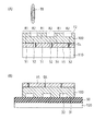
次に、図5(B)に示すように、レーザ発振器130を用いて、半導体ウェハ100の裏面F2のダイシングラインDLに対応する部分にレーザ光を照射する。これにより、半導体ウェハ100の内部に改質層LMを形成する。
Next, as shown in FIG. 5B, a portion corresponding to the dicing line DL on the back surface F2 of the
次に、図6(A)に示すように、ダイシングテープ120を下方から押上部材140で押し上げることによって、ダイシングテープ120を引っ張る(エキスパンドさせる)。これにより、ダイシングテープ120とともに半導体ウェハ100が外方向へ引っ張られる。このとき、図6(B)に示すように、半導体ウェハ100および接着層50が改質層LMに沿って(即ち、ダイシングラインに沿って)劈開され、複数の半導体チップに個片化される。
Next, as shown in FIG. 6A, the dicing
その後、半導体チップ(コントローラチップ20および/またはメモリチップ30)は、それぞれピックアップされて樹脂基板10上に実装される。
Thereafter, the semiconductor chips (
例えば、コントローラチップ20を樹脂基板10上に実装する。このとき、図1に示すように、接着層40がコントローラチップ20を樹脂基板10上に接着する。このとき、接着層40を加熱して、コントローラチップ20を樹脂基板10上に接着してもよい。
For example, the
次に、金属ワイヤ60でコントローラチップ20と樹脂基板10のボンディングパッド12とを接合する。
Next, the
次に、メモリチップ30を樹脂基板10上に実装する。このとき、図1に示すように、接着層50がメモリチップ30を樹脂基板10上に接着する。接着層50を加熱して、メモリチップ30を樹脂基板10上に接着してもよい。このとき、メモリチップ30の突出部31を樹脂基板10の表面に接着層50で接着するとともに、凹部32を金属ワイヤ60の上方に配置する。
Next, the
メモリチップ30は、その端部E1が金属ワイヤ60の上方にせり出すように配置され、金属ワイヤ60の一部と重複している。これにより、半導体装置1のサイズを小さくすることができる。それとともに、メモリチップ30の端部E1側の接着層50は、金属ワイヤ60の一部やボンディングパッド12を埋め込み、これらを保護することができる。
The
本実施形態では、2つのメモリチップ30がコントローラチップ20の両側に配置され、コントローラチップ20の両側で接着層50が金属ワイヤ60やボンディングパッド12を保護している。
In this embodiment, two
次に、コントローラチップ20およびメモリチップ30がモールド樹脂80によって封止される。これにより、図1に示す半導体装置1のパッケージが完成する。
Next, the
本実施形態によれば、メモリチップ30の突出部31を樹脂基板10の表面に接着させたとき、メモリチップ30の凹部32を金属ワイヤ60に接触させることなくその上方に配置することができる。これにより、スペーサチップ等を用いること無く、メモリチップ30の一部をコントローラチップ20の上方に重複させ、パッケージ構造のサイズを小さくすることができる。
According to the present embodiment, when the protruding
さらに、メモリチップ30の端部E1側の第2領域R2の下には、接着層50が設けられている。これにより、接着層50が金属ワイヤ60の一部およびボンディングパッド12を被覆してこれらを保護することができる。
Further, an
また、端部E2側の第2領域R2の下には、接着層50が受容され得る。これにより、メモリチップ30の搭載時に、接着層50がボンディングパッド14まではみ出さず、ボンディングパッド14の汚染等を抑制することができる。
The
(変形例1)
図7は、第1実施形態の変形例1による半導体装置1の製造方法を示す図である。第1実施形態による製造方法では、図5(A)に示すように、接着層50で凹部32を充填した後、レーザダイシングおよびエキスパンドによって半導体チップを個片化している。
(Modification 1)
FIG. 7 is a diagram illustrating the method of manufacturing the
しかし、変形例1では、レーザダイシングおよびエキスパンドに代えて、ブレードダイシングを行う。ブレードダイシングでは、図7のダイシングブレードDBを用いて、ダイシングラインDLをカットする。 However, in the first modification, blade dicing is performed instead of laser dicing and expanding. In blade dicing, the dicing line DL is cut using the dicing blade DB in FIG.
トリムブレードの幅(回転面に対して垂直方向の幅)は、ダイシングブレードのそれよりも広い。従って、凹部32の幅は、ダイシングラインDLよりも広く、ダイシングブレードでカットされた領域の幅よりも広い。これにより、個片化後においても、メモリチップ30の裏面F2には、突出部31および凹部32が残る。
The width of the trim blade (width perpendicular to the plane of rotation) is wider than that of the dicing blade. Therefore, the width of the
(変形例2)
図8(A)〜図9(B)は、第1実施形態の変形例2に従った半導体装置1の製造方法を示す断面図である。
(Modification 2)
FIGS. 8A to 9B are cross-sectional views illustrating a method for manufacturing the
第1実施形態では、トリム処理を行った後に、半導体チップの個片化を行っている。これに対し、変形例2では、半導体チップの個片化を行った後に、トリム処理を行っている。 In the first embodiment, the semiconductor chips are singulated after the trim processing is performed. On the other hand, in the second modification, the trimming process is performed after the semiconductor chips are separated.
まず、図2(A)および図2(B)を参照して説明した工程を経て、図8(A)に示すように、ダイシングブレードDBでダイシングラインDLに沿って半導体ウェハ100の途中までカットする(ハーフカット)。
First, through the steps described with reference to FIG. 2A and FIG. 2B, as shown in FIG. 8A, the
次に、図8(B)に示すように、半導体ウェハ100の表面F1に保護テープ110が貼付され、図9(A)に示すように、半導体ウェハ100の裏面F2をCMP法により研磨する。この裏面F2の研磨によって、半導体ウェハ100は、半導体チップに個片化される。
Next, as shown in FIG. 8B, a
その後、図9(B)に示すように、半導体ウェハ100の裏面F2の第2領域R2をトリムブレードTBで切削する。これにより、裏面F2の第1領域R1において突出している突出部31と、それ以外の裏面F2の第2領域R2において窪んでいる凹部32とを形成する。さらに、図4(B)〜図5(A)を参照して説明した工程を経て、半導体チップが形成される。変形例2では、図5(B)および図6(A)に示すレーザダイシングおよびエキスパンドの工程は不要である。
Thereafter, as shown in FIG. 9B, the second region R2 on the back surface F2 of the
その後、第1実施形態と同様の工程を経て、第1実施形態と同様の半導体装置1が完成する。このように、半導体チップの個片化を行った後に、トリム処理を行っても、第1実施形態と同様の半導体装置1を形成することができる。
Thereafter, through the same steps as in the first embodiment, the
(第2実施形態)
図10は、第2実施形態による半導体装置2の構成例を示す断面図である。第2実施形態では、コントローラチップ20がワイヤボンディングを必要としないフリップチップである。コントローラチップ20がフリップチップの場合、半導体素子を有する表面を樹脂基板10に向けて接合される。一方、メモリチップ30の凹部32には、コントローラチップ20の裏面が対向している。従って、接着層50がコントローラチップ20を被覆しても、接着層50の応力は、コントローラチップ20の半導体素子には印加されにくい。
(2nd Embodiment)
FIG. 10 is a cross-sectional view illustrating a configuration example of the
よって、第2実施形態では、メモリチップ30の端部E1側において、D1方向へせり出している第2領域R2が第1実施形態のそれよりも大きい。メモリチップ30の凹部32は、コントローラチップ20の上方に配置されている。それに伴い、接着層50は、コントローラチップ20上に設けられている。これにより、接着層50は、コントローラチップ20の一部を保護することができる。
Therefore, in the second embodiment, the second region R2 protruding in the direction D1 on the end portion E1 side of the
第2実施形態のその他の構成は、第1実施形態の構成と同様でよい。また、第2実施形態の製造方法も第1実施形態のそれと同様でよい。従って、第2実施形態は、第1実施形態と同様の効果を得ることができる。 Other configurations of the second embodiment may be the same as the configurations of the first embodiment. Further, the manufacturing method of the second embodiment may be the same as that of the first embodiment. Therefore, the second embodiment can obtain the same effects as the first embodiment.
(第3実施形態)
図11は、第3実施形態による半導体装置3の構成例を示す断面図である。第3実施形態では、メモリチップ30の端部E1、E2において、突出部31と凹部32との間に段差部33が第3領域R3に設けられている。即ち、第3実施形態のメモリチップ30の裏面F2は、突出部31、段差部33、および、凹部32の3つの段を有する。段差部33および凹部32は、金属ワイヤ60および/またはコントローラチップ20の上方に配置されている。
(Third embodiment)
FIG. 11 is a cross-sectional view illustrating a configuration example of the
また、図11では、接着層50は、段差部33まで設けられているが、凹部32まで設けられていてもよい。接着層50が段差部33まで設けられている場合、接着層50は金属ワイヤ60を被覆する。図示しないが、接着層50が凹部32まで設けられている場合、接着層50は金属ワイヤ60およびコントローラチップ20の一部を被覆する。この場合、接着層50は、金属ワイヤ60の全体、金属ワイヤ60とボンディングパッド12との接合部、および、金属ワイヤ60とコントローラチップ20との接合部を保護することができる。
In FIG. 11, the
第3実施形態のように、段差部33を設けても、本実施形態の効果は失われない。また、段差部33を設けることによって、凹部32をD1方向へ長くしても、メモリチップ30の機械的強度を維持することができる。尚、突出部31と凹部32との間に設ける段差部33の数は特に限定しない。従って、複数の段差部33を突出部31と凹部32との間に設けて、階段状にしてもよい。
Even if the
(第4実施形態)
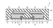
図12は、第4実施形態による半導体装置4の構成例を示す断面図である。第4実施形態では、メモリチップ30上にさらに他のメモリチップ(第3半導体チップ)35が積層されている。第4実施形態のその他の構成は、第1実施形態と同様でよい。
(Fourth embodiment)
FIG. 12 is a cross-sectional view illustrating a configuration example of the semiconductor device 4 according to the fourth embodiment. In the fourth embodiment, another memory chip (third semiconductor chip) 35 is stacked on the
このように、メモリチップ30上にメモリチップ35を積層しても構わない。ただし、メモリチップ35の裏面は、突出部31および凹部32を有さず、平坦である。また、メモリチップ30上に積層するメモリチップ35の数は、特に限定しない。第4実施形態のように、メモリチップ30上に他のメモリチップ35を積層しても、本実施形態の効果は失われない。
As described above, the
(第5実施形態)
図13(A)および図13(B)は、第5実施形態による半導体装置5の構成例を示す断面図および平面図である。尚、図13(B)の平面図において、コントローラチップ20はその概略的な位置のみ示しており、金属ワイヤ60等についての図示は省略している。
(Fifth embodiment)
FIGS. 13A and 13B are a cross-sectional view and a plan view illustrating a configuration example of the
第5実施形態では、メモリチップ30は、その裏面F2に複数の第1領域R1を有し、第1領域R1のそれぞれに突出部31が設けられている。これにより、図1(A)に示すように、メモリチップ30の裏面F2は、樹脂基板10の表面に対する垂直断面において、略U形状に成形されている。メモリチップ30は、コントローラチップ20の上方を亘って跨ぐように設けられており、コントローラチップ20の両側において突出部31が樹脂基板10に接着層50で接着される。コントローラチップ20は、2つの突出部31間に配置され、その上方には、凹部32が配置される。凹部32は、コントローラチップ20の表面上方を被覆している。このように、メモリチップ30は、左右に分離されておらず、一体型のチップであってもよい。メモリチップ30が一体型の場合、メモリチップ30の機械的強度および安定性が向上する。よって、メモリチップ30の湾曲が抑制され、メモリチップ35の積層数を増大させることができる。
In the fifth embodiment, the
半導体装置5は、半導体ウェハ100のトリム処理の位置を変更すれば、第1実施形態の半導体装置1と同様に形成することができる。例えば、第1実施形態の図4(A)において、第2領域R2の凹部32は、隣接するダイシングラインDL間に形成すればよい。尚、トリムブレードTBの幅は、各メモリチップ30の幅よりも小さいものとする。これにより、半導体チップの中心部に凹部32が形成され、凹部32の両側に2つの突出部31が形成される。ダイシングラインDLは、突出部31の中間位置に対応する。従って、ダイシング後、各半導体チップは、その中心部に凹部32を有し、凹部32の両側に2つの突出部31を有する略U形状に形成される。上記変形例1についても、同様に、半導体ウェハ100のトリム処理の位置を変更すれば、半導体装置5を製造することができる。
The
半導体装置5の製造方法として、以下のような製造方法もある。
As a method of manufacturing the
図14(A)および図14(B)は、第5実施形態による半導体装置5の製造方法を示す断面図である。例えば、図2(A)〜図3(A)を参照して説明した工程を経た後、トリムブレードを用いて、図14(A)に示すように、ダイシングラインDL間の半導体チップの中心部に凹部32を形成する。
14A and 14B are cross-sectional views illustrating the method for manufacturing the
次に、CMP法を用いて、半導体ウェハ100の裏面F2を研磨する。このとき、半導体ウェハ100の裏面F2の突出部31が所望の高さになるまで裏面F2を研磨する。これにより、図14(B)に示すように、凹部32の両側に2つの突出部31が形成される。
Next, the back surface F2 of the
その後、図4(B)〜図7を参照して説明した工程を経て、半導体ウェハ100をダイシングする。これにより、図13(A)に示すようなメモリチップ30が形成される。このように、凹部32を形成してから裏面F2を研磨してもよい。
Thereafter, the
(第6実施形態)
図15は、第6実施形態による半導体装置6の構成例を示す断面図である。第6実施形態では、メモリチップ30上にさらに他のメモリチップ(第3半導体チップ)35が積層されている。第6実施形態のその他の構成は、第5実施形態と同様でよい。
(Sixth embodiment)
FIG. 15 is a cross-sectional view illustrating a configuration example of the semiconductor device 6 according to the sixth embodiment. In the sixth embodiment, another memory chip (third semiconductor chip) 35 is stacked on the
このように、メモリチップ30上に他のメモリチップ35を積層しても構わない。ただし、メモリチップ35の裏面は、突出部31および凹部32を有さず、平坦である。また、メモリチップ30上に積層するメモリチップ35の数は、特に限定しない。第6実施形態のように、メモリチップ30上に他のメモリチップ35を積層しても、本実施形態の効果は失われない。
In this manner, another
(第7実施形態)
図16は、第7実施形態による半導体装置7の構成例を示す断面図である。第7実施形態では、メモリチップ30の裏面F2と樹脂基板10との間の全体に接着層50が設けられている。即ち、接着層50は、突出部31と樹脂基板10との間だけでなく、凹部32とコントローラチップ20または樹脂基板10との間にも設けられている。第7実施形態のその他の構成は、第5実施形態と同様でよい。
(Seventh embodiment)
FIG. 16 is a cross-sectional view illustrating a configuration example of the
このように、接着層50がメモリチップ30の下に満たされていれば、接着層50がコントローラチップ20の全体を被覆するので、コントローラチップ20には、略均一な応力が印加される。従って、第7実施形態は、コントローラチップ20がフリップチップ型ではない場合であっても適用することができる。
As described above, when the
第7実施形態は、第6実施形態と組み合わせてもよい。 The seventh embodiment may be combined with the sixth embodiment.
本発明のいくつかの実施形態を説明したが、これらの実施形態は、例として提示したものであり、発明の範囲を限定することは意図していない。これら実施形態は、その他の様々な形態で実施されることが可能であり、発明の要旨を逸脱しない範囲で、種々の省略、置き換え、変更を行うことができる。これら実施形態やその変形は、発明の範囲や要旨に含まれると同様に、特許請求の範囲に記載された発明とその均等の範囲に含まれるものである。 Although several embodiments of the present invention have been described, these embodiments are provided by way of example and are not intended to limit the scope of the invention. These embodiments can be implemented in other various forms, and various omissions, replacements, and changes can be made without departing from the spirit of the invention. These embodiments and their modifications are included in the scope and gist of the invention, and are also included in the invention described in the claims and equivalents thereof.
1〜7 半導体装置、10 樹脂基板、20 コントローラチップ、30 メモリチップ、31 突出部、32 凹部、40、50接着層、60、70 金属ワイヤ、80モールド樹脂 1 to 7 semiconductor device, 10 resin substrate, 20 controller chip, 30 memory chip, 31 protrusion, 32 recess, 40, 50 adhesive layer, 60, 70 metal wire, 80 mold resin
Claims (8)
前記基板の表面上に設けられた第1半導体チップと、
裏面の第1領域において突出している突出部を有する第2半導体チップであって、前記突出部を前記基板の表面に接着させたときに、前記第1領域以外の前記裏面の第2領域が前記第1半導体チップまたは該第1半導体チップと前記基板との間を接続するワイヤの少なくとも一部分の上方に該第1半導体チップに接することなく配置される第2半導体チップと、
前記第1領域と前記基板との間および前記第2領域と前記基板との間に設けられた接着層と、
前記基板上に設けられ、前記第1および第2半導体チップを被覆する樹脂層とを備えた半導体装置。 Board and
A first semiconductor chip provided on a surface of the substrate;
A second semiconductor chip having a protruding portion protruding in a first region on a back surface, wherein when the protruding portion is adhered to a surface of the substrate, the second region on the back surface other than the first region is the second semiconductor chip. A second semiconductor chip disposed above at least a portion of a first semiconductor chip or a wire connecting the first semiconductor chip and the substrate without contacting the first semiconductor chip;
An adhesive layer provided between the first region and the substrate and between the second region and the substrate;
And a resin layer provided on the substrate and covering the first and second semiconductor chips.
前記接着層は、前記第2半導体チップから前記第1方向へ延伸する前記第2領域と前記基板との間、並びに、前記第2半導体チップから前記第2方向へ延伸する前記第2領域と前記基板との間に設けられている、請求項1または請求項2に記載の半導体装置。 In a cross section cut in the arrangement direction of the first and second semiconductor chips, the second region includes a first direction from the second semiconductor chip toward the first semiconductor chip and an opposite side to the first direction. Stretching in both the second direction,
The adhesive layer is provided between the second region extending from the second semiconductor chip in the first direction and the substrate, and the second region extending from the second semiconductor chip in the second direction. The semiconductor device according to claim 1, wherein the semiconductor device is provided between the semiconductor device and a substrate.
複数の前記第2半導体チップ間には、前記樹脂層が設けられている、請求項1から請求項5のいずれか一項に記載の半導体装置。 A plurality of the second semiconductor chips are provided separately on both sides of the first semiconductor chip;
The semiconductor device according to claim 1, wherein the resin layer is provided between the plurality of second semiconductor chips.
前記第1半導体チップは、前記複数の第1領域間に配置されている、請求項1から請求項5のいずれか一項に記載の半導体装置。 The second semiconductor chip has a plurality of the first regions, and is provided over the first semiconductor chip;
The semiconductor device according to claim 1, wherein the first semiconductor chip is disposed between the plurality of first regions.
前記半導体ウェハの凹部を埋め込むように該裏面に接着層を設け、
前記半導体ウェハから個片化された第2半導体チップの前記突出部を基板の表面に前記接着層で接着するとともに、前記第2半導体チップの前記凹部を、該第2半導体チップの下に設けられた第1半導体チップまたは該第1半導体チップと前記基板との間を接続するワイヤの上方に配置し、
前記基板上の前記第1および第2半導体チップを樹脂層で被覆すること、を具備した半導体装置の製造方法。 Cutting a part of the back surface of the semiconductor wafer to form a protrusion projecting in a first region of the back surface and a concave portion recessed in a second region of the back surface other than the first region;
Providing an adhesive layer on the back surface so as to fill the concave portion of the semiconductor wafer,
The projecting portion of the second semiconductor chip singulated from the semiconductor wafer is adhered to the surface of a substrate with the adhesive layer, and the concave portion of the second semiconductor chip is provided below the second semiconductor chip. Placed above the first semiconductor chip or the wire connecting between the first semiconductor chip and the substrate,
A method of manufacturing a semiconductor device, comprising: covering the first and second semiconductor chips on the substrate with a resin layer.
Priority Applications (4)
| Application Number | Priority Date | Filing Date | Title |
|---|---|---|---|
| JP2018146821A JP2020021908A (en) | 2018-08-03 | 2018-08-03 | Semiconductor device and method for manufacturing the same |
| CN201811599371.0A CN110797334B (en) | 2018-08-03 | 2018-12-26 | Semiconductor device and manufacturing method thereof |
| TW107147241A TWI720394B (en) | 2018-08-03 | 2018-12-26 | Semiconductor device and manufacturing method thereof |
| US16/290,488 US10964681B2 (en) | 2018-08-03 | 2019-03-01 | Semiconductor device and method for manufacturing the same |
Applications Claiming Priority (1)
| Application Number | Priority Date | Filing Date | Title |
|---|---|---|---|
| JP2018146821A JP2020021908A (en) | 2018-08-03 | 2018-08-03 | Semiconductor device and method for manufacturing the same |
Publications (1)
| Publication Number | Publication Date |
|---|---|
| JP2020021908A true JP2020021908A (en) | 2020-02-06 |
Family
ID=69228964
Family Applications (1)
| Application Number | Title | Priority Date | Filing Date |
|---|---|---|---|
| JP2018146821A Pending JP2020021908A (en) | 2018-08-03 | 2018-08-03 | Semiconductor device and method for manufacturing the same |
Country Status (4)
| Country | Link |
|---|---|
| US (1) | US10964681B2 (en) |
| JP (1) | JP2020021908A (en) |
| CN (1) | CN110797334B (en) |
| TW (1) | TWI720394B (en) |
Families Citing this family (2)
| Publication number | Priority date | Publication date | Assignee | Title |
|---|---|---|---|---|
| JP2023042073A (en) * | 2021-09-14 | 2023-03-27 | キオクシア株式会社 | Semiconductor device |
| JP2023121355A (en) * | 2022-02-21 | 2023-08-31 | キオクシア株式会社 | Semiconductor device and method for manufacturing semiconductor device |
Family Cites Families (26)
| Publication number | Priority date | Publication date | Assignee | Title |
|---|---|---|---|---|
| AU4242693A (en) * | 1992-05-11 | 1993-12-13 | Nchip, Inc. | Stacked devices for multichip modules |
| US6091138A (en) * | 1998-02-27 | 2000-07-18 | Advanced Micro Devices, Inc. | Multi-chip packaging using bump technology |
| US6294407B1 (en) * | 1998-05-06 | 2001-09-25 | Virtual Integration, Inc. | Microelectronic packages including thin film decal and dielectric adhesive layer having conductive vias therein, and methods of fabricating the same |
| US6351028B1 (en) * | 1999-02-08 | 2002-02-26 | Micron Technology, Inc. | Multiple die stack apparatus employing T-shaped interposer elements |
| JP3913481B2 (en) * | 2001-01-24 | 2007-05-09 | シャープ株式会社 | Semiconductor device and manufacturing method of semiconductor device |
| JP3530158B2 (en) | 2001-08-21 | 2004-05-24 | 沖電気工業株式会社 | Semiconductor device and manufacturing method thereof |
| US20030111720A1 (en) | 2001-12-18 | 2003-06-19 | Tan Lan Chu | Stacked die semiconductor device |
| JP3507059B2 (en) | 2002-06-27 | 2004-03-15 | 沖電気工業株式会社 | Stacked multi-chip package |
| US6906415B2 (en) * | 2002-06-27 | 2005-06-14 | Micron Technology, Inc. | Semiconductor device assemblies and packages including multiple semiconductor devices and methods |
| JP4123027B2 (en) * | 2003-03-31 | 2008-07-23 | セイコーエプソン株式会社 | Manufacturing method of semiconductor device |
| JP4705748B2 (en) | 2003-05-30 | 2011-06-22 | ルネサスエレクトロニクス株式会社 | Manufacturing method of semiconductor device |
| KR100594229B1 (en) * | 2003-09-19 | 2006-07-03 | 삼성전자주식회사 | Semiconductor package and manufacturing method |
| JP3970833B2 (en) | 2003-10-27 | 2007-09-05 | 沖電気工業株式会社 | Semiconductor device, semiconductor device manufacturing method, and semiconductor device inspection method |
| JP3970849B2 (en) | 2004-01-26 | 2007-09-05 | 沖電気工業株式会社 | Semiconductor device, semiconductor device manufacturing method, and semiconductor device inspection method |
| US7242101B2 (en) * | 2004-07-19 | 2007-07-10 | St Assembly Test Services Ltd. | Integrated circuit die with pedestal |
| JP4275113B2 (en) | 2005-07-29 | 2009-06-10 | Okiセミコンダクタ株式会社 | Semiconductor device and manufacturing method thereof |
| RU2422204C2 (en) * | 2006-03-20 | 2011-06-27 | Конинклейке Филипс Электроникс Н.В. | Encased carrier system for electronic micro fluid devices |
| JP2006222470A (en) | 2006-05-29 | 2006-08-24 | Renesas Technology Corp | Semiconductor device and manufacturing method of semiconductor device |
| US20070284139A1 (en) * | 2006-06-10 | 2007-12-13 | Chee Keong Chin | Sawn integrated circuit package system |
| JP2009026843A (en) | 2007-07-18 | 2009-02-05 | Toshiba Corp | Semiconductor device |
| US8841765B2 (en) * | 2011-04-22 | 2014-09-23 | Tessera, Inc. | Multi-chip module with stacked face-down connected dies |
| US8772929B2 (en) * | 2011-11-16 | 2014-07-08 | Taiwan Semiconductor Manufacturing Company, Ltd. | Package for three dimensional integrated circuit |
| JP5918664B2 (en) | 2012-09-10 | 2016-05-18 | 株式会社東芝 | Manufacturing method of stacked semiconductor device |
| TWI517433B (en) | 2013-03-22 | 2016-01-11 | 財團法人工業技術研究院 | Automatically aligned wafer carrier and package structure |
| JP2015176906A (en) * | 2014-03-13 | 2015-10-05 | 株式会社東芝 | Semiconductor device and manufacturing method of semiconductor device |
| JP6586036B2 (en) * | 2016-03-15 | 2019-10-02 | 東芝メモリ株式会社 | Manufacturing method of semiconductor device |
-
2018
- 2018-08-03 JP JP2018146821A patent/JP2020021908A/en active Pending
- 2018-12-26 TW TW107147241A patent/TWI720394B/en active
- 2018-12-26 CN CN201811599371.0A patent/CN110797334B/en active Active
-
2019
- 2019-03-01 US US16/290,488 patent/US10964681B2/en active Active
Also Published As
| Publication number | Publication date |
|---|---|
| TW202008529A (en) | 2020-02-16 |
| US10964681B2 (en) | 2021-03-30 |
| TWI720394B (en) | 2021-03-01 |
| CN110797334B (en) | 2023-10-13 |
| CN110797334A (en) | 2020-02-14 |
| US20200043907A1 (en) | 2020-02-06 |
Similar Documents
| Publication | Publication Date | Title |
|---|---|---|
| US10756060B2 (en) | Semiconductor device | |
| US9583455B2 (en) | Semiconductor device | |
| CN108987358A (en) | Thermal interfacial material with different thickness in packaging part | |
| TWI695492B (en) | Semiconductor device and its manufacturing method | |
| US8785297B2 (en) | Method for encapsulating electronic components on a wafer | |
| JP2020096153A (en) | Semiconductor package structure and manufacturing method of the same | |
| JP2022014121A (en) | Semiconductor device and manufacturing method for the same | |
| US8994161B2 (en) | Semiconductor device package and methods for producing same | |
| JP2002093992A (en) | Semiconductor device and manufacturing method thereof | |
| TW201434096A (en) | Semiconductor device and method of manufacturing same | |
| US10964681B2 (en) | Semiconductor device and method for manufacturing the same | |
| TWI750439B (en) | Semiconductor device and manufacturing method thereof | |
| TWI740350B (en) | Manufacturing method of semiconductor device | |
| JP2022036756A (en) | Semiconductor device | |
| US8105877B2 (en) | Method of fabricating a stacked type chip package structure | |
| US8513820B2 (en) | Package substrate structure and chip package structure and manufacturing process thereof | |
| JP5234703B2 (en) | Manufacturing method of semiconductor device | |
| KR20250033920A (en) | Semiconductor package and method for fabricating the same | |
| JP2004022982A (en) | Stacked semiconductor device | |
| KR20090067610A (en) | Bonding pad of semiconductor device and manufacturing method thereof | |
| CN115249669A (en) | Dual-chip semiconductor package and method of manufacturing the same | |
| JP2012054397A (en) | Semiconductor element, manufacturing method thereof and semiconductor device | |
| JP2006332274A (en) | Semiconductor device and manufacturing method thereof | |
| KR20160149733A (en) | Chip embedded printed circuit board and fabrication method thereof |