JP2020004889A - Substrate cutting method and substrate cutting device - Google Patents
Substrate cutting method and substrate cutting device Download PDFInfo
- Publication number
- JP2020004889A JP2020004889A JP2018124058A JP2018124058A JP2020004889A JP 2020004889 A JP2020004889 A JP 2020004889A JP 2018124058 A JP2018124058 A JP 2018124058A JP 2018124058 A JP2018124058 A JP 2018124058A JP 2020004889 A JP2020004889 A JP 2020004889A
- Authority
- JP
- Japan
- Prior art keywords
- substrate
- laser
- processing
- scribe line
- chamfered portion
- Prior art date
- Legal status (The legal status is an assumption and is not a legal conclusion. Google has not performed a legal analysis and makes no representation as to the accuracy of the status listed.)
- Pending
Links
Images
Classifications
-
- C—CHEMISTRY; METALLURGY
- C03—GLASS; MINERAL OR SLAG WOOL
- C03B—MANUFACTURE, SHAPING, OR SUPPLEMENTARY PROCESSES
- C03B33/00—Severing cooled glass
- C03B33/02—Cutting or splitting sheet glass or ribbons; Apparatus or machines therefor
- C03B33/0222—Scoring using a focussed radiation beam, e.g. laser
-
- C—CHEMISTRY; METALLURGY
- C03—GLASS; MINERAL OR SLAG WOOL
- C03B—MANUFACTURE, SHAPING, OR SUPPLEMENTARY PROCESSES
- C03B33/00—Severing cooled glass
- C03B33/02—Cutting or splitting sheet glass or ribbons; Apparatus or machines therefor
- C03B33/023—Cutting or splitting sheet glass or ribbons; Apparatus or machines therefor the sheet or ribbon being in a horizontal position
- C03B33/033—Apparatus for opening score lines in glass sheets
-
- C—CHEMISTRY; METALLURGY
- C03—GLASS; MINERAL OR SLAG WOOL
- C03B—MANUFACTURE, SHAPING, OR SUPPLEMENTARY PROCESSES
- C03B33/00—Severing cooled glass
- C03B33/02—Cutting or splitting sheet glass or ribbons; Apparatus or machines therefor
- C03B33/023—Cutting or splitting sheet glass or ribbons; Apparatus or machines therefor the sheet or ribbon being in a horizontal position
-
- C—CHEMISTRY; METALLURGY
- C03—GLASS; MINERAL OR SLAG WOOL
- C03B—MANUFACTURE, SHAPING, OR SUPPLEMENTARY PROCESSES
- C03B33/00—Severing cooled glass
- C03B33/07—Cutting armoured, multi-layered, coated or laminated, glass products
-
- C—CHEMISTRY; METALLURGY
- C03—GLASS; MINERAL OR SLAG WOOL
- C03B—MANUFACTURE, SHAPING, OR SUPPLEMENTARY PROCESSES
- C03B33/00—Severing cooled glass
- C03B33/08—Severing cooled glass by fusing, i.e. by melting through the glass
- C03B33/082—Severing cooled glass by fusing, i.e. by melting through the glass using a focussed radiation beam, e.g. laser
-
- C—CHEMISTRY; METALLURGY
- C03—GLASS; MINERAL OR SLAG WOOL
- C03B—MANUFACTURE, SHAPING, OR SUPPLEMENTARY PROCESSES
- C03B33/00—Severing cooled glass
- C03B33/09—Severing cooled glass by thermal shock
- C03B33/091—Severing cooled glass by thermal shock using at least one focussed radiation beam, e.g. laser beam
Landscapes
- Chemical & Material Sciences (AREA)
- Engineering & Computer Science (AREA)
- Materials Engineering (AREA)
- Organic Chemistry (AREA)
- Physics & Mathematics (AREA)
- Health & Medical Sciences (AREA)
- Optics & Photonics (AREA)
- Toxicology (AREA)
- Thermal Sciences (AREA)
- Laser Beam Processing (AREA)
- Re-Forming, After-Treatment, Cutting And Transporting Of Glass Products (AREA)
- Processing Of Stones Or Stones Resemblance Materials (AREA)
- Dicing (AREA)
- Perforating, Stamping-Out Or Severing By Means Other Than Cutting (AREA)
Abstract
Description
本発明は、基板の分断方法及び分断装置に関する。 The present invention relates to a substrate cutting method and a substrate cutting device.
ガラス基板をスクライブ加工する方法として、レーザ加工が知られている。レーザ加工では、例えば、赤外線ピコ秒レーザが用いられている。この場合、レーザがパルスによる内部加工を平面方向に断続的に行って複数のレーザフィラメントを形成することで、スクライブラインを形成する方法が知られている(例えば、特許文献1を参照)。
特許文献1に示す技術では、収束レーザビームは、基板内にフィラメントを作り出すように選択されたエネルギー及びパルス持続時間を有するパルスで構成される。そして、複数のフィラメントによって、スクライブラインが形成される。
As a method for scribing a glass substrate, laser processing is known. In laser processing, for example, an infrared picosecond laser is used. In this case, there is known a method of forming a scribe line by forming a plurality of laser filaments by intermittently performing internal processing by a laser in a planar direction (for example, see Patent Document 1).
In the technique disclosed in US Pat. No. 6,037,097, a focused laser beam is composed of pulses having an energy and a pulse duration selected to create a filament in a substrate. Then, a scribe line is formed by the plurality of filaments.
従来、基板を分断した後に、基板の端面において角部を取り去る面取り加工が行われている。
しかし、基板の分断後に面取り加工を行うと、基板の分断と面取り加工の両方が必要になるので、作業工程が増加する。
2. Description of the Related Art Conventionally, a chamfering process for removing a corner at an end face of a substrate after dividing the substrate has been performed.
However, if the chamfering is performed after the substrate is divided, both the dividing and the chamfering of the substrate are required, so that the number of working steps increases.
本発明の目的は、基板の加工方法において、少ない作業工程によって、基板の端面に面取りを形成することにある。 An object of the present invention is to form a chamfer on an end face of a substrate with a small number of working steps in a method for processing a substrate.
以下に、課題を解決するための手段として複数の態様を説明する。これら態様は、必要に応じて任意に組み合せることができる。 Hereinafter, a plurality of modes will be described as means for solving the problems. These embodiments can be arbitrarily combined as needed.
本発明の一見地に係る基板の分断方法は、下記のステップを備えている。
◎空間光位相変調を用いて、基板に対して外側面から延びる面取り部を含む複数の加工痕を、平面方向に連続して形成することでスクライブラインを形成するレーザ光照射ステップ
◎基板に力を加えることで、スクライブラインに沿って基板を分断する分断ステップ
この分断方法では、基板が分断されると、残った基板の端面には面取り部が形成されている。したがって、少ない作業工程によって、基板の端面に面取りを形成できる。
なお、面取り部とは、例えば、C面(隅切り、コーナーカット)、R面、逆R面、エグリ、切り欠き等が形成された部分である。
A method for cutting a substrate according to an aspect of the present invention includes the following steps.
◎ Laser beam irradiation step of forming a scribe line by continuously forming a plurality of processing marks including a chamfered portion extending from the outer surface with respect to the substrate in a planar direction using spatial light phase modulation ◎ In the dividing method, when the substrate is divided, a chamfered portion is formed on an end surface of the remaining substrate. Therefore, the chamfer can be formed on the end face of the substrate with a small number of operation steps.
The chamfered portion is, for example, a portion where a C surface (corner cut, corner cut), an R surface, an inverted R surface, an edge, a notch, and the like are formed.
レーザ光照射ステップは、下記のステップを有していてもよい。
◎複数の加工痕を、面取り部が作成される位置において平面方向に間隔を空けて形成する第1ステップ
◎複数の加工痕を、面取り部が作成される位置において、先に形成された複数の加工痕の平面方向間に形成する第2ステップ
The laser beam irradiation step may include the following steps.
◎ First step of forming a plurality of processing marks at intervals in the plane direction at a position where a chamfered part is formed ◎ A plurality of processing marks formed first at a position where a chamfered part is formed Second step of forming between processing marks in the plane direction
第1ステップでは、加工痕同士の間隔は、独立した加工痕同士の間に形成されてもよいし、複数の加工痕の集まり同士の間に形成されてもよい。
この分断方法では、複数の加工痕を少なくとも2回に分けて形成することで面取り部を形成しているので、レーザ光照射パルスの強度を低くしても、加工痕を連続して形成することで面取り部を加工できる。そのため、面取り部において加工痕が例えば上下方向に極端に長くなることがなく、したがって面取り部の形状が滑らかになる。
In the first step, the interval between the processing marks may be formed between independent processing marks or between a group of a plurality of processing marks.
In this dividing method, since the chamfered portion is formed by forming a plurality of processing marks at least twice, the processing marks can be formed continuously even if the intensity of the laser beam irradiation pulse is reduced. The chamfer can be machined. For this reason, the processing mark in the chamfered portion does not become extremely long in the vertical direction, for example, and the shape of the chamfered portion becomes smooth.
本発明の他の見地に係る基板の分断装置は、レーザ装置と、基板分断装置と、を備えている。
レーザ装置は、空間光位相変調を用いて、基板に対して外側面から延びる面取り部を含む複数の加工痕を、平面方向に連続して形成することでスクライブラインを形成するレーザ光照射ステップを実行する。
基板分断装置は、基板に力を加えることで、スクライブラインに沿って基板を分断する分断ステップを実行する。
この分断装置では、基板が分断されると、残った基板の端面には面取り部が形成されている。したがって、少ない作業工程によって、基板の端面に面取りを形成できる。
A substrate cutting device according to another aspect of the present invention includes a laser device and a substrate cutting device.
The laser device performs a laser beam irradiation step of forming a scribe line by continuously forming a plurality of processing marks including a chamfered portion extending from an outer surface with respect to the substrate in a planar direction using spatial light phase modulation. Execute.
The substrate cutting device executes a cutting step of cutting the substrate along a scribe line by applying a force to the substrate.
In this cutting device, when the substrate is cut, a chamfered portion is formed on an end surface of the remaining substrate. Therefore, the chamfer can be formed on the end face of the substrate with a small number of operation steps.
本発明に係る基板の分断方法及び分断装置では、少ない作業工程によって、基板の端面に面取りを形成できる。 ADVANTAGE OF THE INVENTION In the cutting method and apparatus of the board | substrate which concern on this invention, a chamfer can be formed in the end surface of a board | substrate with few working steps.
1.第1実施形態
(1)全体構成
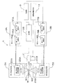
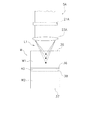
図1及び図2を用いて、レーザ加工装置1の全体構成を説明する。図1は、第1実施形態のレーザ加工装置の模式図である。図2は、空間光位相変調器の模式的動作説明図である。
1. First Embodiment (1) Overall Configuration The overall configuration of a
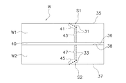
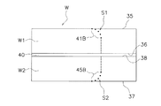
レーザ加工装置1は、貼り合わせ基板W(以下、「基板W」)にスクライブラインを形成する装置である。基板Wは、第1基板W1と、第2基板W2とを有している。基板Wは、例えば、液晶ガラス基板である。
図2に示すように、第1基板W1と第2基板W2は、シール材40によって貼り合わされている。第1基板W1は外側面35と内側面36を有している。第2基板W2は外側面37と内側面38とを有している。内側面36と内側面38の間にシール材40が配置されている。
The
As shown in FIG. 2, the first substrate W1 and the second substrate W2 are bonded together by a
レーザ加工装置1は、第1レーザ装置3Aを有している。第1レーザ装置3Aは、第1基板W1に第1スクライブラインS1(図3)を形成する装置である。
The
第1レーザ装置3Aは、第1レーザ発振器15Aと、第1レーザ制御部17Aとを有している。第1レーザ発振器15Aは、例えば、波長340〜1100nmのピコ秒レーザである。第1レーザ制御部17Aは、第1レーザ発振器15Aの駆動及びレーザパワーを制御できる。
レーザ加工装置1は、第1伝送光学系5Aを有している。第1伝送光学系5Aは、第1レーザ装置3Aから出射されたレーザ光を変調する第1空間光位相変調器21Aを有している。第1空間光位相変調器21Aは、例えば透過型であり、透過型の空間光移送変調器(SLM:Spatial Light Modulator)であってもよい。また透過型の空間光移送変調器に代えて反射型液晶(LCOS:Liquid Crystal on Silicon)の空間光位相変調器などの反射型の空間光移送変調器を使用してもよい。第1空間光位相変調器21Aは、レーザ光を変調すると共に、下方に第1レーザL1を照射する。第1伝送光学系5Aは、第1空間光位相変調器21Aの下方に、第1集光レンズ23Aを有している。
The first laser device 3A has a
The
レーザ加工装置1は、第2レーザ装置3Bを備えている。第2レーザ装置3Bは、第2基板W2に第2スクライブラインS2(図3)を形成する装置である。
第2レーザ装置3Bは、第2レーザ発振器15Bと、第2レーザ制御部17Bとを有している。第2レーザ発振器15Bは、例えば、波長340〜1100nmのピコ秒レーザである。第2レーザ制御部17Bは第2レーザ発振器15Bの駆動及びレーザパワーを制御できる。
レーザ加工装置1は、第2伝送光学系5Bを有している。第2伝送光学系5Bは、第2レーザ装置3Bから出射されたレーザ光を変調する第2空間光位相変調器21Bを有している。第2空間光位相変調器21Bは、第1空間光位相変調器21Aと同じく、SLMであってもよい。第2空間光位相変調器21Bは、レーザ光を変調すると共に、上方に第2レーザ光L2を照射する。第2伝送光学系5Bは、第2空間光位相変調器21Bの上方に、第2集光レンズ23Bを有している。
The
The second laser device 3B has a
The
レーザ加工装置1は、駆動部25を有している。駆動部25は、第1空間光位相変調器21A及び第2空間光位相変調器21Bにおける各画素電極に所定電圧を印加し、液晶層に所定の変調パターンを表示させ、これにより、レーザ光を第1空間光位相変調器21A及び第2空間光位相変調器21Bで所望に変調させる。ここで、液晶層に表示される変調パターンは、例えば、加工痕を形成しようとする位置、照射するレーザ光の波長、加工対象物の材料、及び第1伝送光学系5A及び第2伝送光学系5Bや加工対象物の屈折率等に基づいて予め導出され、制御部9に記憶されている。
この結果、図2に示すように、第1空間光位相変調器21A及び第2空間光位相変調器21Bは、任意の多数のビームを形成することができ、多数のビームによる同時加工が可能になる。
The
As a result, as shown in FIG. 2, the first spatial
レーザ加工装置1は、基板Wを保持して駆動する駆動装置7を有している。駆動装置7は、駆動装置操作部13によって移動される。駆動装置操作部13は、駆動装置7を水平方向に移動させる。
The
レーザ加工装置1は、制御部9を備えている。制御部9は、プロセッサ(例えば、CPU)と、記憶装置(例えば、ROM、RAM、HDD、SSDなど)と、各種インターフェース(例えば、A/Dコンバータ、D/Aコンバータ、通信インターフェースなど)を有するコンピュータシステムである。制御部9は、記憶部(記憶装置の記憶領域の一部又は全部に対応)に保存されたプログラムを実行することで、各種制御動作を行う。
制御部9は、単一のプロセッサで構成されていてもよいが、各制御のために独立した複数のプロセッサから構成されていてもよい。
The
The
制御部9は、第1レーザ制御部17A及び第2レーザ制御部17Bを制御できる。制御部9は、駆動部25を制御できる。制御部9は、駆動装置操作部13を制御できる。
制御部9には、図示しないが、基板Wの大きさ、形状及び位置を検出するセンサ、各装置の状態を検出するためのセンサ及びスイッチ、並びに情報入力装置が接続されている。
The
Although not shown, a sensor for detecting the size, shape and position of the substrate W, sensors and switches for detecting the state of each device, and an information input device are connected to the
(2)スクライブ加工方法
図3を用いて、レーザ加工装置1によるスクライブ加工方法を説明する。図3は、スクライブライン形成工程における基板の模式的断面である。
(2) Scribing Method A scribing method using the
(2−1)第1レーザ光照射ステップ
第1基板W1側から第1レーザ光L1を照射することで、第1スクライブラインS1を形成する。具体的には、第1基板W1内部に光軸に沿って形成された複数の第1加工痕31が、平面方向に(紙面直交方向に)連続して形成される。第1加工痕31の厚み方向の形成位置は、第1基板W1の外側面35と内側面36との間である。
(2-1) First Laser Light Irradiation Step The first scribe line S1 is formed by irradiating the first laser light L1 from the first substrate W1 side. Specifically, a plurality of first processing traces 31 formed along the optical axis inside the first substrate W1 are continuously formed in a plane direction (in a direction orthogonal to the paper surface). The formation position of the
第1スクライブラインS1の第1加工痕31は、第1基板W1に対して外側面35から延びる面取り部41を有する。第1加工痕31は、さらに、面取り部41から内側面36に向かって延びる直線部43を有する。面取り部41は、断面直線状であり、他面の外側面35側の角を落とす形状である。
この実施形態では、第1スクライブラインのS1の平面視の1箇所では、複数の第1加工痕31は厚み方向に同時に形成される。
なお、第1加工痕31のうち面取り部41を構成するものは、直線部43を構成するものに比べて、基板Wの厚さ方向の長さが短い。なぜなら、面取り部41の集光点は、直線部43の集光点よりも集光のNAが大きくなるようにしているからである。この結果、直線部43には基板Wの厚さ方向に長い第1加工痕31が形成され、面取り部41には基板Wの厚さ方向に短い第1加工痕31が形成される。
The
In this embodiment, a plurality of first processing traces 31 are simultaneously formed in the thickness direction at one location of the first scribe line S1 in plan view.
Note that, of the first processing traces 31, those forming the chamfered
(2−2)第2レーザ光照射ステップ
第2基板W2側から第2レーザ光L2を照射することで、第2スクライブラインS2を形成する。具体的には、第2基板W2内部に光軸に沿って形成された複数の第2加工痕33が、第1加工痕31に沿って平面方向に(紙面直交方向に)連続して形成される。
(2-2) Second Laser Light Irradiation Step The second scribe line S2 is formed by irradiating the second laser light L2 from the second substrate W2 side. Specifically, a plurality of second processing marks 33 formed along the optical axis inside the second substrate W2 are formed continuously in a planar direction (in a direction orthogonal to the paper surface) along the first processing marks 31. You.
第2加工痕33の厚み方向の形成位置は、第2基板W2の内側面38と外側面37との間である。
第2スクライブラインS2の第2加工痕33は、第2基板W2に対して外側面37から延びる面取り部45を有する。第2加工痕33は、さらに、面取り部45から内側面38に向かって延びる直線部47を有する。面取り部45は、断面直線状であり、端面の外側面37側の角を落とす形状である。
この実施形態では、第2スクライブラインのS2の平面視の1箇所では、複数の第2加工痕33は厚み方向に同時に形成される。
なお、第2加工痕33のうち面取り部45を構成するものは、直線部47を構成するものに比べて、基板Wの厚さ方向の長さが短い。なぜなら、面取り部45の集光点は、直線部47の集光点よりも集光のNAが大きくなるようにしているからである。この結果、直線部47には基板Wの厚さ方向に長い第2加工痕33が形成され、面取り部41には基板Wの厚さ方向に短い第2加工痕33が形成される。
The formation position of the
The
In this embodiment, at one location of the second scribe line S2 in plan view, the plurality of second processing marks 33 are formed simultaneously in the thickness direction.
Note that, of the second processing traces 33, those forming the chamfered
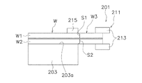
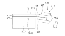
(3)基板分断装置
図4〜図6を用いて、基板分断装置201を説明する。図4及び図5は、基板分断装置の構成及び動作を説明する模式図である。図6は、分断後の基板の模式的断面図である。なお、基板分断装置201は、レーザ加工装置1の制御部9によって制御されてもよいし、他の制御部によって制御されてもよい。
基板分断装置201は、スクライブラインが形成された基板から端材を分割除去することで製品を切り出す装置である。
(3) Board Cutting Apparatus The
The
基板分断装置201は、保持テーブル203を有している。保持テーブル203は、水平な吸着面203aを有しており、そこには加工対象となる基板Wが載置される。保持テーブル203の吸着面203aには、基板Wを安定保持する多数のエア吸着孔(図示せず)が設けられている。
保持テーブル203は、特に、基板Wの製品部分を吸着固定する吸着台である。第2スクライブラインS2が保持テーブル203の縁部に一致するように、基板Wは保持テーブル203に置かれる。
The
The holding table 203 is an adsorption table for adsorbing and fixing the product portion of the substrate W, in particular. The substrate W is placed on the holding table 203 such that the second scribe line S2 coincides with the edge of the holding table 203.
基板分断装置201は、チャック機構211を有している。チャック機構211は、保持テーブル203の吸着面203aからはみ出した基板Wの一端である端材W3を掴むように把持する装置である。
チャック機構211は、チャック部材213を有している。チャック部材213は、開閉自在に構成されている。
チャック機構211は、チャック部材213を駆動するための把持動作機構(図示せず)を有している。
基板分断装置201は、基板Wの製品部分(第1及び第2スクライブラインS1、S2を挟んで端材W3と反対側の部分)を上側から押さえて固定するための押圧機構215をさらに有している。
The
The
The
The
基板分断装置201は、回動機構(図示せず)を有している。回動機構は、チャック部材213が紙面直交方向に延びる軸を支点として所定角度だけ回動できるように、チャック部材213を保持している。回動機構は、例えば、回転モータを有している。
基板分断装置201は、昇降機構(図示せず)を有している。昇降機構は、チャック部材213及び回動機構を昇降させるための装置である。昇降機構は、例えば、圧力シリンダを有している。
The
The
基板分断装置201は、図4に示すように、チャック部材213によって端材W3を把持する。
次に、基板分断装置201は、図5に示すように、チャック部材213を昇降して傾けることで、端材W3を製品から切り離す。このとき、押圧機構215は、基板Wの製品部分を保持テーブル203との間で挟むことで、その部分を保持テーブル203から浮かないようにしている。
なお、チャック部材213は、一方向に傾けた後に、逆方向に傾けてもよい。これにより、分断がより確実に行われる。
この結果、第1基板W1の第1スクライブラインS1と第2基板W2の第2スクライブラインS2に沿って、分断が行われる。
As shown in FIG. 4, the
Next, as shown in FIG. 5, the
Note that the
As a result, the cutting is performed along the first scribe line S1 of the first substrate W1 and the second scribe line S2 of the second substrate W2.
この結果、図6に示すように、基板Wが分断されると、残った基板Wの端面には面取り部41、45が形成されている。つまり、分断と共に面取りが実現される。したがって、少ない作業工程によって、基板Wの端面に面取り部41、45を形成できる。
As a result, as shown in FIG. 6, when the substrate W is cut, chamfers 41 and 45 are formed on the end surface of the remaining substrate W. That is, chamfering is realized together with division. Therefore, the chamfered
2.第2実施形態
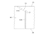
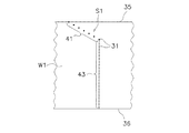
第1実施形態では、複数の加工痕は平面視の1箇所において基板の厚み方向に同時に形成されていたが、複数回に分けて加工痕を形成してもよい。図7及び図8を用いて、そのような実施形態を説明する。図7及び図8は、第2実施形態のスクライブライン形成工程における基板の模式的断面である。
2. Second Embodiment In the first embodiment, a plurality of processing marks are simultaneously formed in one direction in a plan view in the thickness direction of the substrate, but the processing marks may be formed in a plurality of times. Such an embodiment will be described with reference to FIGS. 7 and 8 are schematic cross sections of a substrate in a scribe line forming step according to the second embodiment.
以下、第1基板の第1スクライブラインS1の形成を説明する。
最初に、図7に示すように、直線部作成位置43Aに第1加工痕31が形成される。このとき、同時に、面取り部作成位置41Aにおいて例えば最終的な第1加工痕31に対して一つおきに第1加工痕31が形成される。つまり、複数の第1加工痕31が、面取り部作成位置41Aにおいて平面方向に間隔を空けて形成される。
次に、図8に示すように、複数の第1加工痕31が、面取り部作成位置41Aにおいて、先に形成された複数の第1加工痕31の平面方向間に形成される。具体的には、1つずつ独立して形成された第1加工痕31の間に、1つの第1加工痕31が形成される。
Hereinafter, formation of the first scribe line S1 of the first substrate will be described.
First, as shown in FIG. 7, the first processing traces 31 are formed at the linear
Next, as shown in FIG. 8, a plurality of first processing traces 31 are formed between the plurality of first processing traces 31 previously formed in the plane direction at the chamfered
この実施形態では、複数の第1加工痕31を少なくとも2回に分けて形成することで面取り部41を形成しているので、レーザ光照射パルスの強度を低くしても、第1加工痕31を連続して形成することで面取り部41を加工できる。そのため、面取り部41において第1加工痕31が例えば上下方向に極端に長くなることがなく、したがって面取り部41の形状が滑らかになる。
なお、前記実施形態では面取り部作成位置41Aにおける第1ステップでは第1加工痕31は1つずつ独立して形成されていたが、複数の第1加工痕31同士が連続して形成されたグループが複数形成されてもよい。
In this embodiment, since the chamfered
In the above-described embodiment, in the first step at the chamfered
3.第3実施形態
第1実施形態及び第2実施形態では面取り部はC面であったが、他の形状であってもよい。図9を用いて、そのような実施形態を説明する。図9は、第3実施形態のスクライブブライン形成工程における基板の模式的断面である。
図9に示すように、R面の面取り部にも第1実施形態及び第2実施形態のレーザ光照射によるスクライブライン形成を適用できる。
3. Third Embodiment In the first embodiment and the second embodiment, the chamfered portion is the C-plane, but may have another shape. Such an embodiment will be described with reference to FIG. FIG. 9 is a schematic cross section of a substrate in a scribe brine forming step of the third embodiment.
As shown in FIG. 9, the scribe line formation by laser beam irradiation of the first and second embodiments can be applied to the chamfered portion of the R surface.
4.他の実施形態
以上、本発明の複数の実施形態について説明したが、本発明は上記実施形態に限定されるものではなく、発明の要旨を逸脱しない範囲で種々の変更が可能である。特に、本明細書に書かれた複数の実施形態及び変形例は必要に応じて任意に組み合せ可能である。
基板は、ガラス、半導体ウェハ、セラミックス等の脆性材料基板であればよく、特に限定されない。
貼り合わせ基板以外の基板にも本発明を適用できる。
前記実施形態では基板分断装置は基板の端材を除去する装置であったが、他の基板分断装置であってもよい。
4. Other Embodiments A plurality of embodiments of the present invention have been described above, but the present invention is not limited to the above embodiments, and various changes can be made without departing from the spirit of the invention. In particular, a plurality of embodiments and modifications described in this specification can be arbitrarily combined as needed.
The substrate is not particularly limited as long as it is a substrate made of a brittle material such as glass, a semiconductor wafer, and ceramics.
The present invention can be applied to substrates other than the bonded substrate.
In the above-described embodiment, the substrate cutting device is a device for removing offcuts of the substrate, but may be another substrate cutting device.
本発明は、レーザ装置を用いたパルスによる基板の内部加工を平面方向に断続的に行うことでスクライブラインを形成する方法及び装置に広く適用できる。 INDUSTRIAL APPLICATION This invention can be widely applied to the method and apparatus which form a scribe line by performing internal processing of a board | substrate by the pulse using a laser apparatus intermittently in a plane direction.
1 :レーザ加工装置
3A :第1レーザ装置
3B :第2レーザ装置
5A :第1伝送光学系
5B :第2伝送光学系
7 :駆動装置
9 :制御部
11 :チャック機構
13 :駆動装置操作部
15A :第1レーザ発振器
15B :第2レーザ発振器
17A :第1レーザ制御部
17B :第2レーザ制御部
21A :第1空間光位相変調器
21B :第2空間光位相変調器
23A :第1集光レンズ
23B :第2集光レンズ
25 :駆動部
31 :第1加工痕
33 :第2加工痕
35 :外側面
36 :内側面
37 :外側面
38 :内側面
40 :シール材
41 :面取り部
41A :面取り部作成位置
43 :直線部
43A :直線部作成位置
45 :面取り部
47 :直線部
S1 :第1スクライブライン
S2 :第2スクライブライン
W :貼り合わせ基板
W1 :第1基板
W2 :第2基板
W3 :端材
1: laser processing device 3A: first laser device 3B:
Claims (3)
空間光位相変調を用いて、基板に対して外側面から延びる面取り部を含む複数の加工痕を、平面方向に連続して形成することでスクライブラインを形成するレーザ光照射ステップと、
前記基板に力を加えることで、前記スクライブラインに沿って前記基板を分断する分断ステップと、
を備えた基板の分断方法。 A method of dividing a substrate,
Using spatial light phase modulation, a plurality of processing marks including a chamfer extending from the outer surface with respect to the substrate, a laser beam irradiation step of forming a scribe line by continuously forming in a planar direction,
By applying a force to the substrate, a dividing step of dividing the substrate along the scribe line,
A method for cutting a substrate comprising:
前記複数の加工痕を、前記面取り部が作成される位置において平面方向に間隔を空けて形成する第1ステップと、
前記複数の加工痕を、前記面取り部が作成される位置において先に形成された複数の加工痕の平面方向間に形成する第2ステップと、を有する、請求項1に記載の基板の分断方法。 The laser light irradiation step,
A first step of forming the plurality of processing traces at intervals in a plane direction at a position where the chamfered portion is created;
2. The method according to claim 1, further comprising: forming a plurality of processing marks in a plane direction of the plurality of processing marks previously formed at a position where the chamfered portion is formed. .
空間光位相変調を用いて、基板に対して外側面から延びる面取り部を含む複数の加工痕を、平面方向に連続して形成することでスクライブラインを形成するレーザ光照射ステップを実行するレーザ装置と、
前記基板に力を加えることで、前記スクライブラインに沿って前記基板を分断する分断ステップを実行する基板分断装置と、
を備えた基板の分断装置。 A substrate cutting device,
A laser device that executes a laser beam irradiation step of forming a scribe line by continuously forming a plurality of processing marks including a chamfered portion extending from an outer surface with respect to a substrate in a planar direction using spatial light phase modulation. When,
By applying a force to the substrate, a substrate cutting device that executes a cutting step of cutting the substrate along the scribe line,
A substrate cutting device provided with:
Priority Applications (4)
| Application Number | Priority Date | Filing Date | Title |
|---|---|---|---|
| JP2018124058A JP2020004889A (en) | 2018-06-29 | 2018-06-29 | Substrate cutting method and substrate cutting device |
| KR1020190075717A KR20200002634A (en) | 2018-06-29 | 2019-06-25 | Method and apparatus for dividing substrate |
| TW108122486A TW202015114A (en) | 2018-06-29 | 2019-06-27 | Dividing method and dividing device of substrate can form a chamfer on an end surface of a substrate through a less number of working steps |
| CN201910567292.XA CN110655316A (en) | 2018-06-29 | 2019-06-27 | Substrate dividing method and dividing device |
Applications Claiming Priority (1)
| Application Number | Priority Date | Filing Date | Title |
|---|---|---|---|
| JP2018124058A JP2020004889A (en) | 2018-06-29 | 2018-06-29 | Substrate cutting method and substrate cutting device |
Publications (1)
| Publication Number | Publication Date |
|---|---|
| JP2020004889A true JP2020004889A (en) | 2020-01-09 |
Family
ID=69028648
Family Applications (1)
| Application Number | Title | Priority Date | Filing Date |
|---|---|---|---|
| JP2018124058A Pending JP2020004889A (en) | 2018-06-29 | 2018-06-29 | Substrate cutting method and substrate cutting device |
Country Status (4)
| Country | Link |
|---|---|
| JP (1) | JP2020004889A (en) |
| KR (1) | KR20200002634A (en) |
| CN (1) | CN110655316A (en) |
| TW (1) | TW202015114A (en) |
Cited By (11)
| Publication number | Priority date | Publication date | Assignee | Title |
|---|---|---|---|---|
| US20220193821A1 (en) * | 2020-12-21 | 2022-06-23 | Seagate Technology Llc | Structured discrete beam formation for cutting transparent substrates |
| CN115026412A (en) * | 2021-02-25 | 2022-09-09 | 深圳市大族半导体装备科技有限公司 | Laser processing device and method for brittle product |
| WO2023012210A1 (en) | 2021-08-04 | 2023-02-09 | Trumpf Laser- Und Systemtechnik Gmbh | Method and apparatus for laser processing of a workpiece |
| DE102021123962A1 (en) | 2021-09-16 | 2023-03-16 | Trumpf Laser- Und Systemtechnik Gmbh | Method and device for laser machining a workpiece |
| WO2023088912A1 (en) | 2021-11-18 | 2023-05-25 | Trumpf Laser- Und Systemtechnik Gmbh | Method for the laser processing of a workpiece |
| CN116867598A (en) * | 2021-02-02 | 2023-10-10 | 通快激光与系统工程有限公司 | Apparatus and method for laser machining a workpiece |
| WO2023209034A1 (en) | 2022-04-28 | 2023-11-02 | Trumpf Laser- Und Systemtechnik Gmbh | Method for separating a workpiece |
| JP2024504842A (en) * | 2021-02-02 | 2024-02-01 | トルンプフ レーザー- ウント ジュステームテヒニク ゲゼルシャフト ミット ベシュレンクテル ハフツング | Apparatus and method for laser processing workpieces |
| JP2024516808A (en) * | 2021-04-23 | 2024-04-17 | ショット アクチエンゲゼルシャフト | Method and substrate for controlling the energy distribution introduced into a substrate using a line focus of a laser beam - Patents.com |
| DE102022130022A1 (en) | 2022-11-14 | 2024-05-16 | Trumpf Laser Gmbh | Method and device for laser processing of a workpiece |
| DE102022131536A1 (en) | 2022-11-29 | 2024-05-29 | Trumpf Laser- Und Systemtechnik Gmbh | Method and laser system for separating a workpiece |
Citations (3)
| Publication number | Priority date | Publication date | Assignee | Title |
|---|---|---|---|---|
| WO2011065373A1 (en) * | 2009-11-25 | 2011-06-03 | 浜松ホトニクス株式会社 | Laser processing method |
| JP2013089714A (en) * | 2011-10-17 | 2013-05-13 | Disco Abrasive Syst Ltd | Chip formation method |
| JP2015226012A (en) * | 2014-05-29 | 2015-12-14 | 浜松ホトニクス株式会社 | Laser processing apparatus and laser processing method |
Family Cites Families (9)
| Publication number | Priority date | Publication date | Assignee | Title |
|---|---|---|---|---|
| CN101610870B (en) * | 2007-10-16 | 2013-09-11 | 三星钻石工业股份有限公司 | U-groove processing method of brittle material substrate and removal processing method, drilling processing method and chamfering method using the method |
| JP5102846B2 (en) * | 2007-12-19 | 2012-12-19 | 三星ダイヤモンド工業株式会社 | Method and apparatus for chamfering a brittle material substrate |
| JP6121901B2 (en) | 2010-07-12 | 2017-04-26 | ロフィン−シナー テクノロジーズ インコーポレーテッド | Material processing by laser filament formation |
| JP5758116B2 (en) * | 2010-12-16 | 2015-08-05 | 株式会社ディスコ | Split method |
| TWI457191B (en) * | 2011-02-04 | 2014-10-21 | Mitsuboshi Diamond Ind Co Ltd | Laser scribing method and laser processing apparatus |
| JP5536713B2 (en) * | 2011-05-19 | 2014-07-02 | 三星ダイヤモンド工業株式会社 | Processing method of brittle material substrate |
| KR101854676B1 (en) * | 2012-10-29 | 2018-06-20 | 미쓰보시 다이야몬도 고교 가부시키가이샤 | Laser processing apparatus and method of establishing processing condition of a substrate with pattern |
| US9914183B2 (en) * | 2013-03-27 | 2018-03-13 | Hamamatsu Photonics K.K. | Laser machining device and laser machining method |
| JP6324719B2 (en) * | 2013-12-27 | 2018-05-16 | 三星ダイヤモンド工業株式会社 | Glass substrate chamfering method and laser processing apparatus |
-
2018
- 2018-06-29 JP JP2018124058A patent/JP2020004889A/en active Pending
-
2019
- 2019-06-25 KR KR1020190075717A patent/KR20200002634A/en not_active Withdrawn
- 2019-06-27 TW TW108122486A patent/TW202015114A/en unknown
- 2019-06-27 CN CN201910567292.XA patent/CN110655316A/en not_active Withdrawn
Patent Citations (3)
| Publication number | Priority date | Publication date | Assignee | Title |
|---|---|---|---|---|
| WO2011065373A1 (en) * | 2009-11-25 | 2011-06-03 | 浜松ホトニクス株式会社 | Laser processing method |
| JP2013089714A (en) * | 2011-10-17 | 2013-05-13 | Disco Abrasive Syst Ltd | Chip formation method |
| JP2015226012A (en) * | 2014-05-29 | 2015-12-14 | 浜松ホトニクス株式会社 | Laser processing apparatus and laser processing method |
Cited By (23)
| Publication number | Priority date | Publication date | Assignee | Title |
|---|---|---|---|---|
| US20220193821A1 (en) * | 2020-12-21 | 2022-06-23 | Seagate Technology Llc | Structured discrete beam formation for cutting transparent substrates |
| US12564898B2 (en) * | 2020-12-21 | 2026-03-03 | Seagate Technology Llc | Structured discrete beam formation for cutting transparent substrates |
| CN116867598A (en) * | 2021-02-02 | 2023-10-10 | 通快激光与系统工程有限公司 | Apparatus and method for laser machining a workpiece |
| JP2024504842A (en) * | 2021-02-02 | 2024-02-01 | トルンプフ レーザー- ウント ジュステームテヒニク ゲゼルシャフト ミット ベシュレンクテル ハフツング | Apparatus and method for laser processing workpieces |
| CN115026412A (en) * | 2021-02-25 | 2022-09-09 | 深圳市大族半导体装备科技有限公司 | Laser processing device and method for brittle product |
| JP7700265B2 (en) | 2021-04-23 | 2025-06-30 | ショット アクチエンゲゼルシャフト | Method and substrate for controlling the energy distribution introduced into a substrate using a line focus of a laser beam - Patents.com |
| JP2024516808A (en) * | 2021-04-23 | 2024-04-17 | ショット アクチエンゲゼルシャフト | Method and substrate for controlling the energy distribution introduced into a substrate using a line focus of a laser beam - Patents.com |
| KR20240033303A (en) * | 2021-08-04 | 2024-03-12 | 트룸프 레이저-운트 시스템테크닉 게엠베하 | Method and device for laser processing of workpieces |
| US12251776B2 (en) | 2021-08-04 | 2025-03-18 | TRUMPF Laser- und Systemtechnik SE | Method and device for laser processing a workpiece |
| CN117794874A (en) * | 2021-08-04 | 2024-03-29 | 通快激光与系统工程有限公司 | Method and apparatus for laser processing workpieces |
| DE102021120286A1 (en) | 2021-08-04 | 2023-02-09 | Trumpf Laser- Und Systemtechnik Gmbh | Method and device for laser machining a workpiece |
| KR102881195B1 (en) | 2021-08-04 | 2025-11-04 | 트룸프 레이저-운트 시스템테크닉 게엠베하 | Method and device for laser processing of workpieces |
| WO2023012210A1 (en) | 2021-08-04 | 2023-02-09 | Trumpf Laser- Und Systemtechnik Gmbh | Method and apparatus for laser processing of a workpiece |
| WO2023041417A1 (en) | 2021-09-16 | 2023-03-23 | Trumpf Laser- Und Systemtechnik Gmbh | Method and device for the laser processing of a workpiece |
| DE102021123962A1 (en) | 2021-09-16 | 2023-03-16 | Trumpf Laser- Und Systemtechnik Gmbh | Method and device for laser machining a workpiece |
| DE102021130129A1 (en) | 2021-11-18 | 2023-05-25 | Trumpf Laser- Und Systemtechnik Gmbh | Process for laser machining a workpiece |
| WO2023088912A1 (en) | 2021-11-18 | 2023-05-25 | Trumpf Laser- Und Systemtechnik Gmbh | Method for the laser processing of a workpiece |
| DE102022110353A1 (en) | 2022-04-28 | 2023-11-02 | Trumpf Laser- Und Systemtechnik Gmbh | Method for separating a workpiece |
| WO2023209034A1 (en) | 2022-04-28 | 2023-11-02 | Trumpf Laser- Und Systemtechnik Gmbh | Method for separating a workpiece |
| WO2024104646A1 (en) | 2022-11-14 | 2024-05-23 | Trumpf Laser Gmbh | Method and device for laser processing a workpiece |
| DE102022130022A1 (en) | 2022-11-14 | 2024-05-16 | Trumpf Laser Gmbh | Method and device for laser processing of a workpiece |
| WO2024115146A1 (en) | 2022-11-29 | 2024-06-06 | Trumpf Laser Gmbh | Method and laser system for separating a workpiece |
| DE102022131536A1 (en) | 2022-11-29 | 2024-05-29 | Trumpf Laser- Und Systemtechnik Gmbh | Method and laser system for separating a workpiece |
Also Published As
| Publication number | Publication date |
|---|---|
| KR20200002634A (en) | 2020-01-08 |
| CN110655316A (en) | 2020-01-07 |
| TW202015114A (en) | 2020-04-16 |
Similar Documents
| Publication | Publication Date | Title |
|---|---|---|
| JP2020004889A (en) | Substrate cutting method and substrate cutting device | |
| CN104136967B (en) | Method and device for separating reinforced glass and articles produced from the reinforced glass | |
| TWI629249B (en) | Method for cutting tempered glass sheets | |
| JP4394354B2 (en) | Non-metal substrate cutting method and apparatus | |
| JP5398332B2 (en) | Method and apparatus for manufacturing semiconductor wafer | |
| JP4694795B2 (en) | Wafer division method | |
| TWI457191B (en) | Laser scribing method and laser processing apparatus | |
| CN110722271A (en) | Method and apparatus for dividing bonded substrate | |
| JP4938261B2 (en) | Laser processing method for liquid crystal device wafer | |
| JP5536713B2 (en) | Processing method of brittle material substrate | |
| JP2020004890A (en) | Method and apparatus for cutting bonded substrates | |
| JP5258024B2 (en) | Laser cutting method and workpiece | |
| CN103842305B (en) | The laser processing device of glass substrate | |
| JP2002293560A5 (en) | ||
| JP2020001072A (en) | Dividing method and dividing device for bonded substrate | |
| CN115041815A (en) | Laser processing system and processing method for brittle material | |
| TW202120447A (en) | Substrate processing method and substrate processing apparatus | |
| JP2009190943A (en) | Substrate cutting apparatus, substrate cutting method, and substrate manufactured using the method | |
| JP2020164358A (en) | Partial punching method and partial punching device for laminated substrate | |
| JP2020028903A (en) | Chamfering method of substrate | |
| CN111230312A (en) | Laser processing apparatus | |
| JP2021054663A (en) | Parting method | |
| JP2020001081A (en) | Laser processing method of substrate, and laser processing device | |
| JP2006248075A (en) | Substrate processing method and processing apparatus using laser light | |
| JP2012223783A (en) | Method and apparatus for laser beam machining |
Legal Events
| Date | Code | Title | Description |
|---|---|---|---|
| A621 | Written request for application examination |
Free format text: JAPANESE INTERMEDIATE CODE: A621 Effective date: 20210520 |
|
| A977 | Report on retrieval |
Free format text: JAPANESE INTERMEDIATE CODE: A971007 Effective date: 20220428 |
|
| A131 | Notification of reasons for refusal |
Free format text: JAPANESE INTERMEDIATE CODE: A131 Effective date: 20220517 |
|
| A02 | Decision of refusal |
Free format text: JAPANESE INTERMEDIATE CODE: A02 Effective date: 20221108 |