JP2020004876A - Silicon carbide semiconductor device - Google Patents
Silicon carbide semiconductor device Download PDFInfo
- Publication number
- JP2020004876A JP2020004876A JP2018123719A JP2018123719A JP2020004876A JP 2020004876 A JP2020004876 A JP 2020004876A JP 2018123719 A JP2018123719 A JP 2018123719A JP 2018123719 A JP2018123719 A JP 2018123719A JP 2020004876 A JP2020004876 A JP 2020004876A
- Authority
- JP
- Japan
- Prior art keywords
- region
- type
- semiconductor
- silicon carbide
- semiconductor region
- Prior art date
- Legal status (The legal status is an assumption and is not a legal conclusion. Google has not performed a legal analysis and makes no representation as to the accuracy of the status listed.)
- Granted
Links
Images

Classifications
-
- H—ELECTRICITY
- H10—SEMICONDUCTOR DEVICES; ELECTRIC SOLID-STATE DEVICES NOT OTHERWISE PROVIDED FOR
- H10D—INORGANIC ELECTRIC SEMICONDUCTOR DEVICES
- H10D62/00—Semiconductor bodies, or regions thereof, of devices having potential barriers
- H10D62/10—Shapes, relative sizes or dispositions of the regions of the semiconductor bodies; Shapes of the semiconductor bodies
- H10D62/102—Constructional design considerations for preventing surface leakage or controlling electric field concentration
- H10D62/103—Constructional design considerations for preventing surface leakage or controlling electric field concentration for increasing or controlling the breakdown voltage of reverse-biased devices
- H10D62/105—Constructional design considerations for preventing surface leakage or controlling electric field concentration for increasing or controlling the breakdown voltage of reverse-biased devices by having particular doping profiles, shapes or arrangements of PN junctions; by having supplementary regions, e.g. junction termination extension [JTE]
-
- H—ELECTRICITY
- H10—SEMICONDUCTOR DEVICES; ELECTRIC SOLID-STATE DEVICES NOT OTHERWISE PROVIDED FOR
- H10D—INORGANIC ELECTRIC SEMICONDUCTOR DEVICES
- H10D30/00—Field-effect transistors [FET]
- H10D30/60—Insulated-gate field-effect transistors [IGFET]
- H10D30/64—Double-diffused metal-oxide semiconductor [DMOS] FETs
- H10D30/65—Lateral DMOS [LDMOS] FETs
-
- H—ELECTRICITY
- H10—SEMICONDUCTOR DEVICES; ELECTRIC SOLID-STATE DEVICES NOT OTHERWISE PROVIDED FOR
- H10D—INORGANIC ELECTRIC SEMICONDUCTOR DEVICES
- H10D30/00—Field-effect transistors [FET]
- H10D30/01—Manufacture or treatment
- H10D30/021—Manufacture or treatment of FETs having insulated gates [IGFET]
- H10D30/028—Manufacture or treatment of FETs having insulated gates [IGFET] of double-diffused metal oxide semiconductor [DMOS] FETs
- H10D30/0281—Manufacture or treatment of FETs having insulated gates [IGFET] of double-diffused metal oxide semiconductor [DMOS] FETs of lateral DMOS [LDMOS] FETs
-
- H—ELECTRICITY
- H10—SEMICONDUCTOR DEVICES; ELECTRIC SOLID-STATE DEVICES NOT OTHERWISE PROVIDED FOR
- H10D—INORGANIC ELECTRIC SEMICONDUCTOR DEVICES
- H10D30/00—Field-effect transistors [FET]
- H10D30/01—Manufacture or treatment
- H10D30/021—Manufacture or treatment of FETs having insulated gates [IGFET]
- H10D30/028—Manufacture or treatment of FETs having insulated gates [IGFET] of double-diffused metal oxide semiconductor [DMOS] FETs
- H10D30/0291—Manufacture or treatment of FETs having insulated gates [IGFET] of double-diffused metal oxide semiconductor [DMOS] FETs of vertical DMOS [VDMOS] FETs
- H10D30/0297—Manufacture or treatment of FETs having insulated gates [IGFET] of double-diffused metal oxide semiconductor [DMOS] FETs of vertical DMOS [VDMOS] FETs using recessing of the gate electrodes, e.g. to form trench gate electrodes
-
- H—ELECTRICITY
- H10—SEMICONDUCTOR DEVICES; ELECTRIC SOLID-STATE DEVICES NOT OTHERWISE PROVIDED FOR
- H10D—INORGANIC ELECTRIC SEMICONDUCTOR DEVICES
- H10D30/00—Field-effect transistors [FET]
- H10D30/60—Insulated-gate field-effect transistors [IGFET]
- H10D30/64—Double-diffused metal-oxide semiconductor [DMOS] FETs
- H10D30/66—Vertical DMOS [VDMOS] FETs
- H10D30/665—Vertical DMOS [VDMOS] FETs having edge termination structures
-
- H—ELECTRICITY
- H10—SEMICONDUCTOR DEVICES; ELECTRIC SOLID-STATE DEVICES NOT OTHERWISE PROVIDED FOR
- H10D—INORGANIC ELECTRIC SEMICONDUCTOR DEVICES
- H10D30/00—Field-effect transistors [FET]
- H10D30/60—Insulated-gate field-effect transistors [IGFET]
- H10D30/64—Double-diffused metal-oxide semiconductor [DMOS] FETs
- H10D30/66—Vertical DMOS [VDMOS] FETs
- H10D30/668—Vertical DMOS [VDMOS] FETs having trench gate electrodes, e.g. UMOS transistors
-
- H—ELECTRICITY
- H10—SEMICONDUCTOR DEVICES; ELECTRIC SOLID-STATE DEVICES NOT OTHERWISE PROVIDED FOR
- H10D—INORGANIC ELECTRIC SEMICONDUCTOR DEVICES
- H10D62/00—Semiconductor bodies, or regions thereof, of devices having potential barriers
- H10D62/10—Shapes, relative sizes or dispositions of the regions of the semiconductor bodies; Shapes of the semiconductor bodies
- H10D62/102—Constructional design considerations for preventing surface leakage or controlling electric field concentration
- H10D62/103—Constructional design considerations for preventing surface leakage or controlling electric field concentration for increasing or controlling the breakdown voltage of reverse-biased devices
- H10D62/104—Constructional design considerations for preventing surface leakage or controlling electric field concentration for increasing or controlling the breakdown voltage of reverse-biased devices having particular shapes of the bodies at or near reverse-biased junctions, e.g. having bevels or moats
-
- H—ELECTRICITY
- H10—SEMICONDUCTOR DEVICES; ELECTRIC SOLID-STATE DEVICES NOT OTHERWISE PROVIDED FOR
- H10D—INORGANIC ELECTRIC SEMICONDUCTOR DEVICES
- H10D62/00—Semiconductor bodies, or regions thereof, of devices having potential barriers
- H10D62/10—Shapes, relative sizes or dispositions of the regions of the semiconductor bodies; Shapes of the semiconductor bodies
- H10D62/102—Constructional design considerations for preventing surface leakage or controlling electric field concentration
- H10D62/103—Constructional design considerations for preventing surface leakage or controlling electric field concentration for increasing or controlling the breakdown voltage of reverse-biased devices
- H10D62/105—Constructional design considerations for preventing surface leakage or controlling electric field concentration for increasing or controlling the breakdown voltage of reverse-biased devices by having particular doping profiles, shapes or arrangements of PN junctions; by having supplementary regions, e.g. junction termination extension [JTE]
- H10D62/106—Constructional design considerations for preventing surface leakage or controlling electric field concentration for increasing or controlling the breakdown voltage of reverse-biased devices by having particular doping profiles, shapes or arrangements of PN junctions; by having supplementary regions, e.g. junction termination extension [JTE] having supplementary regions doped oppositely to or in rectifying contact with regions of the semiconductor bodies, e.g. guard rings with PN or Schottky junctions
- H10D62/107—Buried supplementary regions, e.g. buried guard rings
-
- H—ELECTRICITY
- H10—SEMICONDUCTOR DEVICES; ELECTRIC SOLID-STATE DEVICES NOT OTHERWISE PROVIDED FOR
- H10D—INORGANIC ELECTRIC SEMICONDUCTOR DEVICES
- H10D62/00—Semiconductor bodies, or regions thereof, of devices having potential barriers
- H10D62/10—Shapes, relative sizes or dispositions of the regions of the semiconductor bodies; Shapes of the semiconductor bodies
- H10D62/102—Constructional design considerations for preventing surface leakage or controlling electric field concentration
- H10D62/103—Constructional design considerations for preventing surface leakage or controlling electric field concentration for increasing or controlling the breakdown voltage of reverse-biased devices
- H10D62/105—Constructional design considerations for preventing surface leakage or controlling electric field concentration for increasing or controlling the breakdown voltage of reverse-biased devices by having particular doping profiles, shapes or arrangements of PN junctions; by having supplementary regions, e.g. junction termination extension [JTE]
- H10D62/109—Reduced surface field [RESURF] PN junction structures
- H10D62/111—Multiple RESURF structures, e.g. double RESURF or 3D-RESURF structures
-
- H—ELECTRICITY
- H10—SEMICONDUCTOR DEVICES; ELECTRIC SOLID-STATE DEVICES NOT OTHERWISE PROVIDED FOR
- H10D—INORGANIC ELECTRIC SEMICONDUCTOR DEVICES
- H10D62/00—Semiconductor bodies, or regions thereof, of devices having potential barriers
- H10D62/10—Shapes, relative sizes or dispositions of the regions of the semiconductor bodies; Shapes of the semiconductor bodies
- H10D62/13—Semiconductor regions connected to electrodes carrying current to be rectified, amplified or switched, e.g. source or drain regions
- H10D62/149—Source or drain regions of field-effect devices
- H10D62/151—Source or drain regions of field-effect devices of IGFETs
- H10D62/156—Drain regions of DMOS transistors
- H10D62/157—Impurity concentrations or distributions
-
- H—ELECTRICITY
- H10—SEMICONDUCTOR DEVICES; ELECTRIC SOLID-STATE DEVICES NOT OTHERWISE PROVIDED FOR
- H10D—INORGANIC ELECTRIC SEMICONDUCTOR DEVICES
- H10D62/00—Semiconductor bodies, or regions thereof, of devices having potential barriers
- H10D62/10—Shapes, relative sizes or dispositions of the regions of the semiconductor bodies; Shapes of the semiconductor bodies
- H10D62/17—Semiconductor regions connected to electrodes not carrying current to be rectified, amplified or switched, e.g. channel regions
- H10D62/393—Body regions of DMOS transistors or IGBTs
-
- H—ELECTRICITY
- H10—SEMICONDUCTOR DEVICES; ELECTRIC SOLID-STATE DEVICES NOT OTHERWISE PROVIDED FOR
- H10D—INORGANIC ELECTRIC SEMICONDUCTOR DEVICES
- H10D64/00—Electrodes of devices having potential barriers
- H10D64/01—Manufacture or treatment
- H10D64/013—Manufacture or treatment of electrodes having a conductor capacitively coupled to a semiconductor by an insulator
- H10D64/01366—Manufacture or treatment of electrodes having a conductor capacitively coupled to a semiconductor by an insulator the semiconductor being silicon carbide
-
- H—ELECTRICITY
- H10—SEMICONDUCTOR DEVICES; ELECTRIC SOLID-STATE DEVICES NOT OTHERWISE PROVIDED FOR
- H10D—INORGANIC ELECTRIC SEMICONDUCTOR DEVICES
- H10D64/00—Electrodes of devices having potential barriers
- H10D64/20—Electrodes characterised by their shapes, relative sizes or dispositions
- H10D64/23—Electrodes carrying the current to be rectified, amplified, oscillated or switched, e.g. sources, drains, anodes or cathodes
- H10D64/251—Source or drain electrodes for field-effect devices
- H10D64/252—Source or drain electrodes for field-effect devices for vertical or pseudo-vertical devices
-
- H—ELECTRICITY
- H10—SEMICONDUCTOR DEVICES; ELECTRIC SOLID-STATE DEVICES NOT OTHERWISE PROVIDED FOR
- H10D—INORGANIC ELECTRIC SEMICONDUCTOR DEVICES
- H10D64/00—Electrodes of devices having potential barriers
- H10D64/20—Electrodes characterised by their shapes, relative sizes or dispositions
- H10D64/27—Electrodes not carrying the current to be rectified, amplified, oscillated or switched, e.g. gates
- H10D64/311—Gate electrodes for field-effect devices
- H10D64/411—Gate electrodes for field-effect devices for FETs
- H10D64/511—Gate electrodes for field-effect devices for FETs for IGFETs
- H10D64/512—Disposition of the gate electrodes, e.g. buried gates
- H10D64/513—Disposition of the gate electrodes, e.g. buried gates within recesses in the substrate, e.g. trench gates, groove gates or buried gates
-
- H—ELECTRICITY
- H10—SEMICONDUCTOR DEVICES; ELECTRIC SOLID-STATE DEVICES NOT OTHERWISE PROVIDED FOR
- H10P—GENERIC PROCESSES OR APPARATUS FOR THE MANUFACTURE OR TREATMENT OF DEVICES COVERED BY CLASS H10
- H10P14/00—Formation of materials, e.g. in the shape of layers or pillars
- H10P14/20—Formation of materials, e.g. in the shape of layers or pillars of semiconductor materials
- H10P14/29—Formation of materials, e.g. in the shape of layers or pillars of semiconductor materials characterised by the substrates
- H10P14/2901—Materials
- H10P14/2902—Materials being Group IVA materials
- H10P14/2904—Silicon carbide
-
- H—ELECTRICITY
- H10—SEMICONDUCTOR DEVICES; ELECTRIC SOLID-STATE DEVICES NOT OTHERWISE PROVIDED FOR
- H10P—GENERIC PROCESSES OR APPARATUS FOR THE MANUFACTURE OR TREATMENT OF DEVICES COVERED BY CLASS H10
- H10P14/00—Formation of materials, e.g. in the shape of layers or pillars
- H10P14/20—Formation of materials, e.g. in the shape of layers or pillars of semiconductor materials
- H10P14/34—Deposited materials, e.g. layers
- H10P14/3402—Deposited materials, e.g. layers characterised by the chemical composition
- H10P14/3404—Deposited materials, e.g. layers characterised by the chemical composition being Group IVA materials
- H10P14/3408—Silicon carbide
-
- H—ELECTRICITY
- H10—SEMICONDUCTOR DEVICES; ELECTRIC SOLID-STATE DEVICES NOT OTHERWISE PROVIDED FOR
- H10P—GENERIC PROCESSES OR APPARATUS FOR THE MANUFACTURE OR TREATMENT OF DEVICES COVERED BY CLASS H10
- H10P50/00—Etching of wafers, substrates or parts of devices
- H10P50/20—Dry etching; Plasma etching; Reactive-ion etching
- H10P50/26—Dry etching; Plasma etching; Reactive-ion etching of conductive or resistive materials
- H10P50/264—Dry etching; Plasma etching; Reactive-ion etching of conductive or resistive materials by chemical means
-
- H—ELECTRICITY
- H10—SEMICONDUCTOR DEVICES; ELECTRIC SOLID-STATE DEVICES NOT OTHERWISE PROVIDED FOR
- H10D—INORGANIC ELECTRIC SEMICONDUCTOR DEVICES
- H10D62/00—Semiconductor bodies, or regions thereof, of devices having potential barriers
- H10D62/10—Shapes, relative sizes or dispositions of the regions of the semiconductor bodies; Shapes of the semiconductor bodies
- H10D62/102—Constructional design considerations for preventing surface leakage or controlling electric field concentration
- H10D62/112—Constructional design considerations for preventing surface leakage or controlling electric field concentration for preventing surface leakage due to surface inversion layers, e.g. by using channel stoppers
-
- H—ELECTRICITY
- H10—SEMICONDUCTOR DEVICES; ELECTRIC SOLID-STATE DEVICES NOT OTHERWISE PROVIDED FOR
- H10D—INORGANIC ELECTRIC SEMICONDUCTOR DEVICES
- H10D62/00—Semiconductor bodies, or regions thereof, of devices having potential barriers
- H10D62/80—Semiconductor bodies, or regions thereof, of devices having potential barriers characterised by the materials
- H10D62/83—Semiconductor bodies, or regions thereof, of devices having potential barriers characterised by the materials being Group IV materials, e.g. B-doped Si or undoped Ge
- H10D62/832—Semiconductor bodies, or regions thereof, of devices having potential barriers characterised by the materials being Group IV materials, e.g. B-doped Si or undoped Ge being Group IV materials comprising two or more elements, e.g. SiGe
- H10D62/8325—Silicon carbide
Landscapes
- Electrodes Of Semiconductors (AREA)
- Chemical & Material Sciences (AREA)
- Chemical Kinetics & Catalysis (AREA)
- General Chemical & Material Sciences (AREA)
Abstract
【課題】高温度においてゲート電圧制御による電流制御性を向上させることができる炭化珪素半導体装置を提供すること。【解決手段】p型ベース領域23の、活性領域よりも外側のp型ベース領域延在部23’にp+型高濃度領域51が設けられる。半導体基板のおもて面に平行な第1方向Xにおいてp+型高濃度領域51とn+型ソース領域24との間、および、半導体基板10のおもて面に平行で、第1方向Xと直交する第2方向Yにおいてp+型高濃度領域51と最も外側のトレンチ26との間、の部分はp型ベース領域延在部23’を構成するp型炭化珪素エピタキシャル層であり、半導体基板10のおもて面13aに露出される。第1方向Xにおいてp+型高濃度領域51からn+型ソース領域24までの第1距離X1は0.6μm以上である。第2方向Yにおいてp+型高濃度領域51から最も外側のトレンチ26までの第2距離Y1は0.6μm以上である。【選択図】図3To provide a silicon carbide semiconductor device capable of improving current controllability by gate voltage control at a high temperature. A p + -type high-concentration region is provided in a p-type base region extending portion of a p-type base region outside an active region. In the first direction X parallel to the front surface of the semiconductor substrate, between the p + -type high-concentration region 51 and the n + -type source region 24, and in the first direction parallel to the front surface of the semiconductor substrate 10. The portion between the p + -type high-concentration region 51 and the outermost trench 26 in the second direction Y orthogonal to X is a p-type silicon carbide epitaxial layer constituting the p-type base region extension 23 ′, The semiconductor substrate 10 is exposed on the front surface 13a. In the first direction X, a first distance X1 from the p + -type high concentration region 51 to the n + -type source region 24 is 0.6 μm or more. In the second direction Y, a second distance Y1 from the p + -type high-concentration region 51 to the outermost trench 26 is 0.6 μm or more. [Selection diagram] FIG.
Description
この発明は、炭化珪素半導体装置に関する。 The present invention relates to a silicon carbide semiconductor device.
炭化珪素(SiC)は、シリコン(Si)よりも高耐圧、低オン抵抗、低損失、高速特性、高温特性などを実現可能な半導体材料として期待される。また、MOSFET(Metal Oxide Semiconductor Field Effect Transistor:金属−酸化膜−半導体の3層構造からなる絶縁ゲートを備えたMOS型電界効果トランジスタ)や、IGBT(Insulated Gate Bipolar Transistor:絶縁ゲート型バイポーラトランジスタ)等のMOSゲート構造を備えた半導体装置では、トレンチゲート構造が採用されている。 Silicon carbide (SiC) is expected as a semiconductor material capable of realizing higher withstand voltage, lower on-resistance, lower loss, higher speed characteristics, higher temperature characteristics, and the like than silicon (Si). Further, a MOSFET (Metal Oxide Semiconductor Field Effect Transistor: a MOS field effect transistor having an insulating gate having a three-layer structure of a metal-oxide film-semiconductor) and an IGBT (Insulated Gate Bipolar Transistor: an insulating gate type bipolar transistor). In a semiconductor device having a MOS gate structure, a trench gate structure is employed.
トレンチゲート構造では、半導体基板(半導体チップ)のおもて面に形成したトレンチ内にMOSゲートを埋め込んだMOSゲート構造であり、トレンチの側壁に沿って半導体基板のおもて面と直交する方向にチャネル(反転層)が形成される。このため、半導体基板のおもて面に沿ってチャネルが形成されるプレーナゲート構造と比べて、単位面積当たりの単位セル(素子の構成単位)密度を増やすことができ、単位面積当たりの電流密度を増やすことができるため、コスト面で有利である。プレーナゲート構造は、半導体基板のおもて面上に平板状にMOSゲートを設けたMOSゲート構造である。 The trench gate structure is a MOS gate structure in which a MOS gate is buried in a trench formed on the front surface of a semiconductor substrate (semiconductor chip), and extends along a sidewall of the trench at right angles to the front surface of the semiconductor substrate. Then, a channel (inversion layer) is formed. For this reason, the density of the unit cell (element unit) per unit area can be increased and the current density per unit area can be increased as compared with the planar gate structure in which a channel is formed along the front surface of the semiconductor substrate. Can be increased, which is advantageous in terms of cost. The planar gate structure is a MOS gate structure in which a MOS gate is provided in a plate shape on the front surface of a semiconductor substrate.
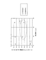
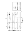
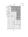
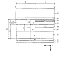
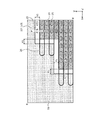
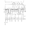
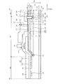
従来の炭化珪素半導体装置(炭化珪素を半導体材料として用いた半導体装置)の構造について、MOSFETを例に説明する。図21は、従来の炭化珪素半導体装置を半導体基板のおもて面側から見たレイアウトを示す平面図である。図22は、図21の切断線AA−AA’における断面構造を示す断面図である。図22には、活性領域101とエッジ終端領域102との間の領域(以下、境界領域とする)103の断面構造を示す。図23は、図21の一部を拡大して示す平面図である。図24,25は、それぞれ、図23の切断線CC−CC’および切断線DD−DD’における断面構造を示す断面図である。
A structure of a conventional silicon carbide semiconductor device (a semiconductor device using silicon carbide as a semiconductor material) will be described using a MOSFET as an example. FIG. 21 is a plan view showing a layout of a conventional silicon carbide semiconductor device viewed from the front side of a semiconductor substrate. FIG. 22 is a cross-sectional view showing a cross-sectional structure taken along section line AA-AA 'in FIG. FIG. 22 shows a cross-sectional structure of a region (hereinafter, referred to as a boundary region) 103 between the
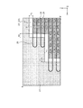
図23には、頂点BB,BB’を対頂点とする矩形枠で囲んだ、半導体基板(半導体チップ)110のコーナー部付近における活性領域101と境界領域103との境界付近の状態を示す。この矩形枠の頂点BBは半導体基板110のコーナー部側であり、頂点BB’は半導体基板110の中央部側である。半導体基板110のコーナー部とは、略矩形状の平面形状を有する半導体基板110の頂点である。図23には、n+型ソース領域124、p+型コンタクト領域125、トレンチ126およびp+型高濃度領域151のレイアウトを示し、ゲート絶縁膜127およびゲート電極128を図示省略する。
FIG. 23 shows a state near the boundary between the
図21〜25に示す従来の炭化珪素半導体装置は、活性領域101とエッジ終端領域102との間に、p+型高濃度領域151を有する境界領域103を備えたMOSFETである。活性領域101は、炭化珪素からなる半導体基板110の中央部に配置されている。活性領域101には、トレンチゲート構造の縦型MOSFETの複数の単位セルが配置され、このMOSFETの導通時に主電流が流れる。トレンチゲート構造(トレンチ126の内部にゲート絶縁膜127を介して埋め込まれたゲート電極128)は、半導体基板110のおもて面に平行な方向Xに延在するストライプ状に配置されている。
The conventional silicon carbide semiconductor device shown in FIGS. 21 to 25 is a MOSFET including a
エッジ終端領域102は、境界領域103と半導体基板110の端部との間の領域であり、境界領域103を介して活性領域101の周囲を囲む。エッジ終端領域102は、活性領域101の端部での電界集中を緩和して所定の耐圧(耐電圧)を保持する機能を有する。耐圧とは、pn接合部でアバランシェ降伏を起こし、ソース−ドレイン間の電流を増加してもそれ以上ソース−ドレイン間の電圧が増加しない限界の電圧である。エッジ終端領域102には、例えば、外側(半導体基板110の端部側)に配置されるほど不純物濃度を低くした複数のp-型領域141およびp--型領域142からなる接合終端(JTE:Junction Termination Extension)構造140等の耐圧構造が配置される。
The
境界領域103は、活性領域101とエッジ終端領域102との間において半導体基板110のおもて面全面に設けられたp+型高濃度領域151で構成される。p+型高濃度領域151は、MOSFETのp型ベース領域123の、境界領域103に延在する部分(以下、p型ベース領域延在部とする)123’に設けられ、n+型ソース領域124およびp+型コンタクト領域125に接する。また、p+型高濃度領域151は、JTE構造140の最も内側(半導体基板110の中央部側)のp-型領域141に接する。p+型高濃度領域151は、p型ベース領域123よりも不純物濃度が高い。
The
p+型高濃度領域151は、p型ベース領域123を低抵抗化する機能を有する。p型ベース領域123を低抵抗化することで、オフ時のアバランシェ降伏161により高電界がかかる活性領域101の端部またはエッジ終端領域102で主に発生する正孔電流162がソース電極131へ引き抜かれる際にp型ベース領域123の電位の持ち上がりが防止される。例えば、p型ベース領域123の電位の持ち上がりが過剰になると、正孔電流162が引き抜かれるコンタクト付近で、厚さの薄いゲート絶縁膜127にかかる電界が大きくなるため、ゲート絶縁膜127の寿命短縮や絶縁破壊につながる。
The p + -type high-
また、p+型高濃度領域151は、MOSFETのp型ベース領域123のシート抵抗を小さくするために、MOSFETのn+型ソース領域124に隣接して配置されている。このp+型高濃度領域151は、通常、アルミニウム(Al)等のp型不純物のイオン注入と、当該イオン注入後に行う不純物活性化のための熱処理(以下、活性化アニールとする)と、により形成される。p+型高濃度領域151を形成するためのイオン注入条件は、例えば、最大加速エネルギーを350keVとし、p型不純物の総ドーズ量を5.15×10¹⁵/cm2とする。
The p + -type high-
符号121,111,112は、半導体基板110を構成する炭化珪素エピタキシャル層である。符号122,122’,129,132,133,143,144は、それぞれ、n-型ドリフト領域、n型JFET領域、層間絶縁膜、ゲートパッド、ドレイン電極、n型チャネルストッパー領域およびフィールド酸化膜である。符号130は、半導体部とオーミック接触する金属膜である。符号152,153は、それぞれ、ゲート電位の導電層およびゲートランナーである。符号137,138は、p+型領域である。符号Yは、トレンチ126が並ぶ方向である。符号Zは、半導体基板110の深さ方向である。
このような従来の炭化珪素半導体装置として、1つのトレンチの内部のゲート電極で1つのMOSゲートを構成した単位セルを複数備えたトレンチゲート型MOSFETであって、最も外側のp+型コンタクト領域をエッジ終端領域まで延在させて、JTE構造の最も内側のp型領域と接触させた装置が提案されている(例えば、下記特許文献1(第0044段落)参照。)。下記特許文献1では、メサ領域内のn+型ソース領域が、同じメサ領域内のp+型コンタクト領域、または、トレンチの終端部付近のp+型コンタクト領域に接していることで、すべてのn+型ソース領域を同電位に固定している。
Such a conventional silicon carbide semiconductor device is a trench gate type MOSFET including a plurality of unit cells each of which forms one MOS gate with a gate electrode inside one trench, and has an outermost p + -type contact region. A device has been proposed which extends to the edge termination region and is in contact with the innermost p-type region of the JTE structure (for example, see Patent Document 1 (paragraph 0044) below). In
しかしながら、上述した従来の炭化珪素半導体装置(図21〜25参照)では、半導体基板110が高温度(例えば125℃以上程度)となる条件で、オフ状態を維持する際に、ゲート電極128にソース電極131の電位に対して負バイアスとなるゲート電圧Vg(ゲート電圧Vg<0:以下、ゲート負バイアスとする)が長時間印加されたとする。この場合、ゲートしきい値電圧Vthが初期状態と比べてマイナス方向(低くなる方向)へ大きく変動し、初期状態と比べて低いゲート電圧Vgで通電してドレイン電流Idが流れ始める。このため、ドレイン電流Idのゲインカーブ(図26参照)が初期状態と比べてゲート電圧Vgのマイナス方向へ大きく変位する。
However, in the above-described conventional silicon carbide semiconductor device (see FIGS. 21 to 25), when the
初期状態とは、ゲート電極128へのゲート負バイアスの印加時間の合計が0(ゼロ)Vの状態である。ドレイン電流Idとは、通電時にn+型ドレイン領域(n+型出発基板121)からn+型ソース領域124へ向かって移動する電子の流れである。ドレイン電流Idのゲインカーブとは、ゲート電極128にソース電極131の電位に対して正バイアスとなるゲート電圧Vg(ゲート電圧Vg≧0:以下、ゲート正バイアスとする)を印加して当該ゲート電圧Vgを増加させていったときに、ゲートしきい値電圧Vth以上のゲート電圧Vgで流れ始め、さらにゲート電圧Vgの増加に伴って増加するドレイン電流Idの増加曲線である。
The initial state is a state in which the total application time of the gate negative bias to the
ドレイン電流Idの所定の電流量に対応するゲート電圧Vgの初期状態時からの変動に規則性はなく、その変動量ΔVgはゲート電極128に印加されたゲート負バイアスの任意の印加時間でマイナス方向へ最大となる。かつ、このゲート電圧Vgの変動量ΔVgは、初期状態時のゲート電圧Vgの変動量ΔVgと比べてプラス方向へ変動しない。したがって、ゲート電極128に印加されたゲート負バイアスの印加時間を時間軸とした場合、ゲート電圧Vgの変動量ΔVgは、最小の変動量ΔVgとなる初期状態時の最大値と、最大の変動量ΔVgとなる任意の印加時間時の最小値と、の間で規則性なく変動する。
The fluctuation of the gate voltage Vg corresponding to the predetermined amount of the drain current Id from the initial state is not regular, and the fluctuation amount ΔVg changes in the negative direction at an arbitrary application time of the gate negative bias applied to the
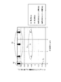
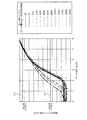
この現象は、ゲインカーブ内のドレイン電流Idの立ち上がり領域に顕著にあらわれる。この現象を検証した結果を図26,27に示す。図26は、従来の炭化珪素半導体装置のドレイン電流Idのゲインカーブの電流立ち上がり初期の領域を示す特性図である。図26の横軸は、通電時にゲート電極128に印加されるゲート電圧Vg(ゲート正バイアス)[V]である。図26の縦軸は、ドレイン電流Idを定格電流I0で割った規格化ドレイン電流である。一般にゲートしきい値電圧Vthは規格化ドレイン電流(=Id/I0)が10-3となるときのゲート電圧Vgとして定義される。
This phenomenon appears remarkably in the rising region of the drain current Id in the gain curve. The results of verifying this phenomenon are shown in FIGS. FIG. 26 is a characteristic diagram showing a region of a gain curve of a drain current Id of the conventional silicon carbide semiconductor device at an initial stage of current rise. The horizontal axis in FIG. 26 is the gate voltage Vg (gate positive bias) [V] applied to the
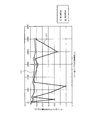
図26の注釈は、ゲート電極128に印加したゲート負バイアスの印加時間である。ゲート電極128へのゲート負バイアス印加時、ドレイン電極133とソース電極131との間の電圧(ソース−ドレイン電圧)は0(ゼロ)Vである。また、図26の注釈に示す「0h」の試料は上述した初期状態に相当する。図27は、図26のゲート電圧Vg(ゲート正バイアス)の初期状態時からの変動量ΔVgとオフ時のゲート電圧Vg(ゲート負バイアス)の印加時間との関係を示す特性図である。図27の横軸はゲート負バイアスの印加時間[時間(h:hour)]であり、縦軸はゲート正バイアスの初期状態時からの変動量ΔVgである。
The annotation in FIG. 26 is the application time of the gate negative bias applied to the
まず、従来の炭化珪素半導体装置(図21〜25参照)の構造を備えたMOSFETであって、半導体基板110が200℃の高温度となる条件でゲート電極128にゲート負バイアスを印加した複数の試料を用意した。これらの試料は、ゲート電極128に印加したゲート負バイアスが−5Vであり(ゲート電圧Vg=−5V)、当該ゲート負バイアスの印加時間が0h〜2500hの範囲内で異なっている。これらの試料に対して、室温(例えば25℃程度)でゲート電極128にゲート正バイアスを印加して通電した後に当該ゲート正バイアスを増加させてドレイン電流Idの電流量[A]を測定した結果を図26に示す。
First, a MOSFET having a structure of a conventional silicon carbide semiconductor device (see FIGS. 21 to 25), in which a plurality of
また、規格化ドレイン電流Id/I0の所定の電流量Id1/I0,Id2/I0(図26に符号171,172を付した破線で示す箇所)に対応するゲート正バイアスの初期状態時からの変動量ΔVgを図27に示す。図27には、例えば、ドレイン電流Idの電流量が定格電流I0の千分の一の電流量Id1/I0(=10-3)となる測定点(以下、第1測定点171’)、および、ドレイン電流Idの電流量が第1測定点171’のドレイン電流Idの電流量Id1の百万分の一の電流量Id2/I0(=10-9)となる測定点(以下、第2測定点172’)、におけるゲート正バイアスの初期状態時からの変動量ΔVgと、を示す。
In addition, fluctuations from the initial state of the gate positive bias corresponding to the predetermined current amounts Id1 / I0 and Id2 / I0 of the normalized drain current Id / I0 (points indicated by broken lines denoted by
図27に示すように、第1測定点171’でのドレイン電流Idの電流量に対応するゲート正バイアスは、ゲート電極128に印加したゲート負バイアスの印加時間が異なるすべての試料で5.2Vとなった。すなわち、第1測定点171’でのドレイン電流Idの電流量に対応するゲート正バイアスの初期状態時からの変動量ΔVgは、ゲート負バイアス印加の有無によらず、ほぼ0(ゼロ)Vであった。それに対して、第1測定点171’と比べてゲート電極128に印加されたゲート正バイアスがゲートしきい値電圧Vthに近いゲート電圧Vgを印加した状態にある第2測定点172’でのドレイン電流Idの電流量に対応するゲート正バイアスの初期状態時からの変動量ΔVgは最大で−1.2Vであった。
As shown in FIG. 27, the gate positive bias corresponding to the amount of the drain current Id at the
この図27に示す結果から、ドレイン電流Idの立ち上がり領域(具体的には、第2測定点172’付近)で、高温度およびゲート負バイアス印加の悪影響によりゲートしきい値電圧Vthの特性が不安定になる、いわゆるNBTI(Negative Bias Temperature Instability)となることがわかる。このように、ドレイン電流Idのゲインカーブは、ドレイン電流Idの立ち上がり領域にのみ、初期状態と比べてゲート電圧Vgのマイナス方向へ大きく変位する。
From the results shown in FIG. 27, it can be seen that in the rising region of the drain current Id (specifically, in the vicinity of the
このようなドレイン電流Idのゲインカーブの変位は、ゲート電極128に0V以下のゲート電圧Vgを印加してオフ状態を維持する際に、逆方向リーク電流の増加、または、過大なリーク電流による熱暴徒および素子破壊を引き起こす問題がある。
Such a displacement of the gain curve of the drain current Id is caused by an increase in reverse leakage current or an increase in heat due to excessive leakage current when a gate voltage Vg of 0 V or less is applied to the
この発明は、上述した従来技術による問題点を解消するため、高温度(200℃以上程度)においてゲート電圧制御による電流制御性を向上させることができる炭化珪素半導体装置を提供することを目的とする。 An object of the present invention is to provide a silicon carbide semiconductor device capable of improving current controllability by gate voltage control at a high temperature (about 200 ° C. or higher) in order to solve the above-described problems caused by the conventional technology. .
上述した課題を解決し、本発明の目的を達成するため、この発明にかかる半導体装置は、次の特徴を有する。第1主面および第2主面を有する第1導電型の半導体基板に、主電流が流れる活性領域が設けられている。終端領域は、前記活性領域の周囲を囲む。第2導電型エピタキシャル層は、前記半導体基板の一部をなし、前記半導体基板の前記第1主面を形成する。前記活性領域において、前記第2導電型エピタキシャル層の前記第1主面側の表面層に、第1導電型の第1半導体領域が選択的に設けられている。前記活性領域と前記終端領域との境界領域において、前記第2導電型エピタキシャル層の前記第1主面側の表面層に、第2導電型の第2半導体領域が選択的に設けられている。前記第2半導体領域は、前記第2導電型エピタキシャル層よりも不純物濃度が高い。第2導電型の第3半導体領域は、前記第2導電型エピタキシャル層の、前記第1半導体領域および前記第2半導体領域を除いた部分である。第1導電型の第4半導体領域は、前記半導体基板の、前記第2導電型エピタキシャル層を除いた部分である。トレンチは、前記第1半導体領域および前記第3半導体領域を貫通して前記第4半導体領域に達する。ゲート電極は、前記トレンチの内部にゲート絶縁膜を介して設けられている。第1電極は、前記第1半導体領域および前記第3半導体領域に電気的に接続されている。第2電極は、前記半導体基板の前記第2主面に設けられている。前記第2半導体領域は、前記第1半導体領域と離して配置されている。前記第2半導体領域と前記第1半導体領域との間において前記半導体基板の前記第1主面に、前記第2導電型エピタキシャル層の前記第3半導体領域の部分が露出されている。 In order to solve the above-described problems and achieve the object of the present invention, a semiconductor device according to the present invention has the following features. An active region through which a main current flows is provided on a semiconductor substrate of a first conductivity type having a first main surface and a second main surface. A termination region surrounds the periphery of the active region. The second conductivity type epitaxial layer forms a part of the semiconductor substrate and forms the first main surface of the semiconductor substrate. In the active region, a first semiconductor region of a first conductivity type is selectively provided in a surface layer on the first main surface side of the second conductivity type epitaxial layer. In a boundary region between the active region and the termination region, a second semiconductor region of the second conductivity type is selectively provided on a surface layer on the first main surface side of the second conductivity type epitaxial layer. The second semiconductor region has a higher impurity concentration than the second conductivity type epitaxial layer. The third semiconductor region of the second conductivity type is a portion of the second conductivity type epitaxial layer excluding the first semiconductor region and the second semiconductor region. The fourth semiconductor region of the first conductivity type is a portion of the semiconductor substrate excluding the second conductivity type epitaxial layer. The trench penetrates the first semiconductor region and the third semiconductor region to reach the fourth semiconductor region. The gate electrode is provided inside the trench via a gate insulating film. The first electrode is electrically connected to the first semiconductor region and the third semiconductor region. The second electrode is provided on the second main surface of the semiconductor substrate. The second semiconductor region is disposed apart from the first semiconductor region. A portion of the third semiconductor region of the second conductivity type epitaxial layer is exposed on the first main surface of the semiconductor substrate between the second semiconductor region and the first semiconductor region.
また、この発明にかかる半導体装置は、上述した発明において、前記トレンチは、前記半導体基板の前記第1主面に平行な第1方向に直線状に延在する。前記第2半導体領域は、前記トレンチの端部付近において前記第1方向に前記第1半導体領域と離して配置されていることを特徴とする。 In the semiconductor device according to the present invention, in the above-described invention, the trench extends linearly in a first direction parallel to the first main surface of the semiconductor substrate. The second semiconductor region is arranged near the end of the trench in the first direction and separated from the first semiconductor region.
また、この発明にかかる半導体装置は、上述した発明において、前記トレンチは、前記第1方向に前記活性領域から前記境界領域にまで延在するストライプ状に複数配置されている。前記第1半導体領域は、隣り合う前記トレンチの間に配置されている。前記第2半導体領域は、複数の前記トレンチのうち、前記半導体基板の前記第1主面に平行で、かつ前記第1方向と直交する第2方向に最も前記境界領域寄りの最外トレンチと離して配置されている。前記第2半導体領域と前記最外トレンチとの間において前記半導体基板の前記第1主面に、前記第2導電型エピタキシャル層の前記第3半導体領域の部分が露出されていることを特徴とする。 Further, in the semiconductor device according to the present invention, in the above-described invention, a plurality of the trenches are arranged in a stripe shape extending from the active region to the boundary region in the first direction. The first semiconductor region is disposed between the adjacent trenches. The second semiconductor region is separated from an outermost trench closest to the boundary region in a second direction parallel to the first main surface of the semiconductor substrate and in a second direction orthogonal to the first direction, among the plurality of trenches. Is arranged. A portion of the third semiconductor region of the second conductivity type epitaxial layer is exposed on the first main surface of the semiconductor substrate between the second semiconductor region and the outermost trench. .
また、この発明にかかる半導体装置は、上述した発明において、前記第3半導体領域の、前記半導体基板の前記第1主面に露出する部分は、前記境界領域に配置され、前記活性領域の周囲を囲むことを特徴とする。 Further, in the semiconductor device according to the present invention, in the above-described invention, a portion of the third semiconductor region exposed on the first main surface of the semiconductor substrate is disposed in the boundary region, and a periphery of the active region is formed. It is characterized by being surrounded.
また、この発明にかかる半導体装置は、上述した発明において、前記第1方向において前記第2半導体領域から前記第1半導体領域までの第1距離は0.6μm以上であることを特徴とする。 In the semiconductor device according to the present invention, in the above-described invention, a first distance from the second semiconductor region to the first semiconductor region in the first direction is 0.6 μm or more.
また、この発明にかかる半導体装置は、上述した発明において、前記第2方向において前記第2半導体領域から前記最外トレンチまでの第2距離は0.6μm以上であることを特徴とする。 In the semiconductor device according to the present invention, in the above-described invention, a second distance from the second semiconductor region to the outermost trench in the second direction is 0.6 μm or more.
また、この発明にかかる半導体装置は、上述した発明において、前記第1方向において前記第2半導体領域から前記第1半導体領域までの第1距離は9.35μm以上であることを特徴とする。 In the semiconductor device according to the present invention, in the above-described invention, a first distance from the second semiconductor region to the first semiconductor region in the first direction is 9.35 μm or more.
また、この発明にかかる半導体装置は、上述した発明において、前記トレンチは、前記半導体基板の前記第1主面に平行な第1方向に前記活性領域から前記境界領域にまで延在するストライプ状に複数配置されている。前記第1半導体領域は、隣り合う前記トレンチの間に配置されている。前記第2半導体領域は、複数の前記トレンチのうち、前記半導体基板の前記第1主面に平行で、かつ前記第1方向と直交する第2方向に最も前記境界領域寄りの最外トレンチと離して配置されている。前記第2半導体領域と前記最外トレンチとの間において前記半導体基板の前記第1主面に、前記第2導電型エピタキシャル層の前記第3半導体領域の部分が露出されていることを特徴とする。 Further, in the semiconductor device according to the present invention, in the above-described invention, the trench is formed in a stripe shape extending from the active region to the boundary region in a first direction parallel to the first main surface of the semiconductor substrate. A plurality is arranged. The first semiconductor region is disposed between the adjacent trenches. The second semiconductor region is separated from an outermost trench closest to the boundary region in a second direction parallel to the first main surface of the semiconductor substrate and in a second direction orthogonal to the first direction, among the plurality of trenches. Is arranged. A portion of the third semiconductor region of the second conductivity type epitaxial layer is exposed on the first main surface of the semiconductor substrate between the second semiconductor region and the outermost trench. .
また、この発明にかかる半導体装置は、上述した発明において、前記第2方向において前記第2半導体領域から前記最外トレンチまでの第2距離は0.6μm以上であることを特徴とする。 In the semiconductor device according to the present invention, in the above-described invention, a second distance from the second semiconductor region to the outermost trench in the second direction is 0.6 μm or more.
また、この発明にかかる半導体装置は、上述した発明において、前記第2半導体領域の不純物濃度は、6.4×10¹⁴/cm2以下であることを特徴とする。 In the semiconductor device according to the present invention, in the above-described invention, the impurity concentration of the second semiconductor region is 6.4 × 10 14 / cm 2 or less.
また、この発明にかかる半導体装置は、上述した発明において、前記トレンチは、前記活性領域から前記境界領域にまで延在し、前記第2半導体領域よりも前記活性領域寄りの位置で終端していることを特徴とする。 In the semiconductor device according to the present invention, in the above-described invention, the trench extends from the active region to the boundary region, and terminates at a position closer to the active region than the second semiconductor region. It is characterized by the following.
また、この発明にかかる半導体装置は、上述した発明において、前記第3半導体領域の、前記半導体基板の前記第1主面に露出する部分に選択的に設けられた第2導電型の第5半導体領域をさらに備える。前記第5半導体領域は、前記第3半導体領域よりも不純物濃度が高い。前記第3半導体領域は、前記第5半導体領域を介して前記第1電極に電気的に接続されていることを特徴とする。 Further, in the semiconductor device according to the present invention, in the above-mentioned invention, the fifth semiconductor of the second conductivity type selectively provided in a portion of the third semiconductor region exposed to the first main surface of the semiconductor substrate. Further comprising an area. The fifth semiconductor region has a higher impurity concentration than the third semiconductor region. The third semiconductor region is electrically connected to the first electrode via the fifth semiconductor region.
また、この発明にかかる半導体装置は、上述した発明において、前記第5半導体領域は、前記第2導電型エピタキシャル層に第2導電型不純物がイオン注入されてなる拡散領域であることを特徴とする。 Further, in the semiconductor device according to the present invention, in the above-described invention, the fifth semiconductor region is a diffusion region formed by ion-implanting a second conductivity type impurity into the second conductivity type epitaxial layer. .
また、この発明にかかる半導体装置は、上述した発明において、前記第2半導体領域は、前記第2導電型エピタキシャル層に第2導電型不純物がイオン注入されてなる拡散領域であることを特徴とする。 Further, in the semiconductor device according to the present invention, in the above-mentioned invention, the second semiconductor region is a diffusion region formed by ion-implanting a second conductivity type impurity into the second conductivity type epitaxial layer. .
上述した発明によれば、高温度条件でゲート電極にゲート負バイアスが印加されたときに、第3半導体領域の、ゲート絶縁膜との界面に正孔が蓄積されることを抑制することができる。これにより、ゲート電極にゲートしきい値電圧以上のゲート正バイアスが印加されたときに第4半導体領域から第1半導体領域へ向かって流れる電流のゲインカーブが初期状態と比べてゲート電圧のマイナス方向へ変位することを抑制することができる。 According to the invention described above, it is possible to suppress the accumulation of holes at the interface between the third semiconductor region and the gate insulating film when a gate negative bias is applied to the gate electrode under a high temperature condition. . As a result, when a gate positive bias equal to or higher than the gate threshold voltage is applied to the gate electrode, the gain curve of the current flowing from the fourth semiconductor region toward the first semiconductor region becomes smaller in the negative direction of the gate voltage than in the initial state. Displacement can be suppressed.
本発明にかかる炭化珪素半導体装置によれば、高温度(200℃以上程度)においてゲート電圧制御による電流制御性を向上させることができるという効果を奏する。 ADVANTAGE OF THE INVENTION According to the silicon carbide semiconductor device concerning this invention, there exists an effect that the current controllability by gate voltage control can be improved at high temperature (about 200 degreeC or more).
以下に添付図面を参照して、この発明にかかる炭化珪素半導体装置の好適な実施の形態を詳細に説明する。本明細書および添付図面においては、nまたはpを冠記した層や領域では、それぞれ電子または正孔が多数キャリアであることを意味する。また、nやpに付す+および−は、それぞれそれが付されていない層や領域よりも高不純物濃度および低不純物濃度であることを意味する。なお、以下の実施の形態の説明および添付図面において、同様の構成には同一の符号を付し、重複する説明を省略する。 Hereinafter, preferred embodiments of a silicon carbide semiconductor device according to the present invention will be described in detail with reference to the accompanying drawings. In the present specification and the accompanying drawings, in a layer or a region entitled with n or p, it means that electrons or holes are majority carriers, respectively. Further, + and-attached to n and p mean that the impurity concentration is higher and lower than that of the layer or region to which n or p is not added. In the following description of the embodiments and the accompanying drawings, the same components are denoted by the same reference numerals, and overlapping description will be omitted.
(実施の形態1)
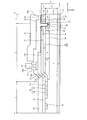
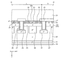
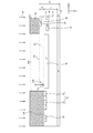
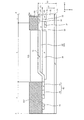
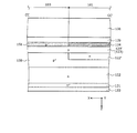
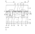
実施の形態1にかかる炭化珪素半導体装置(炭化珪素(SiC)を半導体材料として用いた半導体装置)の構造について、MOSFETを例に説明する。図1は、実施の形態1にかかる炭化珪素半導体装置を半導体基板のおもて面側から見たレイアウトを示す平面図である。図2は、図1の切断線A−A’における断面構造を示す断面図である。図2には、活性領域1とエッジ終端領域2との間の領域(境界領域)3の断面構造を示す。図3は、図1の一部を拡大して示す平面図である。図4,5は、それぞれ、図3の切断線C−C’および切断線D−D’における断面構造を示す断面図である。
(Embodiment 1)
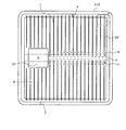
A structure of a silicon carbide semiconductor device (a semiconductor device using silicon carbide (SiC) as a semiconductor material) according to the first embodiment will be described using a MOSFET as an example. FIG. 1 is a plan view showing a layout of the silicon carbide semiconductor device according to the first embodiment as viewed from the front side of a semiconductor substrate. FIG. 2 is a cross-sectional view showing a cross-sectional structure taken along a cutting line AA ′ in FIG. FIG. 2 shows a sectional structure of a region (boundary region) 3 between the
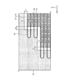
図3には、図1の頂点B,B’を対頂点とする矩形枠で囲んだ、半導体基板(半導体チップ)10のコーナー部付近における活性領域1と境界領域3との境界付近の状態を示す。この矩形枠の頂点B付近は半導体基板10のコーナー部側の部分であり、頂点B’付近は半導体基板10の中央部側の部分である。半導体基板10のコーナー部とは、略矩形状の平面形状を有する半導体基板10の頂点である。図3には、n+型ソース領域(第1半導体領域)24、p+型コンタクト領域25、トレンチ26およびp+型高濃度領域(第2半導体領域)51のレイアウトを示し、ゲート絶縁膜27およびゲート電極28を図示省略する。
FIG. 3 shows a state near the boundary between the
図1〜5に示す実施の形態1にかかる炭化珪素半導体装置は、活性領域1とエッジ終端領域2との間に、p+型高濃度領域51を有する境界領域3を備えたトレンチゲート構造の縦型MOSFETである。活性領域1は、炭化珪素からなる半導体基板10の中央部に配置されている。活性領域1には、トレンチゲート構造の縦型MOSFETの複数の単位セル(素子の構成単位)が配置され、このMOSFETの導通(通電)時に主電流(ドレイン電流Id)が流れる。トレンチゲート構造は、半導体基板10のおもて面13aから所定深さに達するトレンチ26の内部にゲート絶縁膜27を介して埋め込まれたゲート電極28で構成されたMOSゲートを有する。
The silicon carbide semiconductor device according to the first embodiment shown in FIGS. 1 to 5 has a trench gate structure including
活性領域1は、後述するn+型ソース領域24の外周よりも内側(半導体基板10の中央側)の領域であり、例えば略矩形状の平面形状を有する。後述する第1方向Xにおいてn+型ソース領域24の外周とは、隣り合うトレンチ26間において当該トレンチ26に沿って第1方向Xに直線状に延びるn+型ソース領域24の第1方向Xの端部である。後述する第2方向Yにおいてn+型ソース領域24の外周とは、第2方向Yに最も外側(半導体基板10の端部側)のトレンチ(最外トレンチ)26の内側の側壁とn+型ソース領域24との境界である。エッジ終端領域2は、p+型高濃度領域51と後述するJTE構造40のp-型領域41との境界よりも外側の領域である。
The
半導体基板10は、n+型ドレイン領域となる炭化珪素からなるn+型出発基板21のおもて面13a上にn-型ドリフト領域(第4半導体領域)22およびp型ベース領域(第3半導体領域)23となる各炭化珪素エピタキシャル層11,12を順にエピタキシャル成長させてなるエピタキシャル基板である。この半導体基板10において、p型炭化珪素エピタキシャル層(第2導電型エピタキシャル層)12が露出する主面(第1主面)をおもて面13aとし、n+型出発基板21の裏面が露出する主面(第2主面)を裏面とする。活性領域1において、n-型炭化珪素エピタキシャル層11の内部には、後述する第1,2p+型領域37,38がそれぞれ選択的に設けられている。n-型炭化珪素エピタキシャル層11の、第1,2p+型領域37,38を除いた部分がn-型ドリフト領域22である。
The
また、活性領域1において、p型炭化珪素エピタキシャル層12の表面領域(半導体基板10のおもて面13aの表面層)には、n+型ソース領域24およびp+型コンタクト領域25がそれぞれ選択的に設けられている。n+型ソース領域24は、p型炭化珪素エピタキシャル層12への例えばリン(P)等のn型不純物のイオン注入により形成される。p+型コンタクト領域25およびp+型高濃度領域51は、p型炭化珪素エピタキシャル層12への例えばアルミニウム(Al)等のp型不純物のイオン注入により形成される。p型炭化珪素エピタキシャル層12の、n+型ソース領域24、p+型コンタクト領域25およびp+型高濃度領域51を除いた部分がp型ベース領域23である。
In
p型ベース領域23は、活性領域1よりも外側へ延在し、境界領域3とエッジ終端領域2との境界付近に位置する後述する段差13のステア13bで終端している。以下、p型ベース領域23の、活性領域1よりも外側の部分をp型ベース領域延在部23’とする。具体的には、p型ベース領域延在部23’は、後述する第1方向Xにおいて、p型ベース領域23の、n+型ソース領域24の外周よりも外側の部分である。p型ベース領域延在部23’は、後述する第2方向Yにおいて、p型ベース領域23の、最も外側のトレンチ26よりも外側の部分である。p型ベース領域延在部23’は、略矩形状に活性領域1の周囲を囲む。
The p-
トレンチ26は、半導体基板10のおもて面13aからn+型ソース領域24およびp型ベース領域23を深さ方向Zに貫通してn-型ドリフト領域22に達する。トレンチ26は、両端部がそれぞれ半導体基板10の対辺付近に位置するように、半導体基板10のおもて面13aに平行な方向(以下、第1方向とする)Xに延在するストライプ状に配置されている。トレンチ26の端部は、活性領域1から外側へ延在し、境界領域3で終端している。トレンチ26の端部は、p+型高濃度領域51にまで達していてもよい(図3参照)。トレンチ26は、両端部ともにそれぞれ隣り合う他のトレンチ26と端部同士を連結した略環状の平面形状を有していてもよい。
トレンチ26の内部には、ゲート絶縁膜27を介してゲート電極28が設けられている。1つのトレンチ26の内部に配置されたゲート電極28と、当該トレンチ26によって分離された隣り合うメサ領域と、でMOSFETの1つの単位セルが構成される。メサ領域に設けられた領域は、ゲート絶縁膜27によってゲート電極28と電気的に絶縁されている。メサ領域とは、隣り合うトレンチ26間の領域である。MOSFETの単位セルは、第1方向Xに延在するストライプ状に複数配置されている。すなわち、p型ベース領域23、n+型ソース領域24、トレンチ26、ゲート絶縁膜27およびゲート電極28は、第1方向Xに延在するストライプ状に配置されている。
A
n+型ソース領域24は、トレンチ26の側壁からメサ領域を挟んで当該トレンチ26に隣り合う他のトレンチ26の側壁にまで達するように、活性領域1におけるメサ領域の全面に設けられている。p+型コンタクト領域25は、第1方向Xに所定間隔で、n+型ソース領域24の内部に点在して配置されている。p+型コンタクト領域25は、後述する金属膜30とn+型ソース領域24およびp+型コンタクト領域25とのコンタクト抵抗を低減する機能を有する。このp+型コンタクト領域25により、金属膜30と半導体部とのコンタクト(電気的接触部)の電圧−電流特性がオーミック性(直線性)を示す。このため、ソース電極(第1電極)31と半導体部との電位差を小さくすることができる。
The n +
ソース電極31と半導体部との電位差が小さくなることによって、n+型ソース領域24、p型ベース領域23およびn-型ドリフト領域22からなるnpn寄生バイポーラ動作によるゲート絶縁膜27の絶縁破壊を防止することができる。半導体基板10のおもて面13aからトレンチ26の底面よりもn+型出発基板21側に深い位置において、n-型ドリフト領域22の内部には、第1,2p+型領域37,38がそれぞれ選択的に設けられている。第1p+型領域37は、トレンチ26の底面よりもn+型出発基板21側に深い位置に配置され、深さ方向Zにトレンチ26の底面に対向する。トレンチ26の底面が第1p+型領域37の内部で終端していてもよい。
Since the potential difference between the
第2p+型領域38は、メサ領域において、p型ベース領域23よりもn+型出発基板21側に深い位置に配置され、かつp型ベース領域23に接する。第2p+型領域38は、トレンチ26から離して設けられている。第1,2p+型領域37,38は、第1方向Xと直交し、かつ半導体基板10のおもて面13aに平行な方向(以下、第2方向とする)Yに交互に繰り返し配置されている。これら第1,2p+型領域37,38を設けることで、MOSFETのオフ時にゲート絶縁膜27にかかる電界の抑制と、耐圧向上と、を実現可能である。第1,2p+型領域37,38間のn型JFET領域22’の不純物濃度を、n-型ドリフト領域22の不純物濃度よりも高くしてもよい。
The second p + -
また、第1,2p+型領域37,38は、第1方向Xに外側へ後述する段差13のコーナー部13cまで延在し、当該段差13のコーナー部13cにおいてp+型高濃度領域51を覆う。また、第2p+型領域38は、第2方向Yにおいて最も外側のトレンチ26よりも外側にも配置されている。第2方向Yにおいて最も外側のトレンチ26よりも外側にも配置された第2p+型領域38は、p型ベース領域延在部23’ よりもn+型出発基板21側に深い位置に配置され、かつp型ベース領域延在部23’に接する。かつ、当該第2p+型領域38は、第2方向Yに外側へ段差13のコーナー部13cまで延在し、当該段差13のコーナー部13cにおいてp+型高濃度領域51を覆う。
The first and second p + -
層間絶縁膜29は、半導体基板10のおもて面13aの全面に設けられ、ゲート電極28を覆う。層間絶縁膜29を深さ方向Zに貫通する第1コンタクトホール29aが設けられている。第1コンタクトホール29aは、活性領域1におけるメサ領域(すなわちn+型ソース領域24およびp+型コンタクト領域25)を露出する。各メサ領域は、それぞれ異なる第1コンタクトホール29aに露出されている。第1コンタクトホール29aは、例えば第1方向Xに所定間隔で点在しており、それぞれ異なるp+型コンタクト領域25を露出する。各第1コンタクトホール29aの内部において半導体基板10のおもて面13a上に、それぞれ金属膜30が設けられている。
The
金属膜30は、n+型ソース領域24およびp+型コンタクト領域25に接し、電圧−電流特性がオーミック性を示すコンタクトを形成している。金属膜30は、例えばニッケルシリサイド(NiSi)膜である。ソース電極31は、金属膜30を介してn+型ソース領域24、p+型コンタクト領域25およびp型ベース領域23に電気的に接続されている。ソース電極31は、半導体基板10のおもて面13aにおいて活性領域1のほぼ全面を覆う。ソース電極31は、ソースパッドを兼ねる。ソース電極31は、層間絶縁膜29上に延在し、境界領域3で終端していてもよい。ソース電極31は、例えばアルミニウム−シリコン(Al−Si)膜であってもよい。
The
また、活性領域1において層間絶縁膜29上には、例えば活性領域1の、境界領域3との境界付近に、ソース電極31と離してゲートパッド32が設けられている。ゲートパッド32は、例えば、略矩形状の平面形状を有する。ゲートパッド32は、例えばソース電極31と同じ材料で形成される。ゲートパッド32には、後述する導電層52およびゲートランナー53を介してすべてのゲート電極28が電気的に接続されている。ドレイン電極(第2電極)33は、活性領域1からエッジ終端領域2にわたって、半導体基板10の裏面全体に設けられている。ドレイン電極33は、n+型ドレイン領域であるn+型出発基板21の裏面に接し、電圧−電流特性がオーミック性を示すコンタクトを形成する。
In the
エッジ終端領域2は、境界領域3と半導体基板10の端部との間の領域であり、境界領域3を介して略矩形状に活性領域1の周囲を囲む。エッジ終端領域2は、活性領域1の端部での電界集中を緩和して所定の耐圧(耐電圧)を保持する機能を有する。耐圧とは、リーク電流が過度に増大せず、素子が誤動作や破壊を起こさない限界の電圧である。エッジ終端領域2の全域にわたってp型炭化珪素エピタキシャル層12が除去されることで、半導体基板10のおもて面13aにエッジ終端領域2を活性領域1よりも低くした(n+型出発基板21側に凹ませた)段差13が形成されている。この段差13により、エッジ終端領域2に新たに半導体基板10のおもて面13a’が形成される。
The
エッジ終端領域2における半導体基板10のおもて面13a’には、n-型炭化珪素エピタキシャル層11が露出されている。段差13の形成時に、p型炭化珪素エピタキシャル層12とともにn-型炭化珪素エピタキシャル層11が所定深さで除去されてもよい。段差13のステア13bは、例えば境界領域3に位置している。段差13のステア13bとは、半導体基板10のおもて面のうち、半導体基板10の内側部分のおもて面13a(上段の面)と、半導体基板10の外側部分のおもて面13a’(下段の面)と、を連結する面である。段差13のステア13bには、後述するp+型高濃度領域51が露出されている。段差13の下段の面である半導体基板10の外側部分のおもて面13a’は、境界領域3まで延在していてもよい。
On
エッジ終端領域2において半導体基板10のおもて面13a’の表面層には、例えば、外側に配置されるほど不純物濃度を低くした複数のp型領域(ここでは例えば2つのp型領域に内側から順に符号41,42を付す)からなる接合終端(JTE)構造40等の耐圧構造が配置される。JTE構造40の最も内側のp-型領域41は、境界領域3を介して活性領域1の周囲を囲む。JTE構造40のp--型領域42は、p-型領域41の外側に隣接して配置され、p-型領域41の周囲を囲む。エッジ終端領域2における半導体基板10のおもて面13a’からの深さは、p-型領域41およびp--型領域42よりも例えば第2p+型領域38で深くなっている。
In the surface layer of the
これらp-型領域41およびp--型領域42の内部に、オフ時に第2p+型領域38とn-型ドリフト領域22とpn接合面の端部から外側に向かって伸びる空乏層が広がることで、エッジ終端領域2での耐圧が確保される。また、エッジ終端領域2において半導体基板10のおもて面13a’の表面層には、JTE構造40よりも外側で、かつJTE構造40と離して、n型チャネルストッパー領域43が選択的に設けられている。n型チャネルストッパー領域43は、半導体基板10の端部(半導体基板10の側面)に露出されている。エッジ終端領域2において、半導体基板10のおもて面13a’は、半導体基板10と層間絶縁膜29との間に設けられたフィールド酸化膜44で覆われている。
The depletion layer extending outward from the ends of the second p + -
境界領域3は、活性領域1とエッジ終端領域2との間において半導体基板10のおもて面13aの表面層に設けられたp+型高濃度領域51で構成される。p+型高濃度領域51は、例えば、アルミニウム等のp型不純物のイオン注入によりp型ベース領域延在部23’の表面領域に形成されている。p+型高濃度領域51は、第1方向Xにおいて活性領域1のn+型ソース領域24と離して配置され、かつ第2方向Yにおいて最も外側のトレンチ26の外側の側壁と離して配置されている。第2方向Yにおいてp+型高濃度領域51と最も外側のトレンチ26との間に、n+型ソース領域24およびp+型コンタクト領域25は設けられていない。
The
第1方向Xにおいてp+型高濃度領域51とn+型ソース領域24とに挟まれた部分、および、第2方向Yにおいてp+型高濃度領域51と最も外側のトレンチ26とに挟まれた部分、はp型炭化珪素エピタキシャル層12で構成されたp型ベース領域延在部23’の一部であり、活性領域1と境界領域3との境界に沿って半導体基板10のおもて面13aに露出されている(図3のハッチングされていない部分(図9,11,13,15,17においても同様))。すなわち、略矩形状の平面形状を有する活性領域1の1対の対辺に沿って延在する略直線状に、または、略矩形状の平面形状を有する活性領域1の周囲を囲む略矩形状に、活性領域1と境界領域3との境界に沿って半導体基板10のおもて面13aにp型ベース領域延在部23’が露出されている。
A portion between the p + -type high-
図3には、半導体基板10のコーナー部の状態のみを示すが、活性領域1と境界領域3との境界の第2方向Yに平行な対辺に沿って、p+型高濃度領域51をn+型ソース領域24から離して配置した状態となっている。活性領域1と境界領域3との境界の第1方向Xに平行な対辺に沿って、p+型高濃度領域51を最も外側のトレンチ26から離して配置した状態となっている。これによって、p型ベース領域延在部23’の、第1方向Xにおいてp+型高濃度領域51とn+型ソース領域24とに挟まれた部分、または、第2方向Yにおいてp+型高濃度領域51と最も外側のトレンチ26とに挟まれた部分、もしくはその両方の部分を、結晶欠陥が存在しないp型炭化珪素エピタキシャル層12で構成することができる。
FIG. 3 shows only the state of the corner portion of the
第1方向Xにおいてp+型高濃度領域51からn+型ソース領域24までの第1距離X1は例えば0.6μm以上程度とするとよい。第2方向Yにおいてp+型高濃度領域51から最も外側のトレンチ26までの第2距離Y1は例えば0.6μm以上程度とするとよい。これら第1,2距離X1,Y1の条件は少なくとも一方の条件が満たされていれば、後述する本発明の効果が得られる。第1,2距離X1,Y1の条件をともに満たす場合、第1,2距離X1,Y1は等しい(X1=Y1)。半導体基板10のおもて面13a側から見て、活性領域1の周囲は0.6μm以上の幅を有するp型ベース領域延在部23’に囲まれ、当該p型ベース領域延在部23’の周囲はp+型高濃度領域51に囲まれる。
In the first direction X, the first distance X1 from the p + -type high-
このように活性領域1とp+型高濃度領域51との間に、p型炭化珪素エピタキシャル層12で構成されたp型ベース領域延在部23’が配置される。これによって、高温度(例えば125℃以上程度)となる条件で、ゲート電極28にソース電極31の電位に対して負バイアスとなるゲート電圧Vg(ゲート電圧Vg<0:ゲート負バイアス)が長時間印加されたとしても、ドレイン電流Idの所定の電流量に対応するゲート電圧Vgの初期状態時からの変動量ΔVgを低減することができる。これにより、高温度条件でのゲート負バイアス印加によって、ゲートしきい値電圧Vthの特性が不安定になる期間、すなわちNBTIとなる期間を少なくすることができる。また、高温度となる条件で、ゲート電極28にゲート負バイアスが長時間印加されたとしても、ドレイン遮断電流(リーク電流)Idssの電流量を初期状態時に近づけることができる。
Thus, between
ゲート電圧Vgの初期状態時からの変動量ΔVgとは、初期状態でのゲート電圧Vgから、ゲート負バイアスを印加した状態でのゲート電圧Vgを減算した値(差分)である。通電時とは、ゲート電極28にソース電極31の電位に対して正バイアスとなるゲート電圧Vg(ゲート電圧Vg≧0:ゲート正バイアス)を印加して当該ゲート電圧Vgを増加させていき、ゲート電圧Vgがゲートしきい値電圧Vth以上となったときである。ドレイン電流Idは、通電後に流れ始め、ゲート電圧Vgの増加に伴って増加する。初期状態とは、ゲート電極28にゲート負バイアスが印加されていない状態、すなわちゲート電極28へのゲート負バイアスの印加時間の合計が0(ゼロ)Vの状態である。
The variation ΔVg of the gate voltage Vg from the initial state is a value (difference) obtained by subtracting the gate voltage Vg in the state where a gate negative bias is applied from the gate voltage Vg in the initial state. The term “energized” means that a gate voltage Vg (gate voltage Vg ≧ 0: gate positive bias) which becomes a positive bias with respect to the potential of the
また、p+型高濃度領域51は、境界領域3における半導体基板10のおもて面13aに露出されている。かつ、p+型高濃度領域51は、段差13のステア13bおよびコーナー部13cから段差13の下段の面である半導体基板10の外側部分のおもて面に13a’にわたって露出されている。段差13のコーナー部13cとは、段差13の下段の面である半導体基板10の外側部分のおもて面13a’と段差13のステア13bとの境界である。p+型高濃度領域51は、段差13のコーナー部13cにおいて第1方向Xにn-型ドリフト領域22および第1,2p+型領域37,38に接し、第2方向Yに第2p+型領域38に接する。
The p + -type high-
p+型高濃度領域51は、第1,2方向X,YにJTE構造40の最も内側のp-型領域41に接する。p+型高濃度領域51は、第1,2p+型領域37,38よりも外側へ延在していてもよい。この場合、p+型高濃度領域51は、第1,2p+型領域37,38とJTE構造40のp-型領域41との間においてn-型ドリフト領域22に接する。p+型高濃度領域51の表面全体がゲート絶縁膜27、層間絶縁膜29およびフィールド酸化膜44からなる絶縁膜で覆われている。すなわち、p+型高濃度領域51は、金属膜30に直接接していない。p+型高濃度領域51は、p型ベース領域延在部23’(すなわちp型ベース領域23)を介してソース電極31に電気的に接続されている。
The p + -type high-
また、p+型高濃度領域51は、p型ベース領域23よりも不純物濃度が高い。p+型高濃度領域51は、p型ベース領域23を低抵抗化する機能を有する。p型ベース領域23を低抵抗化することで、オフ時のアバランシェ降伏により電界が集中するエッジ終端領域2と境界領域3との境界付近または活性領域1の端部で主に発生する正孔電流がソース電極31へ引き抜かれる際にp型ベース領域延在部23’(すなわちp型ベース領域23)の電位が持ち上がることを防止することができる。これによって、厚さの薄いゲート絶縁膜27にかかる電界を緩和することができ、ゲート絶縁膜27の寿命を延ばしたり、ゲート絶縁膜27の絶縁破壊を防止することができる。
The p + -type
境界領域3において、フィールド酸化膜44上には、ポリシリコン(poly−Si:)からなる導電層52と、例えばソース電極31と同じ材料で形成されたゲートランナー53と、が設けられている(図2参照)。導電層52には、図示省略する部分ですべてのゲート電極28が電気的に接続されている。導電層52は、層間絶縁膜29で覆われている。ゲートランナー53は、層間絶縁膜29を深さ方向に貫通する第2コンタクトホール29bを介して導電層52に接続されている。導電層52およびゲートランナー53は、略矩形状に活性領域1の周囲を囲む。ゲートランナー53は、ゲートパッド32(図1参照)に接続されている。
In the
特に限定しないが、例えば実施の形態1にかかるMOSFETが耐圧1200Vクラスである場合には、各部の寸法および不純物濃度は次の値をとる。n+型出発基板21の不純物濃度は、例えば1×10¹⁸/cm3程度である。n-型炭化珪素エピタキシャル層11の厚さt11は、例えば10μmである。n-型炭化珪素エピタキシャル層11(n-型ドリフト領域22)の不純物濃度は、例えば5×1015/cm3以上2×1016/cm3程度である。n型JFET領域22’の不純物濃度は、例えば1×1017/cm3程度である。
Although not particularly limited, for example, when the MOSFET according to the first embodiment has a withstand voltage of 1200 V class, the dimensions and impurity concentrations of the respective components take the following values. The impurity concentration of the n + -
第1p+型領域37の厚さt1は、例えば0.5μm程度であってもよい。第1p+型領域37は、例えば半導体基板10のおもて面13aから2μm程度の深さにまで達する。第2p+型領域38の厚さt2は、例えば1μm程度であってもよい。第2p+型領域38は、例えば半導体基板10のおもて面13aから2μm程度の深さにまで達する。第1,2p+型領域37,38の不純物濃度は、例えば1×10¹⁷/cm3以上1×1019/cm3以下程度であり、例えば1×1018/cm3程度であってもよい。
The thickness t1 of the first p + type region 37 may be, for example, about 0.5 μm. The first p + -
p型炭化珪素エピタキシャル層12の厚さt12は、例えば1μm程度である。p型炭化珪素エピタキシャル層12(p型ベース領域23)の不純物濃度は、例えば1×10¹⁶/cm3以上3×1018/cm3以下程度であり、例えば1×1017/cm3程度であってもよい。n+型ソース領域24の不純物濃度は、例えば1×1021/cm3程度である。p+型高濃度領域51の厚さt3は、例えば0.5μm程度である。p+型高濃度領域51の不純物濃度は、例えば5×1018/cm3以上1×1021/cm3以下程度である。
Thickness t12 of p-type silicon
次に、実施の形態1にかかる炭化珪素半導体装置の動作について説明する。ドレイン電極33にソース電極31に対して正の電圧(ソース−ドレイン電圧)が印加された状態で、ゲート電極28にゲートしきい値電圧Vth未満のゲート電圧Vgが印加される。これにより、p型ベース領域23とn-型ドリフト領域22との間のpn接合が逆バイアスされた状態となるため、活性領域1の逆方向耐圧が確保され、ドレイン電流Idは流れない。すなわち、MOSFETはオフ状態を維持する。このとき、例えば、ゲート電極28にゲート負バイアスを印加することで、MOSFETを確実にオフすることができる。
Next, the operation of the silicon carbide semiconductor device according to the first embodiment will be described. With a positive voltage (source-drain voltage) applied to the
一方、ソース−ドレイン電圧が印加された状態で、ゲート電極28にゲートしきい値電圧Vth以上のゲート電圧Vgが印加されると、p型ベース領域23の、n+型ソース領域24とn-型ドリフト領域22とに挟まれた、トレンチ26に沿った部分にn型の反転層(チャネル)が形成される。これによって、n+型出発基板21、n-型ドリフト領域22、p型ベース領域23の表面反転層およびn+型ソース領域24の経路で電流が流れ、MOSFETがオン状態となる。このように、ゲート電圧Vgを制御することによって、MOSFETのスイッチング動作を行うことができる。
On the other hand, the source - in a state in which the drain voltage is applied, the gate threshold voltage Vth or the gate voltage Vg is applied to the
実施の形態1にかかる炭化珪素半導体装置の製造方法について説明する。図6,7は、実施の形態1にかかる炭化珪素半導体装置の製造途中の状態を示す断面図である。まず、n+型出発基板21のおもて面に、n-型炭化珪素エピタキシャル層11をエピタキシャル成長させる。次に、フォトリソグラフィおよびイオン注入により、n-型炭化珪素エピタキシャル層11の内部に、第1,2p+型領域37,38を選択的に形成する。次に、エピタキシャル成長によりn-型炭化珪素エピタキシャル層11の厚さを増やして、n-型炭化珪素エピタキシャル層11を所定の厚さt11まで厚くする。
A method for manufacturing the silicon carbide semiconductor device according to the first embodiment will be described. FIGS. 6 and 7 are cross-sectional views showing the state of the silicon carbide semiconductor device according to the first embodiment in the process of being manufactured. First, n − -type silicon
次に、フォトリソグラフィおよびイオン注入により、n-型炭化珪素エピタキシャル層11の表面層に第2p+型領域38となるp+型領域を形成することで、第2p+型領域38を所定の厚さt2にまで厚くする。n-型炭化珪素エピタキシャル層11の、第1,2p+型領域37,38と、後の工程で形成されるp-型領域41、p--型領域42およびn型チャネルストッパー領域43と、を除いた部分がn-型ドリフト領域22となる。次に、n-型炭化珪素エピタキシャル層11の表面に、p型炭化珪素エピタキシャル層12をエピタキシャル成長させる。
Next, by forming ap + -type region serving as the second p + -
次に、エッジ終端領域2の全域にわたってp型炭化珪素エピタキシャル層12を除去して、半導体基板10のおもて面13aにエッジ終端領域2を活性領域1よりも低くした段差13を形成する。これにより、エッジ終端領域2における半導体基板10のおもて面13a’にn-型炭化珪素エピタキシャル層11が露出される。次に、異なる酸化膜マスクを用いてイオン注入を行うことにより、上述した所定領域にそれぞれn+型ソース領域24、p+型コンタクト領域25、p+型高濃度領域51、JTE構造40(p-型領域41、p--型領域42)およびn型チャネルストッパー領域43を選択的に形成する。
Next, the p-type silicon
n+型ソース領域24、p+型コンタクト領域25、p+型高濃度領域51、JTE構造40およびn型チャネルストッパー領域43の形成順序は種々変更可能である。また、p+型高濃度領域51は、p+型コンタクト領域25と同時に形成可能である。例えば、n+型ソース領域24、JTE構造40およびn型チャネルストッパー領域43の形成後に、p+型コンタクト領域25およびp+型高濃度領域51を形成する場合、まず、図6に示すように、半導体基板10のおもて面全面(すなわち半導体基板10のおもて面13a,13a’および段差13のステア13b)に酸化膜61を堆積する。
The order of forming the n + -
次に、フォトリソグラフィおよびエッチングにより、酸化膜61の、p+型コンタクト領域25の形成領域61aおよびp+型高濃度領域51の形成領域61bに対応する部分を除去する。次に、酸化膜61の残部をマスクとして例えばアルミニウム等のp型不純物をイオン注入62する(図6)。このイオン注入62により、活性領域1の所定領域にp+型コンタクト領域25が形成され、境界領域3の所定領域にp+型高濃度領域51が形成される(図7)。このイオン注入62の条件は、従来と同様に、最大加速エネルギーを350keVとし、p型不純物の総ドーズ量を5.15×10¹⁵/cm2としてもよい。
Next, portions of the
次に、イオン注入したすべての不純物を活性化させるための熱処理(活性化アニール)を、例えば1700℃程度の温度で10分間程度行う。次に、一般的な方法により、トレンチ26、ゲート絶縁膜27およびゲート電極28によるトレンチゲート構造を形成する。例えば熱酸化によりゲート絶縁膜27を形成した後、ゲート絶縁膜27と半導体部との間の界面特性を改善するためのPOA(Post Oxidation Anneal)を行ってもよい。その後、一般的な方法により、フィールド酸化膜44、層間絶縁膜29、金属膜30、導電層52、ソース電極31、ゲートパッド32、ゲートランナー53およびドレイン電極33を形成することで、図1〜5に示すMOSFETが完成する。
Next, heat treatment (activation annealing) for activating all the ions implanted is performed, for example, at a temperature of about 1700 ° C. for about 10 minutes. Next, a trench gate structure including the
次に、上述したように活性領域1とp+型高濃度領域51との間に、p型炭化珪素エピタキシャル層12で構成されたp型ベース領域延在部23’を配置する理由について説明する。まず、従来の炭化珪素半導体装置(図21〜25参照、以下、従来構造とする)のドレイン電流Idのゲインカーブ(図26参照)が初期状態と比べてゲート電圧Vgのマイナス方向へ大きく変位するメカニズムについて説明する。ドレイン電流Idのゲインカーブの変位は、次の5つの事項を要因として起きると推測される。
Next, the reason why p-type base region extending portion 23 'formed of p-type silicon
1つ目の事項は、p型炭化珪素エピタキシャル層112の内部にp+型高濃度領域151を形成するためのp型不純物のイオン注入により、p型炭化珪素エピタキシャル層112中に点欠陥が発生することである。2つ目の事項は、p型炭化珪素エピタキシャル層112中の点欠陥が、p+型高濃度領域151の形成領域だけでなく、p+型高濃度領域151よりも外側へ、半導体基板10のおもて面に平行な方向(すなわち第1,2方向X,Yを含む放射状)に数μmの範囲に拡散することである。
First, a point defect is generated in the p-type silicon
3つ目の事項は、ゲート絶縁膜127を形成するための熱酸化(POAを含む)によりp型炭化珪素エピタキシャル層112中の点欠陥がゲート絶縁膜127中で正孔トラップとなることである。4つ目の事項は、これらの事項を含むプロセスで作製されたMOSFETのゲート電極128に、半導体基板110が高温度(例えば125℃以上程度)となる条件で、ゲート負バイアス(例えばゲート電圧Vg=−5V)が印加されることで、p型ベース領域123の、ゲート絶縁膜127との界面に正孔が蓄積されることである。
Third, point defects in the p-type silicon
5つ目の事項は、p型ベース領域123の、ゲート絶縁膜127との界面に蓄積された正孔の一部がトンネリングしてゲート絶縁膜127中の正孔トラップに捕獲されることである。これによって、ドレイン電流Idのゲインカーブが初期状態と比べてゲート電圧Vgのマイナス方向へ大きく変位する。これら5つの事項は、ゲート電極128と、ゲート電極128にゲート電圧Vgを印加するゲートランナー153との電気的接続箇所付近、すなわちn+型ソース領域124の外周付近で顕著にあらわれる。
Fifth, a part of holes accumulated in the interface of the p-
上記5つの事項がn+型ソース領域124の外周付近で顕著にあらわれることで、ドレイン電流Idの立ち上がり領域にのみ、ドレイン電流Idのゲインカーブが変位する。そこで、3つ目の事項において点欠陥がゲート絶縁膜27中に拡散しないように、2つ目の事項に挙げた点欠陥の拡散長に対して、本発明のようにp+型高濃度領域51をn+型ソース領域24から十分に離して、活性領域1とp+型高濃度領域51との間に、結晶欠陥が存在しないp型炭化珪素エピタキシャル層12を配置するとよい。
Since the above-mentioned five items appear remarkably near the outer periphery of the n + -
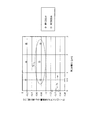
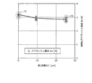
(実施例1)
次に、実施の形態1にかかる炭化珪素半導体装置n第1,2距離X1,Y1について検証した。図8は、実施例1の第1距離について検証した結果を示す特性図である。図8の横軸は第1方向Xにおけるp+型高濃度領域51からn+型ソース領域24までの第1距離X1であり、縦軸はゲート正バイアスの経時変動を観察した所定時間内で生じたゲート正バイアスの変動量ΔVgの最大値である。まず、上述した実施の形態1にかかる炭化珪素半導体装置の構造を備えたトレンチゲート構造のnチャネル型MOSFETを複数作製した(以下、実施例1とする)。実施例1の各試料は、それぞれ第1距離X1が異なる。p+型高濃度領域51’のアルミニウムドーズ量を5.15×10¹⁵/cm2とした。
(Example 1)
Next, the silicon carbide semiconductor device n first and second distances X1 and Y1 according to the first embodiment were verified. FIG. 8 is a characteristic diagram illustrating a result of verifying the first distance according to the first embodiment. The horizontal axis in FIG. 8 is the first distance X1 from the p + -type high-
これら実施例1の各試料に対して、それぞれ、200℃の高温度雰囲気下において、ソース電極31およびドレイン電極33を接地した状態で、ゲート電極28に所定の印加時間で−5Vのゲート電圧Vg(ゲート負バイアス)を印加した。そして、ゲート電極28に任意の印加時間でゲート負バイアスを印加するごとに、それぞれ室温雰囲気下においてゲート電極28にゲート正バイアスを印加して通電させて当該ゲート正バイアスを測定することで、ゲート正バイアスの初期状態時からの経時変動を1000時間観察した。ゲート電極28に印加するゲート負バイアスの印加時間は、0時間(初期状態)から1000時間に達するまで所定時間ずつ増加させた。
For each of the samples of Example 1, the gate voltage Vg of −5 V was applied to the
このゲート正バイアスの初期状態時からの経時変動の観察を、ドレイン電流Idの電流量が定格電流の千分の一の電流量Id1/I0(=10-3)となる第1測定点(図26の符号171に相当)と、ドレイン電流Idの電流量が第1測定点のドレイン電流Id1の電流量の百万分の一の電流量Id2/I0(=10-9)となる第2測定点(図26の符号172に相当)と、のそれぞれで行った。そして、第1,2測定点でのドレイン電流Idの電流量に対応するゲート正バイアスの初期状態時からの変動量ΔVgの最大値を比較した結果を図8に示す。図8において第1距離X1を0.0μmとした試料は、p+型高濃度領域151とn+型ソース領域124とが接する従来構造(図21〜25参照)に相当する。
Observation of the change over time from the initial state of the gate positive bias was performed at the first measurement point where the amount of drain current Id was 1/1000 of the rated current Id1 / I0 (= 10 -3 ) (FIG. 26, and the second measurement in which the current amount of the drain current Id is equal to the current amount Id2 / I0 (= 10 −9 ) of 1/100 of the current amount of the drain current Id1 at the first measurement point. (Corresponding to reference numeral 172 in FIG. 26). FIG. 8 shows a result of comparing the maximum value of the fluctuation amount ΔVg from the initial state of the gate positive bias corresponding to the amount of drain current Id at the first and second measurement points. In FIG. 8, the sample in which the first distance X1 is 0.0 μm corresponds to a conventional structure in which the p + -type high-
図8に示す結果より、第1,2測定点のいずれにおいても、第1方向Xにおいてp+型高濃度領域51からn+型ソース領域24までの第1距離X1を0.6μm以上とすることで、ドレイン電流Idの電流量に対応するゲート正バイアスの初期状態時からの変動量ΔVgを従来構造よりも低減することができることが確認された。ゲート正バイアスの初期状態時からの変動量ΔVgを低減するとは、ゲート正バイアスの初期状態時からの変動量ΔVgの絶対値を小さくすることである。具体的には、当該第1距離X1を0.6μm以上とすれば、例えば、第1測定点と比べてゲート正バイアスがゲートしきい値電圧Vthに近い第2測定点であっても、ドレイン電流Idの電流量に対応するゲート正バイアスの初期状態時からの変動量ΔVgを、従来構造の−1.45V(符号71で示すデータ点の試料)から−0.8V程度(符号72の円で囲むデータ点の試料)まで低減することができる。
8, the first distance X1 from the p + -type high-
図示省略するが、第2方向Yにおいてp+型高濃度領域51から最も外側のトレンチ26までの第2距離Y1を0.6μm以上とした場合においても、図8に示す結果と同様の結果が得られる。
Although not shown, even when the second distance Y1 from the p + -type high-
以上、説明したように、実施の形態1によれば、活性領域とエッジ終端領域との間の境界領域を構成するp+型高濃度領域を、第1方向にn+型ソース領域と離して、または、第2方向に最も外側のトレンチと離して、もしくはその両方と離して配置する。第1方向においてp+型高濃度領域とn+型ソース領域とに挟まれた部分、または、第2方向においてp+型高濃度領域と最も外側のトレンチとに挟まれた部分、もしくはその両方の部分は、p型炭化珪素エピタキシャル層の、半導体基板のおもて面に露出された部分である。これにより、p型ベース領域延在部の、ゲート絶縁膜に隣接する部分は、結晶欠陥が存在しないp型炭化珪素エピタキシャル層となる。このため、ゲート絶縁膜の熱酸化時に、ゲート絶縁膜に結晶欠陥に起因する正孔トラップが発生することを抑制することができる。 As described above, according to the first embodiment, the p + -type high-concentration region forming the boundary region between the active region and the edge termination region is separated from the n + -type source region in the first direction. Or in the second direction, away from the outermost trench or both. A portion sandwiched between the p + -type high-concentration region and the n + -type source region in the first direction, or a portion sandwiched between the p + -type high-concentration region and the outermost trench in the second direction, or both Is a portion of the p-type silicon carbide epitaxial layer exposed on the front surface of the semiconductor substrate. Thus, the portion of the p-type base region extension portion adjacent to the gate insulating film becomes a p-type silicon carbide epitaxial layer having no crystal defects. Therefore, generation of hole traps due to crystal defects in the gate insulating film during thermal oxidation of the gate insulating film can be suppressed.
このようにゲート絶縁膜内での正孔トラップの発生が抑制されることで、高温度条件でゲート電極にゲート負バイアスが印加されたときに、p型ベース領域の、ゲート絶縁膜との界面に正孔が蓄積されることを抑制することができる。これによって、高温度条件で、オフ状態を維持するためにゲート電極にゲート負バイアスが印加されたとしても、ドレイン電流の所定の電流量に対応するゲート正バイアスの初期状態時からの変動量を低減することができる。また、ゲート電極に0V以下のゲート電圧を印加してオフ状態を維持する際に、ドレイン遮断電流の電流量を初期状態時に近づけることができる。このため、ドレイン電流のゲインカーブが初期状態と比べてゲート電圧のマイナス方向へ変位することを抑制することができ、ゲート電圧制御による電流制御性を向上させることができる。 By suppressing the generation of hole traps in the gate insulating film in this manner, when a gate negative bias is applied to the gate electrode under high temperature conditions, the interface between the p-type base region and the gate insulating film is reduced. Holes can be suppressed from accumulating in the holes. As a result, even if a gate negative bias is applied to the gate electrode to maintain the off state under a high temperature condition, the amount of change in the gate positive bias corresponding to the predetermined amount of the drain current from the initial state is reduced. Can be reduced. In addition, when a gate voltage of 0 V or less is applied to the gate electrode to maintain the off state, the amount of drain cutoff current can be made closer to the initial state. For this reason, it is possible to suppress the gain curve of the drain current from being displaced in the negative direction of the gate voltage as compared with the initial state, and it is possible to improve the current controllability by the gate voltage control.
(実施の形態2)
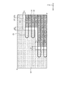
次に、実施の形態2にかかる炭化珪素半導体装置の構造について説明する。図9は、実施の形態2にかかる炭化珪素半導体装置の一部を半導体基板のおもて面側から見たレイアウトを示す平面図である。図9には、図1の頂点B,B’を対頂点とする矩形枠で囲んだ、半導体基板10のコーナー部付近における活性領域1と境界領域3との境界付近の状態を示す。半導体基板10に対する頂点Bおよび頂点B’の位置は実施の形態1と同様である。図9の切断線C−C’における断面構造は、図4の符号X1をX1’に代えたものである。図9の切断線D−D’における断面構造は、図5と同様である。
(Embodiment 2)
Next, the structure of the silicon carbide semiconductor device according to the second embodiment will be described. FIG. 9 is a plan view showing a layout of a part of the silicon carbide semiconductor device according to the second embodiment as viewed from the front side of the semiconductor substrate. FIG. 9 shows a state near the boundary between the
実施の形態2にかかる炭化珪素半導体装置が実施の形態1にかかる炭化珪素半導体装置と異なる点は、次の2点である。1つ目の相違点は、第1方向Xにおけるp+型高濃度領域51からn+型ソース領域24までの第1距離X1’を、第2方向Yにおけるp+型高濃度領域51から最も外側のトレンチ26までの第2距離Y1よりも広くした(X1’>Y1)点である。2つ目の相違点は、第1,2距離X1’,Y1の条件をともに満たすようにp+型高濃度領域51が配置される点である。第1距離X1’は例えば9.35μm以上程度とし、第2距離Y1は例えば0.6μm以上程度とするとよい。
The silicon carbide semiconductor device according to the second embodiment differs from the silicon carbide semiconductor device according to the first embodiment in the following two points. The first difference is that the first distance X1 ′ from the p + -type high-
(実施例2)
次に、実施の形態2にかかる炭化珪素半導体装置の第1,2距離X1’,Y1について検証した。図10は、実施例2の第1距離について検証した結果を示す特性図である。図10の横軸は第1方向Xにおけるp+型高濃度領域51からn+型ソース領域24までの第1距離X1’であり、縦軸はゲート正バイアスの経時変動を観察した所定時間内で生じたゲート正バイアスの変動量ΔVgの最大値である。まず、上述した実施の形態2にかかる炭化珪素半導体装置の構造を備えたトレンチゲート構造のnチャネル型MOSFETを複数作製した(以下、実施例2とする)。
(Example 2)
Next, the first and second distances X1 ′ and Y1 of the silicon carbide semiconductor device according to the second embodiment were verified. FIG. 10 is a characteristic diagram illustrating a result of verifying the first distance according to the second embodiment. The horizontal axis in FIG. 10 is the first distance X1 ′ from the p + -type high-
実施例2の各試料はそれぞれ第1距離X1’が異なる。実施例2のすべての試料はともに第2距離Y1は1.6μmとした。実施例2の各試料の定格電流は、実施例1と同じとした。p+型高濃度領域51のドーズ量は実施例1と同様である。そして、これら実施例2の各試料に対して、実施例1と同様にゲート正バイアスの初期状態時からの経時変動を第1,2測定点それぞれで観察し、ドレイン電流Idの所定の電流量に対応するゲート正バイアスの初期状態時からの変動量ΔVgの最大値を比較した結果を図10に示す。
Each sample of the second embodiment has a different first distance X1 ′. The second distance Y1 of all the samples of Example 2 was 1.6 μm. The rated current of each sample of Example 2 was the same as that of Example 1. The dose of the p + -type
図10に示す結果より、実施例2においては、第2距離Y1を1.6μmとし、第1距離X1’を9.35μm以上とした試料で、第1測定点と比べてゲート正バイアスがゲートしきい値電圧Vthに近い第2測定点であっても、第2測定点でのドレイン電流Idの電流量に対応するゲート正バイアスの初期状態時からの変動量ΔVgを−0.75V(符号73で示すデータ点の試料)から−0.4V程度(符号74の円で囲むデータ点の試料)まで低減することができることが確認された。 From the results shown in FIG. 10, in Example 2, in the sample in which the second distance Y1 was 1.6 μm and the first distance X1 ′ was 9.35 μm or more, the gate positive bias was higher than that of the first measurement point. Even at the second measurement point close to the threshold voltage Vth, the variation ΔVg from the initial state of the gate positive bias corresponding to the amount of the drain current Id at the second measurement point from the initial state is −0.75 V (sign It was confirmed that the voltage can be reduced from the sample of the data point indicated by 73) to about −0.4 V (the sample of the data point surrounded by the circle denoted by reference numeral 74).
上述したように第2距離Y1が0.6μm以上であれば、ドレイン電流Idの所定の電流量に対応するゲート正バイアスの初期状態時からの変動量ΔVgの低減効果が得られる(図9参照)。このため、実施例2において、第1距離X1’が9.35μm以上であり、かつ第2距離Y1が0.6μm以上であれば、図10に示す結果と同様に、第2測定点でのドレイン電流Idの電流量に対応するゲート正バイアスの初期状態時からの変動量ΔVgを−0.4V程度まで低減することができることがわかる。 As described above, when the second distance Y1 is 0.6 μm or more, the effect of reducing the variation ΔVg from the initial state of the gate positive bias corresponding to the predetermined amount of the drain current Id can be obtained (see FIG. 9). ). Therefore, in the second embodiment, if the first distance X1 ′ is equal to or greater than 9.35 μm and the second distance Y1 is equal to or greater than 0.6 μm, similarly to the result illustrated in FIG. It can be seen that the amount of change ΔVg from the initial state of the gate positive bias corresponding to the amount of drain current Id can be reduced to about −0.4V.
以上、説明したように、実施の形態2によれば、第1距離を第2距離よりも広くした場合においても、実施の形態1と同様の効果を得ることができる。 As described above, according to the second embodiment, the same effects as those of the first embodiment can be obtained even when the first distance is wider than the second distance.
(実施の形態3)
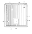
次に、実施の形態3にかかる炭化珪素半導体装置の構造について説明する。図11は、実施の形態3にかかる炭化珪素半導体装置の一部を半導体基板のおもて面側から見たレイアウトを示す平面図である。図11には、図1の頂点B,B’を対頂点とする矩形枠で囲んだ、半導体基板10のコーナー部付近における活性領域1と境界領域3との境界付近の状態を示す。半導体基板10に対する頂点Bおよび頂点B’の位置は実施の形態1と同様である。図11の切断線C−C’および切断線D−D’における断面構造は、それぞれ図4,5の符号51を51’に代えたものである。
(Embodiment 3)
Next, the structure of the silicon carbide semiconductor device according to the third embodiment will be described. FIG. 11 is a plan view showing a layout of a part of the silicon carbide semiconductor device according to the third embodiment as viewed from the front side of the semiconductor substrate. FIG. 11 shows a state near the boundary between the
実施の形態3にかかる炭化珪素半導体装置が実施の形態1にかかる炭化珪素半導体装置と異なる点は、境界領域3を構成するp+型高濃度領域51’のドーズ量を低くした点である。p+型高濃度領域51’からn+型ソース領域24までの第1距離X1が例えば0.6μm以上である場合、p+型高濃度領域51’のドーズ量は、例えばアルミニウムをドーパントとして6.4×10¹⁴/cm2以下程度であることがよい。
The silicon carbide semiconductor device according to the third embodiment differs from the silicon carbide semiconductor device according to the first embodiment in that the dose of p + -type high-
p+型高濃度領域51’のドーズ量を例えばアルミニウムをドーパントとして3.4×10¹⁴/cm2以下程度とした場合には、p+型高濃度領域51’は、従来構造(図21〜25参照)と同様にn+型ソース領域24に接していてもよい。
When the dose of the p + -type high-
(実施例3)
次に、実施の形態3にかかる炭化珪素半導体装置のp+型高濃度領域51’のドーズ量について検証した。図12は、実施例3のp+型高濃度領域のドーズ量について検証した結果を示す特性図である。図12の横軸は第1方向Xにおけるp+型高濃度領域51からn+型ソース領域24までの第1距離X1であり、縦軸はゲート正バイアスの経時変動を観察した所定時間内で生じたゲート正バイアスの変動量ΔVgの最大値である。まず、上述した実施の形態3にかかる炭化珪素半導体装置の構造を備えたトレンチゲート構造のnチャネル型MOSFETを複数作製した(以下、実施例3とする)。
(Example 3)
Next, the dose of the p + -type high-
実施例3の各第1試料81は、実施例1と同様に第1距離X1が0.6μm以上でそれぞれ異なる。上述したドレイン電流Idのゲインカーブの変位のメカニズムから、ドレイン電流Idのゲインカーブの変位は点欠陥密度にも依存することが推測される。そこで、実施例3の各第1試料81のp+型高濃度領域51’のアルミニウムドーズ量を、実施例1のp+型高濃度領域51のアルミニウムドーズ量(=5.15×10¹⁵/cm2)の1/8(=6.4×1014/cm2)とした。実施例3の各第1試料81の定格電流は実施例1と同じとした。
Each
さらに、p+型高濃度領域51’とn+型ソース領域24とを接触させた構造(すなわち第1距離X1=0μm)で、p+型高濃度領域51’のアルミニウムドーズ量を実施例1のp+型高濃度領域51のアルミニウムドーズ量の1/15(=3.4×1014/cm2)とした試料を実施例3の第2試料82とする。実施例3の第2試料82の第1距離X1およびp+型高濃度領域51のドーズ量以外の構成は、実施例3の第1試料81と同様である。
Further, in the structure in which the p + -type high-
これら実施例3の各第1,2試料81,82に対して、実施例1と同様にゲート正バイアスの初期状態時からの経時変動を第1,2測定点それぞれで観察し、第1,2測定点でのドレイン電流Idの電流量に対応するゲート正バイアスの初期状態時からの変動量ΔVgの最大値を比較した結果を図12に示す。図12では、実施例1の結果(図8参照)を「第1,2測定点」とし、実施例3の第1,2試料81,82の結果を「第1,2測定点(ドーズ量低減)」とした。
For each of the first and
図12に示す結果から、従来構造では、第2測定点でのドレイン電流Idの電流量に対応するゲート正バイアスの初期状態時からの変動量ΔVgが−1.45V(データ点71)であった。それに対して、第1距離X1を0μmとした実施例3の第2試料82であっても、第2測定点でのドレイン電流Idの電流量に対応するゲート正バイアスの初期状態時からの変動量ΔVgを−0.095Vまで低減することができることが確認された。また、第1距離X1を0.6μm以上とした実施例3の第1試料81においては、p+型高濃度領域51’のドーズ量を実施例1のp+型高濃度領域51のドーズ量の1/8のドーズ量とすることで、第2測定点でのドレイン電流Idの電流量に対応するゲート正バイアスの初期状態時からの変動量ΔVgを−0.090V〜0.098Vまで低減することができることが確認された。
From the results shown in FIG. 12, in the conventional structure, the variation ΔVg from the initial state of the gate positive bias corresponding to the amount of the drain current Id at the second measurement point from the initial state is −1.45 V (data point 71). Was. On the other hand, even in the
以上、説明したように、実施の形態3によれば、p+型高濃度領域のドーズ量を低減した場合においても、実施の形態1,2と同様の効果を得ることができる。 As described above, according to the third embodiment, the same effects as those of the first and second embodiments can be obtained even when the dose in the p + -type high-concentration region is reduced.
(実施の形態4)
次に、実施の形態4にかかる炭化珪素半導体装置の構造について説明する。図13は、実施の形態4にかかる炭化珪素半導体装置の一部を半導体基板のおもて面側から見たレイアウトを示す平面図である。図13には、図1の頂点B,B’を対頂点とする矩形枠で囲んだ、半導体基板10のコーナー部付近における活性領域1と境界領域3との境界付近の状態を示す。半導体基板10に対する頂点Bおよび頂点B’の位置は実施の形態1と同様である。図13の切断線C−C’ における断面構造は、図4の符号51,X1をそれぞれ51’、X1’に代えたものである。図13の切断線D−D’における断面構造は、図5の符号51を51’に代えたものである。
(Embodiment 4)
Next, the structure of the silicon carbide semiconductor device according to the fourth embodiment will be described. FIG. 13 is a plan view showing a layout of a part of the silicon carbide semiconductor device according to the fourth embodiment as viewed from the front side of the semiconductor substrate. FIG. 13 shows a state near the boundary between the
実施の形態4にかかる炭化珪素半導体装置が実施の形態2にかかる炭化珪素半導体装置と異なる点は、境界領域3を構成するp+型高濃度領域51’のドーズ量を実施の形態2と比べて低減した点である。すなわち、実施の形態4にかかる炭化珪素半導体装置は、実施の形態2にかかる炭化珪素半導体装置の構成に実施の形態3p+型高濃度領域51’の条件を適用したものである。第1距離X1’を例えば9.35μm以上程度とし、第2距離Y1を例えば0.6μm以上程度とする場合、p+型高濃度領域51’のドーズ量は、例えばアルミニウムをドーパントとして1.03×10¹⁵/cm2以下程度であることがよい。
The silicon carbide semiconductor device according to the fourth embodiment differs from the silicon carbide semiconductor device according to the second embodiment in that the dose of p + -type high-
(実施例4)
次に、実施の形態4にかかる炭化珪素半導体装置のp+型高濃度領域51’のドーズ量について検証した。図14は、実施例4のp+型高濃度領域のドーズ量について検証した結果を示す特性図である。図14の横軸は第1方向Xにおけるp+型高濃度領域51’からn+型ソース領域24までの第1距離X1’であり、縦軸はゲート正バイアスの経時変動を観察した所定時間内で生じたゲート正バイアスの変動量ΔVgの最大値である。まず、上述した実施の形態4にかかる炭化珪素半導体装置の構造を備えたトレンチゲート構造のnチャネル型MOSFETを複数作製した(以下、実施例4とする)。
(Example 4)
Next, the dose of the p + -type high-
まず、実施の形態4にかかる炭化珪素半導体装置の構造を備えたトレンチゲート構造のnチャネル型MOSFETを複数作製した(以下、実施例4とする)。実施例4の第1試料83の第1距離X1は、実施例2のデータ点73の試料と同様である。実施例4の第1試料83の第2距離Y1は1.6μmとした。実施例4の第1試料83のp+型高濃度領域51’のドーズ量は実施例2のp+型高濃度領域51のドーズ量(=5.15×10¹⁵/cm2)の1/8のドーズ量(=6.4×1014/cm2)とした。実施例4の第1試料83の定格電流は実施例2と同じとした。p+型高濃度領域51’を形成するためのイオン注入62のドーパントは実施例2と同様である。
First, a plurality of trench-gate n-channel MOSFETs each having the structure of the silicon carbide semiconductor device according to the fourth embodiment were manufactured (hereinafter, referred to as a fourth embodiment). The first distance X1 of the
さらに、p+型高濃度領域51’のドーズ量を実施例2のp+型高濃度領域51のドーズ量の1/5(=1.03×1015/cm2)とした試料を実施例4の第2試料84とする。実施例4の各第2試料84は、実施例2のデータ点74の各試料とでそれぞれ異なる。実施例4の第2試料84の第1距離X1およびp+型高濃度領域51’のドーズ量以外の構成は、実施例4の第1試料83と同様である。
Further, p + -type high-
これら実施例4の各第1,2試料83,84に対して、実施例2と同様にゲート正バイアスの初期状態時からの経時変動を第1,2測定点それぞれで観察し、第1,2測定点でのドレイン電流Idの電流量に対応するゲート正バイアスの初期状態時からの変動量ΔVgの最大値を比較した結果を図14に示す。図14では、実施例2の結果(図10参照)を「第1,2測定点」とし、実施例4の第1,2試料83,84の結果を「第1,2測定点(ドーズ量低減)」とした。
For each of the first and
図14に示す結果から、第2試料84においては、第2測定点でのドレイン電流Idの電流量に対応するゲート正バイアスの初期状態時からの変動量ΔVgを、実施例2で最も低減効果が得られた−0.4V程度(符号74の円で囲むデータ点の試料)から−0.085V〜0.098V程度まで低減することができることが確認された。
From the results shown in FIG. 14, in the
以上、説明したように、実施の形態4によれば、実施の形態3のp+型高濃度領域の条件を実施の形態2にかかる炭化珪素半導体装置の構成に適用した場合においても、実施の形態1,2と同様の効果を得ることができる。 As described above, according to the fourth embodiment, even when the condition of the p + -type high concentration region of the third embodiment is applied to the configuration of the silicon carbide semiconductor device according to the second embodiment, The same effects as in the first and second embodiments can be obtained.
(実施の形態5)
次に、実施の形態5にかかる炭化珪素半導体装置の構造について説明する。図15は、実施の形態5にかかる炭化珪素半導体装置の一部を半導体基板のおもて面側から見たレイアウトを示す平面図である。図15には、図1の頂点B,B’を対頂点とする矩形枠で囲んだ、半導体基板10のコーナー部付近における活性領域1と境界領域3との境界付近の状態を示す。半導体基板10に対する頂点Bおよび頂点B’の位置は実施の形態1と同様である。図15の切断線D−D’ における断面構造は、図5と同様である。図16は、図15の切断線E−E’における断面構造を示す断面図である。
(Embodiment 5)
Next, the structure of the silicon carbide semiconductor device according to the fifth embodiment will be described. FIG. 15 is a plan view showing a layout of a part of the silicon carbide semiconductor device according to the fifth embodiment as viewed from the front side of the semiconductor substrate. FIG. 15 shows a state near the boundary between the
実施の形態5にかかる炭化珪素半導体装置が実施の形態2にかかる炭化珪素半導体装置と異なる点は、活性領域1から第1方向Xに外側へ延在するトレンチ26がp+型高濃度領域51にまで達していない点である。すなわち、トレンチ26の端部は、第1方向Xにおいて、p型ベース領域延在部23’の、p+型高濃度領域51とn+型ソース領域24とに挟まれた部分で終端している。活性領域1から第1方向Xに外側へトレンチ26が延在する長さは種々変更可能であり、トレンチ26がp+型高濃度領域51に達しないように、トレンチ26を第1方向Xに外側へ延在させた分だけ、p+型高濃度領域51からn+型ソース領域24までの第1距離X11を長くすればよい。
The silicon carbide semiconductor device according to the fifth embodiment is different from the silicon carbide semiconductor device according to the second embodiment in that
実施の形態5にかかる炭化珪素半導体装置の構成に実施の形態4のp+型高濃度領域の条件を適用してもよい。 The condition of the p + -type high-concentration region of the fourth embodiment may be applied to the configuration of the silicon carbide semiconductor device according to the fifth embodiment.
以上、説明したように、実施の形態5によれば、活性領域から第1方向に外側へ延在するトレンチの終端位置によらず、実施の形態1〜4と同様の効果を得ることができる。 As described above, according to the fifth embodiment, the same effects as in the first to fourth embodiments can be obtained regardless of the termination position of the trench extending outward from the active region in the first direction. .
(実施の形態6)
次に、実施の形態6にかかる炭化珪素半導体装置の構造について説明する。図17は、実施の形態6にかかる炭化珪素半導体装置の一部を半導体基板のおもて面側から見たレイアウトを示す平面図である。図17には、図1の頂点B,B’を対頂点とする矩形枠で囲んだ、半導体基板10のコーナー部付近における活性領域1と境界領域3との境界付近の状態を示す。半導体基板10に対する頂点Bおよび頂点B’の位置は実施の形態1と同様である。図15の切断線C−C’ における断面構造は、図4と同様である。図18は、図17の切断線F−F’における断面構造を示す断面図である。
(Embodiment 6)
Next, the structure of the silicon carbide semiconductor device according to the sixth embodiment will be described. FIG. 17 is a plan view showing a layout of a part of the silicon carbide semiconductor device according to the sixth embodiment as viewed from the front side of the semiconductor substrate. FIG. 17 shows a state near the boundary between the
実施の形態6にかかる炭化珪素半導体装置が実施の形態1にかかる炭化珪素半導体装置と異なる点は、p型ベース領域延在部23’の、半導体基板10のおもて面13aに露出された部分に第2p+型コンタクト領域(第5半導体領域)25’を配置した点である。具体的には、p型ベース領域延在部23’の、第1方向Xにおいてp+型高濃度領域51とn+型ソース領域24とに挟まれた部分、または、第2方向Yにおいてp+型高濃度領域51と最も外側のトレンチ26とに挟まれた部分、もしくはその両方の部分に、第2p+型コンタクト領域25’が選択的に設けられている。
The difference between the silicon carbide semiconductor device according to the sixth embodiment and the silicon carbide semiconductor device according to the first embodiment is that p-type base
図17には、p型ベース領域延在部23’の、第2方向Yにおいてp+型高濃度領域51と最も外側のトレンチ26とに挟まれた部分にのみ、第1方向Xに所定間隔で点在する第2p+型コンタクト領域25’を設けた状態を示す。図示省略するが、p型ベース領域延在部23’の、第1方向Xにおいてp+型高濃度領域51とn+型ソース領域24とに挟まれた部分に第2p+型コンタクト領域25’を配置する場合、例えば活性領域1のp+型コンタクト領域(以下、第1p+型コンタクト領域とする)25と同じ所定間隔で、第1方向Xに第2p+型コンタクト領域25’を点在して配置すればよい。
FIG. 17 shows that only a portion of the p-type base
第2p+型コンタクト領域25’は、p+型高濃度領域51に接していてもよい。第2p+型コンタクト領域25’の条件(不純物濃度や寸法等)は、第1p+型コンタクト領域25と同様である。第2p+型コンタクト領域25’は、境界領域3において層間絶縁膜29を深さ方向Zに貫通する第3コンタクトホール29cに露出されている。第3コンタクトホール29cには、それぞれ異なる第2p+型コンタクト領域25’が露出される。第2p+型コンタクト領域25’は、第1p+型コンタクト領域25と同様、第3コンタクトホール29cにおいて金属膜30とのオーミック性を示すコンタクトを形成する。
The second p + -
ソース電極31は、第3コンタクトホール29cの内部の金属膜30を介して第2p+型コンタクト領域25’に電気的に接続され、第2p+型コンタクト領域25’を介してp型ベース領域延在部23’に電気的に接続されている。第2p+型コンタクト領域25’を設けることで、ドレイン電流Idの所定の電流量に対応するゲート電圧Vgの初期状態時からの変動量ΔVgの低減効果が若干低くなるが、p型ベース領域延在部23’のp型不純物濃度が高くなり低抵抗化されるため、アバランシェ耐量を向上させることができる。このため、ドレイン電流Idの所定電流量に対応するゲート電圧Vgの初期状態時からの変動量ΔVgと、アバランシェ耐量と、がともに所定値となるように、適宜、第2p+型コンタクト領域25’を配置すればよい。
The
実施の形態6の第2p+型コンタクト領域の構成を実施の形態2〜5にかかる炭化珪素半導体装置の構成に適用してもよい。 The configuration of the second p + -type contact region of the sixth embodiment may be applied to the configuration of the silicon carbide semiconductor device according to the second to fifth embodiments.
以上、説明したように、実施の形態6によれば、p型ベース領域延在部の、半導体基板のおもて面に露出された部分に第2p+型コンタクト領域を配置した場合においても、実施の形態1〜5と同様の効果を得ることができる。また、実施の形態6によれば、p型ベース領域延在部に第2p+型コンタクト領域を設けることによってp型ベース領域延在部が低抵抗化される。これにより、オフ時にアバランシェ降伏によりエッジ終端領域から活性領域側へ向かって流れる正孔電流(以下、アバランシェ電流とする)を、第2p+型コンタクト領域から第3コンタクトホールを介してソース電極へ向かう経路にも流すことができる。このため、アバランシェ耐量を向上させることができる。 As described above, according to the sixth embodiment, even when the second p + -type contact region is arranged in a portion of the p-type base region extension portion exposed on the front surface of the semiconductor substrate, The same effects as in the first to fifth embodiments can be obtained. According to the sixth embodiment, the resistance of the p-type base region extension is reduced by providing the second p + -type contact region in the p-type base region extension. Thereby, a hole current (hereinafter, referred to as an avalanche current) flowing from the edge termination region toward the active region due to avalanche breakdown at the time of off is directed from the second p + -type contact region to the source electrode via the third contact hole. It can also flow down the path. For this reason, the avalanche resistance can be improved.
(実施の形態7)
次に、実施の形態7にかかる炭化珪素半導体装置の構造について説明する。図19は、実施の形態7にかかる炭化珪素半導体装置を半導体基板のおもて面側から見たレイアウトを示す平面図である。実施の形態7にかかる炭化珪素半導体装置が実施の形態1にかかる炭化珪素半導体装置と異なる点は、トレンチ26’の一方の端部が活性領域1で終端している点である。例えば、第1方向Xにストライプ状に延在するトレンチ26’の組が、第1方向Xに隣り合うように活性領域1に、互いに離して2組配置されていてもよい。
(Embodiment 7)
Next, the structure of the silicon carbide semiconductor device according to the seventh embodiment will be described. FIG. 19 is a plan view showing a layout of the silicon carbide semiconductor device according to the seventh embodiment as viewed from the front side of the semiconductor substrate. The silicon carbide semiconductor device according to the seventh embodiment differs from the silicon carbide semiconductor device according to the first embodiment in that one end of
トレンチ26’の一方の端部は活性領域1の例えば中央部で終端し、他方の端部は境界領域3で終端している。活性領域1の中央部は、p+型高濃度領域で構成された無効領域4となっている。活性領域1の、無効領域4を除いた領域が有効領域である。無効領域4はMOSFETとして機能しない領域であり、有効領域はMOSFETとして機能する領域である。無効領域4のp+型高濃度領域の形成方法は、境界領域3のp+型高濃度領域と同様である。
One end of the
トレンチ26’の、活性領域1の内部で終端する一方の端部付近Hにおいても、実施の形態1と同様に、無効領域4のp+型高濃度領域はn+型ソース領域と離して配置されている。第1方向Xにおいて無効領域4のp+型高濃度領域からn+型ソース領域までの距離の条件は、第1方向Xにおいて境界領域3のp+型高濃度領域からn+型ソース領域までの第1距離と同様である。トレンチ26’の、境界領域3で終端する他方の端部付近の構成は、実施の形態1と同様である。
Also in the vicinity H of one end of
実施の形態7のトレンチの構成を実施の形態2〜6にかかる炭化珪素半導体装置の構成に適用してもよい。 The configuration of the trench of the seventh embodiment may be applied to the configuration of the silicon carbide semiconductor device according to the second to sixth embodiments.
以上、説明したように、実施の形態7によれば、トレンチゲート構造を構成するトレンチの端部に、p+型高濃度領域をn+型ソース領域と離して配置することで、実施の形態1〜6と同様の効果を得ることができる。 As described above, according to the seventh embodiment, the p + -type high-concentration region is arranged at the end of the trench forming the trench gate structure, away from the n + -type source region. The same effects as in 1 to 6 can be obtained.
(実施例5)
次に、実施の形態3にかかる炭化珪素半導体装置のドレイン遮断電流(リーク電流)Idssについて検証した。ドレイン遮断電流Idssとは、ゲート−ソース間を短絡した状態(すなわちゲート電圧Vg=0Vの状態)で、ソース−ドレイン電圧Vdを印加したときのドレイン電流Idである。まず、上述した実施の形態3にかかる炭化珪素半導体装置の構造を備えたトレンチゲート構造のnチャネル型MOSFETを作製した(以下、実施例5とする)。
(Example 5)
Next, the drain cutoff current (leakage current) Idss of the silicon carbide semiconductor device according to the third embodiment was verified. The drain cutoff current Idss is a drain current Id when the source-drain voltage Vd is applied in a state where the gate and the source are short-circuited (that is, a state where the gate voltage Vg = 0 V). First, an n-channel MOSFET having a trench gate structure having the structure of the silicon carbide semiconductor device according to the third embodiment described above was manufactured (hereinafter referred to as Example 5).
実施例5は、第1距離X1を0.6μm程度に十分長くし、p+型高濃度領域51’のアルミニウムドーズ量を従来構造よりも低く6.4×10¹⁴/cm2とし、ゲートしきい値電圧Vthを3Vと低くした。この実施例5について、ゲート電圧Vgを0Vとし、ソース−ドレイン電圧Vdを600Vとしたときのドレイン遮断電流Idssを測定した。また、比較として、従来構造(図21〜25参照)についても、実施例5と同様の条件でドレイン遮断電流Idssを測定した。
In the fifth embodiment, the first distance X1 is set sufficiently long to about 0.6 μm, the aluminum dose of the p + -type high-
従来構造では、ドレイン遮断電流Idssが時間経過とともに100pA〜100μAと大きくばらつくことが確認された。それに対して、実施例5においては、ドレイン遮断電流Idssの時間経過に伴う変動は100pA〜1nA程度であった。すなわち、p+型高濃度領域51’のアルミニウムドーズ量を低くしたとしても、ドレイン遮断電流Idssを問題にならないレベルまで小さくすることができることが確認された。
In the conventional structure, it was confirmed that the drain cut-off current Idss greatly varied from 100 pA to 100 μA with the passage of time. On the other hand, in Example 5, the variation with time of the drain cutoff current Idss was about 100 pA to 1 nA. That is, it was confirmed that even if the aluminum dose of the p + -type
実施の形態4にかかる炭化珪素半導体装置についても実施例5と同様の効果が得られる。 The same effect as that of the fifth embodiment can be obtained for the silicon carbide semiconductor device according to the fourth embodiment.
(実施例6)
次に、上述した実施の形態2にかかる炭化珪素半導体装置のオフ時に発生するアバランシェ降伏によりエッジ終端領域2から活性領域1側へ向かって流れる正孔電流(アバランシェ電流)Iavの電流量について検証した。図20は、実施例6の第1距離と規格化されたアバランシェ電流Iav/I0(I0は定格電流)との関係を示す特性図である。図20の横軸は第1方向Xにおけるp+型高濃度領域51からn+型ソース領域24までの第1距離X1’であり、縦軸は規格化アバランシェ電流Iav/I0である。
(Example 6)
Next, the amount of hole current (avalanche current) Iav flowing from the
まず、上述した実施の形態2にかかる炭化珪素半導体装置の構造を備えたトレンチゲート構造のnチャネル型MOSFETを複数作製した(以下、実施例6とする)。実施例6の各試料は、それぞれ第1距離X1を0μm、9.35μmおよび26μmとした。これら実施例6の各試料について、オフ時にアバランシェ降伏により発生するアバランシェ電流Iavを測定した。その結果を図20に示す。図20において第1距離X1’を0.0μmとした試料は、従来構造に相当する。 First, a plurality of trench-gate n-channel MOSFETs having the structure of the silicon carbide semiconductor device according to the second embodiment described above were manufactured (hereinafter referred to as Example 6). In each sample of Example 6, the first distance X1 was set to 0 μm, 9.35 μm, and 26 μm, respectively. The avalanche current Iav generated by the avalanche breakdown at the time of off was measured for each of the samples of Example 6. FIG. 20 shows the result. In FIG. 20, a sample in which the first distance X1 'is 0.0 [mu] m corresponds to a conventional structure.
図20に示す結果から、実施例6においては、規格化アバランシェ電流Iav/I0は、従来構造の3.16(符号75の円で囲むデータ点の試料)から2.84(符号76の円で囲むデータ点の試料)まで低減するが定格電流の2倍以上あり、実使用上問題にならないレベルである。 From the results shown in FIG. 20, in the sixth embodiment, the normalized avalanche current Iav / I0 is increased from 3.16 (the sample of the data point surrounded by the circle with the reference numeral 75) of the conventional structure to 2.84 (the circle with the reference numeral 76). (A sample of surrounding data points), but it is more than twice the rated current, which is a level that does not pose a problem in practical use.
図示省略するが、実施の形態1,3〜7にかかる炭化珪素半導体装置についても実施例6と同様の効果が得られる。 Although not shown, the silicon carbide semiconductor devices according to the first, third, and seventh embodiments have the same effects as those of the sixth embodiment.
以上において本発明は、上述した各実施の形態に限らず、本発明の趣旨を逸脱しない範囲で種々変更可能である。例えば、上述した各実施の形態では、MOSFETを例に説明しているが、トレンチゲート構造を有する例えばIGBT等のMOS型炭化珪素半導体装置にも適用可能である。また、本発明は、導電型(n型、p型)を反転させても同様に成り立つ。 In the above, the present invention is not limited to the above-described embodiments, and can be variously modified without departing from the spirit of the present invention. For example, in each of the embodiments described above, a MOSFET is described as an example, but the present invention is also applicable to a MOS silicon carbide semiconductor device such as an IGBT having a trench gate structure. Further, the present invention can be similarly established even when the conductivity types (n-type and p-type) are reversed.
以上のように、本発明にかかる炭化珪素半導体装置は、インバータなどの電力変換装置や種々の産業用機械などの電源装置や自動車のイグナイタなどに使用されるパワー半導体装置に有用であり、特にnチャネル型炭化珪素半導体装置に適している。 As described above, the silicon carbide semiconductor device according to the present invention is useful as a power semiconductor device used for a power conversion device such as an inverter, a power supply device for various industrial machines, an igniter of an automobile, and the like. Suitable for a channel-type silicon carbide semiconductor device.
1 活性領域
2 エッジ終端領域
3 境界領域
4 無効領域
10 半導体基板
11 n-型炭化珪素エピタキシャル層
12 p型炭化珪素エピタキシャル層
13 半導体基板のおもて面の段差
13a, 13a' 半導体基板のおもて面
13b 半導体基板のおもて面の段差のステア
13c 半導体基板のおもて面の段差のコーナー部
21 n+型出発基板
22 n-型ドリフト領域
22' n型JFET領域
23 p型ベース領域
23' p型ベース領域延在部
24 n+型ソース領域
25,25' p+型コンタクト領域
26,26' トレンチ
27 ゲート絶縁膜
28 ゲート電極
29 層間絶縁膜
29a〜29c コンタクトホール
30 金属膜
31 ソース電極
32 ゲートパッド
33 ドレイン電極
37 トレンチ直下のp+型領域
38 メサ領域のp+型領域
40 JTE構造
41,42 JTE構造のp型領域
43 n型チャネルストッパー領域
44 フィールド酸化膜
51,51' p+型高濃度領域
52 導電層
53 ゲートランナー
61 酸化膜
61a p+型コンタクト領域の形成領域
61b p+型高濃度領域の形成領域
62 イオン注入
t1 トレンチ直下のp+型領域の厚さ
t2 メサ領域ののp+型領域の厚さ
t3 境界領域のp+型高濃度領域の厚さ
t11 n-型炭化珪素エピタキシャル層の厚さ
t12 p型炭化珪素エピタキシャル層の厚さ
X 半導体基板のおもて面に平行な方向(第1方向)
X1,X1',X11 第1方向においてp+型高濃度領域からn+型ソース領域までの距離(第1距離)
Y 半導体基板のおもて面に平行で、かつ第1方向と直交する方向(第2方向)
Y1 第2方向においてp+型高濃度領域から最も外側のトレンチまでの距離(第2距離)
Z 深さ方向
DESCRIPTION OF SYMBOLS 1 Active region 2 Edge termination region 3 Boundary region 4 Invalid region 10 Semiconductor substrate 11 n - type silicon carbide epitaxial layer 12 p-type silicon carbide epitaxial layer 13 Steps 13a, 13a 'of front surface of semiconductor substrate Front surface 13b Steer of step on front surface of semiconductor substrate 13c Corner of step on front surface of semiconductor substrate 21 n + -type starting substrate 22 n -- type drift region 22 'n-type JFET region 23 p-type base region 23 'p-type base region extending portion 24 n + -type source region 25, 25' p + -type contact region 26, 26 'trench 27 gate insulating film 28 gate electrode 29 interlayer insulating film 29a-29c contact hole 30 metal film 31 source electrode 32 gate pad 33 of the p + -type region 38 mesa region right under the drain electrode 37 trench p + -type region 4 JTE structure 41 and 42 p-type region 43 n-type channel stopper region 44 field oxide film 51, 51 'p + -type high-concentration region 52 conductive layer 53 gate runner 61 oxide film 61a p + -type contact region of the formation region 61b of the JTE structure p + -type high-concentration region thickness t11 n of the p + -type high-concentration region having a thickness of t3 border region of the p + -type region of the thickness t2 mesa region of the formation region 62 p + -type region directly under the ion implantation t1 trench - type silicon carbide epitaxial layer having a thickness of t12 p-type silicon carbide epitaxial layer of thickness X semiconductor substrate in a direction parallel to the front surface (first direction)
X1, X1 ', X11 Distance from the p + -type high-concentration region to the n + -type source region in the first direction (first distance)
Y direction parallel to the front surface of the semiconductor substrate and orthogonal to the first direction (second direction)
Y1 Distance from p + -type high concentration region to outermost trench in second direction (second distance)
Z depth direction
Claims (14)
前記活性領域の周囲を囲む終端領域と、
前記半導体基板の一部をなし、前記半導体基板の前記第1主面を形成する第2導電型エピタキシャル層と、
前記活性領域において、前記第2導電型エピタキシャル層の前記第1主面側の表面層に選択的に設けられた第1導電型の第1半導体領域と、
前記活性領域と前記終端領域との境界領域において、前記第2導電型エピタキシャル層の前記第1主面側の表面層に選択的に設けられた、前記第2導電型エピタキシャル層よりも不純物濃度の高い第2導電型の第2半導体領域と、
前記第2導電型エピタキシャル層の、前記第1半導体領域および前記第2半導体領域を除いた部分である第2導電型の第3半導体領域と、
前記半導体基板の、前記第2導電型エピタキシャル層を除いた部分である第1導電型の第4半導体領域と、
前記第1半導体領域および前記第3半導体領域を貫通して前記第4半導体領域に達するトレンチと、
前記トレンチの内部にゲート絶縁膜を介して設けられたゲート電極と、
前記第1半導体領域および前記第3半導体領域に電気的に接続された第1電極と、
前記半導体基板の前記第2主面に設けられた第2電極と、
を備え、
前記第2半導体領域は、前記第1半導体領域と離して配置され、
前記第2半導体領域と前記第1半導体領域との間において前記半導体基板の前記第1主面に、前記第2導電型エピタキシャル層の前記第3半導体領域の部分が露出されていることを特徴とする炭化珪素半導体装置。 An active region through which a main current flows, provided on a semiconductor substrate of a first conductivity type having a first main surface and a second main surface;
A termination region surrounding the periphery of the active region;
A second conductivity type epitaxial layer forming a part of the semiconductor substrate and forming the first main surface of the semiconductor substrate;
A first semiconductor region of a first conductivity type selectively provided in a surface layer on the first main surface side of the second conductivity type epitaxial layer in the active region;
In a boundary region between the active region and the termination region, the second conductive type epitaxial layer has a higher impurity concentration than the second conductive type epitaxial layer selectively provided on a surface layer on the first main surface side of the second conductive type epitaxial layer. A second semiconductor region of a high second conductivity type;
A second semiconductor type third semiconductor region which is a portion of the second conductivity type epitaxial layer excluding the first semiconductor region and the second semiconductor region;
A fourth semiconductor region of a first conductivity type, which is a portion of the semiconductor substrate excluding the second conductivity type epitaxial layer;
A trench reaching the fourth semiconductor region through the first semiconductor region and the third semiconductor region;
A gate electrode provided inside the trench via a gate insulating film;
A first electrode electrically connected to the first semiconductor region and the third semiconductor region;
A second electrode provided on the second main surface of the semiconductor substrate;
With
The second semiconductor region is disposed apart from the first semiconductor region,
A portion of the third semiconductor region of the second conductivity type epitaxial layer is exposed on the first main surface of the semiconductor substrate between the second semiconductor region and the first semiconductor region. Silicon carbide semiconductor device.
前記第2半導体領域は、前記トレンチの端部付近において前記第1方向に前記第1半導体領域と離して配置されていることを特徴とする請求項1に記載の炭化珪素半導体装置。 The trench extends linearly in a first direction parallel to the first main surface of the semiconductor substrate,
2. The silicon carbide semiconductor device according to claim 1, wherein the second semiconductor region is arranged near the end of the trench in the first direction and separated from the first semiconductor region. 3.
前記第1半導体領域は、隣り合う前記トレンチの間に配置され、
前記第2半導体領域は、複数の前記トレンチのうち、前記半導体基板の前記第1主面に平行で、かつ前記第1方向と直交する第2方向に最も前記境界領域寄りの最外トレンチと離して配置され、
前記第2半導体領域と前記最外トレンチとの間において前記半導体基板の前記第1主面に、前記第2導電型エピタキシャル層の前記第3半導体領域の部分が露出されていることを特徴とする請求項2に記載の炭化珪素半導体装置。 The plurality of trenches are arranged in a stripe shape extending from the active region to the boundary region in the first direction,
The first semiconductor region is disposed between the adjacent trenches;
The second semiconductor region is separated from an outermost trench closest to the boundary region in a second direction parallel to the first main surface of the semiconductor substrate and in a second direction orthogonal to the first direction, among the plurality of trenches. Placed
A portion of the third semiconductor region of the second conductivity type epitaxial layer is exposed on the first main surface of the semiconductor substrate between the second semiconductor region and the outermost trench. The silicon carbide semiconductor device according to claim 2.
前記第1半導体領域は、隣り合う前記トレンチの間に配置され、
前記第2半導体領域は、複数の前記トレンチのうち、前記半導体基板の前記第1主面に平行で、かつ前記第1方向と直交する第2方向に最も前記境界領域寄りの最外トレンチと離して配置され、
前記第2半導体領域と前記最外トレンチとの間において前記半導体基板の前記第1主面に、前記第2導電型エピタキシャル層の前記第3半導体領域の部分が露出されていることを特徴とする請求項1に記載の炭化珪素半導体装置。 A plurality of the trenches are arranged in a stripe shape extending from the active region to the boundary region in a first direction parallel to the first main surface of the semiconductor substrate;
The first semiconductor region is disposed between the adjacent trenches;
The second semiconductor region is separated from an outermost trench closest to the boundary region in a second direction parallel to the first main surface of the semiconductor substrate and in a second direction orthogonal to the first direction, among the plurality of trenches. Placed
A portion of the third semiconductor region of the second conductivity type epitaxial layer is exposed on the first main surface of the semiconductor substrate between the second semiconductor region and the outermost trench. The silicon carbide semiconductor device according to claim 1.
前記第3半導体領域は、前記第5半導体領域を介して前記第1電極に電気的に接続されていることを特徴とする請求項1〜11のいずれか一つに記載の炭化珪素半導体装置。 A second conductive type fifth semiconductor region having a higher impurity concentration than the third semiconductor region, selectively provided in a portion of the third semiconductor region exposed on the first main surface of the semiconductor substrate; Prepare,
The silicon carbide semiconductor device according to claim 1, wherein the third semiconductor region is electrically connected to the first electrode via the fifth semiconductor region.
Priority Applications (3)
| Application Number | Priority Date | Filing Date | Title |
|---|---|---|---|
| JP2018123719A JP7127389B2 (en) | 2018-06-28 | 2018-06-28 | Silicon carbide semiconductor device |
| US16/389,276 US10886371B2 (en) | 2018-06-28 | 2019-04-19 | Silicon carbide semiconductor device |
| CN201910337866.4A CN110660858B (en) | 2018-06-28 | 2019-04-25 | Silicon carbide semiconductor device |
Applications Claiming Priority (1)
| Application Number | Priority Date | Filing Date | Title |
|---|---|---|---|
| JP2018123719A JP7127389B2 (en) | 2018-06-28 | 2018-06-28 | Silicon carbide semiconductor device |
Publications (2)
| Publication Number | Publication Date |
|---|---|
| JP2020004876A true JP2020004876A (en) | 2020-01-09 |
| JP7127389B2 JP7127389B2 (en) | 2022-08-30 |
Family
ID=69008329
Family Applications (1)
| Application Number | Title | Priority Date | Filing Date |
|---|---|---|---|
| JP2018123719A Active JP7127389B2 (en) | 2018-06-28 | 2018-06-28 | Silicon carbide semiconductor device |
Country Status (3)
| Country | Link |
|---|---|
| US (1) | US10886371B2 (en) |
| JP (1) | JP7127389B2 (en) |
| CN (1) | CN110660858B (en) |
Cited By (3)
| Publication number | Priority date | Publication date | Assignee | Title |
|---|---|---|---|---|
| JP2023088816A (en) * | 2021-12-15 | 2023-06-27 | 富士電機株式会社 | Silicon carbide semiconductor device |
| JP2023138080A (en) * | 2022-03-18 | 2023-09-29 | 富士電機株式会社 | silicon carbide semiconductor device |
| JP7835034B2 (en) | 2021-12-15 | 2026-03-25 | 富士電機株式会社 | Silicon carbide semiconductor equipment |
Families Citing this family (6)
| Publication number | Priority date | Publication date | Assignee | Title |
|---|---|---|---|---|
| JP7127389B2 (en) * | 2018-06-28 | 2022-08-30 | 富士電機株式会社 | Silicon carbide semiconductor device |
| US11158703B2 (en) * | 2019-06-05 | 2021-10-26 | Microchip Technology Inc. | Space efficient high-voltage termination and process for fabricating same |
| JP7512624B2 (en) * | 2020-03-17 | 2024-07-09 | 富士電機株式会社 | Silicon carbide semiconductor device |
| JP7207361B2 (en) * | 2020-04-22 | 2023-01-18 | 株式会社デンソー | semiconductor equipment |
| US20220157951A1 (en) * | 2020-11-17 | 2022-05-19 | Hamza Yilmaz | High voltage edge termination structure for power semicondcutor devices and manufacturing method thereof |
| JP7506628B2 (en) * | 2021-03-24 | 2024-06-26 | 株式会社東芝 | Semiconductor Device |
Citations (8)
| Publication number | Priority date | Publication date | Assignee | Title |
|---|---|---|---|---|
| JPH1117176A (en) * | 1997-06-24 | 1999-01-22 | Hitachi Ltd | Silicon carbide semiconductor device |
| JP2006135150A (en) * | 2004-11-08 | 2006-05-25 | Denso Corp | Silicon carbide semiconductor device and manufacturing method thereof |
| JP2010147222A (en) * | 2008-12-18 | 2010-07-01 | Denso Corp | Silicon carbide semiconductor device and method of manufacturing the same |
| JP2015126192A (en) * | 2013-12-27 | 2015-07-06 | 株式会社豊田中央研究所 | Vertical semiconductor device |
| JP2015220334A (en) * | 2014-05-16 | 2015-12-07 | ローム株式会社 | Semiconductor device |
| JP2018019045A (en) * | 2016-07-29 | 2018-02-01 | 富士電機株式会社 | Silicon carbide semiconductor device and silicon carbide semiconductor device manufacturing method |
| JP2018046162A (en) * | 2016-09-14 | 2018-03-22 | 富士電機株式会社 | Silicon carbide semiconductor device |
| JP2018082056A (en) * | 2016-11-16 | 2018-05-24 | 富士電機株式会社 | Semiconductor device and method of manufacturing the same |
Family Cites Families (7)
| Publication number | Priority date | Publication date | Assignee | Title |
|---|---|---|---|---|
| JP6183087B2 (en) * | 2013-09-13 | 2017-08-23 | 富士電機株式会社 | Silicon carbide semiconductor device and method for manufacturing silicon carbide semiconductor device |
| US9761702B2 (en) * | 2014-02-04 | 2017-09-12 | MaxPower Semiconductor | Power MOSFET having planar channel, vertical current path, and top drain electrode |
| US10453951B2 (en) * | 2014-09-26 | 2019-10-22 | Mitsubishi Electric Corporation | Semiconductor device having a gate trench and an outside trench |
| KR101970087B1 (en) * | 2015-01-27 | 2019-04-17 | 미쓰비시덴키 가부시키가이샤 | Semiconductor device |
| DE112016003509B4 (en) * | 2015-10-16 | 2023-07-20 | Fuji Electric Co., Ltd. | Semiconductor device and method of manufacturing a semiconductor device |
| JP6848316B2 (en) * | 2016-10-05 | 2021-03-24 | 富士電機株式会社 | Semiconductor devices and methods for manufacturing semiconductor devices |
| JP7127389B2 (en) * | 2018-06-28 | 2022-08-30 | 富士電機株式会社 | Silicon carbide semiconductor device |
-
2018
- 2018-06-28 JP JP2018123719A patent/JP7127389B2/en active Active
-
2019
- 2019-04-19 US US16/389,276 patent/US10886371B2/en active Active
- 2019-04-25 CN CN201910337866.4A patent/CN110660858B/en active Active
Patent Citations (8)
| Publication number | Priority date | Publication date | Assignee | Title |
|---|---|---|---|---|
| JPH1117176A (en) * | 1997-06-24 | 1999-01-22 | Hitachi Ltd | Silicon carbide semiconductor device |
| JP2006135150A (en) * | 2004-11-08 | 2006-05-25 | Denso Corp | Silicon carbide semiconductor device and manufacturing method thereof |
| JP2010147222A (en) * | 2008-12-18 | 2010-07-01 | Denso Corp | Silicon carbide semiconductor device and method of manufacturing the same |
| JP2015126192A (en) * | 2013-12-27 | 2015-07-06 | 株式会社豊田中央研究所 | Vertical semiconductor device |
| JP2015220334A (en) * | 2014-05-16 | 2015-12-07 | ローム株式会社 | Semiconductor device |
| JP2018019045A (en) * | 2016-07-29 | 2018-02-01 | 富士電機株式会社 | Silicon carbide semiconductor device and silicon carbide semiconductor device manufacturing method |
| JP2018046162A (en) * | 2016-09-14 | 2018-03-22 | 富士電機株式会社 | Silicon carbide semiconductor device |
| JP2018082056A (en) * | 2016-11-16 | 2018-05-24 | 富士電機株式会社 | Semiconductor device and method of manufacturing the same |
Cited By (4)
| Publication number | Priority date | Publication date | Assignee | Title |
|---|---|---|---|---|
| JP2023088816A (en) * | 2021-12-15 | 2023-06-27 | 富士電機株式会社 | Silicon carbide semiconductor device |
| JP7835034B2 (en) | 2021-12-15 | 2026-03-25 | 富士電機株式会社 | Silicon carbide semiconductor equipment |
| JP2023138080A (en) * | 2022-03-18 | 2023-09-29 | 富士電機株式会社 | silicon carbide semiconductor device |
| JP7800239B2 (en) | 2022-03-18 | 2026-01-16 | 富士電機株式会社 | Silicon carbide semiconductor device |
Also Published As
| Publication number | Publication date |
|---|---|
| CN110660858B (en) | 2025-02-25 |
| CN110660858A (en) | 2020-01-07 |
| US10886371B2 (en) | 2021-01-05 |
| US20200006494A1 (en) | 2020-01-02 |
| JP7127389B2 (en) | 2022-08-30 |
Similar Documents
| Publication | Publication Date | Title |
|---|---|---|
| JP7127389B2 (en) | Silicon carbide semiconductor device | |
| JP7059555B2 (en) | Semiconductor device | |
| CN102163621B (en) | The method of semiconductor device and manufacture semiconductor device | |
| US10903202B2 (en) | Semiconductor device | |
| US10109725B2 (en) | Reverse-conducting semiconductor device | |
| JP2001339063A (en) | Semiconductor device and method of manufacturing the same | |
| CN107833921B (en) | Switching device and method of manufacturing switching device | |
| CN114725219B (en) | Silicon carbide trench gate transistor and method of manufacturing the same | |
| JP7611944B2 (en) | Power device with hybrid gate structure | |
| JP2020177973A (en) | Semiconductor device | |
| JP2002231944A (en) | Power semiconductor device | |
| SE513284C3 (en) | Semiconductor component with linear current-to-voltage characteristics | |
| CN114843346B (en) | Low-resistance trench type silicon carbide transistor and manufacturing method thereof | |
| JP2026027463A (en) | 4H-SiC electronic device with improved short circuit performance and method for manufacturing same | |
| JP2011243915A (en) | Semiconductor device and method of manufacturing the same | |
| JP6299658B2 (en) | Insulated gate type switching element | |
| CN104253152A (en) | IGBT (insulated gate bipolar transistor) and manufacturing method thereof | |
| KR100910798B1 (en) | High voltage trench isolation gate bipolar transistor having trenches with impurity implantation layers formed therein and a method of manufacturing the same | |
| US9245986B2 (en) | Power semiconductor device and method of manufacturing the same | |
| CN112802897B (en) | 4H-SIC MOSFET device and its manufacturing method | |
| JP2015153988A (en) | semiconductor device | |
| JP2019140159A (en) | Semiconductor device and method of manufacturing semiconductor device | |
| JP3916874B2 (en) | Semiconductor device | |
| JP2016025324A (en) | Semiconductor device and control method for the same | |
| JP2015142073A (en) | semiconductor device |
Legal Events
| Date | Code | Title | Description |
|---|---|---|---|
| A621 | Written request for application examination |
Free format text: JAPANESE INTERMEDIATE CODE: A621 Effective date: 20210514 |
|
| A977 | Report on retrieval |
Free format text: JAPANESE INTERMEDIATE CODE: A971007 Effective date: 20220310 |
|
| A131 | Notification of reasons for refusal |
Free format text: JAPANESE INTERMEDIATE CODE: A131 Effective date: 20220315 |
|
| A521 | Request for written amendment filed |
Free format text: JAPANESE INTERMEDIATE CODE: A523 Effective date: 20220422 |
|
| TRDD | Decision of grant or rejection written | ||
| A01 | Written decision to grant a patent or to grant a registration (utility model) |
Free format text: JAPANESE INTERMEDIATE CODE: A01 Effective date: 20220719 |
|
| A61 | First payment of annual fees (during grant procedure) |
Free format text: JAPANESE INTERMEDIATE CODE: A61 Effective date: 20220801 |
|
| R150 | Certificate of patent or registration of utility model |
Ref document number: 7127389 Country of ref document: JP Free format text: JAPANESE INTERMEDIATE CODE: R150 |
|
| R250 | Receipt of annual fees |
Free format text: JAPANESE INTERMEDIATE CODE: R250 |