JP2019180621A - Game machine - Google Patents
Game machine Download PDFInfo
- Publication number
- JP2019180621A JP2019180621A JP2018072828A JP2018072828A JP2019180621A JP 2019180621 A JP2019180621 A JP 2019180621A JP 2018072828 A JP2018072828 A JP 2018072828A JP 2018072828 A JP2018072828 A JP 2018072828A JP 2019180621 A JP2019180621 A JP 2019180621A
- Authority
- JP
- Japan
- Prior art keywords
- wiring
- signal
- power supply
- pattern
- shape
- Prior art date
- Legal status (The legal status is an assumption and is not a legal conclusion. Google has not performed a legal analysis and makes no representation as to the accuracy of the status listed.)
- Pending
Links
Images


Abstract
Description
本発明は、遊技を行うことが可能な遊技機に関する。 The present invention relates to a gaming machine capable of playing a game.
従来、複数の電子部品が実装された基板を備える遊技機において、基板に実装されているROMの管理情報が記されたシールを、基板を構成するフレキシブル基板に貼付したものがある(例えば、特許文献1参照)。 2. Description of the Related Art Conventionally, in a gaming machine including a board on which a plurality of electronic components are mounted, there is one in which a sticker on which management information of a ROM mounted on a board is written is attached to a flexible board constituting the board (for example, a patent Reference 1).
しかしながら、特許文献1にあっては、遊技機の製造時における搬送工程や基板を組み付ける工程等において、シールの縁部に物が接触する等によって、シールが剥がれたり、位置がずれたり、或いは一部が離れて折れ曲がってしまうことがあり、該シールに記されている情報の確認や読み取りを良好に行うことができなくなってしまうという問題があった。
However, in
本発明は、このような問題点に着目してなされたもので、シールに記されている情報の確認や読み取りを良好に行うことができなくなってしまうことを防ぐことのできる遊技機を提供することを目的とする。 The present invention has been made paying attention to such problems, and provides a gaming machine capable of preventing a situation in which confirmation and reading of information written on a sticker cannot be performed satisfactorily. For the purpose.
前記課題を解決するために、本発明の手段1に記載の遊技機は、
遊技を行うことが可能な遊技機(例えば、パチンコ遊技機1)であって、
複数の電子部品(例えば、演出制御用CPU120、ROM121、RAM122等)が実装された基板(例えば、演出制御基板12)を備え、
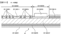
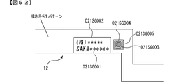
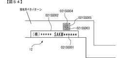
前記基板は、当該基板に関する情報が読み取り可能に記されたシールが貼着されるシール貼着部(例えば、製造日やロット番号やシリアル番号等の第2情報が読み取り可能にシンボル化された二次元バーコードが印刷されたシール021SG003が貼着される第2情報表示部021SG004)を有し、
前記シール貼着部は、基板上に形成された配線パターン及び接地パターンとは異なる部分に設けられている(例えば、第2情報表示部021SG004は、配線パターンや接地用ベタパターンを構成する銅箔021SG010がエッチングによって除去されることで、配線パターンや接地用ベタパターンが形成されていない部分に設けられている)
ことを特徴としている。
この特徴によれば、シールに記されている基板に関する情報の確認や読み取りを良好に行うことができなくなってしまうことを防ぐことができる。
In order to solve the above-described problem, a gaming machine according to
A gaming machine capable of performing a game (for example, a pachinko gaming machine 1),
Provided with a board (for example, effect control board 12) on which a plurality of electronic components (for example,
The board has a sticker pasted with a sticker on which information about the board is readable (for example, second information such as a manufacturing date, a lot number, a serial number, etc. is symbolized so that it can be read. A second information display unit 021SG004) to which a sticker 021SG003 printed with a dimension barcode is attached,
The seal sticking portion is provided in a portion different from the wiring pattern and the ground pattern formed on the substrate (for example, the second information display portion 021SG004 is a copper foil constituting the wiring pattern or the ground solid pattern). (021SG010 is removed by etching so that the wiring pattern and the grounding solid pattern are not formed)
It is characterized by that.
According to this feature, it is possible to prevent the information related to the substrate written on the sticker from being properly confirmed and read.
本発明の手段2の遊技機は、手段1に記載の遊技機であって、
前記シール貼着部は、前記配線パターン及び前記接地パターンを構成する導電材が形成されていない部分である(例えば、第2情報表示部021SG004は、図50に示すように、配線パターンや接地用ベタパターンを構成する銅箔021SG010がエッチングによって除去されて凹んだ部分である)
ことを特徴としている。
この特徴によれば、シール貼着部が、導電材の厚み分だけ凹んだ部分となるので、基板に関する情報の確認や読み取りを良好に行うことができなくなってしまうことを、より一層防ぐことができる。
The gaming machine of
The seal sticking portion is a portion where the conductive material constituting the wiring pattern and the ground pattern is not formed (for example, the second information display portion 021SG004 has a wiring pattern or grounding portion as shown in FIG. 50). (The copper foil 021SG010 constituting the solid pattern is removed by etching and is a recessed portion)
It is characterized by that.
According to this feature, since the sticking portion of the seal is a portion that is recessed by the thickness of the conductive material, it is possible to further prevent the information related to the substrate from being unable to be confirmed and read satisfactorily. it can.
本発明の手段3の遊技機は、手段1または手段2に記載の遊技機であって、
前記シール貼着部は、前記基板の1の面のみに設けられている(例えば、第2情報表示部021SG004は、演出制御基板12の表面(部品実装面)のみに設けられている)
ことを特徴としている。
この特徴によれば、1の面のみにシールを貼着するだけでよいので、シール貼着部を設けるための負荷を低減できる。
The gaming machine of
The seal sticking portion is provided only on one surface of the substrate (for example, the second information display portion 021SG004 is provided only on the surface (component mounting surface) of the effect control substrate 12).
It is characterized by that.
According to this feature, since it is only necessary to stick the seal on only one surface, the load for providing the seal attaching portion can be reduced.
本発明の手段4の遊技機は、手段1〜手段3のいずれかに記載の遊技機であって、
前記基板(例えば、演出制御基板12)は、前記シールに記された情報とは異なる情報であって、当該基板を識別するための識別情報(例えば、製造会社名と型式IDとから成る第1情報)が読み取り可能に表示された識別情報表示部(例えば、第1情報表示部021SG002)を有し、
前記識別情報表示部は、前記シール貼着部の近傍に設けられている(例えば、図49において、第1情報表示部021SG002が、第2情報表示部021SG004に隣接して設けられている)
ことを特徴としている。
この特徴によれば、基板に関する情報と識別情報の読み取り効率を向上できる。
The gaming machine of
The board (for example, the production control board 12) is information different from the information written on the sticker, and includes identification information for identifying the board (for example, a first name consisting of a manufacturer name and a model ID). Information) is displayed in a readable manner (for example, the first information display unit 021SG002),
The identification information display part is provided in the vicinity of the sticker sticking part (for example, in FIG. 49, the first information display part 021SG002 is provided adjacent to the second information display part 021SG004).
It is characterized by that.
According to this feature, it is possible to improve the reading efficiency of information on the substrate and identification information.
本発明の手段5の遊技機は、手段4に記載の遊技機であって、
前記識別情報表示部は、前記基板の表裏面の双方に設けられている(例えば、第1情報表示部021SG002における第1情報021SG001と同一の記号021SG006が、演出制御基板12の裏面側に設けられた第3情報表示部021SG007に記されている)
ことを特徴としている。
この特徴によれば、基板の表裏面のいずれにおいても、第1情報を確認することができる。
The gaming machine of
The identification information display unit is provided on both the front and back surfaces of the substrate (for example, the same symbol 021SG006 as the first information 021SG001 in the first information display unit 021SG002 is provided on the back side of the
It is characterized by that.
According to this feature, the first information can be confirmed on both the front and back surfaces of the substrate.
本発明の手段6の遊技機は、手段4または手段5に記載の遊技機であって、
前記シール貼着部と前記識別情報表示部とは、前記基板の同一辺に沿って並んで設けられている(例えば、第2情報表示部021SG004と第1情報表示部021SG002とが、図49に示すように、演出制御基板12の切り欠きを有する外周辺に沿って並んで設けられている)
ことを特徴としている。
この特徴によれば、基板に関する情報と識別情報とを認識し易くでき、的確な読み取りを行うことができる。
The gaming machine of means 6 of the present invention is the gaming machine according to
The seal sticking part and the identification information display part are provided side by side along the same side of the substrate (for example, the second information display part 021SG004 and the first information display part 021SG002 are shown in FIG. As shown, the
It is characterized by that.
According to this feature, it is possible to easily recognize the information about the substrate and the identification information and perform accurate reading.
本発明の手段7の遊技機は、手段4〜手段6のいずれかに記載の遊技機であって、
前記シール貼着部と前記識別情報表示部との間には、電子部品が実装されていない(例えば、第2情報表示部021SG004と第1情報表示部021SG002との境界に位置する銅箔021SG010が全てエッチングされて除去されていることで、図49並びに図50に示すように、該境界には、いずれの電子部品も実装されていない部分)
ことを特徴としている。
この特徴によれば、基板に関する情報と識別情報の読み取りが、電子部品に邪魔されてしまうことを防ぐことができる。
A gaming machine of means 7 of the present invention is the gaming machine according to any one of
No electronic component is mounted between the seal sticking part and the identification information display part (for example, the copper foil 021SG010 located at the boundary between the second information display part 021SG004 and the first information display part 021SG002) (Each part is not mounted with any electronic component at the boundary, as shown in FIGS. 49 and 50).
It is characterized by that.
According to this feature, reading of information related to the substrate and identification information can be prevented from being disturbed by electronic components.
本発明の手段8の遊技機は、手段4〜手段7のいずれかに記載の遊技機であって、
前記基板(例えば、演出制御基板12)が収納されている基板ケース(例えば、基板ケース800)を備え、
前記シール貼着部と前記識別情報表示部とは、前記基板が前記基板ケースに収納されている状態においても、前記基板ケースの外側から視認可能である(例えば、基板ケース800の外部から、基板ケース800の内部に収納されている演出制御基板12における第1情報表示部021SG002と第2情報表示部021SG004とを視認可能である)
ことを特徴としている。
この特徴によれば、基板ケースの外側から、基板に関する情報と識別情報を読み取ることができる。
The gaming machine of
A substrate case (for example, substrate case 800) in which the substrate (for example, the production control substrate 12) is stored;
The seal sticking portion and the identification information display portion are visible from the outside of the substrate case even when the substrate is housed in the substrate case (for example, from the outside of the
It is characterized by that.
According to this feature, information on the substrate and identification information can be read from the outside of the substrate case.
尚、本発明は、本発明の請求項に記載された発明特定事項のみを有するものであって良いし、本発明の請求項に記載された発明特定事項とともに該発明特定事項以外の構成を有するものであってもよい。 In addition, this invention may have only the invention specific matter described in the claim of this invention, and has a structure other than this invention specific matter with the invention specific matter described in the claim of this invention. It may be a thing.
図1は、この実施の形態に係るパチンコ遊技機1の正面図である。パチンコ遊技機1は、遊技盤2と、遊技機用枠3とを備えている。その他、パチンコ遊技機1は、遊技機用枠3を回動可能に支持する外枠などを備えている。遊技盤2は、遊技盤面を構成するゲージ盤である。遊技機用枠3は、遊技盤2を固定する台枠である。遊技盤2には、ガイドレールなどによって囲まれた遊技領域が形成されている。発射装置から発射された遊技球(遊技媒体)は、発射通路を通過して、遊技領域に打ち込まれる。遊技機用枠3には、ガラス窓を有するガラス扉枠が回動可能に設けられている。
FIG. 1 is a front view of a
遊技盤2の所定位置には、第1特別図柄表示装置4A、第2特別図柄表示装置4B、画像表示装置5、普通入賞球装置6A、普通可変入賞球装置6B、特別可変入賞球装置7、普通図柄表示器20、第1保留表示器25A、第2保留表示器25B、普図保留表示器25C、通過ゲート41などが設けられている。その他、遊技領域における遊技盤面には、風車や多数の障害釘、一般入賞口、アウト口などが設けられていればよい。遊技領域の周辺部には遊技効果ランプ9が設けられている。遊技機用枠3の左右上部位置にはスピーカ8L、8Rが設けられている。
At predetermined positions on the
遊技機用枠3の右下部位置には、打球操作ハンドル(操作ノブ)が設けられている。打球操作ハンドルは、遊技球を遊技領域に向けて発射するために遊技者等によって操作され、その操作量(回転量)に応じて遊技球の弾発力が調整される。遊技領域の下方における遊技機用枠3の所定位置には、遊技球を保持(貯留)する上皿(打球供給皿)と、上皿からの余剰球などを保持(貯留)する下皿が設けられている。下皿を形成する部材にはスティックコントローラ31Aが取り付けられ、上皿を形成する部材にはプッシュボタン31Bが設けられている。
A hitting operation handle (operation knob) is provided at the lower right position of the
第1特別図柄表示装置4A、第2特別図柄表示装置4B、画像表示装置5の画面上などでは、特別図柄や飾り図柄の可変表示が行われる。これらの可変表示は、普通入賞球装置6Aに形成された第1始動入賞口を遊技球が通過(進入)したことによる第1始動入賞の発生に基づいて、あるいは、普通可変入賞球装置6Bに形成された第2始動入賞口を遊技球が通過(進入)したことによる第2始動入賞の発生に基づいて、実行可能となる。第1特別図柄表示装置4Aと第2特別図柄表示装置4Bはそれぞれ、例えば7セグメントやドットマトリクスのLED(発光ダイオード)などを用いて構成され、可変表示ゲームの一例となる特図ゲームにおいて、識別情報(特別識別情報)である特別図柄(特図)が、変動可能に表示(可変表示)される。画像表示装置5は、例えばLCD(液晶表示装置)などを用いて構成され、各種の演出画像を表示する表示領域を形成している。画像表示装置5の画面上では、特図ゲームにおける第1特別図柄表示装置4Aによる特別図柄(第1特図)の可変表示や第2特別図柄表示装置4Bによる特別図柄(第2特図)の可変表示のそれぞれに対応して、例えば3つといった複数の可変表示部となる飾り図柄表示エリアにて、識別情報(装飾識別情報)である飾り図柄が可変表示される。この飾り図柄の可変表示も、可変表示ゲームに含まれる。一例として、画像表示装置5の画面上には、「左」、「中」、「右」の飾り図柄表示エリア5L、5C、5Rが配置されている。
On the screens of the first special
画像表示装置5の画面上には、保留記憶表示エリア5Hが配置されている。保留記憶表示エリア5Hでは、特図ゲームに対応した可変表示の保留数(特図保留記憶数)を特定可能に表示する保留表示が行われる。保留表示は、可変表示に関する情報の保留記憶に対応して表示可能なものであればよい。保留記憶表示エリア5Hとともに、あるいは、保留記憶表示エリア5Hに代えて、第1保留表示器25Aと第2保留表示器25Bとを用いた保留表示が行われてもよい。
On the screen of the
図2は、各種基板や周辺装置などの構成例を示すブロック図である。パチンコ遊技機1には、例えば図2に示すような主基板11、演出制御基板12、音声制御基板13、ランプ制御基板14といった、各種制御基板が搭載されている。また、パチンコ遊技機1には、中継基板15、ドライバ基板19、電源基板92なども搭載されている。その他にも、例えば払出制御基板、情報端子基板、発射制御基板、インタフェース基板、タッチセンサ基板などといった、各種の基板が搭載されてもよい。各種制御基板は、導体パターンが形成されて電気部品が実装されるプリント配線板などの電子回路基板だけではなく、電子回路基板に電気部品が実装(搭載)されて特定の電気的機能を実現するように構成された電子回路実装基板を含む概念である。
FIG. 2 is a block diagram illustrating a configuration example of various substrates and peripheral devices. The
電源基板92は、外部電源(商用電源)である交流電源からの電力を、主基板11や演出制御基板12などの各種制御基板を含めた電気部品に供給可能となるように構成されている。電源基板92は、例えば交流(AC)を直流(DC)に変換するための整流回路、所定の直流電圧を特定の直流電圧(例えば直流12Vや直流5Vなど)に変換するための電源回路などを、備えている。電源基板92にて生成された電圧は、ドロア中継基板を介して主基板11や演出制御基板12などに供給されてもよい。
The
主基板11には、遊技制御用マイクロコンピュータ100、スイッチ回路110、ソレノイド回路111などが搭載されている。主基板11では、ゲートスイッチ21、始動口スイッチ(第1始動口スイッチ22Aおよび第2始動口スイッチ22B)、カウントスイッチ23といった、各種検出用のスイッチから取り込んだ信号が、スイッチ回路110を介して遊技制御用マイクロコンピュータ100に伝送される。ゲートスイッチ21は、通過ゲート41を通過した遊技球(ゲート通過球)を検出する。ゲートスイッチ21によるゲート通過球の検出に基づいて、普通図柄表示器20による普通図柄の可変表示が実行可能となる。第1始動口スイッチ22Aは、第1始動入賞口を通過(進入)した遊技球を検出する。第2始動口スイッチ22Bは、第2始動入賞口を通過(進入)した遊技球を検出する。カウントスイッチ23は、大入賞口を通過(進入)した遊技球を検出する。第1始動入賞口や第2始動入賞口、大入賞口といった、各種の入賞口を通過した遊技球が検出された場合には、それぞれの入賞口に対応して予め個数が定められた賞球としての遊技球が払い出される。
On the
主基板11では、遊技制御用マイクロコンピュータ100からのソレノイド駆動信号が、ソレノイド回路111を介して普通電動役物用のソレノイド81や大入賞口扉用のソレノイド82に伝送される。普通電動役物用のソレノイド81は、普通可変入賞球装置6Bに形成された第2始動入賞口を遊技球が通過しにくい状態(または通過しない状態)と通過しやすい状態(または通過する状態)とに変化可能にする。大入賞口扉用のソレノイド82は、特別可変入賞球装置7に形成された大入賞口を遊技球が通過不可能な状態と通過可能な状態とに変化可能にする。主基板11からは、第1特別図柄表示装置4A、第2特別図柄表示装置4B、普通図柄表示器20などの表示制御を行うための指令信号が伝送される。
On the
主基板11に搭載された遊技制御用マイクロコンピュータ100は、例えば1チップのマイクロコンピュータであり、遊技制御用のプログラムや固定データ等を記憶するROM101と、遊技制御用のワークエリアを提供するRAM102と、遊技制御用のプログラムを実行して制御動作を行うCPU103と、CPU103とは独立して乱数値を示す数値データの更新を行う乱数回路104と、I/O(Input/Output port)105とを備えて構成される。一例として、遊技制御用マイクロコンピュータ100では、CPU103がROM101から読み出したプログラムを実行することにより、パチンコ遊技機1における遊技の進行を制御するための処理が実行される。主基板11に搭載された遊技制御用マイクロコンピュータ100では、例えば乱数回路104やRAM102の所定領域に設けられた遊技用ランダムカウンタなどにより、遊技の進行を制御するために用いられる各種の乱数値を示す数値データが更新可能にカウント(生成)される。遊技の進行を制御するために用いられる乱数は、遊技用乱数ともいう。
The
演出制御基板12は、中継基板15を介して主基板11から伝送された制御信号(演出制御コマンド)の受信に基づいて、画像表示装置5、スピーカ8L、8R、遊技効果ランプ9、演出用モータ60および演出用LED61といった演出用の電気部品による演出動作を制御可能とする。演出制御基板12には、演出制御用CPU120やROM121、RAM122、表示制御部123、乱数回路124、I/O125などが搭載されている。
The
演出制御基板12に搭載された演出制御用CPU120は、ROM121から読み出した演出制御用のプログラムや固定データ等を用いて、演出用の電気部品による演出動作を制御するための処理を実行する。演出制御基板12に搭載された表示制御部123は、演出制御用CPU120からの表示制御指令などに基づき、画像表示装置5における表示動作の制御内容を決定する。例えば、表示制御部123は、画像表示装置5の表示画面内に表示させる演出画像の切換タイミングを決定することなどにより、飾り図柄の可変表示や各種の演出表示を実行させるための制御を行う。
The
演出制御基板12には、コントローラセンサユニット35Aと、プッシュセンサ35Bとが接続されている。コントローラセンサユニット35Aは、傾倒方向センサと、トリガセンサとを含んでいる。傾倒方向センサは、スティックコントローラ31Aの操作桿に対する傾倒操作が行われたときに、複数のセンサを用いて操作桿の傾倒方向を検出可能にする。トリガセンサは、スティックコントローラ31Aの操作桿に設けられたトリガボタンに対する押引操作の有無を検出可能にする。すなわち、コントローラセンサユニット35Aにより、スティックコントローラ31Aの操作桿に対する傾倒動作やトリガボタンに対する押引動作といった、スティックコントローラ31Aを用いた遊技者の動作を検出することができる。プッシュセンサ35Bにより、プッシュボタン31Bに対する押下動作といった、プッシュボタン31Bを用いた遊技者の動作を検出することができる。演出制御基板12では、例えば乱数回路124やRAM122の所定領域に設けられた演出用ランダムカウンタなどにより、演出の実行を制御するために用いられる各種の乱数値を示す数値データが更新可能にカウント(生成)される。演出の実行を制御するために用いられる乱数は、演出用乱数ともいう。
A
演出制御基板12は、第1基板12Aと、該第1基板12Aに対し基板対基板接続される第2基板12Bとを有する。第1基板12Aには、演出制御用CPU120や表示制御部123のグラフィックスプロセッサなどが搭載され、第2基板12Bには、ROM121や画像データメモリといった機種に固有なデータなどが記憶された電気部品が搭載されている。表示制御部123のグラフィックスプロセッサは、演出制御用CPU120の機能を統合したマイクロプロセッサであってもよいし、演出制御用CPU120とは別個のチップとして構成されたマイクロプロセッサであってもよい。
The
音声制御基板13は、演出制御基板12とは別個に設けられた音声出力制御用の制御基板であり、演出制御基板12からの指令や制御データなどに基づいて、スピーカ8L、8Rから音声を出力させるための音声信号処理を実行する処理回路などが搭載されている。なお、演出制御基板12に搭載された表示制御部123を構成するグラフィックスコントローラなどが音声信号処理を実行可能であれば、音声制御基板13に帯域フィルタや増幅回路などを搭載すればよい。あるいは、音声制御基板13を省略して、演出制御基板12の基板上に帯域フィルタや増幅回路などを搭載してもよい。ランプ制御基板14は、演出制御基板12とは別個に設けられたランプ出力制御用の制御基板であり、演出制御基板12からの指令や制御データなどに基づいて、遊技効果ランプ9などにおける点灯や消灯を行うランプドライバ回路などが搭載されている。ドライバ基板19は、演出制御基板12とは別個に設けられた電気部品駆動用の制御基板であり、演出制御基板12からの指令や制御データなどに基づいて、演出用モータ60に含まれる各種モータの回動制御や演出用LED61に含まれる各種LEDの点灯制御などを行うためのドライバ回路などが搭載されている。ドライバ基板19からの出力信号は、演出用モータ60に含まれる各モータと、演出用LED61に含まれる各LEDとに向けて伝送される。
The
パチンコ遊技機1においては、遊技媒体としての遊技球を用いた所定の遊技が行われ、その遊技結果に基づいて所定の遊技価値が付与可能となる。遊技球を用いた遊技の一例として、パチンコ遊技機1における遊技機用枠3の右下部位置に設けられた打球操作ハンドルが遊技者によって所定操作(例えば回転操作)されたことに基づいて、所定の打球発射装置が備える発射モータなどにより、遊技媒体としての遊技球が遊技領域に向けて発射される。遊技領域を流下した遊技球が、各種の入賞口を通過(進入)した場合に、賞球としての遊技球が払い出される。特別図柄や飾り図柄の可変表示結果が「大当り」となった場合には、大入賞口が開放されて遊技球が通過(進入)しやすい状態となることで、遊技者にとって有利な有利状態としての大当り遊技状態となる。
In the
有利状態は大当り遊技状態に限定されず、時短状態や確変状態といった特別遊技状態が含まれてもよい。その他、大当り遊技状態にて実行可能なラウンド遊技の上限回数が第2ラウンド数(例えば「7」)よりも多い第1ラウンド数(例えば「15」)となること、時短状態にて実行可能な可変表示の上限回数が第2回数(例えば「50」)よりも多い第1回数(例えば「100」)となること、確変状態における大当り確率が第2確率(例えば1/50)よりも高い第1確率(例えば1/20)となること、通常状態に制御されることなく大当り遊技状態に繰り返し制御される回数である連チャン回数が第2連チャン数(例えば「5」)よりも多い第1連チャン数(例えば「10」)となることの一部または全部といった、遊技者にとってより有利な遊技状況となることが含まれていてもよい。 The advantageous state is not limited to the big hit gaming state, and may include a special gaming state such as a short time state or a probable change state. In addition, the upper limit number of round games that can be executed in the big hit game state is the first round number (for example, “15”) larger than the second round number (for example, “7”), and it can be executed in the short time state. The upper limit number of variable displays is a first number (for example, “100”) greater than the second number (for example, “50”), and the big hit probability in the probability variation state is higher than the second probability (for example, 1/50). The number of consecutive chunks, which is one probability (for example, 1/20), and the number of repeated control that is repeatedly controlled to the big hit gaming state without being controlled to the normal state is greater than the second consecutive number of channels (for example, “5”). It may include a game situation that is more advantageous for the player, such as a part or all of the fact that the number of consecutive channels (for example, “10”) is reached.
主基板11では、電源基板92からの電力供給が開始されると、遊技制御用マイクロコンピュータ100のCPU103が起動し、CPU103によって遊技制御メイン処理の実行が開始される。遊技制御メイン処理において、CPU103は、割込み禁止に設定した後、必要な初期設定を行う。初期設定が終了すると、割込み許可とした後、ループ処理に入る。以後、所定時間(例えば2ミリ秒)ごとにCTCから割込み要求信号がCPU103へ送出され、CPU103は定期的に遊技制御用タイマ割込み処理を実行する。
In the
遊技制御用タイマ割込み処理は、スイッチ処理、メイン側エラー処理、情報出力処理、遊技用乱数更新処理、特別図柄プロセス処理、普通図柄プロセス処理、コマンド制御処理などを含んでいる。スイッチ処理では、各種スイッチから入力される検出信号の状態を判定する。メイン側エラー処理では、パチンコ遊技機1の異常診断を行い、必要ならば警告を発生可能とする。情報出力処理では、ホール管理コンピュータに供給される所定のデータを出力する。遊技用乱数更新処理では、遊技用乱数の少なくとも一部をソフトウェアにより更新する。特別図柄プロセス処理では、特別図柄の表示制御や大入賞口の開閉動作設定などを、所定の手順で行うために、各種の処理が選択されて実行される。普通図柄プロセス処理では、普通図柄の表示制御や普通可変入賞球装置6Bにおける可動翼片の傾動動作設定などを、所定の手順で行うために、各種の処理が選択されて実行される。
Game control timer interrupt processing includes switch processing, main-side error processing, information output processing, game random number update processing, special symbol process processing, normal symbol process processing, command control processing, and the like. In the switch processing, the state of detection signals input from various switches is determined. In the main-side error processing, abnormality diagnosis of the
特別図柄プロセス処理では、まず、始動入賞判定処理が実行される。始動入賞判定処理を実行した後には、特図プロセスフラグの値に応じて選択した処理が実行される。このとき選択可能な処理は、特別図柄通常処理、変動パターン設定処理、特別図柄変動処理、特別図柄停止処理、大当り開放前処理、大当り開放中処理、大当り開放後処理、大当り終了処理などを含んでいればよい。 In the special symbol process, a start winning determination process is first executed. After the start winning determination process is executed, the process selected according to the value of the special figure process flag is executed. Processes that can be selected at this time include special symbol normal processing, variation pattern setting processing, special symbol variation processing, special symbol stop processing, big jackpot release pre-processing, jackpot release middle processing, jackpot release post-processing, jackpot end processing, etc. It only has to be.
始動入賞判定処理では、第1始動入賞や第2始動入賞が発生したか否かを判定し、発生した場合には特図保留記憶数を更新するための設定などが行われる。特別図柄通常処理では、特図ゲームの実行を開始するか否かの判定が行われる。また、特別図柄通常処理では、特別図柄や飾り図柄の可変表示結果を「大当り」とするか否かの判定が行われる。さらに、特別図柄通常処理では、可変表示結果に対応して、特図ゲームにおける確定特別図柄の設定などが行われる。変動パターン設定処理では、可変表示結果などに基づいて、変動パターンの決定などが行われる。特別図柄変動処理では、特別図柄を変動させるための設定や、変動開始からの経過時間を計測するための設定などが行われる。特別図柄停止処理では、特別図柄の変動を停止させ、可変表示結果となる確定特別図柄を停止表示(導出)させるための設定などが行われる。 In the start winning determination process, it is determined whether or not a first start winning or a second start winning has occurred, and if it has occurred, a setting for updating the special figure holding memory number is performed. In the special symbol normal process, it is determined whether or not to start execution of the special symbol game. In the special symbol normal process, it is determined whether or not the variable display result of the special symbol or the decorative symbol is “big hit”. Further, in the special symbol normal process, setting of a confirmed special symbol in the special symbol game is performed in accordance with the variable display result. In the variation pattern setting process, the variation pattern is determined based on the variable display result. In the special symbol variation process, a setting for varying the special symbol, a setting for measuring the elapsed time from the start of variation, and the like are performed. In the special symbol stop process, the setting for stopping the change of the special symbol and stopping and displaying (deriving) the fixed special symbol that is the variable display result is performed.
大当り開放前処理では、可変表示結果が「大当り」に対応して、大当り遊技状態において大入賞口を開放状態とするための設定などが行われる。大当り開放中処理では、大入賞口を開放状態から閉鎖状態に戻すか否かの判定などが行われる。大当り開放後処理では、大入賞口を閉鎖状態に戻した後、ラウンドの実行回数が上限値に達したか否かを判定し、達していなければ次回のラウンドを実行可能とし、達していれば大当り遊技状態を終了させるための設定などが行われる。大当り終了処理では、大当り遊技状態の終了を報知するエンディング演出の実行期間に対応した待ち時間が経過するまで待機した後、確変制御や時短制御を開始するための設定などが行われる。 In the big hit release pre-processing, the variable display result corresponds to “big hit”, and settings are made to open the big winning opening in the big hit gaming state. In the big hit opening process, it is determined whether or not to return the big prize opening from the open state to the closed state. In the process after opening the jackpot, after returning the grand prize opening to the closed state, it is determined whether or not the number of rounds has reached the upper limit. If not, the next round can be executed. Settings for ending the big hit gaming state are performed. In the big hit end process, after waiting until a waiting time corresponding to the execution period of the ending effect for notifying the end of the big hit gaming state elapses, settings for starting the probability change control and the short time control are performed.
演出制御基板12では、電源基板92からの電力供給が開始されると、演出制御用CPU120が演出制御メイン処理の実行を開始する。演出制御メイン処理では、所定の初期化が行われた後、タイマ割込みが発生する毎に、コマンド解析処理、演出制御プロセス処理、演出用乱数更新処理が実行される。コマンド解析処理では、主基板11から伝送された演出制御コマンドを解析し、解析結果に応じたフラグがセットされる。演出制御プロセス処理では、演出用の電気部品を所定の手順に従って制御するために、各種の処理が選択されて実行される。演出用乱数更新処理では、演出用乱数を生成するためのカウント値などをソフトウェアにより更新する。
In the
演出制御プロセス処理では、まず、保留表示更新処理が実行される。保留表示更新処理を実行した後には、演出プロセスフラグの値に応じて選択した処理が実行される。このとき選択可能な処理は、可変表示開始待ち処理、可変表示開始設定処理、可変表示中演出処理、可変表示停止処理、大当り表示処理、大当り中演出処理、エンディング演出処理などを含んでいればよい。 In the production control process, first, a hold display update process is executed. After executing the hold display update process, the process selected according to the value of the effect process flag is executed. Processes that can be selected at this time may include variable display start waiting processing, variable display start setting processing, variable display effect processing, variable display stop processing, jackpot display processing, jackpot effect processing, ending effect processing, and the like. .
保留表示更新処理では、保留記憶表示エリア5Hの表示を、特図保留記憶数に応じて更新するための設定などが行われる。可変表示開始待ち処理では、特別図柄や飾り図柄の可変表示を開始するか否かの判定などが行われる。可変表示開始設定処理では、飾り図柄の可変表示を開始するための設定などが行われる。可変表示中演出処理では、飾り図柄の可変表示に対応して、演出用の電気部品を演出制御パターンに従って制御するための設定などが行われる。可変表示停止処理では、飾り図柄の可変表示を停止して可変表示結果となる確定飾り図柄を導出する制御などが行われる。
In the hold display update process, settings for updating the display of the hold
大当り表示処理では、可変表示結果が「大当り」に対応して、大当りの発生を報知する演出(ファンファーレ演出)を実行するための制御などが行われる。大当り中演出処理では、大当り遊技状態に対応して、演出用の電気部品を演出制御パターンに従って制御するための設定などが行われる。エンディング演出処理では、大当り遊技状態の終了に対応して、エンディング演出の実行を制御するための設定などが行われる。 In the jackpot display process, control for executing an effect (fanfare effect) for notifying the occurrence of the jackpot corresponding to the variable display result corresponding to “big hit” is performed. In the big hit effect processing, setting for controlling the electric parts for the production according to the production control pattern is performed corresponding to the big hit gaming state. In the ending effect process, setting for controlling the execution of the ending effect is performed in response to the end of the big hit gaming state.
図3は、パチンコ遊技機1が備える遊技機用枠3の背面図である。遊技機用枠3の背面上部には、球タンク150、ターミナル基板154が設けられている。また、補給通路151、払出装置152、賞球通路153も設けられている。遊技盤2の背面には、遊技制御基板用の基板ケース400、演出制御基板用の基板ケース800、カバー体301が設けられている。基板ケース400は、主基板11を収納する。基板ケース800は、演出制御基板12を収納する。カバー体301は、透明な合成樹脂などを用いて構成され、基板ケース800と基板ケース400の上部とを覆っている。遊技制御基板用の基板ケース400の下方位置には、払出制御基板91と、電源基板92とが、前後に重畳するように設けられている。
FIG. 3 is a rear view of the
図4〜図7を参照して、演出制御基板用の基板ケース800の構造を説明する。図4は、基板ケース800を左後部の斜め上方から見た状態を示す分解斜視図である。図5は、基板ケース800を右前部の斜め上方から見た状態を示す分解斜視図である。図6は、ベース部材801を示す6面図である。図7は、カバー部材802を示す6面図である。基板ケース800は、ベース部材801と、カバー部材802とから構成され、演出制御基板12を前後から挟持するように組み付けられる。ベース部材801は演出制御基板12の前面側を覆い、カバー部材802は演出制御基板12の背面側を覆う。
With reference to FIGS. 4-7, the structure of the board |
ベース部材801は、透明な熱可塑性合成樹脂からなり、縦長略長方形状に形成されるベース板801aと、上下及び左右側辺に背面側に向けて立設される側壁801b〜801eとから構成され、背面側に向けて開口する箱状に形成されている。ベース板801aには、ボス803、804、係止バー805、係止フック806、係止孔807、被係止部808、ワンウェイネジ809のネジ穴810、取付孔811、基板支持用リブ812、813、段部814a、814b、リブ815が設けられている。
The
カバー部材802は、透明な熱可塑性合成樹脂からなり、縦長略長方形状に形成されるベース板821aと、上下及び左右側辺に背面側に向けて立設される側壁821b〜811eとから構成され、背面側に向けて開口する箱状に形成されている。ベース板821aには、ネジ822が螺入されるネジ穴823、位置決め凸部824、ネジ825が螺入されるネジ穴826、位置決め凸部827、係止フック831、係止片832、係止部833、ワンウェイネジ809の取付孔834aが形成された取付片834、音量調整用スイッチ835aを外部に臨ませるスイッチ用開口835、コネクタ用開口836、837が設けられている。
The
コネクタ用開口836は、ベース板821aの上部右側にて、第1基板12Aに搭載された各種基板側コネクタKCN10を外部に臨ませるために、縦長形状となるように形成されている。各種基板側コネクタKCN10は、レセプタクルKRE1〜KRE4を含んでいればよい。レセプタクルKRE1は、主基板配線用のコネクタポートである。レセプタクルKRE2は、電源基板配線用のコネクタポートである。レセプタクルKRE3は、ドライバ基板配線用のコネクタポートである。レセプタクルKRE4は、音声制御基板配線用のコネクタポートである。なお、レセプタクルの配置や接続される配線は、パチンコ遊技機1の仕様に応じて任意に変更されたものであってもよい。
The
主基板配線用のレセプタクルKRE1は、主基板11との間で電気的に接続される信号配線(主基板配線)を着脱自在に接続可能な配線接続装置の構成を有している。電源基板配線用のレセプタクルKRE2は、電源基板92との間で電気的に接続される信号配線(電源基板配線)を着脱自在に接続可能な配線接続装置の構成を有している。ドライバ基板配線用のレセプタクルKRE3は、ドライバ基板19との間で電気的に接続される信号配線(ドライバ基板配線)を着脱自在に接続可能な配線接続装置の構成を有している。音声制御基板配線用のレセプタクルKRE4は、音声制御基板13との間で電気的に接続される信号配線(音声制御基板配線)を着脱自在に接続可能な配線接続装置の構成を有している。
The receptacle KRE1 for main board wiring has a configuration of a wiring connection device that can detachably connect signal wiring (main board wiring) electrically connected to the
図8〜図10は、レセプタクルKRE1の構成例を示している。図8(A)は、左後部の斜め下方から見た状態を示す斜視図である。図8(B)は、左後部の斜め上方から見た状態を示す斜視図である。図9は、カバー部材802の外部にてレセプタクルKRE1の付近を背面側(後部側)から見た状態を示す背面図である。図10は、レセプタクルKRE1の付近を下方側から見た状態を示す断面図である。レセプタクルKRE1は、差込口OP1が形成されたハウジングと、端子TA01〜TA03とを備えている。
8 to 10 show a configuration example of the receptacle KRE1. FIG. 8A is a perspective view showing a state in which the left rear portion is viewed obliquely from below. FIG. 8B is a perspective view showing a state in which the left rear portion is viewed obliquely from above. FIG. 9 is a rear view showing a state in which the vicinity of the receptacle KRE1 is viewed from the back side (rear side) outside the
差込口OP1は、主基板配線に設けられたコネクタプラグを差し込んで装着可能な開口部である。端子TA01〜TA03は、例えば銅などの金属を用いて構成され、差込口OP1に主基板配線のコネクタプラグが差し込まれたときに、コネクタプラグに設けられた複数の端子のうちで、対応する位置に配置された端子と接触して電気的に導通する金属部材である。レセプタクルKRE1では、信号端子となる端子TA02の両側を挟む位置で、一対の接地端子となる端子TA01、TA03が演出制御基板12の基板上に表面実装されている。主基板配線では、信号伝送線となる信号ラインの両側を挟む位置で、一対の接地電圧線となる接地ラインが設けられていてもよい。あるいは、主基板配線として同軸ケーブルを用いて、同軸ケーブルの内部導体が端子TA02と電気的に接続され、同軸ケーブルの外部導体が端子TA01、TA03と電気的に接続されるように構成してもよい。
The insertion port OP1 is an opening through which a connector plug provided on the main board wiring can be inserted and attached. Terminals TA01 to TA03 are made of metal such as copper, for example, and correspond to a plurality of terminals provided in the connector plug when the connector plug of the main board wiring is inserted into the insertion port OP1. It is a metal member that is in electrical contact with a terminal disposed at a position. In the receptacle KRE1, the terminals TA01 and TA03 serving as a pair of ground terminals are surface-mounted on the board of the
レセプタクルKRE1は、端子配置面となる側面PL1にて、端子TA01〜TA03が外部に引き出され、演出制御基板12(第1基板12A)の基板上に設けられた接続パッドに接合させることができる。端子を接続パッドに接合させる方式は、はんだなどを用いた金属接合方式であってもよいし、導電性樹脂接合や異方性導電部材接合などの接着接合方式であってもよい。側面PL1の背面側となる側面PL2の側には、固定用金具SS01、SS02が設けられている。
In the receptacle KRE1, the terminals TA01 to TA03 are drawn to the outside at the side surface PL1 serving as a terminal arrangement surface, and can be joined to a connection pad provided on the board of the effect control board 12 (
基板ケース800のカバー部材802において、コネクタ用開口836のうちで、レセプタクルKRE1に対応して形成された開口領域836aは、他のレセプタクルに対応して形成された開口領域に比べて開口幅が狭くなるように形成されてもよい。レセプタクルKRE1の端子TA01〜TA03は、それぞれ開口領域836aにて基板ケース800から露出する露出部と基板ケース800に被覆されて露出しない被覆部とを有するように形成されている。例えば、端子TA01〜TA03において、対応する接続パッドに接合する先端部は、基板ケース800のカバー部材802に被覆されて露出しない被覆部に含まれていればよい。
In the
基板ケース800のカバー部材802には、部品収容部802aと、開口領域836aにおける内側端面となる内周壁面836bを形成する開口周縁部840とが、勾配部821e1を介して一体形成されていればよい。部品収容部802aは、演出制御基板12の基板上に実装された電気部品の少なくとも一部を収容可能に形成されている。開口領域836aにおいて、内周壁面836bとレセプタクルKRE1との間隔は、部品収容部802aに遠い側の内周壁面836bとレセプタクルKRE1の側面PL2との間隔が開口幅W1であり、部品収容部802aに近い側の内周壁面836bとレセプタクルKRE1の端子配置面となる側面PL1との間隔が開口幅W2である。そして、開口幅W2は、開口幅W1よりも広くなるように、開口領域836aやレセプタクルKRE1の配置が調整されていればよい。レセプタクルKRE1の端子TA01〜TA03において、対応する接続パッドに接合されて表面実装された実装位置となる先端部は、開口領域836aにおける内周壁面836bを形成する開口周縁部840により被覆される。カバー部材802における開口周縁部840と演出制御基板12の基板面とにより、レセプタクルKRE1の実装位置に近接して、空間としてのスペースSP1が形成されている。
If the
端子TA01は、演出制御基板12の基板上に設けられたダミーパッドDP1に接合される。端子TA03は、演出制御基板12の基板上に設けられたダミーパッドDP2に接合される。また、端子TA01、TA03は、接続パッドGPA1に接合される。接続パッドGPA1は、演出制御基板12に設けられたスルーホールを介して、接地用の配線パターンが形成された配線層LY4に接続されていればよい。図10に示す演出制御基板12の基板断面は、絶縁層LY1と絶縁層LY3との間に配線層LY2が形成され、レセプタクルKRE1が表面実装される側には、例えばポリイミドなどを用いて、保護層LY0が形成されていればよい。このように、演出制御基板12における配線パターンは、演出制御基板12の基板内にて内層部となる絶縁層LY1と絶縁層LY3との間に設けられた配線層LY2に形成されてもよい。あるいは、演出制御基板12における配線パターンは、演出制御基板12の基板上にて表面形成されてもよい。端子TA02は、信号伝送用の配線パターンと電気的に接続された接続パッドに接合される。
Terminal TA01 is joined to dummy pad DP1 provided on the substrate of
レセプタクルKRE1が備える固定用金具SS01は、演出制御基板12の基板上に設けられたダミーパッドDP3に接合される。レセプタクルKRE1が備える固定用金具SS02は、演出制御基板12の基板上に設けられたダミーパッドDP4に接合される。このように、端子TA01〜TA03が配置される側面PL1の背面側となる側面PL2の側にて、固定用金具SS01、SS02が、演出制御基板12の基板上に設けられたダミーパッドDP3、DP4に接合されるようにすればよい。
Fixing bracket SS01 provided in receptacle KRE1 is joined to dummy pad DP3 provided on the board of
主基板11から演出制御基板12に対しては、演出制御コマンドが送信されるところ、そのコマンドを伝送するための主基板配線では、信号伝送線となる信号ラインが1本のみとなる場合がある。これに対応して、演出制御基板12の基板上に表面実装されるレセプタクルKRE1では、信号端子となる端子TA02のみを設ける場合も考えられる。この場合には、レセプタクルKRE1の高さに応じた演出制御基板12の基板表面からの突出量に対して、レセプタクルKRE1の横幅や奥行きに応じた演出制御基板12の基板上における接合面の面積が減少しやすくなるので、レセプタクルKRE1の表面実装による接合強度を十分に確保できなくなるおそれがある。そこで、レセプタクルKRE1では、信号端子となる端子TA02の両側を挟む位置で、一対の接地端子となる端子TA01、TA03が演出制御基板12の基板上に表面実装されるようにする。これにより、レセプタクルKRE1の表面実装による接合強度を十分に確保できる適切な基板構成が可能になる。また、信号端子となる端子TA02の両側が一対の接地端子となる端子TA01、TA03で挟まれているので、ノイズの影響を受けにくい適切な基板構成が可能になる。
When an effect control command is transmitted from the
レセプタクルKRE1において、端子TA01は演出制御基板12の基板上に設けられたダミーパッドDP1に接合され、端子TA03は演出制御基板12の基板上に設けられたダミーパッドDP2に接合される。また、端子TA01〜TA03の先端部は、基板ケース800のカバー部材802に被覆されるように配置する。このように、端子TA01、TA03がダミーパッドDP1、DP2に接合されているので、レセプタクルKRE1の表面実装による接合強度を十分に確保できる適切な基板構成が可能になる。端子TA01〜TA03の先端部が基板ケース800のカバー部材802に被覆されるので、端子と基板面との接合部分といった、表面実装における重要な部位を保護できる適切な基板構成が可能になる。なお、信号端子となる端子TA02については、ダミーパッドに接合されてもよいし、ダミーパッドには接合されないようにしてもよい。信号端子となる端子TA02をダミーパッドには接合されないようにすることで、導体形状の影響による信号劣化を防止してもよい。
In receptacle KRE1, terminal TA01 is joined to dummy pad DP1 provided on the board of
レセプタクルKRE1において、端子TA01〜TA03が配置される側面PL1の背面側となる側面PL2の側にて、固定用金具SS01は演出制御基板12の基板上に設けられたダミーパッドDP3に接合され、固定用金具SS02は演出制御基板12の基板上に設けられたダミーパッドDP4に接合される。このように、固定用金具SS01、SS02がダミーパッドDP3、DP4に接合されているので、レセプタクルKRE1の表面実装による接合強度を十分に確保できる適切な基板構成が可能になる。なお、固定用金具SS01、SS02などの金属部材を基板上に接合する方法によらず、例えばレセプタクルKRE1のハウジングと同様の合成樹脂などを用いた固定部材を基板上に接着させるといった、任意の固定部材を基板上に接合できるものであればよい。
In receptacle KRE1, fixing metal fitting SS01 is joined and fixed to dummy pad DP3 provided on the board of
基板ケース800のカバー部材802における部品収容部802aは、演出制御基板12の基板上に実装された電気部品の少なくとも一部を収容可能に形成され、開口領域836aにおける内周壁面836bとレセプタクルKRE1との間隔は、部品収容部802aに近い側の開口幅W2が遠い側の開口幅W1よりも広く形成されている。部品収容部802aに近い側は、レセプタクルKRE1において端子TA01〜TA03が外部に引き出される端子配置面となる側面PL1の側となる。これに対し、部品収容部802aに遠い側は、レセプタクルKRE1において端子配置面の背面側となる側面PL2の側となる。したがって、開口領域836aにおける内周壁面836bとレセプタクルKRE1との間隔は、端子配置面となる側面PL1に対応する側の開口幅W2が端子配置面の背面となる側面PL2に対応する側の開口幅W1よりも広く形成されている。このように開口幅が調整されているので、例えばカバー部材802を容易に取り付けたり取り外したり位置合わせができる適切な基板構成が可能になる。また、カバー部材802の取付け時や取外し時にレセプタクルKRE1の端子配置面とカバー部材802とが衝突することによる破損を抑制できる適切な基板構成が可能になる。
The
レセプタクルKRE1の端子TA01〜TA03は、それぞれ開口領域836aにて基板ケース800のカバー部材802により被覆されず露出する露出部と基板ケース800のカバー部材802により被覆されて露出しない被覆部とが形成される。このように、各端子TA01〜TA03には、露出部とは異なり、被覆されて露出しない被覆部が形成されるので、端子と基板面との接合部分といった、表面実装における重要な部位を保護できる適切な基板構成が可能になる。
Terminals TA01 to TA03 of receptacle KRE1 are each formed with an exposed portion that is not covered and exposed by
レセプタクルKRE1の端子TA01〜TA03において、演出制御基板12の基板上で対応する接続パッドに接合するように表面実装された実装位置は、開口領域836aにおける内周壁面836bを形成するカバー部材802の開口周縁部840により被覆される。そして、カバー部材802の開口周縁部840と演出制御基板12の基板面とにより、レセプタクルKRE1の実装位置に近接するスペースSP1が形成される。このように、カバー部材802の開口周縁部840と演出制御基板12の基板面とが位置調整可能に配置されるので、レセプタクルKRE1の実装位置を保護できる適切な基板構成が可能になる。
At the terminals TA01 to TA03 of the receptacle KRE1, the mounting positions that are surface-mounted so as to be joined to the corresponding connection pads on the board of the
図11(A)は、主基板配線に対応する伝送経路を示している。図11(A)に示すように、主基板配線用のレセプタクルKRE1にて、端子TA02に供給された信号SCDは、入力ドライバ回路130を介して、演出制御用CPU120に入力される。レセプタクルKRE1の端子TA01、TA03は、接地(グランドラインに接続)されている。
FIG. 11A shows a transmission path corresponding to the main board wiring. As shown in FIG. 11A, the signal SCD supplied to the terminal TA02 at the receptacle KRE1 for main board wiring is input to the
図11(B)は、電源基板配線に対応する伝送経路を示している。電源基板配線用のレセプタクルKRE2は、端子TA11〜TA30を備えている。このうち、レセプタクルKRE2において外側に対応する端子TA11、TA12と端子TA29、TA30とは、いずれも接地(グランドラインに接続)されている。また、端子TA11、TA12、TA29、TA30の他にも、端子TA25、TA26は、接地(グランドラインに接続)されている。レセプタクルKRE2の端子TA13、TA14には、直流34Vの電源電圧VSL2が供給される。レセプタクルKRE2の端子TA15〜TA20には、直流12Vの電源電圧VDD2が供給される。レセプタクルKRE2の端子TA21〜TA24には、直流5Vの電源電圧VCC2が供給される。レセプタクルKRE2の端子TA27、TA28には、直流12Vの電源電圧VDD3が供給される。 FIG. 11B shows a transmission path corresponding to the power supply substrate wiring. The receptacle KRE2 for wiring the power supply board includes terminals TA11 to TA30. Among these, the terminals TA11 and TA12 and the terminals TA29 and TA30 corresponding to the outside in the receptacle KRE2 are all grounded (connected to the ground line). In addition to the terminals TA11, TA12, TA29, and TA30, the terminals TA25 and TA26 are grounded (connected to the ground line). A power supply voltage VSL2 of DC 34V is supplied to the terminals TA13 and TA14 of the receptacle KRE2. A power supply voltage VDD2 of DC 12V is supplied to terminals TA15 to TA20 of the receptacle KRE2. A power supply voltage VCC2 of DC 5V is supplied to terminals TA21 to TA24 of the receptacle KRE2. A DC 12V power supply voltage VDD3 is supplied to the terminals TA27 and TA28 of the receptacle KRE2.
電源基板配線用のレセプタクルKRE2に接続された電源基板配線を経由して電源基板92から演出制御基板12に供給された直流34Vの電源電圧VSL2は、そのまま電源電圧VSLとして演出制御基板12から出力され、ドライバ基板配線用のレセプタクルKRE3に接続されたドライバ基板配線を経由して、ドライバ基板19に供給される。例えば、電源基板配線用のレセプタクルKRE2において、電源電圧VSL2の供給を受ける端子TA13、TA14は、電源ラインLSLに接続され、電源ラインLSLがドライバ基板配線用のレセプタクルKRE3における所定端子に接続されている。図4に示すように、電源基板配線用のレセプタクルKRE2はドライバ基板配線用のレセプタクルKRE3と隣接して設けられ、電源ラインLSLは演出制御基板12における主要な電気回路や電気部品に接近しない演出制御基板12の端部を通過するように配置されていればよい。
The direct current 34V power supply voltage VSL2 supplied from the
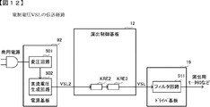
図12は、電源電圧VSLの伝送経路を示している。電源基板92では、変圧回路501、直流電圧生成回路502などを用いて、外部電源である商用電源から直流34Vの電源電圧VSL2が生成される。例えば変圧回路501では、交流24Vの電源電圧が生成される。直流電圧生成回路502は、整流回路や平滑回路を含み、交流24Vの電源電圧を整流、平滑して直流34Vの電源電圧VSL2を生成する。直流34Vの電源電圧VSL2は、フィードバック制御などによる電圧制御が行われていないので、交流24Vの電源電圧の変動により、直流34Vの電源電圧VSL2も変動する。このように、レセプタクルKRE2の端子TA13、TA14に供給される直流34Vの電源電圧VSL2は、電圧制御が行われていない変動幅(リップル成分)が大きい直流電圧である。これに対し、レセプタクルKRE2の端子TA15〜TA20に供給される直流12Vの電源電圧VDD2、レセプタクルKRE2の端子TA21〜TA24に供給される直流5Vの電源電圧VCC2、レセプタクルKRE2の端子TA27、TA28に供給される直流12Vの電源電圧VDD3は、いずれも電源基板92において、フィードバック制御による電圧制御が行われ、直流34Vの電源電圧VSLと比較して、変動幅(リップル成分)が少ない直流電圧であればよい。
FIG. 12 shows a transmission path of the power supply voltage VSL. In the
演出制御基板12において、直流34Vの電源電圧VSLに対応する電源ラインLSLにはフィルタ回路などの電圧を安定化する安定化回路が介在しない。その一方で、ドライバ基板19では、直流34Vの電源電圧VSLをフィルタ回路511に入力して、電圧を安定化する。また、演出制御基板12において、直流34Vの電源電圧VSLとは異なる電源電圧に対応する電源ラインにはフィルタ回路などにより電圧を安定化する安定化回路が介在する。
In the
例えば電源基板配線用のレセプタクルKRE2において、直流12Vの電源電圧VDD2が供給される端子TA15〜TA20は、フィルタ回路131aに接続され、直流5Vの電源電圧VCC2が供給される端子TA21〜TA24は、フィルタ回路131bに接続され、直流12Vの電源電圧VDD3が供給される端子TA27、TA28は、フィルタ回路131cに接続されている。フィルタ回路131aの出力部は直流12Vの電源電圧VDSを供給する電源ラインLDSに接続され、フィルタ回路131bの出力部は直流5Vの電源電圧VCCを供給する電源ラインLCCに接続され、フィルタ回路131cの出力部は直流12Vの電源電圧VDCを供給する電源ラインLDCに接続されている。こうして、フィルタ回路131aはレセプタクルKRE2の端子TA15〜TA20と直流12Vの電源電圧VDSに対応する電源ラインLDSとの間に介在し、フィルタ回路131bはレセプタクルKRE2の端子TA21〜TA24と直流5Vの電源電圧VCCに対応する電源ラインLCCとの間に介在し、フィルタ回路131cはレセプタクルKRE2の端子TA27、TA28と直流12Vの電源電圧VDCに対応する電源ラインLDCとの間に介在する。
For example, in the receptacle KRE2 for power supply substrate wiring, the terminals TA15 to TA20 to which the DC 12V power supply voltage VDD2 is supplied are connected to the
電源ラインLSLは、直流34Vの電源電圧VSLを供給するために設けられている。電源ラインLDSは、直流12Vの電源電圧VDSを供給するために設けられている。電源ラインLCCは、直流5Vの電源電圧VCCを供給するために設けられている。電源ラインLDCは、直流12Vの電源電圧VDCを供給するために設けられている。したがって、フィルタ回路が介在しない電源ラインLSLは、フィルタ回路が介在する電源ラインLDS、LCC、LDCのいずれと比較しても、高い電源電圧を供給するために設けられている。 The power supply line LSL is provided to supply a power supply voltage VSL of DC 34V. The power supply line LDS is provided to supply a power supply voltage VDS of DC 12V. The power supply line LCC is provided for supplying a power supply voltage VCC of DC 5V. The power supply line LDC is provided for supplying a power supply voltage VDC of 12V DC. Therefore, the power supply line LSL without the filter circuit is provided to supply a higher power supply voltage than any of the power supply lines LDS, LCC, and LDC with the filter circuit interposed.
レセプタクルKRE2では、直流12Vの電源電圧VDD2が供給される6つの端子TA15〜TA20、直流5Vの電源電圧VCC2が供給される4つの端子TA21〜TA24、直流12Vの電源電圧VDD3が供給される2つの端子TA27、TA28が設けられる一方で、直流34Vの電源電圧VSL2が供給される2つの端子TA13、TA14が設けられる。そのため、レセプタクルKRE2では、電源電圧が供給される端子のうちで、フィルタ回路に接続された端子TA15〜TA20、TA21〜TA24、TA27、TA28の端子数が、フィルタ回路に接続されていない端子TA13、TA14の端子数よりも多くなる。なお、それぞれの電源電圧に対応した端子数は、電源容量や負荷電流に応じて設定したものであればよい。 In the receptacle KRE2, six terminals TA15 to TA20 to which a DC 12V power supply voltage VDD2 is supplied, four terminals TA21 to TA24 to which a DC 5V power supply voltage VCC2 is supplied, and two terminals to which a DC 12V power supply voltage VDD3 is supplied. While terminals TA27 and TA28 are provided, two terminals TA13 and TA14 to which a power supply voltage VSL2 of DC 34V is supplied are provided. Therefore, in the receptacle KRE2, among the terminals to which the power supply voltage is supplied, the number of terminals TA15 to TA20, TA21 to TA24, TA27, and TA28 connected to the filter circuit is equal to the terminal TA13 that is not connected to the filter circuit. More than the number of terminals of TA14. The number of terminals corresponding to each power supply voltage may be set according to the power supply capacity and load current.
レセプタクルKRE2では、端子TA15〜TA20に直流12Vの電源電圧VDD2が供給され、端子TA21〜TA24に直流5Vの電源電圧VCC2が供給され、端子TA27、TA28に直流12Vの電源電圧VDD3が供給される一方で、端子TA13、TA14に直流34Vの電源電圧VSL2が供給される。そして、レセプタクルKRE2の端子TA15〜TA20と直流12Vの電源電圧VDSを供給する電源ラインLDSとの間にはフィルタ回路131aが介在し、レセプタクルKRE2の端子TA21〜TA24と直流5Vの電源電圧VCCを供給する電源ラインLCCとの間にはフィルタ回路131bが介在し、レセプタクルKRE2の端子TA27、TA28と直流12Vの電源電圧VDCを供給する電源ラインLDCとの間にはフィルタ回路131cが介在する。これに対し、レセプタクルKRE2の端子TA13、TA14と直流34Vの電源電圧VSLを供給する電源ラインLSLとの間にはフィルタ回路が介在しない。このように、フィルタ回路が介在する電源ラインLDS、LCC、LDCは、直流12Vあるいは直流5Vといった複数種類の電源電圧を供給可能であり、フィルタ回路が介在しない電源ラインLSLは、直流34Vという一種類の電源電圧を供給可能である。レセプタクルKRE2では、端子TA13、TA14が端子TA15〜TA24などよりも外側に配置されている。あるいは、レセプタクルKRE2では、端子TA15〜TA24、TA27、TA28のうちで、例えば端子TA15〜TA24のように、端子TA13、TA14よりも内側に配置された端子が含まれている。
In the receptacle KRE2, a 12V DC power supply voltage VDD2 is supplied to the terminals TA15 to TA20, a 5V DC power supply voltage VCC2 is supplied to the terminals TA21 to TA24, and a 12V DC power supply voltage VDD3 is supplied to the terminals TA27 and TA28. Thus, the power supply voltage VSL2 of DC 34V is supplied to the terminals TA13 and TA14. A
レセプタクルKRE2では、端子TA11、TA12と、端子TA29、TA30との間に、端子TA13〜TA24、TA27、TA28が配置される。端子TA13〜TA24、TA27、TA28は、いずれも電源電圧が供給される端子であり、各種の電源電圧に接続される電源電圧端子となる。これに対し、端子TA11、TA12と、端子TA29、TA30とは、いずれも電源電圧が供給されない端子であり、接地電圧に接続される接地端子となる。したがって、レセプタクルKRE2では、接地端子となる端子TA11、TA12と端子TA29、TA30との間に、電源電圧端子となる端子TA13〜TA24、TA27、TA28が配置される。 In the receptacle KRE2, terminals TA13 to TA24, TA27, and TA28 are arranged between the terminals TA11 and TA12 and the terminals TA29 and TA30. Terminals TA13 to TA24, TA27, and TA28 are all terminals to which a power supply voltage is supplied, and serve as power supply voltage terminals connected to various power supply voltages. On the other hand, the terminals TA11 and TA12 and the terminals TA29 and TA30 are terminals to which no power supply voltage is supplied, and are ground terminals connected to the ground voltage. Therefore, in the receptacle KRE2, terminals TA13 to TA24, TA27, and TA28 that are power supply voltage terminals are arranged between the terminals TA11 and TA12 that are ground terminals and the terminals TA29 and TA30.
レセプタクルKRE2では、端子TA11、TA12と、端子TA25、TA26との間に、端子TA13、TA14と、端子TA15〜TA24とが配置され、端子TA25、TA26と、端子TA29、TA30との間に、端子TA27、TA28が配置される。端子TA13、TA14は、直流34Vの電源電圧VSL2が供給される端子であり、電源電圧VSL2に接続される電源電圧端子である。端子TA15〜TA20は、直流12Vの電源電圧VDD2が供給される端子であり、電源電圧VDD2に接続される電源電圧端子である。端子TA21〜TA24は、直流5Vの電源電圧VCC2が供給される端子であり、電源電圧VCC2に接続される電源電圧端子である。端子TA27、TA28は、直流12Vの電源電圧VDD3が供給される端子であり、電源電圧VDD3に接続される電源電圧端子である。そのため、直流34Vの電源電圧VSL2に接続される電源電圧端子としての端子TA13、TA14と、直流34Vの電源電圧VSL2以外の電源電圧に接続される電源電圧端子としての端子TA15〜TA24、TA27、TA28のうちの一部である端子TA15〜TA24とが、接地端子となる端子TA11、TA12と端子TA25、TA26との間に配置される。また、直流34Vの電源電圧VSL2以外の電源電圧に接続される電源電圧端子としての端子TA15〜TA24、TA27、TA28のうちで、他の一部である端子TA27、TA28が、接地端子となる端子TA25、TA26と端子TA29、TA30との間に配置される。 In the receptacle KRE2, the terminals TA13 and TA14 and the terminals TA15 to TA24 are arranged between the terminals TA11 and TA12 and the terminals TA25 and TA26, and the terminals TA25 and TA26 are connected between the terminals TA29 and TA30. TA27 and TA28 are arranged. Terminals TA13 and TA14 are terminals to which a power supply voltage VSL2 of DC 34V is supplied, and are power supply voltage terminals connected to the power supply voltage VSL2. Terminals TA15 to TA20 are terminals to which a 12V DC power supply voltage VDD2 is supplied and are connected to the power supply voltage VDD2. Terminals TA21 to TA24 are terminals to which a power supply voltage VCC2 of DC 5V is supplied, and are power supply voltage terminals connected to the power supply voltage VCC2. Terminals TA27 and TA28 are terminals to which a DC power supply voltage VDD3 of 12V is supplied, and are power supply voltage terminals connected to the power supply voltage VDD3. Therefore, terminals TA13 and TA14 as power supply voltage terminals connected to the power supply voltage VSL2 of DC 34V, and terminals TA15 to TA24, TA27 and TA28 as power supply voltage terminals connected to power supply voltages other than the power supply voltage VSL2 of DC 34V. The terminals TA15 to TA24, which are part of the terminals TA15 and TA24, are arranged between the terminals TA11 and TA12 serving as ground terminals and the terminals TA25 and TA26. Among the terminals TA15 to TA24, TA27, and TA28 as power supply voltage terminals connected to a power supply voltage other than the DC 34V power supply voltage VSL2, the other terminals TA27 and TA28 serve as ground terminals. Arranged between TA25, TA26 and terminals TA29, TA30.
端子TA27、TA28に供給される直流12Vの電源電圧VDD3は、降圧コンバータ回路132により直流1.05Vの電源電圧を生成するために用いられる。直流1.05Vの電源電圧は、例えば表示制御部123のグラフィックスプロセッサといった、特定のマイクロプロセッサに供給される。したがって、レセプタクルKRE2では、電源電圧に接続される端子TA13〜TA24、TA27、TA28のうちで、変動幅(リップル成分)が比較的に大きい直流34Vの電源電圧VSL2に接続される端子TA13、TA14は、表示制御部123のグラフィックスプロセッサといった特定のマイクロプロセッサに供給する電源電圧の生成に用いられる直流12Vの電源電圧VDD3に接続されるTA27、TA28から最も離れて配置される。
The DC 12V power supply voltage VDD3 supplied to the terminals TA27 and TA28 is used by the step-down
演出制御基板12では、直流34Vの電源電圧VSL2を安定化してから電源電圧VSLとして出力する場合も考えられる。しかしながら、演出制御基板12では直接的な用途のない直流34Vの電源電圧VSL2を安定化する回路素子の設置は、部品点数や基板容積の増大を招き、電力損失や製造コストも増加する。また、特別な回路素子の設置により、演出制御基板12のリユースや共通化が困難になるおそれもある。そこで、電圧制御が行われていない直流34Vの電源電圧VSL2は、そのまま電源電圧VSLとして演出制御基板12から出力され、ドライバ基板19にてフィルタ回路511に入力して電圧を安定化する。これにより、部品点数や基板容積の増大、電力損失や製造コストの増加を防止する適切な基板構成が可能になる。また、演出制御基板12のリユースや共通化が容易に行われる適切な基板構成が可能になる。また、電源ラインLSLは、演出制御基板12における主要な電気回路や電気部品から離れて配置されることにより、変動幅(リップル成分)が大きい直流電圧によるノイズの悪影響を防止する適切な基板構成が可能になる。
In the
演出制御基板12において、直流34Vの電源電圧VSLを供給する電源ラインLSLは、直流12Vの電源電圧VDSを供給する電源ラインLDS、直流5Vの電源電圧VCCを供給する電源ラインLCC、直流12Vの電源電圧VDSを供給する電源ラインLDSのいずれと比較しても、高い電源電圧となる直流34Vを供給する。一般的に、高い電源電圧を安定化する安定化回路は、低い電源電圧を安定化する安定化回路よりも、回路素子の容積や電力損失が大きなものになりやすく、回路素子の値段が高価なものになりやすい。そこで、高い電源電圧となる直流34Vの電源電圧VSLを供給する電源ラインLSLにはフィルタ回路が介在しないことにより、基板容積の増大、電力損失や製造コストの増加を防止する適切な基板構成が可能になる。
In the
レセプタクルKRE2において、2つの端子TA13、TA14には直流34Vの電源電圧VSLが供給される。これに対し、レセプタクルKRE2において、6つの端子TA15〜TA20には直流12Vの電源電圧VDD2が供給され、4つの端子TA21〜TA24には直流5Vの電源電圧VCC2が供給され、2つの端子TA27、TA28には直流12Vの電源電圧VDD3が供給される。したがって、演出制御基板12では、レセプタクルKRE2にて電源電圧が供給される端子のうちで、フィルタ回路131a〜131cのいずれかに接続される端子TA15〜TA24、TA27、TA28の端子数が、フィルタ回路に接続されない端子TA13、TA14の端子数よりも多くなる。このように端子数が設定されているので、例えば演出制御基板12にて電圧を安定化する対象となる電源電圧の用途や電源容量などに応じて、配線設計の自由度を向上させる適切な基板構成が可能になる。
In the receptacle KRE2, a power supply voltage VSL of DC 34V is supplied to the two terminals TA13 and TA14. In contrast, in the receptacle KRE2, a DC 12V power supply voltage VDD2 is supplied to the six terminals TA15 to TA20, and a DC 5V power supply voltage VCC2 is supplied to the four terminals TA21 to TA24. Is supplied with a power supply voltage VDD3 of DC 12V. Therefore, in the
レセプタクルKRE2において、電源電圧が供給される端子のうちで、演出制御基板12にてフィルタ回路131a〜131cのいずれかに接続される端子TA15〜TA24、TA27、TA28は、直流12Vの電源電圧VDD2を供給可能な端子TA15〜TA20と、直流5Vの電源電圧VCC2を供給可能な端子TA21〜TA24と、直流12Vの電源電圧VDD3を供給可能な端子TA27、TA28とを、含んでいる。これに対し、レセプタクルKRE2において、電源電圧が供給される端子のうちで、演出制御基板12ではフィルタ回路に接続されない端子TA13、TA14は、直流34Vの電源電圧VSL2を供給可能であり、他の種類の電源電圧は供給しない。そのため、フィルタ回路が介在する電源ラインであるか、フィルタ回路が介在しない電源ラインであるかに応じて、供給可能な電源電圧の種類数が異なっている。より具体的には、フィルタ回路が介在する電源ラインは、直流12Vの電源電圧VDD2、直流5Vの電源電圧VCC2、直流12Vの電源電圧VDD2といった、複数種類の電源電圧を供給可能であり、フィルタ回路が介在しない電源ラインは、直流34Vの電源電圧VSLという一種類の電源電圧を供給可能である。このように、電源ラインに対応して供給可能な電源電圧の種類数が異なるので、例えば演出制御基板12にて電圧を安定化する対象となる電源電圧の用途などに応じて、配線設計の自由度を向上させる適切な基板構成が可能になる。
In the receptacle KRE2, among the terminals to which the power supply voltage is supplied, the terminals TA15 to TA24, TA27, and TA28 connected to any one of the
また、フィルタ回路が介在しない電源ラインに接続された端子TA13、TA14は、フィルタ回路が介在する電源ラインに接続された端子TA15〜TA24などよりも外側に配置されている。このような端子の配置により、例えば演出制御基板12にて電圧を安定化する対象となる電源電圧の用途などに応じて、配線設計の自由度を向上させる適切な基板構成が可能になる。加えて、端子TA13、TA14に供給された直流34Vの電源電圧VSL2を、そのまま電源電圧VSLとしてドライバ基板19に対して出力するための配線長を短縮する適切な基板構成が可能になる。
The terminals TA13 and TA14 connected to the power supply line not including the filter circuit are disposed outside the terminals TA15 to TA24 connected to the power supply line including the filter circuit. Such an arrangement of terminals enables an appropriate board configuration that improves the degree of freedom in wiring design according to, for example, the use of a power supply voltage for which the voltage is to be stabilized by the
レセプタクルKRE2において、端子TA13〜TA24、TA27、TA28は、各種の電源電圧に接続される電源電圧端子となる。これに対し、レセプタクルKRE2において、端子TA11、TA12と、端子TA29、TA30とは、いずれも接地電圧に接続される接地端子となる。そして、端子TA13〜TA24、TA27、TA28は、端子TA11、TA12と、端子TA29、TA30との間に配置されている。このような端子の配置により、ノイズの影響を受けにくい適切な基板構成が可能になる。また、電源電圧を遮蔽して、ノイズの発生を防止する適切な基板構成が可能になる。 In the receptacle KRE2, the terminals TA13 to TA24, TA27, and TA28 are power supply voltage terminals connected to various power supply voltages. On the other hand, in the receptacle KRE2, the terminals TA11 and TA12 and the terminals TA29 and TA30 are all ground terminals connected to the ground voltage. The terminals TA13 to TA24, TA27, and TA28 are disposed between the terminals TA11 and TA12 and the terminals TA29 and TA30. Such an arrangement of terminals enables an appropriate substrate configuration that is less susceptible to noise. In addition, an appropriate substrate configuration that shields the power supply voltage and prevents the generation of noise can be realized.
レセプタクルKRE2において、端子TA15〜TA24、TA27、TA28は、直流34Vの電源電圧VSL2とは異なる電源電圧に接続される第1電源電圧端子となる。その一方で、レセプタクルKRE2において、端子TA13、TA14は、直流34Vの電源電圧VSL2に接続される第2電源電圧端子となる。また、レセプタクルKRE2において、端子TA11、TA12は接地電圧に接続される第1接地端子となり、端子TA25、TA26は接地電圧に接続される第2接地端子となり、端子TA29、TA30は接地電圧に接続される第3接地端子となる。そして、レセプタクルKRE2では、第2電源電圧端子に含まれる端子TA13、TA14と、第1電源電圧端子に含まれる端子TA15〜TA24とが、第1接地端子に含まれる端子TA11、TA12と、第2接地端子に含まれる端子TA25、TA26との間に配置され、第1電源電圧端子に含まれる端子TA27、TA28が、第2接地端子に含まれる端子TA25、TA26と、第3接地端子に含まれる端子TA29、TA30との間に配置される。このような端子の配置により、ノイズの影響を受けにくい適切な基板構成が可能になる。特に、第2接地端子に含まれる端子TA25、TA26を、第2電源電圧端子に含まれる端子TA13、TA14および第1電源電圧端子に含まれる端子TA15〜TA24と、第1電源電圧端子に含まれるTA27、TA28との間に配置させることで、さらにノイズの影響を受けにくい適切な基板構成が可能になる。また、電源電圧を効率よく遮蔽して、さらにノイズの発生を防止する適切な基板構成が可能になる。加えて、直流34Vの電源電圧VSL2に接続される端子TA13、TA14は、表示制御部123のグラフィックスプロセッサといった特定のマイクロプロセッサに供給する電源電圧の生成に用いられる直流12Vの電源電圧VDD3に接続されるTA27、TA28から離れて配置されるので、特定のマイクロプロセッサがノイズの影響を受けにくい適切な基板構成が可能になる。
In the receptacle KRE2, the terminals TA15 to TA24, TA27, and TA28 are first power supply voltage terminals that are connected to a power supply voltage different from the DC power supply voltage VSL2. On the other hand, in the receptacle KRE2, the terminals TA13 and TA14 become second power supply voltage terminals connected to the power supply voltage VSL2 of DC 34V. In the receptacle KRE2, the terminals TA11 and TA12 are first ground terminals connected to the ground voltage, the terminals TA25 and TA26 are second ground terminals connected to the ground voltage, and the terminals TA29 and TA30 are connected to the ground voltage. A third ground terminal. In the receptacle KRE2, the terminals TA13 and TA14 included in the second power supply voltage terminal, the terminals TA15 to TA24 included in the first power supply voltage terminal, the terminals TA11 and TA12 included in the first ground terminal, and the second The terminals TA27 and TA28 which are disposed between the terminals TA25 and TA26 included in the ground terminal and are included in the first power supply voltage terminal are included in the terminals TA25 and TA26 included in the second ground terminal and the third ground terminal. Arranged between terminals TA29 and TA30. Such an arrangement of terminals enables an appropriate substrate configuration that is less susceptible to noise. In particular, the terminals TA25 and TA26 included in the second ground terminal are included in the terminals TA13 and TA14 included in the second power supply voltage terminal and the terminals TA15 to TA24 included in the first power supply voltage terminal and the first power supply voltage terminal. By disposing them between TA27 and TA28, an appropriate substrate configuration that is less susceptible to noise becomes possible. In addition, an appropriate substrate configuration that efficiently shields the power supply voltage and prevents the generation of noise can be realized. In addition, the terminals TA13 and TA14 connected to the DC 34V power supply voltage VSL2 are connected to the DC 12V power supply voltage VDD3 used to generate a power supply voltage to be supplied to a specific microprocessor such as a graphics processor of the
演出制御基板12では、レセプタクルKRE2の端子TA15〜TA20にて供給された電源電圧VDD2から、分岐点DB1にて電源電圧VDLが分岐される。このような分岐点DB1にて電源電圧VDLが分岐された後に、フィルタ回路131aにより電源電圧VDSを安定化する。電源電圧VDLは、例えば演出用LED61に含まれる特定のLEDといった、特定の電気部品を駆動するために用いられる直流12Vの電源電圧である。電源電圧VDSは、増幅回路521に供給され、音声信号を出力するために用いられる直流12Vの電源電圧である。このように、フィルタ回路131aは、1の電源電圧VDD2を、電源電圧VDLと電源電圧VDSとに分岐した後に、電源電圧VDSを安定化する。演出制御基板12には、増幅回路521が設けられ、スピーカ8L、8Rに供給される音声信号を出力可能としてもよい。
In the
図13(A)は、電源電圧VDSを供給するための配線における配線長の関係を示している。演出制御基板12において、電源電圧VDSを増幅回路521に供給するための電源ラインLDSは、分岐点DB1からフィルタ回路131aの入力部までの配線長LL1を有する配線と、フィルタ回路131aの出力部から増幅回路521の入力部までの配線長LL2を有する配線とを、含んでいればよい。そして、配線長LL2は、配線長LL1よりも短くなるように、演出制御基板12における配線や回路の配置が調整されていればよい。このように、フィルタ回路131aから増幅回路521までの配線長LL2は、電源電圧VDSを分岐点DB1にて分岐させてからフィルタ回路131aまでの配線長LL1よりも短くなる。なお、増幅回路521やフィルタ回路131aは、演出制御基板12に設置されるものに限定されず、音声制御基板13に設置されてもよい。
FIG. 13A shows the relationship between the wiring lengths of the wirings for supplying the power supply voltage VDS. In the
図13(B)は、増幅回路521やフィルタ回路131aを音声制御基板13に設置した場合における電源電圧VDSの伝送経路を示している。電源基板92では、変圧回路501、直流電圧生成回路502などを用いて、外部電源である商用電源から直流12Vの電源電圧VDD2が生成される。直流12Vの電源電圧VDD2は、電源基板配線用のレセプタクルKRE2において、端子TA15〜TA20に供給される。演出制御基板12では、レセプタクルKRE2の端子TA15〜TA20にて供給された電源電圧VDD2から、分岐点DB1にて電源電圧VDLが分岐された後、そのまま電源電圧VDSとして演出制御基板12から出力され、音声基板配線用のレセプタクルKRE4に接続された音声制御基板配線を経由して、音声制御基板13に供給されてもよい。例えば、電源基板配線用のレセプタクルKRE2において、電源電圧VDD2の供給を受ける端子TA15〜TA20は、電源ラインLDSに接続され、電源ラインLDSが音声制御基板配線用のレセプタクルKRE4における所定端子に接続されていればよい。演出制御基板12において、直流12Vの電源電圧VDSに対応する電源ラインLDSにはフィルタ回路などの電圧を安定化する安定化回路が介在しなくてもよい。その一方で、音声制御基板13では、直流12Vの電源電圧VDSをフィルタ回路131aに入力して、電圧を安定化する。こうして安定化された電源電圧VDSを増幅回路521に供給すればよい。
FIG. 13B shows a transmission path of the power supply voltage VDS when the
音声制御基板13には、音声制御用IC522、音声データROM523などが設けられてもよい。音声制御用IC522は、演出制御基板12の演出制御用CPU120などから出力された指令(音番号データなど)に応じて、音声や効果音を生成するための信号処理を実行する。音声データROM523は、音番号データに応じた制御データを記憶している。音番号データに応じた制御データは、所定期間(例えば飾り図柄の可変表示期間)における音声や効果音の出力態様を時系列的に示すデータの集まりである。なお、音声制御基板13に設けられる各種の構成を、演出制御基板12に設けられるように構成し、音声制御基板13を備えないものであってもよい。
The
音声制御用IC522などにより生成された音声信号を増幅して、スピーカ8L、8Rなどに出力可能な増幅回路521は、電源電圧に変動が生じると、出力される音声信号に歪みが生じるといった、音質に悪影響が及ぶおそれがある。そこで、直流12Vの電源電圧VDSは、フィルタ回路131aにより安定化した後に、増幅回路521に供給される。演出制御基板12において、1の電源電圧VDD2を、特定の電気部品を駆動するための電源電圧VDLと、増幅回路521に供給するための電源電圧VDSとに分岐した後に、フィルタ回路131aを用いて安定化した電源電圧VDSを増幅回路521に供給する。このように、フィルタ回路131aを用いて安定化した電源電圧VDSを増幅回路521に供給することで、増幅回路521を安定して動作させる適切な基板構成が可能になる。
The
増幅回路521に供給するための電源電圧VDSに対応する電源ラインLDSにおいて、フィルタ回路131aから増幅回路521までの配線長LL2は、分岐点DB1にて電源電圧VDLが分岐されてからフィルタ回路131aに入力するまでの配線長LL1よりも短くなる。このように、フィルタ回路131aを用いて安定化した電源電圧VDSを増幅回路521に供給するまでの配線長を短くすることで、ノイズの影響を受けにくく、増幅回路521を安定して動作させる適切な基板構成が可能になる。
In the power supply line LDS corresponding to the power supply voltage VDS supplied to the
演出制御基板12では、レセプタクルKRE2の端子TA21〜TA24にて供給された電源電圧VCC2から、電源電圧VCLが分岐される。電源電圧VCLが分岐された後に、フィルタ回路131bにより電源電圧VCCを安定化する。電源電圧VCLは、例えば演出用モータ60に含まれる特定のモータや演出用LED61に含まれる特定のLEDといった、特定の電気部品を駆動するために用いられる直流5Vの電源電圧である。電源電圧VCCは、例えば演出制御用CPU120といった、所定の電気回路を駆動するために用いられる直流5Vの直流電源である。このように、フィルタ回路131bは、1の電源電圧VCC2を、電源電圧VCLと電源電圧VDDとに分岐した後の電源電圧VDDを安定化する。
In the
演出制御基板12では、レセプタクルKRE2の端子TA27、TA28にて供給された電源電圧VDD3を、フィルタ回路131cにより安定化した後に、電源電圧VDCを供給可能に分岐させる。電源電圧VDCは、電源断の発生を監視するために用いられる直流12Vの電源電圧である。また、電源電圧VDD3は、フィルタ回路131cにより安定化した後に、降圧コンバータ回路132に入力される。降圧コンバータ回路132は、1入力2出力の直流電圧を変換する回路である。図11に示す降圧コンバータ回路132は、直流12Vの電源電圧VDD3をフィルタ回路131cにより安定化した電圧が入力されて、直流1.05Vの電源電圧と、直流3.3Vの電源電圧とに変換して出力する。降圧コンバータ回路132の出力部は、直流1.05Vの電源電圧を供給する電源ラインL10と、直流3.3Vの電源電圧を供給する電源ラインL33とに接続されている。直流1.05Vの電源電圧は、例えば表示制御部123に含まれるグラフィックスプロセッサといった、所定の電気回路を駆動するために用いられる。直流3.3Vの電源電圧は、例えばROM121や表示制御部123に含まれる画像データメモリといった、所定の電気回路を駆動するために用いられる。直流3.3Vの電源電圧は、レギュレータ回路133にも入力される。レギュレータ回路133は、例えばLDO(Low Drop-Out)レギュレータなどのシリーズレギュレータといったリニア方式の安定化電源回路であればよく、直流3.3Vの電源電圧が入力されて、直流1.5Vの電源電圧に変換して出力する。レギュレータ回路133の出力部は、直流1.5Vの電源電圧を供給する電源ラインL15に接続されている。直流1.5Vの電源電圧は、例えばRAM122といった、所定の電気回路を駆動するために用いられる。
In the
図14は、フィルタ回路131a〜131cの構成例を示している。図14(A)は、電源電圧VDSに対応するフィルタ回路131aの構成例を示している。図14(B)は、電源電圧VCCに対応するフィルタ回路131bの構成例を示している。図14(C)は、電源電圧VDCに対応するフィルタ回路131cの構成例を示している。
FIG. 14 shows a configuration example of the
図14(A)に示すフィルタ回路131aは、三端子コンデンサ85a、バイパスコンデンサC10、C11、電解コンデンサC1を用いて構成されていればよい。バイパスコンデンサC10、C11は、電解コンデンサC1と比較して、高周波のノイズを防止するノイズ対策用の電気部品であり、デカップリングコンデンサともいう。電解コンデンサC1は、バイパスコンデンサC10、C11と比較して、低周波のノイズを防止するノイズ対策用の電気部品である。三端子コンデンサ85aの入力端子(IN)は、フィルタ回路131aの入力部となり、直流12Vの電源電圧VDD2が供給される。三端子コンデンサ85aの出力端子(OUT)は、フィルタ回路131aの出力部となり、電圧が安定化された直流12Vの電源電圧VDSを供給する。三端子コンデンサ85aの接地端子(GND)は、接地(グランドラインに接続)されている。三端子コンデンサ85aの出力端子と接地端子との間には、0.1μFのバイパスコンデンサC10、47μFのバイパスコンデンサC11、1000μFの電解コンデンサC1が、接続されている。
The
図14(B)に示すフィルタ回路131bは、三端子コンデンサ85b、バイパスコンデンサC12、C13、電解コンデンサC2を用いて構成されていればよい。バイパスコンデンサC12、C13は、電解コンデンサC2と比較して、高周波のノイズを防止するノイズ対策用の電気部品である。電解コンデンサC2は、バイパスコンデンサC12、C13と比較して、低周波のノイズを防止するノイズ対策用の電気部品である。三端子コンデンサ85bの入力端子(IN)は、フィルタ回路131bの入力部となり、直流5Vの電源電圧VCC2が供給される。三端子コンデンサ85bの出力端子(OUT)は、フィルタ回路131bの出力部となり、電圧が安定化された直流5Vの電源電圧VCCを供給する。三端子コンデンサ85bの接地端子(GND)は、接地(グランドラインに接続)されている。三端子コンデンサ85bの出力端子と接地端子との間には、0.1μFのバイパスコンデンサC12、47μFのバイパスコンデンサC13、1000μFの電解コンデンサC2が、接続されている。
The
図14(C)に示すフィルタ回路131cは、三端子コンデンサ85c、バイパスコンデンサC14、電解コンデンサC3を用いて構成されていればよい。バイパスコンデンサC14は、電解コンデンサC3と比較して、高周波のノイズを防止するノイズ対策用の電気部品である。電解コンデンサC3は、バイパスコンデンサC14と比較して、低周波のノイズを防止するノイズ対策用の電気部品である。三端子コンデンサ85cの入力端子(IN)は、フィルタ回路131cの入力部となり、直流12Vの電源電圧VDD3が供給される。三端子コンデンサ85cの出力端子(OUT)は、フィルタ回路131cの出力部となり、電圧が安定化された直流12Vの電源電圧VDCを供給する。三端子コンデンサ85cの接地端子(GND)は、接地(グランドラインに接続)されている。三端子コンデンサ85cの出力端子と接地端子との間には、0.1μFのバイパスコンデンサC14、1000μFの電解コンデンサC3が、接続されている。
The
フィルタ回路131a〜131cは、各電源経路の電圧を安定化する安定化回路として機能する。例えばフィルタ回路131aは、電源ラインLDSにより供給される直流12Vの電源電圧VDSを安定化する。フィルタ回路131bは、電源ラインLCCにより供給される直流5Vの電源電圧VCCを安定化する。フィルタ回路131cは、電源ラインLDCにより供給される直流12Vの電源電圧を安定化する。演出制御基板12には、フィルタ回路131a〜131cの他にも、各種電源電圧におけるノイズの発生を防止するノイズ防止回路が設けられてもよい。
The
図15は、演出制御基板12に設けられるノイズ防止回路の構成例を示している。図15(A)は、電源電圧VDLというLED用DC12V(直流12V)に対応するノイズ防止回路135aの構成例を示している。図15(B)は、電源電圧VCLというLED/モータ用DC5V(直流5V)に対応するノイズ防止回路135bの構成例を示している。図15(C)は、電源電圧VCCというIC用DC5V(直流5V)や直流3.3Vの電源電圧というIC用DC3.3V(直流3.3V)に対応するノイズ防止回路135cの構成例を示している。
FIG. 15 shows a configuration example of a noise prevention circuit provided on the
図15(A)に示すノイズ防止回路135aは、直列接続されたコンデンサC20および抵抗R20と、直列接続されたコンデンサC21および抵抗R21と、直列接続されたコンデンサC22および抵抗R22とを用いて構成されていればよい。これらの構成は、いずれも電源電圧VDLを供給する電源ラインLDLと接地電圧を提供する接地端子(グランドライン)とに接続されていればよい。コンデンサC20、C21、C22は、いずれも0.1μFのバイパスコンデンサであればよい。抵抗R20、R21、R22は、いずれも22Ωの抵抗値を有するものであればよい。
A
図15(B)に示すノイズ防止回路135bは、直列接続されたコンデンサC23および抵抗R23と、直列接続されたコンデンサC24および抵抗R24とを用いて構成されていればよい。これらの構成は、いずれも電源電圧VCLを供給する電源ラインLCLと接地電圧を提供する接地端子(グランドライン)とに接続されていればよい。コンデンサC23、C24は、いずれも0.1μFのバイパスコンデンサであればよい。抵抗R23、R24は、いずれも22Ωの抵抗値を有するものであればよい。
The
図15(C)に示すノイズ防止回路135cは、コンデンサC25〜C28を用いて構成されていればよい。コンデンサC25は、電源電圧VCCを供給する電源ラインLCCと接地電圧を提供する接地端子(グランドライン)とに接続されていればよい。コンデンサC26、C27、C28は、いずれも直流3.3Vの電源電圧を供給する電源ラインL33と接地電圧を提供する接地端子(グランドライン)とに接続されていればよい。コンデンサC25〜C28は、いずれも0.1μFのバイパスコンデンサであればよい。
The
図15(A)に示すノイズ防止回路135aでは、コンデンサC20、C21、C22に加え、抵抗R20、R21、R22が用いられている。図15(B)に示すノイズ防止回路135bでは、コンデンサC23、C24に加え、抵抗R23、R24が用いられている。その一方で、図15(C)に示すノイズ防止回路135cでは、コンデンサC25〜C28が用いられ、抵抗は用いられていない。このように、ノイズ防止回路135a、135bでは、ノイズ防止回路135cとは異なる回路素子として、抵抗R20、R21、R22や、抵抗R23、R24が、用いられている。
In the
図15(A)に示すノイズ防止回路135aにより安定化される電源電圧VDLは、例えば演出用LED61に含まれる特定のLEDといった、特定の電気部品を駆動するために用いられる。電源ラインLDLは、例えば演出用LED61に含まれる特定のLEDといった、特定の電気部品を駆動するための電源電圧VDLを供給する。図15(B)に示すノイズ防止回路135bにより安定化される電源電圧VCLは、例えば演出用モータ60に含まれる特定のモータや演出用LED61に含まれる特定のLEDといった、特定の電気部品を駆動するために用いられる。電源ラインLCLは、例えば演出用モータ60に含まれる特定のモータや演出用LED61に含まれる特定のLEDといった、特定の電気部品を駆動するための電源電圧VCLを供給する。図15(C)に示すノイズ防止回路135cにより安定化される電源電圧VCCと直流3.3Vの電源電圧は、例えば演出制御用CPU120やROM121あるいは表示制御部123に含まれる画像データメモリといった、特定の制御回路を含む電気回路を駆動するために用いられる。電源ラインLCCは、例えば演出制御用CPU120といった、特定の制御回路を含む電気回路を駆動するための電源電圧VCCを供給する。電源ラインL33は、例えばROM121あるいは表示制御部123の画像データメモリといった、特定の制御回路を含む電気回路を駆動するための直流3.3Vの電源電圧を供給する。このように、モータやLEDなど特定の電気部品を駆動するための電源電圧に対応するノイズ防止回路135a、135bでは、CPUやROMなど特定の電気回路を駆動するための電源電圧に対応するノイズ防止回路135cとは異なる回路素子として、抵抗R20、R21、R22や、抵抗R23、R24が、用いられている。
The power supply voltage VDL stabilized by the
演出用モータ60に含まれる特定のモータや演出用LED61に含まれる特定のLEDのような電流駆動型の回路素子を用いた負荷回路では、負荷回路の過渡現象により過大な突入電流が発生して、電気部品が破損してしまうおそれがある。そこで、ノイズ防止回路135aでは、コンデンサC20に抵抗R20を直列接続し、コンデンサC21に抵抗R21を直列接続し、コンデンサC22に抵抗R22を直列接続する。また、ノイズ防止回路135bでは、コンデンサC23に抵抗R23を直列接続し、コンデンサC24に抵抗R24を直列接続する。なお、電源電圧VDLが安定しているときには、コンデンサC20、C21、C22が充電状態となり、抵抗R20、R21、R22は非導通状態となるので、電力損失の発生を防止できる。電源電圧VCLが安定しているときには、コンデンサC23、C24が充電状態となり、抵抗R23、R24は非導通状態となるので、電力損失の発生を防止できる。その一方で、演出制御用CPU120やROM121あるいは表示制御部123の画像データメモリなどの半導体集積回路では、例えばCMOS回路といった、電圧駆動型の回路素子が用いられ、入力インピーダンスが比較的に大きくなる。そのため、回路の過渡現象による突入電流は発生しにくい。そのため、ノイズ防止回路135cでは、コンデンサC25〜C28を用いる一方で、抵抗を用いる必要はない。こうして、電源電圧を供給する対象となる回路や電気部品の特性に応じて異なる回路素子を用いたノイズ防止回路を構成することにより、基板容積の増大や製造コストの増加を防止しつつ、ノイズの発生を防止する適切な基板構成が可能になる。
In a load circuit using a current-driven circuit element such as a specific motor included in the
図16は、電源電圧VDCを用いる電源監視回路140を示している。演出制御基板12では、電源電圧VDCが電源断の発生を監視するために用いられる。電源監視回路140は、例えば停電監視リセットモジュールICを用いて構成され、電源断信号を出力可能な電源監視手段を実現する回路である。例えば電源監視回路140は、電源電圧VDCが所定値(例えば10V)を超えると、オフ状態(ハイレベル)の電源断信号を出力する。その一方で、電源電圧VDCが所定値以下になった期間が、予め定められた待機時間以上継続したときに、オン状態(ローレベル)の電源断信号を出力する。電源監視回路140から出力された電源断信号は、演出制御用CPU120へと伝送される。
FIG. 16 shows a power
電源断信号を出力するための監視対象となる電源電圧VDCは、直流1.05Vの電源電圧や直流3.3Vの電源電圧、直流1.5Vの電源電圧を生成するために用いられる。直流1.05Vの電源電圧は、例えば表示制御部123に含まれるグラフィックスプロセッサといった、所定の電気回路を駆動するために用いられる。直流3.3Vの電源電圧は、例えばROM121や表示制御部123に含まれる画像データメモリといった、所定の電気回路を駆動するために用いられる。直流1.5Vの電源電圧は、例えばRAM122といった、所定の電気回路を駆動するために用いられる。こうした電気回路に供給される電源電圧の生成に用いられる電源電圧VDCを監視対象とすることにより、電気回路の動作状態が不安定となる以前に、電源断信号を出力する(オン状態にする)ことができるので、各種電気回路における誤動作を防止できる。
The power supply voltage VDC to be monitored for outputting the power-off signal is used to generate a power supply voltage of DC 1.05V, a power supply voltage of DC 3.3V, and a power supply voltage of DC 1.5V. The power supply voltage of DC 1.05V is used for driving a predetermined electric circuit such as a graphics processor included in the
演出制御基板12では、レセプタクルKRE2の端子TA27、TA28にて供給された電源電圧VDD3を、フィルタ回路131cにより安定化した後に、降圧コンバータ回路132に入力する。降圧コンバータ回路132は、入力電圧を用いて、直流1.05Vの電源電圧と、直流1.05Vよりも高い直流3.3Vの電源電圧とを生成する。直流3.3Vの電源電圧は、レギュレータ回路133に入力される。レギュレータ回路133は、入力電圧を用いて、直流1.5Vの電源電圧を生成する。直流1.5Vの電源電圧は、直流1.05Vよりも高いが直流3.3Vよりも低い電源電圧となる。このように、降圧コンバータ回路132およびレギュレータ回路133を用いて、直流1.05Vの電源電圧と、直流1.05Vよりも高い直流1.5Vの電源電圧と、直流1.5Vよりも高い直流3.3Vの電源電圧とを生成することができ、降圧コンバータ回路132は、直流1.05Vの電源電圧と、直流3.3Vの電源電圧とを出力する一方で、レギュレータ回路133は、直流1.5Vの電源電圧を出力する。
In the
電源電圧VDD3を、フィルタ回路131cにより安定化した後に、分岐させた直流12Vの電源電圧VDCは、電源断の発生を監視する電源監視回路140に供給される。したがって、降圧コンバータ回路132の入力電圧は、直流12Vの電源電圧VDCと共通であり、降圧コンバータ回路132の入力電圧が電源監視回路140の監視対象になる。なお、電源電圧VDCを分岐させた後において、降圧コンバータ回路132の入力側に、所定容量(例えば47μF)のバイパスコンデンサが接続されてもよい。
After the power supply voltage VDD3 is stabilized by the
降圧コンバータ回路132およびレギュレータ回路133を用いて生成される電源電圧のうち、電圧値が最も小さい低電圧となる直流1.05Vの電源電圧は、例えば表示制御部123のグラフィックスプロセッサといった、特定のマイクロプロセッサに供給される。なお、直流1.05Vの電源電圧は、表示制御部123のグラフィックスプロセッサに供給されるものに限定されず、例えば演出制御用CPU120その他に任意のマイクロプロセッサに供給されてもよい。
Among the power supply voltages generated by using the step-down
降圧コンバータ回路132およびレギュレータ回路133を用いて生成される電源電圧のうち、電圧値が最も大きく高電圧となる直流3.3Vの電源電圧は、例えばROM121や表示制御部123の画像データメモリなどに供給される。ROM121は、直流1.5Vの電源電圧により駆動する電気部品よりも先に起動可能であればよい。
Of the power supply voltages generated by using the step-down
降圧コンバータ回路132およびレギュレータ回路133を用いて生成される電源電圧のうち、直流1.05Vよりも高く直流3.3Vよりは低い直流1.5Vの電源電圧は、例えばRAM122に供給される。RAM122は、例えばDDR(Double Data Rate)方式で記憶や読出が可能な一時記憶メモリであり、SIMM(Single In-line Memory Module)やDIMM(Dual In-line Memory Module)といった、メモリモジュールとして機能する基板を構成する。このようなRAM122を構成する基板は、演出制御基板12に着脱自在に接続可能な別基板として構成されてもよい。この場合、直流1.5Vの電源電圧は、演出制御基板12とは異なる基板に供給されることになる。
Of the power supply voltages generated using the step-down
降圧コンバータ回路132およびレギュレータ回路133に代えて、1入力3出力の降圧コンバータ回路を用いた場合には、特別な専用回路が必要になり、製造コストが増加するおそれがある。また、単一の回路における発熱量が増大して、電気回路が破損してしまうおそれがある。そこで、降圧コンバータ回路132では、フィルタ回路131cにより安定化した電源電圧VDD3(電源電圧VDCでも同様)が入力されて、直流1.05Vの電源電圧と、直流3.3Vの電源電圧とを出力する。レギュレータ回路133では、直流3.3Vの電源電圧が入力されて、直流1.5Vの電源電圧を出力する。これにより、製造コストの増加を防止するとともに、電気回路での発熱を分散する適切な基板構成が可能になる。
When a step-down converter circuit having one input and three outputs is used in place of the step-down
降圧コンバータ回路132に供給される電圧と同一または略同一の電源電圧VDCは、電源監視回路140に供給され、電源断の発生が監視される。こうして、降圧コンバータ回路132およびレギュレータ回路133による各種電源電圧の生成に用いられる電源電圧VDCを、電源監視回路140の監視対象とするので、例えば表示制御部123のグラフィックスプロセッサといった、パチンコ遊技機1における演出を実行するために重要な電気回路の動作状態が不安定となる以前に、電源断の発生を検出する適切な基板構成が可能になる。
The power supply voltage VDC that is the same or substantially the same as the voltage supplied to the step-down
降圧コンバータ回路132から出力された直流1.05Vの電源電圧は、例えば表示制御部123のグラフィックスプロセッサといった、特定のマイクロプロセッサに供給される。降圧コンバータ回路132から直流1.05Vの電源電圧を出力させることで、電源断が発生した場合に、レギュレータ回路133から出力させた構成よりも長時間が経過するまで直流1.05Vの電源電圧を維持することができる。これにより、電源断が発生した場合に、例えば表示制御部123のグラフィックスプロセッサといった、パチンコ遊技機1における演出を実行するために重要な電気回路の動作を可能な限り継続させる適切な基板構成が可能になる。
The power supply voltage of 1.05 V DC output from the step-down
降圧コンバータ回路132から出力された直流3.3Vの電源電圧は、例えばROM121に供給され、レギュレータ回路133から出力される直流1.5Vの電源電圧により駆動するRAM122などの電気部品よりも先に起動可能となる。これにより、電源投入された場合に、例えば演出制御用CPU120によりROM121の記憶データを即座に読出できる適切な基板構成が可能になる。
The DC 3.3V power supply voltage output from the step-down
レギュレータ回路133から出力された直流1.5Vの電源電圧は、例えばRAM122といった、演出制御基板12とは異なる基板として構成されたものに供給されてもよい。このように、演出制御基板12とは異なる基板に供給される直流1.5Vの電源電圧を、降圧コンバータ回路132とは異なるレギュレータ回路133から出力させることで、製造コストの増加を防止するとともに、電気回路での発熱を分散する適切な基板構成が可能になる。
The power supply voltage of 1.5 V DC output from the
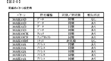
(特徴部30AKに関する説明)
図17は、本実施形態の特徴部30AKに関し、主基板11における一方の基板面(表面)にて、CPU103とRAM102とを接続する配線のパターンが形成された部分の構成例を示している。主基板11では、例えばRAM102とCPU103といった、複数の電気部品を複数の信号配線により接続するために、複数の信号配線を構成する配線のパターンが形成されている。CPU103は、パチンコ遊技機1における遊技の制御に関して、所定の処理を実行可能に構成された電気部品であり、RAM102はCPU103による処理の実行に関する情報を記憶可能に構成された電気部品である。
(Explanation regarding the feature 30AK)
FIG. 17 shows a configuration example of a portion in which a wiring pattern for connecting the
複数の信号配線を構成する配線のパターンに対し、それらの周囲あるいは信号配線間における領域にて、1または複数のグランド導体が配置されている。グランド導体は、基準グランドや特性インピーダンス調整用グランドとして機能し、グランド電圧に維持される。図17に示す構成例では、複数のグランド導体として、複数の信号配線の周囲における領域にグランド導体30AK10Gおよびグランド導体30AK11Gが配置され、複数の信号配線間における領域にグランド導体30AK20Gが配置されている。このように、複数の信号配線を構成する配線のパターンが設けられていない空白領域となる空域部分には、1または複数のグランド導体が設けられていてもよい。これにより、複数の信号配線から放射される電磁波ノイズや信号配線間での電磁波ノイズによる電磁妨害を、防止あるいは抑制できる。 One or a plurality of ground conductors are arranged in the area around or between the signal wirings with respect to the wiring patterns constituting the plurality of signal wirings. The ground conductor functions as a reference ground or a characteristic impedance adjustment ground, and is maintained at the ground voltage. In the configuration example shown in FIG. 17, as a plurality of ground conductors, a ground conductor 30AK10G and a ground conductor 30AK11G are arranged in a region around a plurality of signal wires, and a ground conductor 30AK20G is arranged in a region between the plurality of signal wires. . As described above, one or a plurality of ground conductors may be provided in an airspace portion which is a blank area where a wiring pattern constituting a plurality of signal wirings is not provided. Thereby, the electromagnetic interference by the electromagnetic wave noise radiated | emitted from several signal wiring and the electromagnetic wave noise between signal wiring can be prevented or suppressed.
なお、複数の信号配線の周囲および信号配線間における双方の領域に複数のグランド導体が配置されるものに限定されず、複数の信号配線の周囲または信号配線間における一方の領域にのみグランド導体が配置されるものであってもよい。あるいは、このようなグランド導体が配置されないものであってもよい。 It should be noted that the ground conductor is not limited to one in which a plurality of ground conductors are arranged in both regions around the signal wires and between the signal wires. It may be arranged. Alternatively, such a ground conductor may not be disposed.
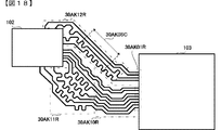
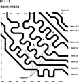
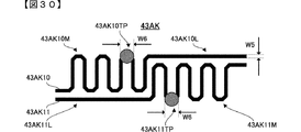
図18は、図17に示した複数の信号配線を構成する配線のパターンについて、より詳細に説明するための領域や区間を示している。図18に示す領域30AK01Rは、複数の信号配線がCPU103に接続される側の端部における領域である。図18に示す領域30AK10Rは、複数の信号配線がいずれも直線形状または略直線形状で互いに平行または略平行な第1形状となる領域であり、図18に示す領域30AK11Rと領域30AK12Rは、少なくとも一部の信号配線が直線形状および略直線形状とは異なる形状で他の信号配線と平行および略平行ではない第2形状となる領域である。図18に示す区間30AK0SCでは、複数の信号配線のうち一部の信号配線が最短または略最短の距離で接続する短距離パターンと短距離パターンに含まれない信号配線が短距離パターンよりも長い距離で接続する長距離パターンとが配置されている。
FIG. 18 shows areas and sections for explaining in more detail the wiring patterns constituting the plurality of signal wirings shown in FIG. A region 30AK01R illustrated in FIG. 18 is a region at an end portion on the side where a plurality of signal wirings are connected to the
図19は、図18に示された領域30AK01Rの拡大図である。図19に示す領域30AK01Rにおいて、複数の信号配線を構成する配線のパターンは、パターン30AK10D〜30AK13Dと、パターン30AK10CKと、パターン30AK10CSと、パターン30AK10RSと、パターン30AK10A〜30AK14Aとを含んでいる。 FIG. 19 is an enlarged view of the region 30AK01R shown in FIG. In the region 30AK01R shown in FIG. 19, the patterns of the wirings constituting the plurality of signal wirings include patterns 30AK10D to 30AK13D, pattern 30AK10CK, pattern 30AK10CS, pattern 30AK10RS, and patterns 30AK10A to 30AK14A.
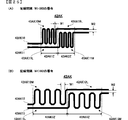
図20は、図19に示された配線のパターンに対応して、信号種類、信号同期の有無、蛇行形状の有無についての設定例を示している。図20に示す信号種類は、各配線のパターンが構成する信号配線で伝送される電気信号の内容(用途)を示している。図20に示す信号同期は、他の信号配線で伝送される電気信号に対する同期の有無を示している。図20に示す蛇行形状は、RAM102とCPU103との間を接続する各配線のパターンについて、直線形状および略直線形状とは異なる蛇行形状となる部分が設けられているか否かを示している。蛇行形状は、ミアンダ形状やジグザグ形状、あるいは折返し形状とも称され、所定区間における信号配線の延設方向に対し、信号配線が繰り返し折り曲げられることにより、例えば延設方向に直交あるいは略直交する方向に折返し往復する形状であればよい。
FIG. 20 shows an example of setting the signal type, the presence / absence of signal synchronization, and the presence / absence of a meandering shape corresponding to the wiring pattern shown in FIG. The signal types shown in FIG. 20 indicate the contents (uses) of electric signals transmitted through the signal wirings formed by the wiring patterns. The signal synchronization shown in FIG. 20 indicates the presence or absence of synchronization with an electric signal transmitted through another signal wiring. The meandering shape shown in FIG. 20 indicates whether or not each wiring pattern connecting the
図20に示す設定例において、配線のパターン30AK10D〜30AK13Dは、いずれもデータ信号を伝送するための信号配線を構成する。各信号配線で伝送されるデータ信号は、例えばクロック信号および他の信号配線で伝送されるデータ信号といった、他の信号配線で伝送される信号と同期して伝送される。配線のパターン30AK10CKは、クロック信号を伝送するための信号配線を構成する。クロック信号は、例えばデータ信号やアドレス信号、チップセレクト信号といった、他の信号配線で伝送される信号と同期して伝送される。配線のパターン30AK10CSは、チップセレクト信号を伝送するための信号配線を構成する。チップセレクト信号は、例えばクロック信号といった、他の信号配線で伝送される信号と同期して伝送される。配線のパターン30AK10RSは、リセット信号を伝送するための信号配線を構成する。リセット信号は、他の信号配線で伝送される信号とは同期しない非同期で伝送される。配線のパターン30AK10A〜30AK14Aは、いずれもアドレス信号を伝送するための信号配線を構成する。各信号配線で伝送されるアドレス信号は、例えばクロック信号および他の信号配線で伝送されるアドレス信号といった、他の信号配線で伝送される信号と同期して伝送される。 In the setting example shown in FIG. 20, all of the wiring patterns 30AK10D to 30AK13D constitute a signal wiring for transmitting a data signal. A data signal transmitted through each signal wiring is transmitted in synchronization with a signal transmitted through another signal wiring, such as a clock signal and a data signal transmitted through another signal wiring. The wiring pattern 30AK10CK constitutes a signal wiring for transmitting a clock signal. The clock signal is transmitted in synchronization with a signal transmitted through another signal wiring such as a data signal, an address signal, and a chip select signal. The wiring pattern 30AK10CS constitutes a signal wiring for transmitting a chip select signal. The chip select signal is transmitted in synchronization with a signal transmitted through another signal wiring, such as a clock signal. The wiring pattern 30AK10RS constitutes a signal wiring for transmitting a reset signal. The reset signal is transmitted asynchronously without being synchronized with a signal transmitted through another signal wiring. Each of the wiring patterns 30AK10A to 30AK14A constitutes a signal wiring for transmitting an address signal. An address signal transmitted through each signal wiring is transmitted in synchronization with a signal transmitted through another signal wiring, such as a clock signal and an address signal transmitted through another signal wiring.
他の信号配線で伝送される信号と同期して伝送されるデータ信号、クロック信号、チップセレクト信号、アドレス信号のうちデータ信号を伝送するための信号配線を構成する配線のパターン30AK10D〜30AK13Dには、蛇行形状がない配線のパターン30AK10Dが含まれている。配線のパターン30AK10Dが構成する信号配線で伝送されるデータ信号とは異なるデータ信号、クロック信号、チップセレクト信号、アドレス信号を伝送するための信号配線を構成する配線のパターンは、少なくとも一部分が直線形状および略直線形状とは異なる形状としての蛇行形状となっている。 The wiring patterns 30AK10D to 30AK13D constituting the signal wiring for transmitting the data signal among the data signal, the clock signal, the chip select signal, and the address signal transmitted in synchronization with the signal transmitted through the other signal wiring include A wiring pattern 30AK10D having no meandering shape is included. At least part of the wiring pattern constituting the signal wiring for transmitting the data signal, clock signal, chip select signal, and address signal different from the data signal transmitted by the signal wiring formed by the wiring pattern 30AK10D is linear. Further, the meandering shape is different from the substantially linear shape.
配線のパターン30AK10Dが構成するデータ信号を伝送するための信号配線は、他のデータ信号、クロック信号、チップセレクト信号、アドレス信号を伝送するための信号配線に比べて、RAM102とCPU103における接続端子間の距離が長くなっている。そこで、配線のパターン30AK10Dが構成する信号配線で伝送されるデータ信号とは異なるデータ信号、クロック信号、チップセレクト信号、アドレス信号を伝送するための信号配線を構成する配線のパターンは、少なくとも一部分が蛇行形状となることにより、各信号配線の配線長が同一または略同一となる。その一方で、配線のパターン30AK10Dには蛇行形状を設ける必要がない。
The signal wiring for transmitting the data signal formed by the wiring pattern 30AK10D is more connected between the connection terminals of the
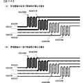
このように、同期信号を伝送するための信号配線のうち複数の電気部品における接続端子間の距離が他の接続端子間の距離と比べて長くなる信号配線は、例えば蛇行形状となる配線部分といった、直線形状および略直線形状とは異なる形状となる配線部分を含まないように、配線のパターンが形成されていればよい。逆にいうと、直線形状または略直線形状などの形状となる一方で蛇行形状のような直線形状および略直線形状とは異なる形状を含まない配線のパターンが構成する信号配線は、蛇行形状のような直線形状および略直線形状とは異なる形状を含む配線のパターンが構成する信号配線と比較して、複数の電気部品における接続端子間の距離が長い。あるいは、同期信号を伝送するための信号配線のうち複数の電気部品における接続端子間の距離が他の接続端子間の距離と比べて長くなる信号配線は、例えば蛇行形状となる配線部分といった、他の信号配線と平行および略平行な形状とは異なる形状となる配線部分を含まないように、配線のパターンが形成されていればよい。逆にいうと、他の信号配線と平行または略平行な形状となる一方で蛇行形状のような平行および略平行な形状とは異なる形状を含まない配線のパターンが構成する信号配線は、蛇行形状のような他の信号配線と平行および略平行な形状とは異なる形状を含む配線のパターンが構成する信号配線と比較して、複数の電気部品における接続端子間の距離が長い。これにより、各信号配線の配線長を同一または略同一とし、複数の信号配線で伝送される信号の遅延時間差(スキュー)が発生することを、防止あるいは抑制できる。複数の信号配線で伝送される信号の遅延時間差を減少させることにより、複数の信号配線で伝送される信号の信頼性を向上させることができる。 Thus, the signal wiring in which the distance between the connection terminals in the plurality of electrical components among the signal wirings for transmitting the synchronization signal is longer than the distance between the other connection terminals is, for example, a wiring portion having a meandering shape. The wiring pattern may be formed so as not to include a wiring portion having a shape different from the linear shape and the substantially linear shape. In other words, the signal wiring formed by the wiring pattern which does not include a linear shape such as a meandering shape or a shape different from the substantially linear shape while having a linear shape or a substantially linear shape is like a meandering shape. The distance between the connection terminals in the plurality of electrical components is longer than the signal wiring formed by the wiring pattern including a shape different from the straight line shape and the substantially straight line shape. Alternatively, among the signal wirings for transmitting the synchronization signal, the signal wiring in which the distance between the connection terminals in the plurality of electrical components is longer than the distance between the other connection terminals is, for example, a wiring portion having a meandering shape. The wiring pattern may be formed so as not to include a wiring portion having a shape different from the shape parallel to and substantially parallel to the signal wiring. In other words, the signal wiring formed by a wiring pattern that is parallel or substantially parallel to other signal wirings but does not include a parallel or substantially parallel shape such as a meandering shape is a meandering shape. The distance between the connection terminals in the plurality of electrical components is longer than the signal wiring formed by the wiring pattern including a shape different from the parallel and substantially parallel shape to the other signal wiring. As a result, it is possible to prevent or suppress the occurrence of a delay time difference (skew) between signals transmitted through a plurality of signal wirings by making the wiring lengths of the respective signal wirings the same or substantially the same. By reducing the delay time difference between signals transmitted through a plurality of signal lines, the reliability of signals transmitted through the plurality of signal lines can be improved.
配線のパターン30AK10RSには、蛇行形状が設けられていない。配線のパターン30AK10RSは、非同期信号であるリセット信号を伝送するための信号配線を構成する。リセット信号などの非同期信号を伝送する場合には、他の信号配線で伝送される信号との遅延時間差を考慮する必要がない。そこで、リセット信号を伝送するための信号配線を構成する配線のパターン30AK10RSのように、非同期信号が伝送される信号配線を構成する配線のパターンには蛇行形状を設けない。配線のパターンに蛇行形状を設けないようにすれば、配線のパターンを配置する基板面積の増大が抑制されて、基板の小型化を図ることができる。 The wiring pattern 30AK10RS is not provided with a meandering shape. The wiring pattern 30AK10RS constitutes a signal wiring for transmitting a reset signal that is an asynchronous signal. When an asynchronous signal such as a reset signal is transmitted, there is no need to consider a delay time difference from a signal transmitted through another signal wiring. Therefore, like the wiring pattern 30AK10RS constituting the signal wiring for transmitting the reset signal, the meandering shape is not provided in the wiring pattern constituting the signal wiring for transmitting the asynchronous signal. If the meandering shape is not provided in the wiring pattern, an increase in the area of the substrate on which the wiring pattern is arranged can be suppressed, and the size of the substrate can be reduced.
蛇行形状を設けない配線のパターンとして、グランド電圧に維持されるダミー配線を構成する配線のパターンが配置されてもよい。例えば配線のパターン30AK10RSが構成する信号配線では、リセット信号が伝送されることに代えて、グランド電圧に維持されてもよい。配線のパターン30AK10RSは、データ信号を伝送するための信号配線を構成する配線のパターン30AK10D〜30AK13D、クロック信号を伝送するための信号配線を構成する配線のパターン30AK10CK、チップセレクト信号を伝送するための信号配線を構成する配線のパターン30AK10CSで構成される一群のパターンと、アドレス信号を伝送するための信号配線を構成する配線のパターン30AK10A〜30AK14Aで構成される一群のパターンとの間に配置されている。配線のパターン30AK10RSのような他の信号配線間に配置される信号配線をグランド電圧に維持されるダミー配線とすることにより、複数の信号配線での電磁波ノイズによる電磁妨害の防止あるいは抑制が図られる。蛇行形状を設けない配線のパターンとしては、グランド電圧に維持されるダミー配線に代えて、あるいはグランド電圧に維持されるダミー配線とともに、電源電圧に維持される配線のパターンが配置されてもよい。例えば配線のパターン30AK10RSが構成する信号配線では、リセット信号が伝送されることに代えて、電源電圧に維持されてもよい。なお、電源電圧に維持される配線のパターンは、他の信号配線を構成する配線のパターンと近接して配置すると、それぞれの信号配線どうしの電磁結合などにより、電磁波ノイズが発生するおそれがある。そこで、電源電圧に維持される配線のパターンを配置する場合には、グランド電圧に維持される配線のパターンを配置する場合と比較して、信号配線からの距離が長くなるように、各配線のパターンが形成されてもよい。これにより、信号配線での電磁波ノイズによる電磁妨害の防止あるいは抑制が図られる。 As a wiring pattern not provided with a meandering shape, a wiring pattern constituting a dummy wiring maintained at the ground voltage may be arranged. For example, in the signal wiring formed by the wiring pattern 30AK10RS, the reset signal may be transmitted and the ground voltage may be maintained. The wiring pattern 30AK10RS includes wiring patterns 30AK10D to 30AK13D constituting a signal wiring for transmitting a data signal, wiring pattern 30AK10CK constituting a signal wiring for transmitting a clock signal, and a chip select signal. Arranged between a group of patterns composed of wiring patterns 30AK10CS constituting the signal wiring and a group of patterns composed of wiring patterns 30AK10A to 30AK14A constituting the signal wiring for transmitting the address signal. Yes. By using a signal wiring arranged between other signal wirings such as the wiring pattern 30AK10RS as a dummy wiring maintained at a ground voltage, electromagnetic interference due to electromagnetic wave noise in a plurality of signal wirings can be prevented or suppressed. . As the wiring pattern not provided with the meandering shape, a wiring pattern maintained at the power supply voltage may be arranged in place of the dummy wiring maintained at the ground voltage or together with the dummy wiring maintained at the ground voltage. For example, in the signal wiring formed by the wiring pattern 30AK10RS, the power supply voltage may be maintained instead of transmitting the reset signal. If the wiring pattern maintained at the power supply voltage is arranged close to the wiring pattern constituting the other signal wirings, electromagnetic wave noise may be generated due to electromagnetic coupling between the signal wirings. Therefore, when the wiring pattern maintained at the power supply voltage is arranged, the distance from the signal wiring is increased as compared with the case where the wiring pattern maintained at the ground voltage is arranged. A pattern may be formed. Thereby, prevention or suppression of electromagnetic interference due to electromagnetic wave noise in the signal wiring can be achieved.
図21は、図18に示された領域30AK10Rの拡大図である。領域30AK10Rには、配線のパターン30AK10CK、30AK10CS、30AK10RS、30AK10A〜14Aが形成されている。これらの配線のパターンは、領域30AK10Rにおいて、複数の信号配線がいずれも直線形状または略直線形状で互いに平行または略平行な形状となるように形成されている。このように、領域30AK10Rでは、複数の信号配線を構成する配線のパターンがいずれも直線形状または略直線形状となるように形成され、複数の信号配線が互いに平行または略平行な形状となるように配線のパターンが形成されている。 FIG. 21 is an enlarged view of the region 30AK10R shown in FIG. In the region 30AK10R, wiring patterns 30AK10CK, 30AK10CS, 30AK10RS, and 30AK10A to 14A are formed. These wiring patterns are formed in the region 30AK10R so that the plurality of signal wirings are all linear or substantially linear and parallel or substantially parallel to each other. As described above, in the region 30AK10R, the wiring patterns constituting the plurality of signal wirings are all formed to have a linear shape or a substantially linear shape, and the plurality of signal wirings have a shape parallel to or substantially parallel to each other. A wiring pattern is formed.
図22は、図18に示された領域30AK11Rの拡大図である。領域30AK11Rには、領域30AK10Rと同じく、配線のパターン30AK10CK、30AK10CS、30AK10RS、30AK10A〜14Aが形成されている。これらの配線のパターンは、領域30AK11Rにおいて、少なくとも1の信号配線が直線形状または略直線形状となるように形成されている一方で、他の信号配線が直線形状および略直線形状とは異なる形状となるように形成されている。図22に示す領域30AK11Rにおいて、例えばクロック信号を伝送するための信号配線を構成する配線のパターン30AK10CK、チップセレクト信号を伝送するための信号配線を構成する配線のパターン30AK10CSは、複数の折り曲げ部を含むものの、いずれも直線形状または略直線形状となるように形成されている。また、図22に示す領域30AK11Rにおいて、リセット信号を伝送するための信号配線を構成する配線のパターン30AK10RSは、折り曲げ部を含まない直線形状または略直線形状となるように形成されている。これに対し、図22に示す領域30AK11Rにおいて、アドレス信号を伝送するための信号配線を構成する配線のパターン30AK10A〜30AK14Aは、複数の折り曲げ部により蛇行形状が形成され、直線形状および略直線形状とは異なる形状となるように形成されている。 FIG. 22 is an enlarged view of the region 30AK11R shown in FIG. Similar to the region 30AK10R, wiring patterns 30AK10CK, 30AK10CS, 30AK10RS, and 30AK10A to 14A are formed in the region 30AK11R. These wiring patterns are formed in the region 30AK11R so that at least one signal wiring has a linear shape or a substantially linear shape, while other signal wirings have shapes different from the linear shape and the substantially linear shape. It is formed to become. In the area 30AK11R shown in FIG. 22, for example, a wiring pattern 30AK10CK constituting a signal wiring for transmitting a clock signal and a wiring pattern 30AK10CS constituting a signal wiring for transmitting a chip select signal have a plurality of bent portions. Although it includes, all are formed so that it may become a linear shape or a substantially linear shape. In addition, in the region 30AK11R shown in FIG. 22, the wiring pattern 30AK10RS constituting the signal wiring for transmitting the reset signal is formed to have a linear shape or a substantially linear shape not including the bent portion. On the other hand, in the area 30AK11R shown in FIG. 22, the wiring patterns 30AK10A to 30AK14A constituting the signal wiring for transmitting the address signal are formed in a meandering shape by a plurality of bent portions, Are formed to have different shapes.
蛇行形状が形成される部分では、例えば複数の折り曲げ部を介することにより、信号配線が本来の延設方向に対して直交する方向へと屈曲されていればよい。各折り曲げ部では、信号配線が直角よりも大きい角度(鈍角)をなすように折り曲げられることにより、信号配線の延設方向が変更された配線のパターンが形成されていればよい。この場合に、各折り曲げ部における折り曲げ量は、直角よりも小さい角度となるように、信号配線が折り曲げられる。蛇行形状が形成される部分では、第1延設方向と、この第1延設方向に対して直交または略直交する第2延設方向とに、信号配線を延設可能とし、第1延設方向の信号配線を構成する配線のパターンと、第2延設方向の信号配線を構成する配線のパターンとの間には、複数の折り曲げ部が設けられていればよい。このように、信号配線の折り曲げ量が所定角度よりも小さい角度となる複数の折り曲げ部を介して信号配線の延設方向が変更される。折り曲げ量を小さくすることにより、折り曲げ部における配線のパターン幅が大きく変化してしまうことを抑制し、伝送路の特性インピーダンスが急変することを防止して、複数の信号配線での電磁波ノイズによる電磁妨害の防止あるいは抑制が図られる。 In the portion where the meandering shape is formed, the signal wiring may be bent in a direction orthogonal to the original extending direction, for example, via a plurality of bent portions. In each bent portion, it is only necessary to form a wiring pattern in which the extending direction of the signal wiring is changed by bending the signal wiring so as to form an angle (obtuse angle) larger than a right angle. In this case, the signal wiring is bent so that the amount of bending at each bent portion is smaller than a right angle. In the portion where the meandering shape is formed, the signal wiring can be extended in the first extending direction and the second extending direction orthogonal to or substantially orthogonal to the first extending direction. A plurality of bent portions may be provided between the wiring pattern constituting the signal wiring in the direction and the wiring pattern constituting the signal wiring in the second extending direction. As described above, the extending direction of the signal wiring is changed through the plurality of bent portions where the bending amount of the signal wiring is smaller than the predetermined angle. By reducing the amount of bending, the pattern width of the wiring at the bent part is prevented from changing greatly, the characteristic impedance of the transmission line is prevented from changing suddenly, and electromagnetic waves due to electromagnetic wave noise in multiple signal wirings are prevented. Interference can be prevented or suppressed.
各信号配線では、折り曲げ部の位置が他の信号配線における折り曲げ部の位置から所定長より長い距離となるように、複数の折り曲げ部が配置されていればよい。所定長は、例えば2mm〜5mmの範囲に含まれる一定長といった、基板設計上の観点から予め定められた長さであればよい。信号配線の折り曲げ部では、特性インピーダンスの変化などにより、電磁波ノイズが発生しやすくなる。複数の信号配線に含まれる1の信号配線を構成する配線のパターンが形成する折り曲げ部は、複数の信号配線に含まれる他の信号配線を構成する配線のパターンが形成する折り曲げ部と接近して配置されると、各信号配線で伝送される信号が電磁波ノイズの影響を受けやすくなるおそれがある。そこで、複数の信号配線に含まれる1の信号配線を構成する配線のパターンが形成する折り曲げ部と、複数の信号配線に含まれる他の信号配線を構成する配線のパターンが形成する折り曲げ部とが、所定長より長い距離となるように間隔をあけて配置することにより、複数の信号配線での電磁波ノイズによる電磁妨害の防止あるいは抑制が図られる。 In each signal wiring, a plurality of bent portions may be arranged so that the positions of the bent portions are longer than a predetermined length from the positions of the bent portions in other signal wirings. The predetermined length may be a predetermined length from the viewpoint of substrate design, for example, a certain length included in a range of 2 mm to 5 mm. In the bent portion of the signal wiring, electromagnetic noise is likely to be generated due to a change in characteristic impedance. The bent portion formed by the wiring pattern constituting one signal wiring included in the plurality of signal wirings approaches the bent portion formed by the wiring pattern constituting another signal wiring included in the plurality of signal wirings. When arranged, the signal transmitted through each signal wiring may be easily affected by electromagnetic noise. Therefore, a bent portion formed by a wiring pattern constituting one signal wiring included in a plurality of signal wirings and a bent portion formed by a wiring pattern constituting another signal wiring included in the plurality of signal wirings are provided. By arranging the gaps at intervals so as to be longer than the predetermined length, it is possible to prevent or suppress electromagnetic interference due to electromagnetic noise in a plurality of signal wirings.
また、領域30AK11Rでは、少なくとも1の信号配線が平行および略平行とは異なる形状となるように形成されている。図22に示す領域30AK11Rにおいて、例えばクロック信号を伝送するための信号配線を構成する配線のパターン30AK10CKと、チップセレクト信号を伝送するための信号配線を構成する配線のパターン30AK10CSは、いずれも複数の折り曲げ部を介しながら、全体として互いの信号配線が平行または略平行な形状となるように形成されている。これに対し、図22に示す領域30AK11Rにおいて、アドレス信号を伝送するための信号配線を構成する配線のパターン30AK10A〜30AK14Aは、複数の折り曲げ部により蛇行形状が形成されているので、全体として互いの信号配線が平行または略平行とは異なる形状となるように形成されている。 In the region 30AK11R, at least one signal wiring is formed to have a shape different from parallel and substantially parallel. In the region 30AK11R shown in FIG. 22, for example, a wiring pattern 30AK10CK constituting a signal wiring for transmitting a clock signal and a wiring pattern 30AK10CS constituting a signal wiring for transmitting a chip select signal are both plural. As a whole, the signal wirings are formed in parallel or substantially in parallel with each other through the bent portion. On the other hand, in the region 30AK11R shown in FIG. 22, the wiring patterns 30AK10A to 30AK14A constituting the signal wiring for transmitting the address signal are formed in a meandering shape by a plurality of bent portions. The signal wiring is formed to have a shape different from parallel or substantially parallel.
図22に示す領域30AK11Rでは、複数の信号配線のうち少なくとも1の信号配線が、平行および略平行な形状とは異なる蛇行形状などの形状となっている。この領域30AK11Rにおいて、信号配線を構成する配線のパターンに近接するスペース領域30AK0SPには、少なくとも信号配線と同一の基板上で導体が設けられていない。スペース領域30AK0SPは、例えばアドレス信号を伝送するための信号配線を構成する配線のパターン30AK10A〜30AK14Aのうち領域30AK11Rにて蛇行形状が設けられた配線のパターン30AK10A〜30AK13Aに近接している。スペース領域30AK0SPには導体が設けられていないことにより、複数の信号配線での電磁波ノイズによる電磁妨害の防止あるいは抑制が図られる。蛇行形状となる配線のパターンに近接する領域に導体が設けられている場合には、信号配線から電磁波が放射される可能性があり、信号配線と導体との電磁結合などにより、電磁波ノイズが発生するおそれがある。そこで、例えばスペース領域30AK0SPのように、蛇行形状が設けられた配線のパターンに近接する領域には導体が設けられないことで、複数の信号配線での電磁波ノイズによる電磁妨害の防止あるいは抑制が図られる。 In the region 30AK11R shown in FIG. 22, at least one signal wiring out of the plurality of signal wirings has a shape such as a meandering shape different from the parallel and substantially parallel shapes. In this region 30AK11R, a conductor is not provided on at least the same substrate as the signal wiring in the space region 30AK0SP close to the wiring pattern constituting the signal wiring. The space area 30AK0SP is close to the wiring patterns 30AK10A to 30AK13A provided with a meandering shape in the area 30AK11R among the wiring patterns 30AK10A to 30AK14A constituting the signal wiring for transmitting the address signal, for example. Since no conductor is provided in the space region 30AK0SP, it is possible to prevent or suppress electromagnetic interference due to electromagnetic wave noise in a plurality of signal wirings. When a conductor is provided in a region close to the meandering wiring pattern, electromagnetic waves may be emitted from the signal wiring, and electromagnetic noise is generated due to electromagnetic coupling between the signal wiring and the conductor. There is a risk. Therefore, for example, a conductor is not provided in a region close to a wiring pattern provided with a meandering shape, such as the space region 30AK0SP, thereby preventing or suppressing electromagnetic interference due to electromagnetic wave noise in a plurality of signal wirings. It is done.
図23は、多層配線基板として形成された主基板11の構成例を示す断面図である。図23に示す主基板11は、合成樹脂を重ねて形成された多層構造を有し、各層の表面または内層には様々な配線のパターンを形成可能とされている。このような多層構造を有する主基板11に形成された配線のパターンを介して、例えばRAM102とCPU103といった、複数の電子部品が電気的に接続される。図23に示す主基板11の多層構造は、表面層30AK1Sと、グランド層30AK1Lと、電源層30AK2Lと、配線層30AK3Lと、電源層30AK4Lと、裏面層30AK2Sとを含んでいる。
FIG. 23 is a cross-sectional view showing a configuration example of the
主基板11における一方の基板面となる表面には、表面層30AK1Sが設けられ、信号配線を構成する配線のパターン30AK10Pおよびパターン30AK11Pが形成されている。主基板11における他方の基板面となる裏面には、裏面層30AK2Sが設けられ、信号配線を構成する配線のパターン30AK20Pが形成されている。主基板11の表面層30AK1Sに形成された配線のパターン30AK10Pは、主基板11の表面層30AK1Sおよび裏面層30AK2Sを貫通するスルーホール30AK1Hを介して、裏面層30AK2Sに形成された配線のパターン30AK20Pと電気的に接続されている。主基板11の表面層30AK1Sに形成された配線のパターン30AK11Pは、主基板11の表面層30AK1Sおよび裏面層30AK2Sを貫通するスルーホール30AK2Hを介して、裏面層30AK2Sに形成された配線のパターン30AK20Pと電気的に接続されている。このように、主基板11には、一方の基板面となる表面に設けられた表面層30AK1Sにおいて信号配線を構成する配線のパターン30AK10Pおよびパターン30AK11Pと、他方の基板面となる裏面に設けられた裏面層30AK2Sにおいて信号配線を構成する配線のパターン30AK20Pとを、電気的に接続可能なスルーホール30AK1Hおよびスルーホール30AK2Hが設けられている。
A surface layer 30AK1S is provided on the surface serving as one of the substrate surfaces of the
図23に示すRAM102とCPU103を接続する複数の信号配線に含まれる各信号配線の配線長は、表面層30AK1Sに形成された配線のパターン30AK10Pおよびパターン30AK11Pと、裏面層30AK2Sに形成された配線のパターン30AK20Pとが構成する信号配線の配線長だけでなく、スルーホール30AK1Hおよびスルーホール30AK2Hの長さを含めて、同一または略同一となる。図23に示す多層構造を有する主基板11において、スルーホール30AK1Hおよびスルーホール30AK2Hの長さを含めて、各信号配線の配線長を同一または略同一とし、複数の信号配線で伝送される信号の遅延時間差が発生することを、防止あるいは抑制できる。主基板11のような多層配線基板において複数の信号配線で伝送される信号の遅延時間差を減少させることにより、複数の信号配線で伝送される信号の信頼性を向上させることができる。
The wiring length of each signal wiring included in the plurality of signal wirings connecting the
図23に示す多層構造を有する主基板11において、表面層30AK1Sに隣接する導体層として、グランド層30AK1Lが設けられている。グランド層30AK1Lには、1または複数のグランド導体が配置され、グランド導体はグランド電圧に維持される。表面層30AK1Sにおいて信号配線を構成する配線のパターン30AK10Pおよびパターン30AK11Pは、少なくともいずれか一方のパターンにおいて、蛇行形状といった、直線形状および略直線形状とは異なる形状で複数の信号配線が平行および略平行な形状とは異なる形状となる領域を含むように形成されていればよい。このような表面層30AK1Sに隣接する導体層としてのグランド層30AK1Lでは、信号の伝送が行われない。配線のパターン30AK10Pおよびパターン30AK11Pが形成された表面層30AK1Sに隣接する導体層で信号の伝送が行われないので、配線のパターン30AK10Pおよびパターン30AK11Pが構成する複数の信号配線で伝送される信号が電磁波ノイズの影響を受けにくくなり、他の信号配線に電磁波ノイズの影響が及ぶことも、防止あるいは抑制できる。
In
図23に示す多層構造を有する主基板11の裏面層30AK2Sにおいて信号配線を構成する配線のパターン30AK20Pが、蛇行形状といった、直線形状および略直線形状とは異なる形状で複数の信号配線が平行および略平行な形状とは異なる形状となる領域を含むように形成されてもよい。このような裏面層30AK2Sに隣接する導体層としての電源層30AK4Lでは、信号の伝送が行われない。電源層30AK4Lには、1または複数の電源導体が配置され、電源導体は電源電圧に維持される。配線のパターン30AK20Pが形成された裏面層30AK2Sに隣接する導体層で信号の伝送が行われないので、配線のパターン30AK20Pが構成する複数の信号配線で伝送される信号が電磁波ノイズの影響を受けにくくなり、他の信号配線に電磁波ノイズの影響が及ぶことも、防止あるいは抑制できる。主基板11のような多層配線基板において複数の信号配線が設けられる層に隣接する導体層では信号の伝送が行われないことにより、複数の信号配線での電磁波ノイズによる電磁妨害の防止あるいは抑制が図られる。
In the back surface layer 30AK2S of the
図23に示す多層構造を有する主基板11の配線層30AK3Lにおいて信号配線を構成する配線のパターンが、蛇行形状といった、直線形状および略直線形状とは異なる形状で複数の信号配線が平行および略平行な形状とは異なる形状となる領域を含むように形成されてもよい。このような配線層30AK3Lに隣接する導体層としての電源層30AK2Lや電源層30AK4Lでは、信号の伝送が行われない。主基板11のような多層配線基板において複数の信号配線が設けられる配線層30AK3Lに隣接する導体層では信号の伝送が行われないことにより、複数の信号配線での電磁波ノイズによる電磁妨害の防止あるいは抑制が図られる。ただし、多層配線基板に設けられた内層の導体層である配線層30AK3Lにおいて信号配線を構成する配線のパターンが蛇行形状などの形状となる領域を含むように形成された場合には、信号配線の断線などによる障害が発生した場合に、配線層30AK3Lにおける信号配線の状態を基板の外部から確認することが困難になるおそれがある。これに対し、主基板11の表面層30AK1Sや裏面層30AK2Sといった、主基板11が備える一方の基板面や他方の基板面において信号配線を構成する配線のパターンが蛇行形状などの形状となる領域を含むように形成された場合には、信号配線の断線などによる障害が発生した場合に、表面層30AK1Sや裏面層30AK2Sにおける信号配線の状態を基板の外部から確認しやすい適切な基板構成が可能になる。
In the wiring layer 30AK3L of the
主基板11の表面層30AK1Sおよび裏面層30AK2Sを貫通するスルーホールは、図23に示すスルーホール30AK1Hおよびスルーホール30AK2Hに限定されず、より多くのスルーホールが設けられ、複数の信号配線における各信号配線の配線長を同一または略同一にするために用いられてもよい。複数の信号配線を構成する配線のパターンのうちには、スルーホール30AK1Hおよびスルーホール30AK2Hのようなスルーホールを介することなく、例えば主基板11の表面層30AK1Sのみに信号配線が配置されるように形成されたパターンが含まれてもよい。配線のパターン30AK10Dが構成するデータ信号を伝送するための信号配線といった、複数の電気部品における接続端子間の距離が他の接続端子間の距離と比べて長くなる信号配線は、スルーホール30AK1Hおよびスルーホール30AK2Hのようなスルーホールを介することなく、主基板11の表面層30AK1Sのみに信号配線が配置されてもよい。逆にいうと、表面層30AK1Sなど1の導体層にてスルーホールを介することなく形成された配線のパターンが構成する信号配線は、表面層30AK1Sおよび裏面層30AK2Sなど複数の導体層にてスルーホールを介して電気的に接続可能となるように形成された配線のパターンが構成する信号配線と比較して、複数の電気部品における接続端子間の距離が長い。
The through holes penetrating the front surface layer 30AK1S and the back surface layer 30AK2S of the
複数の信号配線が隣接して設けられる場合には、図22に示したスペース領域30AK0SPのように、小さな空白領域が形成される。この空白領域にスルーホールを設け、例えばグランド層30AK1Lといった他の導体層と電気的に接続されるように、銅などの導電材料が埋設されたスルーホール電極を有する構成とすることも考えられる。空白領域にスルーホール電極のような導体が設けられる構成では、例えば空白領域における電界分布を安定させるために、多数のスルーホール電極が配置される場合もある。この場合には、主基板11の表面層30AK1Sのみでなく、裏面層30AK2Sにも、例えばバンプといった、スルーホール電極に対応する構造物が配置され、基板上における配線パターンの設計が制約されるという不都合が生じるおそれがある。また、多層配線基板に設けられた内層の導体層であるグランド層30AK1Lや電源層30AK2L、30AK4Lなどでは、スルーホール電極が設けられる場合に、そのスルーホール電極の周囲では導体層のパターンを除去することになり、グランド層30AK1Lや電源層30AK2L、30AK4Lなど内層の導体層におけるパターンが分断され、導体層におけるパターンの設計が困難になるという不都合が生じるおそれがある。さらに、スルーホール電極に代えて、例えばダミーパッドのような導体が空白領域に設けられ、他の導体層とは接続されないような構成では、この導体が外部からの電磁波ノイズによる影響を受けたり、この導体が複数の信号配線に電磁波ノイズの影響を及ぼしたりして、電磁妨害などの悪影響を与える不都合が生じるおそれがある。これに対し、信号配線を構成する配線のパターンに近接するスペース領域30AK0SPには、導体が設けられないことにより、これらの不都合が生じることを、防止あるいは抑制できる。
When a plurality of signal wirings are provided adjacent to each other, a small blank area is formed like the space area 30AK0SP shown in FIG. It is also conceivable that a through hole is provided in this blank region and has a through hole electrode in which a conductive material such as copper is embedded so as to be electrically connected to another conductor layer such as the ground layer 30AK1L. In a configuration in which a conductor such as a through-hole electrode is provided in the blank area, for example, a large number of through-hole electrodes may be arranged in order to stabilize the electric field distribution in the blank area. In this case, not only the surface layer 30AK1S of the
その他、図22に示したスペース領域30AK0SPのように、複数の信号配線が隣接して設けられる場合に形成される空白領域には、例えば基板固定用のネジ穴といった、基板の構成材料とは異なる材料が用いられる構造物が設けられないようにしてもよい。基板固定用のネジ穴が設けられた場合には、ネジ止めにより基板を固定した場合に、ネジの構成材料が外部からの電磁波ノイズによる影響を受け、他の信号配線にも電磁妨害などの悪影響を与える不都合が生じるおそれがある。また、基板に含まれる絶縁層とは誘電率が異なる合成樹脂や誘電材料を用いた構造物、あるいは基板に含まれる導体層とは電気伝導率が異なる合成樹脂や金属材料を用いた構造物が、複数の信号配線に近接した空白領域に設けられた場合には、これらの構造物が外部からの電磁波ノイズによる影響を受けたり、これらの構造物が複数の信号配線に電磁波ノイズの影響を及ぼしたりして、電磁妨害などの悪影響を与える不都合が生じるおそれがある。これに対し、信号配線を構成する配線のパターンに近接するスペース領域30AK0SPなどの空白領域には、基板の構成材料とは異なる材料を用いた構造物が設けられないことにより、これらの不都合が生じることを、防止あるいは抑制できる。 In addition, a blank area formed when a plurality of signal wirings are provided adjacent to each other like a space area 30AK0SP shown in FIG. 22 is different from the constituent material of the board, such as a screw hole for fixing the board. A structure in which the material is used may not be provided. When screw holes for fixing the board are provided, when the board is fixed by screwing, the screw components are affected by electromagnetic noise from the outside, and other signal wirings are also adversely affected by electromagnetic interference. May cause inconvenience. In addition, a structure using a synthetic resin or dielectric material having a dielectric constant different from that of the insulating layer included in the substrate, or a structure using a synthetic resin or metal material having an electric conductivity different from that of the conductor layer included in the substrate. If the structure is provided in a blank area adjacent to a plurality of signal wirings, these structures are affected by electromagnetic noise from the outside, or these structures affect the plurality of signal wirings by electromagnetic noise. May cause inconveniences such as electromagnetic interference. In contrast, blank regions such as the space region 30AK0SP close to the wiring pattern constituting the signal wiring are not provided with a structure using a material different from the constituent material of the substrate. This can be prevented or suppressed.
図18に示す区間30AK0SCでは、データ信号を伝送するための複数の信号配線を形成する配線のパターン30AK10D〜30AK13Dのうち1のパターン30AK13Dが、蛇行形状といった、直線形状および略直線形状とは異なる形状で他の信号配線と平行および略平行な形状とは異なる形状となる信号配線の部分を含むように形成されている。これに対し、少なくともパターン30AK10Dおよびパターン30AK11Dは、区間30AK0SCにて、蛇行形状を含むことなく、直線形状または略直線形状で互いの信号配線が平行または略平行な形状となるように形成されている。したがって、パターン30AK10Dおよびパターン30AK11Dは、信号配線が区間30AK0SCを最短または略最短で接続するパターンとなる。これに対し、パターン30AK12Dおよびパターン30AK13Dは、信号配線が区間30AK0SCをパターン30AK10Dおよびパターン30AK11Dよりも長い距離で接続するパターンとなる。 In section 30AK0SC shown in FIG. 18, one pattern 30AK13D of wiring patterns 30AK10D to 30AK13D forming a plurality of signal wirings for transmitting a data signal is different from a linear shape and a substantially linear shape, such as a meandering shape. Thus, it is formed so as to include a portion of the signal wiring having a shape different from the shape parallel to and substantially parallel to the other signal wiring. On the other hand, at least the pattern 30AK10D and the pattern 30AK11D are formed in the section 30AK0SC so as not to include a meandering shape so that the signal wirings have a linear shape or a substantially linear shape and are parallel or substantially parallel to each other. . Therefore, the pattern 30AK10D and the pattern 30AK11D are patterns in which the signal wiring connects the sections 30AK0SC with the shortest or substantially the shortest. On the other hand, the pattern 30AK12D and the pattern 30AK13D are patterns in which the signal wiring connects the section 30AK0SC with a longer distance than the patterns 30AK10D and 30AK11D.
区間30AK0SCにて、パターン30AK13Dが構成する信号配線が蛇行形状などの直線形状および略直線形状とは異なる形状となっている部分では、他のパターン30AK10D〜パターン30AK12Dが構成する信号配線は直線形状または略直線形状となるように形成されている。このように、複数の信号配線を構成する配線のパターンのうち1の配線のパターンにより構成される信号配線が蛇行形状などの直線形状および略直線形状とは異なる形状となっている部分では、他の配線のパターンにより構成される信号配線が直線形状または略直線形状となるように形成されてもよい。1の配線のパターンにより構成される信号配線が蛇行形状などの直線形状および略直線形状とは異なる形状となる部分は、他の配線のパターンにより構成される信号配線が直線形状または略直線形状となる部分と重複しないように形成されてもよい。蛇行形状などの直線形状および略直線形状とは異なる形状となる部分が、複数の信号配線について重複しないように配線のパターンが形成されることにより、配線のパターンを配置する基板面積の増大が抑制されて、基板の小型化を図ることができる。 In the section 30AK0SC, in the portion where the signal wiring formed by the pattern 30AK13D is different from the linear shape such as a meandering shape and the substantially linear shape, the signal wiring formed by the other patterns 30AK10D to 30AK12D is linear or It is formed to have a substantially linear shape. In this way, in the portion where the signal wiring constituted by one wiring pattern among the wiring patterns constituting the plurality of signal wirings has a shape different from the linear shape such as a meandering shape and the substantially linear shape, The signal wiring constituted by the wiring pattern may be formed in a linear shape or a substantially linear shape. A portion in which a signal wiring constituted by one wiring pattern has a shape different from a linear shape such as a meandering shape and a substantially linear shape indicates that a signal wiring constituted by another wiring pattern has a linear shape or a substantially linear shape. You may form so that it may not overlap with the part which becomes. A wiring pattern is formed so that portions that are different from a linear shape and a substantially linear shape, such as a meandering shape, do not overlap for a plurality of signal wirings, thereby suppressing an increase in the board area on which wiring patterns are arranged Thus, the substrate can be miniaturized.
図24は、複数の信号配線が蛇行形状となる部分が重複しない配線のパターンについて、他の形成例を示している。図24に示す領域30AK20Rでも、複数の信号配線を構成する配線のパターンのうち1の配線パターンにより構成される信号配線が蛇行形状となっている部分では、他の配線のパターンにより構成される信号配線が直線形状または略直線形状となるように形成されている。そして、第1配線のパターンにより構成される第1信号配線が蛇行形状となる部分である第1蛇行部が終了すると、第1配線のパターンとは異なる第2配線のパターンにより構成される第2信号配線が蛇行形状となる部分である第2蛇行部が開始されるように、複数の信号配線を構成する配線のパターンが形成されている。第1蛇行部では、第1信号配線以外の信号配線を構成する配線のパターンとして、第2信号配線を構成する第2配線のパターンを含めた配線のパターンは、各パターンにより構成される信号配線が平行または略平行な形状となるように形成されていればよい。第2蛇行部では、第2信号配線以外の信号配線を構成する配線のパターンとして、第1信号配線を構成する第1配線のパターンを含めた配線のパターンは、各パターンにより構成される信号配線が平行または略平行な形状となるように形成されていればよい。第1蛇行部が終了してから第2蛇行部が開始されるので、第1蛇行部は第2蛇行部と重複しないように配置されている。これにより、多数の信号配線について蛇行形状などの直線形状および略直線形状とは異なる形状となる部分を設けた場合でも、配線のパターンを配置する基板面積の増大が可及的に抑制されて、基板の小型化を図ることができる。 FIG. 24 shows another example of forming a wiring pattern in which portions where a plurality of signal wirings have a meandering shape do not overlap. Also in the region 30AK20R shown in FIG. 24, in the portion where the signal wiring constituted by one wiring pattern among the wiring patterns constituting the plurality of signal wirings has a meandering shape, the signal constituted by the other wiring pattern The wiring is formed in a linear shape or a substantially linear shape. Then, when the first meandering portion, which is a portion where the first signal wiring constituted by the first wiring pattern has a meandering shape, ends, the second wiring constituted by the second wiring pattern different from the first wiring pattern. A pattern of wirings constituting a plurality of signal wirings is formed so that the second meandering part, which is a part where the signal wirings have a meandering shape, is started. In the first meandering portion, the wiring pattern including the second wiring pattern constituting the second signal wiring is the signal wiring constituted by each pattern as the wiring pattern constituting the signal wiring other than the first signal wiring. May be formed so as to have a parallel or substantially parallel shape. In the second meandering portion, the wiring pattern including the first wiring pattern constituting the first signal wiring is the signal wiring constituted by each pattern as the wiring pattern constituting the signal wiring other than the second signal wiring. May be formed so as to have a parallel or substantially parallel shape. Since the second meandering portion is started after the end of the first meandering portion, the first meandering portion is arranged so as not to overlap the second meandering portion. Thereby, even when a portion that is different from a linear shape and a substantially linear shape such as a meandering shape for a large number of signal wirings is provided, an increase in the substrate area on which the wiring pattern is arranged is suppressed as much as possible. The size of the substrate can be reduced.
(特徴部42AKに関する説明)
図25は、本実施形態の特徴部42AKに関し、配線のパターンにより構成される複数の信号配線が形成された部分の構成例を示している。図25に示す配線のパターンは、例えば主基板11にて、RAM102とCPU103といった、複数の電気部品を接続する複数の信号配線を構成するものであればよい。図25に示す構成例では、複数の信号配線を構成する配線のパターンとして、2つの信号配線を構成する配線のパターンが示されている。図25(A)は配線間隔W1が配線間隔W2よりも狭いW1<W2の場合を示し、図25(B)は配線間隔W1が配線間隔W2よりも広いW1>W2の場合を示している。配線間隔W1は、同一の信号配線が蛇行形状となる部分における配線のパターンによる配線間隔である。配線間隔W2は、平行または略平行に隣接して互いに異なる信号配線を構成する配線のパターンどうしによる配線間隔である。
(Explanation regarding feature 42AK)
FIG. 25 shows a configuration example of a portion where a plurality of signal wirings configured by wiring patterns are formed with respect to the characteristic portion 42AK of the present embodiment. The wiring pattern shown in FIG. 25 only needs to constitute a plurality of signal wirings for connecting a plurality of electrical components such as the
図25(A)に示す2つの信号配線を構成する配線のパターンは、配線の第1パターン42AK10と、配線の第2パターン42AK11とを含んでいる。配線の第1パターン42AK10および配線の第2パターン42AK11は、それらの配線のパターンにより構成される信号配線の形状に応じて、配線部42AK1Zと、配線部42AK2Zとが含まれるように、各信号配線を形成している。 The wiring pattern constituting the two signal wirings shown in FIG. 25A includes a first wiring pattern 42AK10 and a second wiring pattern 42AK11. The first wiring pattern 42AK10 and the second wiring pattern 42AK11 are arranged so that each of the signal wirings includes a wiring portion 42AK1Z and a wiring portion 42AK2Z according to the shape of the signal wiring constituted by the wiring patterns. Is forming.
配線部42AK1Zでは、配線の第1パターン42AK10により構成される信号配線が第2形状部42AK10Mを形成し、配線の第2パターン42AK11により構成される信号配線が第1形状部42AK11Lを形成している。配線部42AK2Zでは、配線の第1パターン42AK10により構成される信号配線が第1形状部42AK10Lを形成し、配線の第2パターン42AK11により構成される信号配線が第2形状部42AK11Mを形成している。第1形状部42AK10L、42AK11Lは、信号配線が直線形状または略直線形状の第1形状となるように形成されている。第2形状部42AK10M、42AK11Mは、信号配線が蛇行形状といった、直線形状および略直線形状とは異なる第2形状となるように形成されている。なお、第2形状部42AK10M、42AK11Mは、蛇行形状に限定されず、直線形状および略直線形状とは異なる任意の形状となるように形成されていればよい。 In the wiring part 42AK1Z, the signal wiring constituted by the first wiring pattern 42AK10 forms the second shape part 42AK10M, and the signal wiring constituted by the second wiring pattern 42AK11 forms the first shape part 42AK11L. . In the wiring portion 42AK2Z, the signal wiring constituted by the first wiring pattern 42AK10 forms the first shape portion 42AK10L, and the signal wiring constituted by the second wiring pattern 42AK11 forms the second shape portion 42AK11M. . The first shape portions 42AK10L and 42AK11L are formed so that the signal wiring has a linear shape or a substantially linear first shape. The second shape portions 42AK10M and 42AK11M are formed so that the signal wiring has a second shape different from the linear shape and the substantially linear shape, such as a meandering shape. In addition, 2nd shape part 42AK10M and 42AK11M are not limited to a meandering shape, What is necessary is just to be formed so that it may become arbitrary shapes different from a linear shape and a substantially linear shape.
このように、配線の第1パターン42AK10および配線の第2パターン42AK11により構成される複数の信号配線は、配線部42AK1Zにて、配線の第2パターン42AK11により構成される信号配線が、直線形状または略直線形状の第1形状となる第1形状部42AK11Lに対応して、配線の第1パターン42AK10により構成される信号配線が、第1形状部42AK11Lとは異なる蛇行形状などの第2形状となる第2形状部42AK10Mを含んでいる。すなわち、配線部42AK1Zでは、配線の第2パターン42AK11により構成される信号配線における第1形状部42AK11Lに対応して、配線の第1パターン42AK10により構成される信号配線が第2形状部42AK11Mを含んでいる。 As described above, the plurality of signal wirings configured by the first wiring pattern 42AK10 and the second wiring pattern 42AK11 are formed in the wiring portion 42AK1Z, and the signal wiring configured by the second wiring pattern 42AK11 is linear or Corresponding to the first shape portion 42AK11L, which is a substantially linear first shape, the signal wiring configured by the first pattern 42AK10 of the wiring has a second shape such as a meandering shape different from the first shape portion 42AK11L. The second shape portion 42AK10M is included. That is, in the wiring portion 42AK1Z, the signal wiring constituted by the first wiring pattern 42AK10 includes the second shape portion 42AK11M corresponding to the first shape portion 42AK11L in the signal wiring constituted by the second wiring pattern 42AK11. It is out.
また、配線の第1パターン42AK10および配線の第2パターン42AK11により構成される複数の信号配線は、配線部42AK2Zにて、配線の第1パターン42AK10により構成される信号配線が、直線形状または略直線形状の第1形状となる第1形状部42AK10Lに対応して、配線の第2パターン42AK11により構成される信号配線が、第1形状部42AK10Lとは異なる蛇行形状などの第2形状となる第2形状部42AK11Mを含んでいる。すなわち、配線部42AK2Zでは、配線の第1パターン42AK10により構成される信号配線における第1形状部42AK10Lに対応して、配線の第2パターン42AK11により構成される信号配線が第2形状部42AK11Mを含んでいる。 In addition, a plurality of signal wirings configured by the first wiring pattern 42AK10 and the second wiring pattern 42AK11 are linear or substantially straight at the wiring portion 42AK2Z. Corresponding to the first shape portion 42AK10L that is the first shape of the shape, the signal wiring constituted by the second pattern 42AK11 of the wiring has a second shape such as a meandering shape different from the first shape portion 42AK10L. The shape portion 42AK11M is included. That is, in the wiring portion 42AK2Z, the signal wiring constituted by the second pattern 42AK11 of the wiring includes the second shape portion 42AK11M corresponding to the first shape portion 42AK10L in the signal wiring constituted by the first pattern 42AK10 of the wiring. It is out.
図25(A)に示す信号配線が蛇行形状などの第2形状となる第2形状部42AK10Mおよび第2形状部42AK11Mは、第2形状部42AK10Mが配線部42AK1Zに含まれ、第2形状部42AK11Mが配線部42AK2Zに含まれるように形成されている。これにより、第2形状部42AK10Mおよび第2形状部42AK11Mは、それぞれの配置が互いに重複しない。加えて、各信号配線の配線長は同一または略同一となるように形成されている。このような第2形状部42AK10Mと第2形状部42AK11Mとが含まれるように、配線の第1パターン42AK10および配線の第2パターン42AK11により構成される信号配線が形成されているので、配線のパターンを配置する基板面積の増大が抑制されて、基板の小型化を図ることができる。 In the second shape portion 42AK10M and the second shape portion 42AK11M in which the signal wiring shown in FIG. 25A has a second shape such as a meandering shape, the second shape portion 42AK10M is included in the wiring portion 42AK1Z, and the second shape portion 42AK11M. Is included in the wiring portion 42AK2Z. Thereby, arrangement | positioning of 2nd shape part 42AK10M and 2nd shape part 42AK11M does not mutually overlap. In addition, the wiring length of each signal wiring is formed to be the same or substantially the same. Since the signal wiring constituted by the first pattern 42AK10 of wiring and the second pattern 42AK11 of wiring is formed so as to include the second shape part 42AK10M and the second shape part 42AK11M, the wiring pattern An increase in the area of the substrate on which the substrate is disposed is suppressed, and the substrate can be reduced in size.
図25(B)に示す2つの信号配線を構成する配線のパターンは、配線の第3パターン42AK12と、配線の第4パターン42AK13とを含んでいる。配線の第3パターン42AK12および配線の第4パターン42AK13は、それらの配線のパターンにより構成される信号配線の形状に応じて、配線部42AK3Zと、配線部42AK4Zとが含まれるように、各信号配線を形成している。 The wiring pattern constituting the two signal wirings shown in FIG. 25B includes a third wiring pattern 42AK12 and a fourth wiring pattern 42AK13. The third wiring pattern 42AK12 and the fourth wiring pattern 42AK13 are arranged so that each of the signal wirings includes a wiring part 42AK3Z and a wiring part 42AK4Z according to the shape of the signal wiring constituted by the wiring patterns. Is forming.
配線の第3パターン42AK12および配線の第4パターン42AK13により構成される信号配線は、配線部42AK3Zにて、配線の第4パターン42AK13により構成される信号配線が、直線形状または略直線形状の第1形状となる第1形状部42AK13Lに対応して、配線の第3パターン42AK12により構成される信号配線が、第1形状部42AK13Lとは異なる蛇行形状などの第2形状となる第2形状部42AK12Mを含んでいる。すなわち、配線部42AK3Zでは、配線の第4パターン42AK13により構成される信号配線における第1形状部42AK13Lに対応して、配線の第3パターン42AK12により構成される信号配線が第2形状部42AK12Mを含んでいる。 The signal wiring constituted by the third wiring pattern 42AK12 and the fourth wiring pattern 42AK13 is a first or substantially linear signal wiring constituted by the fourth wiring pattern 42AK13 in the wiring portion 42AK3Z. Corresponding to the first shape portion 42AK13L having the shape, the signal wiring constituted by the third pattern 42AK12 of the wiring has the second shape portion 42AK12M having a second shape such as a meandering shape different from the first shape portion 42AK13L. Contains. That is, in the wiring portion 42AK3Z, the signal wiring constituted by the third wiring pattern 42AK12 includes the second shape portion 42AK12M in correspondence with the first shape portion 42AK13L in the signal wiring constituted by the fourth pattern 42AK13 of the wiring. It is out.
また、配線の第3パターン42AK12および配線の第4パターン42AK13により構成される信号配線は、配線部42AK4Zにて、配線の第3パターン42AK12により構成される信号配線が、直線形状または略直線形状の第1形状となる第1形状部42AK12Lに対応して、配線の第4パターン42AK13により構成される信号配線が、第1形状部42AK12Lとは異なる蛇行形状などの第2形状となる第2形状部42AK13Mを含んでいる。すなわち、配線部42AK4Zでは、配線の第3パターン42AK12により構成される信号配線における第1形状部42AK12Lに対応して、配線の第4パターン42AK13により構成される信号配線が第2形状部42AK13Mを含んでいる。 The signal wiring constituted by the third wiring pattern 42AK12 and the fourth wiring pattern 42AK13 has a linear shape or a substantially linear shape at the wiring portion 42AK4Z. Corresponding to the first shape portion 42AK12L having the first shape, the signal wiring constituted by the fourth pattern 42AK13 of the wiring has a second shape portion having a second shape such as a meandering shape different from the first shape portion 42AK12L. 42AK13M is included. That is, in the wiring part 42AK4Z, the signal wiring constituted by the fourth pattern 42AK13 of the wiring includes the second shape part 42AK13M corresponding to the first shape part 42AK12L in the signal wiring constituted by the third pattern 42AK12 of the wiring. It is out.
図25(B)に示す信号配線が蛇行形状などの第2形状となる第2形状部42AK12Mおよび第2形状部42AK13Mは、第2形状部42AK12Mが配線部42AK3Zに含まれ、第2形状部42AK13Mが配線部42AK4Zに含まれるように形成されている。これにより、第2形状部42AK12Mおよび第2形状部42AK13Mは、それぞれの配置が互いに重複しない。加えて、各信号配線の配線長は同一または略同一となるように形成されている。このような第2形状部42AK12Mと第2形状部42AK13Lとが含まれるように、配線の第3パターン42AK12および配線の第4パターン42AK13により構成される信号配線が形成されているので、配線のパターンを配置する基板面積の増大が抑制されて、基板の小型化を図ることができる。 In the second shape portion 42AK12M and the second shape portion 42AK13M in which the signal wiring shown in FIG. 25B has a second shape such as a meandering shape, the second shape portion 42AK12M is included in the wiring portion 42AK3Z, and the second shape portion 42AK13M. Is included in the wiring portion 42AK4Z. Thereby, arrangement | positioning of 2nd shape part 42AK12M and 2nd shape part 42AK13M does not mutually overlap. In addition, the wiring length of each signal wiring is formed to be the same or substantially the same. Since the signal wiring constituted by the third wiring pattern 42AK12 and the fourth wiring pattern 42AK13 is formed so as to include the second shape portion 42AK12M and the second shape portion 42AK13L, the wiring pattern An increase in the area of the substrate on which the substrate is disposed is suppressed, and the substrate can be reduced in size.
図25(A)に示す構成例では、配線間隔W1よりも配線間隔W2の方が広くなるように、各信号配線が形成されている。例えば第2形状部42AK10Mや第2形状部42AK11Mでは、折り曲げ部により折り返された同一の信号配線が配線間隔W1で往復する蛇行形状を形成しているのに対し、配線の第1パターン42AK10により構成される信号配線と配線の第2パターン42AK11により構成される信号配線とが互いに平行または略平行であるときに隣接する信号配線どうしの配線間隔W2は、配線間隔W1よりも広くなるように、各信号配線が形成されている。このように、同一の信号配線における配線間隔W1よりも隣接する信号配線どうしの配線間隔W2の方が広くなるので、1の信号配線にて発生した短絡などによる悪影響が、他の信号配線にて伝送される信号に及ぶことを、防止あるいは抑制できる。 In the configuration example shown in FIG. 25A, each signal wiring is formed so that the wiring interval W2 is wider than the wiring interval W1. For example, in the second shape portion 42AK10M and the second shape portion 42AK11M, the same signal wiring folded back by the bending portion forms a meandering shape that reciprocates at a wiring interval W1, whereas the second shape portion 42AK10M is configured by the first pattern 42AK10 of the wiring. When the signal wiring to be formed and the signal wiring constituted by the second pattern 42AK11 of the wiring are parallel or substantially parallel to each other, the wiring interval W2 between the adjacent signal wirings is set to be wider than the wiring interval W1. Signal wiring is formed. As described above, since the wiring interval W2 between adjacent signal wirings is wider than the wiring interval W1 in the same signal wiring, adverse effects due to a short circuit or the like occurring in one signal wiring may be caused in other signal wirings. It is possible to prevent or suppress the signal from being transmitted.
図25(B)に示す構成例では、配線間隔W1よりも配線間隔W2の方が狭くなるように、各信号配線が形成されている。例えば第2形状部42AK12Mや第2形状部42AK13Mでは、折り曲げ部により折り返された同一の信号配線が配線間隔W1で往復する蛇行形状を形成しているのに対し、配線の第3パターン42AK12により構成される信号配線と配線の第4パターン42AK13により構成される信号配線とが互いに平行または略平行であるときに隣接する信号配線どうしの配線間隔W2は、配線間隔W1よりも狭くなるように、各信号配線が形成されている。このように、同一の信号配線における配線間隔W1よりも隣接する信号配線どうしの配線間隔W2の方が狭くなるので、1の信号配線の内部における短絡よりも、1の信号配線と他の信号配線との間における短絡の方が、発生しやすくなる。1の信号配線と他の信号配線との間で発生した短絡は、各信号配線に設けられたテストポイントを用いて容易に検出することができる。例えば各信号配線に設けられたテストポイントにテストプローブを接触させて信号配線の電気特性検査を行うことにより、1の信号配線と他の信号配線との間で発生した短絡を検出することができる。 In the configuration example shown in FIG. 25B, each signal wiring is formed so that the wiring interval W2 is narrower than the wiring interval W1. For example, in the second shape portion 42AK12M and the second shape portion 42AK13M, the same signal wiring folded back by the bent portion forms a meandering shape that reciprocates at the wiring interval W1, whereas the second shape portion 42AK12M is configured by the third pattern 42AK12 of the wiring. When the signal wiring and the signal wiring constituted by the fourth pattern 42AK13 of the wiring are parallel or substantially parallel to each other, the wiring interval W2 between the adjacent signal wirings is set to be narrower than the wiring interval W1. Signal wiring is formed. Thus, since the wiring interval W2 between adjacent signal wirings is narrower than the wiring interval W1 in the same signal wiring, one signal wiring and another signal wiring are shorter than a short circuit inside one signal wiring. A short circuit between the two is more likely to occur. A short circuit generated between one signal wiring and another signal wiring can be easily detected using a test point provided in each signal wiring. For example, a short circuit between one signal wiring and another signal wiring can be detected by bringing a test probe into contact with a test point provided in each signal wiring and conducting an electrical characteristic inspection of the signal wiring. .
図25(A)に示すように、一方では、配線の第2パターン42AK11により構成される信号配線が第1形状部42AK11Lを形成している配線部42AK1Zに対応して、配線の第1パターン42AK10により構成される信号配線が第2形状部42AK10Mを形成している。他方では、配線の第1パターン42AK10により構成される信号配線が第1形成部42AK10Lを形成している配線部42AK1Zに対応して、配線の第2パターン42AK11により構成される信号配線が第2形状部42AK11Mを形成している。図25(B)に示すように、一方では、配線の第4パターン42AK13により構成される信号配線が第1形状部42AK13Lを形成している配線部42AK3Zに対応して、配線の第3パターン42AK12により構成される信号配線が第2形状部42AK12Mを形成している。他方では、配線の第3パターン42AK12により構成される信号配線が第1形状部42AK12Lを形成している配線部42AK4Zに対応して、配線の第4パターン42AK13により構成される信号配線が第2形状部42AK13Mを形成している。各配線のパターンにより構成される各信号配線の対応関係は、例えば主基板11などの基板面に垂直な方向からみて、上下関係、左右関係、あるいは所定距離未満の範囲内といった、予め定めた任意の位置範囲内にある信号配線であれば成立し、そのような位置範囲内にない信号配線であれば不成立となる関係であればよい。
As shown in FIG. 25A, on the other hand, the signal wiring constituted by the wiring second pattern 42AK11 corresponds to the wiring part 42AK1Z forming the first shape part 42AK11L, and the wiring first pattern 42AK10. The signal wiring constituted by forms the second shape portion 42AK10M. On the other hand, the signal wiring constituted by the first pattern 42AK10 of the wiring corresponds to the wiring part 42AK1Z forming the first formation part 42AK10L, and the signal wiring constituted by the second pattern 42AK11 of the wiring has the second shape. Part 42AK11M is formed. As shown in FIG. 25B, on the other hand, the signal wiring constituted by the wiring fourth pattern 42AK13 corresponds to the wiring part 42AK3Z forming the first shape part 42AK13L, and the wiring third pattern 42AK12. The signal wiring constituted by forms the second shape portion 42AK12M. On the other hand, the signal wiring constituted by the third pattern 42AK12 of the wiring corresponds to the wiring part 42AK4Z forming the first shape part 42AK12L, and the signal wiring constituted by the fourth pattern 42AK13 of the wiring has the second shape. Part 42AK13M is formed. The correspondence of each signal wiring constituted by the pattern of each wiring is, for example, a predetermined arbitrary relationship such as a vertical relationship, a horizontal relationship, or a range less than a predetermined distance when viewed from a direction perpendicular to the substrate surface such as the
図25(A)や図25(B)に示す例では、1の配線のパターンにより構成される信号配線における第1形状部に対応して他の配線のパターンにより構成される信号配線が第2形状を形成している配線部と、他の配線のパターンにより構成される信号配線における第1形状部に対応して1の配線のパターンにより構成される信号配線が第2形状を形成している配線部とにおいて、配線間隔W1が共通であり配線間隔W2も共通となるように、各信号配線が形成されている。より具体的には、図25(A)に示す配線の第2パターン42AK11により構成される信号配線における第1形状部42AK11Lに対応して、配線の第1パターン42AK10により構成される信号配線が第2形状部42AK10Mを形成している配線部42AK1Zと、配線の第1パターン42AK10により構成される信号配線における第1形状部42AK10Lに対応して、配線の第2パターン42AK11により構成される信号配線が第2形状部42AK11Mを形成している配線部42AK2Zとにおいて、配線間隔W1が共通(一定)であり配線間隔W2も共通(一定)となるように、各信号配線が形成されている。これにより、基板面における配線のパターン設計が容易になる。また、複数の信号配線における形状の相違が抑制されるので、各信号配線における特性インピーダンスのばらつきを抑制して、複数の信号配線における信号品質の均質化が図られる。 In the example shown in FIG. 25A or FIG. 25B, the signal wiring constituted by other wiring patterns corresponding to the first shape portion in the signal wiring constituted by one wiring pattern is the second. A signal wiring constituted by one wiring pattern corresponding to the first shape portion in the signal wiring constituted by the wiring portion forming the shape and another wiring pattern forms the second shape. In the wiring portion, each signal wiring is formed so that the wiring interval W1 is common and the wiring interval W2 is also common. More specifically, the signal wiring constituted by the first pattern 42AK10 of the wiring corresponds to the first shape portion 42AK11L in the signal wiring constituted by the second pattern 42AK11 of the wiring shown in FIG. Corresponding to the first shape portion 42AK10L in the signal wiring constituted by the wiring portion 42AK1Z forming the two shape portions 42AK10M and the first pattern 42AK10 of the wiring, the signal wiring constituted by the second pattern 42AK11 of the wiring is provided. Each signal wiring is formed so that the wiring interval W1 is common (constant) and the wiring interval W2 is also common (constant) with the wiring portion 42AK2Z forming the second shape portion 42AK11M. This facilitates wiring pattern design on the substrate surface. In addition, since the difference in shape among the plurality of signal wirings is suppressed, variation in characteristic impedance among the signal wirings is suppressed, and the signal quality in the plurality of signal wirings can be made uniform.
なお、1の配線のパターンにより構成される信号配線における第1形状部に対応して他の配線のパターンにより構成される信号配線が第2形状を形成している配線部と、他の配線のパターンにより構成される信号配線における第1形状部に対応して1の配線のパターンにより構成される信号配線が第2形状を形成している配線部とでは、配線間隔W1と配線間隔W2の一方または双方が相違するように、各信号配線が形成されてもよい。例えば図25(A)に示す配線部42AK1Zと配線部42AK2Zとにおいて、配線間隔W2は共通とする一方で、配線間隔W1は配線部42AK1Zよりも配線部42AK2Zの方が広くなるように、各信号配線が形成されてもよい。こうした場合には、基板面における配線のパターン設計を柔軟に行うことができる。 In addition, the signal wiring constituted by the pattern of the other wiring corresponding to the first shape portion of the signal wiring constituted by the pattern of the one wiring forms the second shape and the wiring portion of the other wiring. One of the wiring interval W1 and the wiring interval W2 is a wiring portion in which the signal wiring formed by the pattern of one wiring forms the second shape corresponding to the first shape portion in the signal wiring formed by the pattern. Or each signal wiring may be formed so that both may differ. For example, in the wiring portion 42AK1Z and the wiring portion 42AK2Z shown in FIG. 25A, the wiring interval W2 is made common, while the wiring interval W1 is larger in the wiring portion 42AK2Z than in the wiring portion 42AK1Z. A wiring may be formed. In such a case, the wiring pattern design on the substrate surface can be flexibly performed.
図26は、配線のパターンにより構成される複数の信号配線における第2形状部が異なる方向に形成されている構成例を示している。図26(A)に示す構成例では、複数の信号配線を構成する配線のパターンとして、3つの信号配線を構成する配線のパターンが示されている。図26(B)に示す構成例では、複数の信号配線を構成する配線のパターンとして、4つの信号配線を構成する配線のパターンが示されている。 FIG. 26 shows a configuration example in which the second shape portions of a plurality of signal wirings configured by wiring patterns are formed in different directions. In the configuration example shown in FIG. 26A, wiring patterns constituting three signal wirings are shown as wiring patterns constituting a plurality of signal wirings. In the configuration example shown in FIG. 26B, the wiring patterns constituting the four signal wirings are shown as the wiring patterns constituting the plurality of signal wirings.
図26(A)に示す3つの信号配線を構成する配線のパターンは、配線の第1パターン42AK20、配線の第2パターン42AK21、配線の第3パターン42AK22を含んでいる。配線の第1パターン42AK20により構成される信号配線は、第2形状部42AK20Mを形成する部分を含んでいる。配線の第2パターン42AK21により構成される信号配線は、第2形状部42AK21Mを形成する部分を含んでいる。配線の第3パターン42AK22により構成される信号配線は、第2形状部42AK22Mを形成する部分を含んでいる。第2形状部42AK20Mおよび第2形状部42AK21Mは、例えば左右方向といった、第1方向に折返し往復する蛇行形状を有している。これに対し、第2形状部42AK22Mは、例えば上下方向といった、第1方向とは異なる第2方向に折返し往復する蛇行形状を有している。なお、それぞれの第2形状部は、蛇行形状に限定されず、直線形状および略直線形状とは異なる任意の形状となるように形成されていればよい。 A wiring pattern constituting the three signal wirings shown in FIG. 26A includes a first wiring pattern 42AK20, a second wiring pattern 42AK21, and a third wiring pattern 42AK22. The signal wiring constituted by the first wiring pattern 42AK20 includes a portion for forming the second shape portion 42AK20M. The signal wiring constituted by the second pattern 42AK21 of the wiring includes a portion for forming the second shape portion 42AK21M. The signal wiring constituted by the third wiring pattern 42AK22 includes a portion for forming the second shape portion 42AK22M. The second shape portion 42AK20M and the second shape portion 42AK21M have a meandering shape that reciprocates in the first direction such as the left-right direction. On the other hand, the second shape portion 42AK22M has a meandering shape that turns back and forth in a second direction different from the first direction, for example, the up-down direction. In addition, each 2nd shape part is not limited to a meandering shape, What is necessary is just to be formed so that it may become arbitrary shapes different from a linear shape and a substantially linear shape.
このように、配線の第1パターン42AK20により構成される信号配線における第2形状部42AK20Mは、配線の第2パターン42AK21により構成される信号配線における第2形状部42AK21Mと共通(平行)な第1方向に形成されている。これに対し、配線の第3パターン42AK22により構成される信号配線における第2形状部42AK22Mは、配線の第1パターンにより構成される第2形状部42AK20Mや配線の第2パターンにより構成される第2形状部42AK21Mが形成される第1方向とは異なる第2方向に形成されている。複数の信号配線において異なる方向に第2形状部が形成されるようにしたことにより、基板面における配線のパターン設計を容易かつ柔軟に行うことができる。また、配線のパターンを配置する基板面積の増大が抑制されて、基板の小型化を図ることができる。 As described above, the second shape portion 42AK20M in the signal wiring constituted by the first pattern 42AK20 of wiring is the first (common) parallel (parallel) to the second shape portion 42AK21M in the signal wiring constituted by the second pattern 42AK21 of wiring. It is formed in the direction. On the other hand, the second shape part 42AK22M in the signal wiring constituted by the third wiring pattern 42AK22 is the second shape part 42AK20M constituted by the first pattern of wiring and the second shape constituted by the second pattern of wiring. It is formed in a second direction different from the first direction in which the shape portion 42AK21M is formed. Since the second shape portions are formed in different directions in the plurality of signal wirings, the wiring pattern design on the substrate surface can be easily and flexibly performed. Further, an increase in the area of the substrate on which the wiring pattern is arranged is suppressed, and the substrate can be reduced in size.
図26(B)に示す4つの信号配線を構成する配線のパターンは、配線の第4パターン42AK23、配線の第5パターン42AK24、配線の第6パターン42AK25、配線の第7パターン42AK26を含んでいる。配線の第4パターン42AK23により構成される信号配線は、2つの第2形状部42AK23M1、42AK23M2を形成する部分を含んでいる。配線の第5パターン42AK24により構成される信号配線は、1つの第2形状部42AK24Mを形成する部分を含んでいる。配線の第6パターン42AK25により構成される信号配線は、1つの第2形状部42AK25Mを形成する部分を含んでいる。配線の第7パターン42AK26により構成される信号配線は、2つの第2形状部42AK26M1、42AK26M2を形成する部分を含んでいる。図26(B)に示す複数の第2形状部のうち、第2形状部42AK23M1、42AK25M、42AK26M2は、例えば上下方向といった、第1方向に折返し往復する蛇行形状を有している。これに対し、第2形状部42AK23M2、42AK24M、42AK26M1は、例えば左右方向といった、第1方向とは異なる第2方向に折返し往復する蛇行形状を有している。 The wiring patterns constituting the four signal wirings shown in FIG. 26B include a fourth wiring pattern 42AK23, a fifth wiring pattern 42AK24, a sixth wiring pattern 42AK25, and a seventh wiring pattern 42AK26. . The signal wiring constituted by the fourth pattern 42AK23 of the wiring includes a portion for forming two second shape portions 42AK23M1 and 42AK23M2. The signal wiring constituted by the fifth pattern 42AK24 of wiring includes a portion for forming one second shape portion 42AK24M. The signal wiring constituted by the sixth pattern 42AK25 of wiring includes a portion for forming one second shape portion 42AK25M. The signal wiring constituted by the seventh wiring pattern 42AK26 includes a portion for forming two second shape portions 42AK26M1 and 42AK26M2. Among the plurality of second shape portions shown in FIG. 26B, the second shape portions 42AK23M1, 42AK25M, and 42AK26M2 have a meandering shape that folds back and forth in the first direction, for example, the vertical direction. On the other hand, the second shape portions 42AK23M2, 42AK24M, and 42AK26M1 have meandering shapes that reciprocate in a second direction different from the first direction, such as the left-right direction.
図26(B)に示すように、配線のパターンにより構成される複数の信号配線には、1つの第2形状部を形成する部分を含む信号配線と、複数の第2形状部を形成する部分を含む信号配線とがあってもよい。あるいは、配線のパターンにより構成される複数の信号配線は、各信号配線が1つの第2形状部を形成する部分のみを含んでいてもよい。あるいは、配線のパターンにより構成される複数の信号配線は、各信号配線が複数の第2形状部を形成する部分を含んでいてもよい。図26(B)に示す配線の第4パターン42AK23により構成される信号配線における第2形状部42AK23M1は、配線の第6パターン42AK25により構成される信号配線における第2形状部42AK25Mや配線の第7パターン42AK26により構成される信号配線における第2形状部42AK26M2と共通(平行)な第1方向に形成されている。また、配線の第4パターン42AK23により構成される信号配線における第2形状部42AK23M2は、配線の第5パターン42AK24により構成される信号配線における第2形状部42AK24Mや配線の第7パターン42AK26により構成される信号配線における第2形状部42AK26M1と共通(平行)な第2方向に形成されている。これに対し、第2形状部42AK23M2、42AK24M、42AK26M1は、第2形状部42AK23M1、42AK25M、42AK26M2が形成される第1方向とは異なる第2方向に形成されている。 As shown in FIG. 26B, a plurality of signal wirings configured by wiring patterns include a signal wiring including a portion forming one second shape portion and a portion forming a plurality of second shape portions. There may be a signal wiring including. Or the several signal wiring comprised by the pattern of wiring may contain only the part in which each signal wiring forms one 2nd shape part. Or the several signal wiring comprised by the pattern of wiring may contain the part in which each signal wiring forms several 2nd shape part. The second shape portion 42AK23M1 in the signal wiring constituted by the fourth pattern 42AK23 of wiring shown in FIG. 26B is the second shape portion 42AK25M in the signal wiring constituted by the sixth pattern 42AK25 of wiring and the seventh shape of wiring. It is formed in the first direction common (parallel) to the second shape portion 42AK26M2 in the signal wiring constituted by the pattern 42AK26. The second shape portion 42AK23M2 in the signal wiring constituted by the fourth wiring pattern 42AK23 is constituted by the second shape portion 42AK24M in the signal wiring constituted by the fifth wiring pattern 42AK24 and the seventh pattern 42AK26 of the wiring. The signal wiring is formed in a second direction common (parallel) to the second shape portion 42AK26M1. On the other hand, the second shape portions 42AK23M2, 42AK24M, and 42AK26M1 are formed in a second direction different from the first direction in which the second shape portions 42AK23M1, 42AK25M, and 42AK26M2 are formed.
配線の第4パターン42AK23により構成される信号配線は、第1方向に形成される第2形状部42AK23M1と、第2方向に形成される第2形状部42AK23M2とを含んでいる。配線の第7パターン42AK26により構成される信号配線は、第2方向に形成される第2形状部42AK26M1と、第1方向に形成される第2形状部42AK26M2とを含んでいる。このように、同一の配線のパターンにより構成される1の信号配線であっても、異なる方向に形成される複数の第2形状部を含んでいてもよい。また、1の配線のパターンにより構成される信号配線は、他の配線のパターンにより構成される信号配線における第2形状部と、共通(平行)な方向に形成されている第2形状部および異なる方向に形成されている第2形状部を含んでもよい。1または複数の信号配線において異なる方向に第2形状部が形成されるようにしたことにより、基板面における配線のパターン設計を容易かつ柔軟に行うことができる。また、配線のパターンを配置する基板面積の増大が抑制されて、基板の小型化を図ることができる。 The signal wiring constituted by the fourth pattern 42AK23 of wiring includes a second shape portion 42AK23M1 formed in the first direction and a second shape portion 42AK23M2 formed in the second direction. The signal wiring constituted by the seventh wiring pattern 42AK26 includes a second shape portion 42AK26M1 formed in the second direction and a second shape portion 42AK26M2 formed in the first direction. Thus, even one signal wiring configured by the same wiring pattern may include a plurality of second shape portions formed in different directions. Further, the signal wiring constituted by the pattern of one wiring is different from the second shape part formed in a common (parallel) direction and the second shape part in the signal wiring constituted by the pattern of other wiring. You may include the 2nd shape part currently formed in the direction. Since the second shape portion is formed in different directions in one or a plurality of signal wirings, the wiring pattern design on the substrate surface can be easily and flexibly performed. Further, an increase in the area of the substrate on which the wiring pattern is arranged is suppressed, and the substrate can be reduced in size.
図27は、配線のパターンにより構成される複数の信号配線が異なる配線幅に形成されている構成例を示している。図27に示す構成例では、複数の信号配線を構成する配線のパターンとして、4つの信号配線を構成する配線のパターンが示されている。図27(A)は信号配線の全体で配線幅が異なる場合を示し、図27(B)は信号配線の一部で配線幅が異なる場合を示している。 FIG. 27 shows a configuration example in which a plurality of signal wirings configured by wiring patterns are formed with different wiring widths. In the configuration example shown in FIG. 27, the pattern of the wirings constituting the four signal wirings is shown as the wiring pattern constituting the plurality of signal wirings. FIG. 27A shows a case where the wiring width is different in the entire signal wiring, and FIG. 27B shows a case where the wiring width is different in a part of the signal wiring.
図27(A)に示す4つの信号配線を構成する配線のパターンは、配線の第1パターン42AK30、配線の第2パターン42AK31、配線の第3パターン42AK32、配線の第4パターン42AK43を含んでいる。配線の第1パターン42AK30により構成される信号配線は、第2形状部42AK30Mを形成する部分を含んでいる。配線の第2パターン42AK31により構成される信号配線は、第2形状部42AK31Mを形成する部分を含んでいる。配線の第3パターン42AK32により構成される信号配線は、第2形状部42AK32Mを形成する部分を含んでいる。配線の第4パターン42AK33により構成される信号配線は、第2形状部42AK33Mを形成する部分を含んでいる。 The wiring patterns constituting the four signal wirings shown in FIG. 27A include a first wiring pattern 42AK30, a second wiring pattern 42AK31, a third wiring pattern 42AK32, and a fourth wiring pattern 42AK43. . The signal wiring constituted by the first wiring pattern 42AK30 includes a portion for forming the second shape portion 42AK30M. The signal wiring constituted by the second wiring pattern 42AK31 includes a portion for forming the second shape portion 42AK31M. The signal wiring constituted by the third wiring pattern 42AK32 includes a portion for forming the second shape portion 42AK32M. The signal wiring constituted by the fourth pattern 42AK33 of the wiring includes a portion for forming the second shape portion 42AK33M.
配線の第1パターン42AK30により構成される信号配線は、配線の第2パターン42AK31により構成される信号配線と、配線幅が同一または略同一となるように形成されている。配線の第3パターン42AK32により構成される信号配線は、配線の第4パターン42AK33により構成される信号配線と、配線幅が同一または略同一となるように形成されている。これに対し、配線の第1パターン42AK30により構成される信号配線および配線の第2パターン42AK31により構成される信号配線は、配線の第3パターン42AK32により構成される信号配線および配線の第4パターン42AK33により構成される信号配線と比較して、信号配線の全体において配線幅が広くなるように形成されている。このように、配線の第1パターン42AK30と配線の第2パターン42AK31は配線幅が広い信号配線を構成し、配線の第3パターン42AK32と配線の第4パターン42AK33は配線幅が狭い信号配線を構成している。 The signal wiring constituted by the first wiring pattern 42AK30 is formed to have the same or substantially the same wiring width as the signal wiring constituted by the second wiring pattern 42AK31. The signal wiring constituted by the third wiring pattern 42AK32 is formed to have the same or substantially the same wiring width as the signal wiring constituted by the fourth wiring pattern 42AK33. On the other hand, the signal wiring constituted by the first wiring pattern 42AK30 and the signal wiring constituted by the second wiring pattern 42AK31 are composed of the signal wiring constituted by the third wiring pattern 42AK32 and the fourth pattern 42AK33 of the wiring. Compared with the signal wiring constituted by the above, the entire signal wiring is formed to have a wider wiring width. Thus, the first wiring pattern 42AK30 and the second wiring pattern 42AK31 constitute a signal wiring having a wide wiring width, and the third wiring pattern 42AK32 and the fourth wiring pattern 42AK33 constitute a signal wiring having a narrow wiring width. is doing.
配線の第1パターン42AK30により構成される信号配線と、配線の第2パターン42AK31により構成される信号配線とでは、例えば第1種類の差動信号といった、共通する種類の電気信号が伝送されてもよい。また、配線の第3パターン42AK32により構成される信号配線と、配線の第4パターン42AK33により構成される信号配線とでは、例えば第1種類とは異なる第2種類の差動信号といった、共通する種類の電気信号が伝送されてもよい。その一方で、配線の第1パターン42AK30により構成される信号配線や配線の第2パターン42AK31により構成される信号配線と、配線の第3パターン42AK32により構成される信号配線や配線の第4パターン42AK33により構成される信号配線とでは、互いに相違する種類の電気信号が伝送されてもよい。このように、配線のパターンにより構成される複数の信号配線は、伝送される電気信号の種類に応じて異なる配線幅となるように形成されていてもよい。あるいは、配線のパターンにより構成される複数の信号配線は、伝送される電気信号の種類が共通する場合に、同一または略同一の配線幅となるように形成されていてもよい。なお、配線のパターンにより構成される複数の信号配線は、伝送される電気信号の種類が共通する場合であっても、異なる配線幅となるように形成された信号配線を含んでいてもよい。あるいは、配線のパターンにより構成される複数の信号配線は、伝送される電気信号の種類が異なる場合であっても、同一または略同一の配線幅となるように形成された信号配線を含んでいてもよい。複数の信号配線が異なる配線幅に形成されるようにしたことにより、各信号配線における特性インピーダンスを容易に調整して、電気信号の種類などに応じた適切な伝送が可能になる。 The signal wiring configured by the first wiring pattern 42AK30 and the signal wiring configured by the second wiring pattern 42AK31 may transmit a common type of electrical signal such as a first type differential signal, for example. Good. In addition, the signal wiring configured by the third wiring pattern 42AK32 and the signal wiring configured by the fourth wiring pattern 42AK33, for example, a common type such as a second type differential signal different from the first type. The electrical signal may be transmitted. On the other hand, the signal wiring constituted by the first wiring pattern 42AK30 and the signal wiring constituted by the second wiring pattern 42AK31 and the signal wiring constituted by the third wiring pattern 42AK32 and the fourth pattern 42AK33 of the wiring. Different types of electrical signals may be transmitted to the signal wiring configured by the above. As described above, the plurality of signal wirings configured by the wiring pattern may be formed so as to have different wiring widths depending on the type of electric signal to be transmitted. Alternatively, the plurality of signal wirings configured by the wiring pattern may be formed to have the same or substantially the same wiring width when the types of transmitted electrical signals are common. Note that the plurality of signal wirings configured by the wiring pattern may include signal wirings formed to have different wiring widths even when the types of transmitted electrical signals are common. Alternatively, the plurality of signal wirings configured by the wiring pattern include signal wirings formed to have the same or substantially the same wiring width even when the types of transmitted electrical signals are different. Also good. Since the plurality of signal wirings are formed to have different wiring widths, it is possible to easily adjust the characteristic impedance of each signal wiring and to perform appropriate transmission according to the type of electric signal.
図27(B)に示す4つの信号配線を構成する配線のパターンは、配線の第5パターン42AK34、配線の第6パターン42AK35、配線の第7パターン42AK36、配線の第8パターン42AK37を含んでいる。配線の第5パターン42AK34により構成される信号配線は、第2形状部42AK34Mを形成する部分を含んでいる。配線の第6パターン42AK35により構成される信号配線は、第2形状部42AK35Mを形成する部分を含んでいる。配線の第7パターン42AK36により構成される信号配線は、第2形状部42AK36Mを形成する部分を含んでいる。配線の第8パターン42AK37により構成される信号配線は、第2形状部42AK37Mを形成する部分を含んでいる。 The wiring patterns constituting the four signal wirings shown in FIG. 27B include a fifth wiring pattern 42AK34, a sixth wiring pattern 42AK35, a seventh wiring pattern 42AK36, and an eighth wiring pattern 42AK37. . The signal wiring constituted by the fifth pattern 42AK34 of the wiring includes a portion for forming the second shape portion 42AK34M. The signal wiring constituted by the sixth pattern 42AK35 of the wiring includes a portion for forming the second shape portion 42AK35M. The signal wiring constituted by the seventh pattern 42AK36 of the wiring includes a portion for forming the second shape portion 42AK36M. The signal wiring constituted by the eighth pattern 42AK37 of wiring includes a portion for forming the second shape portion 42AK37M.
配線の第5パターン42AK34により構成される信号配線と、配線の第6パターン42AK35により構成される信号配線は、一部の配線幅が他の部分における配線幅とは異なるように構成されている。例えば配線の第5パターン42AK34により構成される信号配線における第2形状部42AK34Mは、同一の信号配線における他の部分と比較して、配線幅が広くなるように形成されている。配線の第6パターン42AK35により構成される信号配線における第2形状部42AK35Mは、同一の信号配線における他の部分と比較して、配線幅が広くなるように形成されている。このように、配線の第5パターン42AK34は、第2形状部42AK34Mにて配線幅が広い信号配線を構成し、第2形状部42AK34M以外の部分では配線幅が狭い信号配線を構成している。配線の第6パターン42AK35は、第2形状部42AK35Mにて配線幅が広い信号配線を構成し、第2形状部42AK35M以外の部分では配線幅が狭い信号配線を構成している。なお、第2形状部にて配線幅が広い信号配線を構成するものに限定されず、直線形状または略直線形状となる第1形状部にて配線幅が広い信号配線を構成するものであってもよい。 The signal wiring constituted by the fifth wiring pattern 42AK34 and the signal wiring constituted by the sixth wiring pattern 42AK35 are configured such that a part of the wiring width is different from the wiring width in the other part. For example, the second shape portion 42AK34M in the signal wiring constituted by the fifth wiring pattern 42AK34 is formed so as to have a wider wiring width than other portions in the same signal wiring. The second shape portion 42AK35M in the signal wiring constituted by the sixth pattern 42AK35 of the wiring is formed so as to have a wider wiring width than other portions in the same signal wiring. Thus, the fifth pattern 42AK34 of the wiring forms a signal wiring having a wide wiring width in the second shape portion 42AK34M, and forms a signal wiring having a narrow wiring width in a portion other than the second shape portion 42AK34M. The sixth pattern 42AK35 of the wiring constitutes a signal wiring having a wide wiring width in the second shape portion 42AK35M, and constitutes a signal wiring having a narrow wiring width in a portion other than the second shape portion 42AK35M. In addition, it is not limited to what comprises a signal wiring with a wide wiring width in a 2nd shape part, A signal wiring with a wide wiring width is comprised in the 1st shape part which becomes linear shape or substantially linear shape, Also good.
配線の第5パターン42AK34により構成される信号配線は、第2形状部42AK34Mの配線幅が他の部分よりも広くなることにより、同一の信号配線において配線幅が異なるように形成されている。配線の第6パターン42AK35により構成される信号配線は、第2形状部42AK35Mの配線幅が他の部分よりも広くなることにより、同一の信号配線において配線幅が異なるように形成されている。これに対し、配線の第7パターン42AK36により構成される信号配線や配線の第8パターン42AK37により構成される信号配線は、同一の信号配線において配線幅が同一または略同一となるように形成されている。1または複数の信号配線において一部が異なる配線幅に形成されるようにしたことにより、各信号配線における特性インピーダンスを容易に調整して、電気信号の種類などに応じた適切な伝送が可能になる。 The signal wiring constituted by the fifth pattern 42AK34 of the wiring is formed so that the wiring width of the second shape portion 42AK34M is different from that of other portions, so that the wiring width of the same signal wiring is different. The signal wiring constituted by the sixth pattern 42AK35 of the wiring is formed so that the wiring width of the second shape portion 42AK35M is different from that of other portions, so that the wiring width of the same signal wiring is different. On the other hand, the signal wiring constituted by the seventh pattern 42AK36 of the wiring and the signal wiring constituted by the eighth pattern 42AK37 of the wiring are formed so that the wiring width is the same or substantially the same in the same signal wiring. Yes. Since one or a plurality of signal wirings are formed to have different wiring widths, characteristic impedance in each signal wiring can be easily adjusted, and appropriate transmission according to the type of electric signal and the like is possible. Become.
図28は、配線のパターンにより構成される複数の信号配線における第2形状部が対応して形成されている構成例を示している。図28に示す構成例では、複数の信号配線を構成する配線のパターンとして、2つの信号配線を構成する配線のパターンが示されている。図28(A)は2つの信号配線が略平行に蛇行する場合を示し、図28(B)は2つの信号配線が離れる方向に蛇行する場合を示している。 FIG. 28 shows a configuration example in which the second shape portions of a plurality of signal wirings configured by wiring patterns are formed correspondingly. In the configuration example shown in FIG. 28, a pattern of wirings constituting two signal wirings is shown as a wiring pattern constituting a plurality of signal wirings. FIG. 28A shows a case where two signal wirings meander in substantially parallel, and FIG. 28B shows a case where two signal wirings meander in a direction away from each other.
図28(A)に示す2つの信号配線を構成する配線のパターンは、配線の第1パターン42AK40と、配線の第2パターン42AK41とを含んでいる。配線の第1パターン42AK40と、配線の第2パターン42AK41は、例えば上下方向といった、共通(平行)な方向に折返し往復する蛇行形状を有している。この蛇行形状において、配線の第1パターン42AK40により構成される信号配線が延設方向DR1に対して配線の第2パターン42AK41により構成される信号配線に近づく方向へと屈曲されて突出する場合に、配線の第2パターン42AK41により構成される信号配線は、延設方向DR1に対して、配線の第1パターン42AK40により構成される信号配線から離れる方向へと屈曲されて突出する。その後に、配線の第1パターン42AK40により構成される信号配線が延設方向DR1に対して配線の第2パターン42AK41により構成される信号配線から離れる方向へと屈曲されて復帰する場合に、配線の第2パターン42AK41により構成される信号配線は、延設方向DR1に対して、配線の第1パターン42AK40により構成される信号配線に近づく方向へと屈曲されて復帰する。また、この蛇行形状において、配線の第1パターン42AK40により構成される信号配線が延設方向DR1に対して配線の第2パターン42AK41により構成される信号配線から離れる方向へと屈曲されて突出する場合に、配線の第2パターン42AK41により構成される信号配線は、延設方向DR1に対して、配線の第1パターン42AK40により構成される信号配線に近づく方向へと屈曲されて突出する。その後に、配線の第1パターン42AK40により構成される信号配線が延設方向DR1に対して配線の第2パターン42AK41により構成される信号配線に近づく方向へと屈曲されて復帰する場合に、配線の第2パターン42AK41により構成される信号配線は、延設方向DR1に対して、配線の第1パターン42AK40により構成される信号配線から離れる方向へと屈曲されて復帰する。こうして、配線の第1パターン42AK40と、配線の第2パターン42AK41は、略同一の配線間隔を維持しつつ略平行に折返し往復する蛇行形状の信号配線を形成している。なお、蛇行形状に限定されず、直線形状および略直線形状とは異なる任意の形状となるように形成されていればよい。 The wiring pattern constituting the two signal wirings shown in FIG. 28A includes a first wiring pattern 42AK40 and a second wiring pattern 42AK41. The first wiring pattern 42AK40 and the second wiring pattern 42AK41 have meandering shapes that reciprocate in a common (parallel) direction such as the vertical direction. In this meandering shape, when the signal wiring constituted by the first wiring pattern 42AK40 is bent and protrudes in a direction approaching the signal wiring constituted by the second wiring pattern 42AK41 with respect to the extending direction DR1, The signal wiring constituted by the second pattern 42AK41 of the wiring is bent and protrudes in a direction away from the signal wiring constituted by the first pattern 42AK40 of the wiring with respect to the extending direction DR1. Thereafter, when the signal wiring constituted by the first pattern 42AK40 of the wiring is bent and returned in the direction away from the signal wiring constituted by the second pattern 42AK41 of the wiring with respect to the extending direction DR1, the wiring of the wiring The signal wiring constituted by the second pattern 42AK41 is bent and returned in a direction approaching the signal wiring constituted by the first pattern 42AK40 of the wiring with respect to the extending direction DR1. Further, in this meandering shape, the signal wiring constituted by the first wiring pattern 42AK40 is bent and protrudes in a direction away from the signal wiring constituted by the second wiring pattern 42AK41 with respect to the extending direction DR1. In addition, the signal wiring constituted by the second wiring pattern 42AK41 is bent and protrudes in a direction approaching the signal wiring constituted by the first wiring pattern 42AK40 with respect to the extending direction DR1. Thereafter, when the signal wiring constituted by the first pattern 42AK40 of the wiring is bent in the direction approaching the signal wiring constituted by the second pattern 42AK41 of the wiring with respect to the extending direction DR1, the wiring of the wiring is restored. The signal wiring constituted by the second pattern 42AK41 is bent and returned in the direction away from the signal wiring constituted by the first pattern 42AK40 of the wiring with respect to the extending direction DR1. Thus, the first wiring pattern 42AK40 and the second wiring pattern 42AK41 form a meandering signal wiring that folds back and forth substantially in parallel while maintaining substantially the same wiring spacing. In addition, it is not limited to a meandering shape, What is necessary is just to be formed so that it may become arbitrary shapes different from a linear shape and a substantially linear shape.
このように、配線の第1パターン42AK40により構成される信号配線は、配線の第2パターン42AK41により構成される信号配線と平行または略平行に形成され、直線形状および略直線形状とは異なる形状となるように形成されている。複数の信号配線において平行または略平行でありながら、直線形状および略直線形状とは異なる形状となる第2形状部が形成されるようにしたことにより、基板面における配線のパターン設計を容易かつ柔軟に行うことができる。また、配線のパターンを配置する基板面積の増大が抑制されて、基板の小型化を図ることができる。 Thus, the signal wiring constituted by the first wiring pattern 42AK40 is formed in parallel or substantially parallel to the signal wiring constituted by the second wiring pattern 42AK41, and has a shape different from the linear shape and the substantially linear shape. It is formed to become. By forming the second shape part that is parallel or substantially parallel to the plurality of signal wirings, but having a shape different from the linear shape and the substantially linear shape, the wiring pattern design on the substrate surface can be easily and flexibly designed. Can be done. Further, an increase in the area of the substrate on which the wiring pattern is arranged is suppressed, and the substrate can be reduced in size.
図28(B)に示す2つの信号配線を構成する配線のパターンは、配線の第3パターン42AK42と、配線の第4パターン42AK43とを含んでいる。配線の第3パターン42AK42と、配線の第4パターン42AK43は、例えば上下方向といった、共通(平行)な方向に折返し往復する蛇行形状を有している。この蛇行形状において、配線の第3パターン42により構成される信号配線が延設方向DR1に対して配線の第4パターン42AK43により構成される信号配線から離れる方向へと屈曲されて突出する場合に、配線の第4パターン42AK43により構成される信号配線は、延設方向DR1に対して、配線の第3パターン42AK42により構成される信号配線から離れる方向へと屈曲されて突出する。これらの突出による突起から、配線の第3パターン42AK42により構成される信号配線が延設方向DR1に対して配線の第4パターン42AK43により構成される信号配線に近づく方向へと屈曲されて復帰する場合に、配線の第4パターン42AK43により構成される信号配線は、延設方向DR1に対して、配線の第3パターン42AK42により構成される信号配線に近づく方向へと屈曲されて復帰する。こうして、配線の第3パターン42AK42と、配線の第4パターン42AK43は、配線間隔を変化させつつ互いに離れる方向に突出してから近づく方向に復帰するという、折返し往復する蛇行形状の信号配線を形成している。 The wiring pattern constituting the two signal wirings shown in FIG. 28B includes a third wiring pattern 42AK42 and a fourth wiring pattern 42AK43. The third wiring pattern 42AK42 and the fourth wiring pattern 42AK43 have meandering shapes that reciprocate in a common (parallel) direction such as the vertical direction. In this meandering shape, when the signal wiring constituted by the third pattern 42 of wiring is bent and protrudes in the direction away from the signal wiring constituted by the fourth pattern 42AK43 of wiring with respect to the extending direction DR1, The signal wiring constituted by the fourth pattern 42AK43 of the wiring is bent and protrudes in a direction away from the signal wiring constituted by the third pattern 42AK42 of the wiring with respect to the extending direction DR1. When the signal wiring constituted by the third pattern 42AK42 of the wiring is bent and returned in the direction approaching the signal wiring constituted by the fourth pattern 42AK43 of the wiring with respect to the extending direction DR1 from the protrusion due to these protrusions. In addition, the signal wiring constituted by the fourth pattern 42AK43 of the wiring is bent and returned in a direction approaching the signal wiring constituted by the third pattern 42AK42 of the wiring with respect to the extending direction DR1. In this way, the third pattern 42AK of wiring and the fourth pattern 42AK43 of wiring form a meandering signal wiring that reciprocates in a reciprocating manner, protruding in a direction away from each other while changing the wiring interval and then returning in a direction approaching. Yes.
このように、配線の第3パターン42AK42により構成される信号配線は、配線の第4パターン42AK43により構成される信号配線と共通(平行)な方向に形成され、直線形状および略直線形状とは異なる形状となるように形成されている。複数の信号配線が離れる方向に屈曲されて突出し近づく方向に屈曲されて復帰するなど、直線形状および略直線形状とは異なる形状となる第2形状部が形成されるようにしたことにより、基板面における配線のパターン設計を容易かつ柔軟に行うことができる。また、配線のパターンを配置する基板面積の増大が抑制されて、基板の小型化を図ることができる。 Thus, the signal wiring constituted by the third wiring pattern 42AK42 is formed in a common (parallel) direction to the signal wiring constituted by the fourth wiring pattern 42AK43, and is different from the linear shape and the substantially linear shape. It is formed to have a shape. By forming the second shape portion that is different from the linear shape and the substantially linear shape, such as being bent in a direction in which a plurality of signal wirings are separated and projected in a direction approaching and returning. The wiring pattern design can be easily and flexibly performed. Further, an increase in the area of the substrate on which the wiring pattern is arranged is suppressed, and the substrate can be reduced in size.
図29は、配線のパターンにより構成される複数の信号配線に回路部品が接続されるように実装された構成例を示している。図29(A)に示す構成例では、複数の信号配線を構成する配線のパターンとして、4つの信号配線を構成する配線のパターンが示されている。これら4つの信号配線を構成する配線のパターンは、配線の第1パターン42AK50、配線の第2パターン42AK51、配線の第3パターン42AK52、配線の第4パターン42AK53を含んでいる。配線の第2パターン42AK51により構成される信号配線は、第1形状部42AK51Lを形成する部分と、第2形状部42AK51Mを形成する部分とを含んでいる。配線の第3パターン42AK52により構成される信号配線は、第1形状部42AK52Lを形成する部分と、第2形状部42AK52Mを形成する部分とを含んでいる。 FIG. 29 illustrates a configuration example in which circuit components are mounted so as to be connected to a plurality of signal wirings configured by wiring patterns. In the configuration example shown in FIG. 29A, wiring patterns constituting four signal wirings are shown as wiring patterns constituting a plurality of signal wirings. The wiring patterns constituting these four signal wirings include a first wiring pattern 42AK50, a second wiring pattern 42AK51, a third wiring pattern 42AK52, and a fourth wiring pattern 42AK53. The signal wiring constituted by the second pattern 42AK51 of wiring includes a portion for forming the first shape portion 42AK51L and a portion for forming the second shape portion 42AK51M. The signal wiring constituted by the third wiring pattern 42AK52 includes a portion for forming the first shape portion 42AK52L and a portion for forming the second shape portion 42AK52M.
図29(A)に示す配線の第2パターン42AK51により構成される信号配線における第2形状部42AK51Mには、配線の第1パターン42AK50により構成される信号配線と接続された回路部品42AK1Rが、配線の第2パターン42AK51により構成される信号配線と接続されるように実装される。回路部品42AK1Rは、例えば抵抗素子といった回路素子であればよい。回路部品42AK1Rは、抵抗素子とともに、あるいは抵抗素子に代えて、例えばコンデンサやコイルといった受動素子を、一部または全部に含んでいてもよい。回路部品42AK1Rは、抵抗素子、コンデンサ、コイルといった受動素子に代えて、あるいは受動素子とともに、ダイオード、バイポーラトランジスタやMOSトランジスタなどのトランジスタ、サイリスタといった能動素子を、一部または全部に含んでいてもよい。回路部品42AK1Rは、例えばフィルタ回路、ノイズ防止回路、その他のICチップといった、機能回路を構成するものであってもよい。回路部品42AK1Rは、配線の第1パターン42AK50により構成される信号配線が特定の電源電圧に維持される場合に、配線の第2パターン42AK51により構成される信号配線に対して特定の電源電圧を供給可能にするプルアップ抵抗として機能してもよい。あるいは、回路部品42AK1Rは、配線の第1パターン42AK50により構成される信号配線がグランド電圧に維持される場合に、配線の第2パターン42AK51により構成される信号配線に対してグランド電圧を供給可能にするプルダウン抵抗として機能してもよい。あるいは、回路部品42AK1Rは、極性切替部により抵抗素子をプルアップ抵抗とプルダウン抵抗とに切替可能とした機能回路であってもよい。 In the second shape portion AK51M in the signal wiring constituted by the second wiring pattern 42AK51 shown in FIG. 29A, the circuit component 42AK1R connected to the signal wiring constituted by the first wiring pattern 42AK50 is connected to the wiring. The second pattern 42AK51 is mounted so as to be connected to the signal wiring. The circuit component 42AK1R may be a circuit element such as a resistance element. The circuit component 42AK1R may include a passive element such as a capacitor or a coil, in part or in whole, together with the resistance element or instead of the resistance element. The circuit component 42AK1R may include a part or all of an active element such as a diode, a transistor such as a bipolar transistor or a MOS transistor, or a thyristor instead of or in addition to a passive element such as a resistance element, a capacitor, or a coil. . The circuit component 42AK1R may constitute a functional circuit such as a filter circuit, a noise prevention circuit, or another IC chip. The circuit component 42AK1R supplies a specific power supply voltage to the signal wiring configured by the second pattern 42AK51 of the wiring when the signal wiring configured by the first pattern 42AK50 of the wiring is maintained at the specific power supply voltage. It may function as a pull-up resistor to enable. Alternatively, the circuit component 42AK1R can supply the ground voltage to the signal wiring configured by the second wiring pattern 42AK51 when the signal wiring configured by the first wiring pattern 42AK50 is maintained at the ground voltage. It may function as a pull-down resistor. Alternatively, the circuit component 42AK1R may be a functional circuit in which a resistance element can be switched between a pull-up resistor and a pull-down resistor by a polarity switching unit.
図29(B)は、回路部品42AK1Rの接続部分を示す拡大図である。図29(B)に示す第2形状部42AK51Mにおいて、配線の第2パターン42AK51により構成される信号配線が折り曲げ部を介して折り返される3つの折返し部が示されている。これら3つの折返し部は、第1折返し部42AK51M1、第2折返し部42AK51M2、第3折返し部42AK51M3を含んでいる。回路部品42AK1Rは、第2折返し部42AK51M2にて、配線の第2パターン42AK51により構成される信号配線と、配線の第1パターン42AK50により構成される信号配線とに、接続されるように実装されている。図29(B)に示す第2折返し部42AK51M2では、折り曲げ部を介して折り返された同一の信号配線が配線間隔W3で往復する形状を形成している。これに対し、第1折返し部42AK51M1や第3折返し部42AK51M3では、折り曲げ部を介して折り返された同一の信号配線が配線間隔W4で往復する形状を形成している。また、第1折返し部42AK51M1と第2折返し部42AK51M2との間隔や、第2折返し部42AK51M2と第3折返し部42AK51M3との間隔も、配線間隔W4となるように形成されている。配線間隔W3は、配線間隔W4よりも広くなるように、信号配線が形成されている。このように、回路部品42AK1Rが実装される第2折返し部42AK51M2における配線間隔W3は、第2形状部42AK51Mにて回路部品42AK1Rが実装されない部分における配線間隔W4よりも広くなるので、回路部品42AK1Rを容易に実装して、信号配線における伝送特性などを適切に調整することができる。 FIG. 29B is an enlarged view showing a connection portion of the circuit component 42AK1R. In the second shape portion 42AK51M shown in FIG. 29B, three folded portions in which the signal wiring constituted by the second pattern 42AK51 of the wiring is folded back through the folded portion are shown. These three folding parts include a first folding part 42AK51M1, a second folding part 42AK51M2, and a third folding part 42AK51M3. The circuit component 42AK1R is mounted so as to be connected to the signal wiring constituted by the second pattern 42AK51 of wiring and the signal wiring constituted by the first pattern 42AK50 of wiring in the second folded portion 42AK51M2. Yes. In the second folded portion 42AK51M2 shown in FIG. 29 (B), a shape is formed in which the same signal wiring folded back through the folded portion reciprocates at a wiring interval W3. On the other hand, in the first folded portion 42AK51M1 and the third folded portion 42AK51M3, a shape is formed in which the same signal wiring folded back via the bent portion reciprocates at the wiring interval W4. In addition, the interval between the first return portion 42AK51M1 and the second return portion 42AK51M2 and the interval between the second return portion 42AK51M2 and the third return portion 42AK51M3 are also formed to be the wiring interval W4. The signal wiring is formed so that the wiring interval W3 is wider than the wiring interval W4. As described above, the wiring interval W3 in the second folded portion 42AK51M2 where the circuit component 42AK1R is mounted is wider than the wiring interval W4 in the portion where the circuit component 42AK1R is not mounted in the second shape portion 42AK51M. It can be easily mounted and the transmission characteristics in the signal wiring can be adjusted appropriately.
なお、回路部品42AK1Rが実装される第2折返し部42AK51M2における配線間隔W3は、第2形状部42AK51Mにて回路部品42AK1Rが実装されない部分における配線間隔W4よりも広くなるものに限定されず、配線間隔W3が配線間隔W4と同一または略同一のものでもよいし、配線間隔W3が配線間隔W4よりも狭くなるように形成されていてもよい。また、回路部品42AK1Rは、第2折返し部42AK51M2にて配線の第2パターン42AK52により構成される信号配線と接続されるように実装されるものに限定されず、第1折返し部42AK51M1または第3折返し部42AK51M3にて、配線の第2パターン42AK52により構成される信号配線と接続されるように実装されるものであってもよい。 Note that the wiring interval W3 in the second folded portion 42AK51M2 on which the circuit component 42AK1R is mounted is not limited to the wiring interval W4 wider than the wiring interval W4 in the portion where the circuit component 42AK1R is not mounted in the second shape portion 42AK51M. W3 may be the same as or substantially the same as the wiring interval W4, and the wiring interval W3 may be formed to be narrower than the wiring interval W4. Further, the circuit component 42AK1R is not limited to be mounted so as to be connected to the signal wiring constituted by the second pattern 42AK52 of the wiring at the second folding part 42AK51M2, but the first folding part 42AK51M1 or the third folding part. The part 42AK51M3 may be mounted so as to be connected to the signal wiring constituted by the second wiring pattern 42AK52.
このように、図29(A)などに示す配線の第2パターン42AK51により構成される信号配線における第2形状部42AK51Mにて、配線の第1パターン42AK50により構成される信号配線と接続されるように実装された回路部品42AK1Rを備えている。第2形状部に回路部品が実装されることにより、信号配線における伝送特性などを適切に調整することができる。また、配線のパターンを配置する基板面積の増大が抑制されて、基板の小型化を図ることができる。 In this way, the second shape portion 42AK51M in the signal wiring constituted by the second pattern 42AK51 of the wiring shown in FIG. 29A etc. is connected to the signal wiring constituted by the first pattern 42AK50 of the wiring. The circuit component 42AK1R mounted on is provided. By mounting circuit components on the second shape portion, it is possible to appropriately adjust transmission characteristics and the like in the signal wiring. Further, an increase in the area of the substrate on which the wiring pattern is arranged is suppressed, and the substrate can be reduced in size.
図29(A)に示す配線の第3パターン42AK52により構成される信号配線における第1形状部42AK52Lには、配線の第4パターン42AK53により構成される信号配線と接続された回路部品42AK2Rが、配線の第3パターン42AK52により構成される信号配線と接続されるように実装される。回路部品42AK2Rは、例えば抵抗素子といった回路素子であればよい。回路部品42AK2Rは、抵抗素子とともに、あるいは抵抗素子に代えて、例えばコンデンサやコイルといった受動素子を、一部または全部に含んでいてもよい。回路部品42AK2Rは、抵抗素子、コンデンサ、コイルといった受動素子に代えて、あるいは受動素子とともに、ダイオード、バイポーラトランジスタやMOSトランジスタなどのトランジスタ、サイリスタといった能動素子を、一部または全部に含んでいてもよい。回路部品42AK2Rは、例えばフィルタ回路、ノイズ防止回路、その他のICチップといった、機能回路を構成するものであってもよい。回路部品42AK2Rは、配線の第4パターン42AK53により構成される信号配線が特定の電源電圧に維持される場合に、配線の第3パターン42AK52により構成される信号配線に対して特定の電源電圧を供給可能にするプルアップ抵抗として機能してもよい。あるいは、回路部品42AK2Rは、配線の第4パターン42AK53により構成される信号配線がグランド電圧に維持される場合に、配線の第3パターン42AK52により構成される信号配線に対してグランド電圧を供給可能にするプルダウン抵抗として機能してもよい。あるいは、回路部品42AK2Rは、極性切替部により抵抗素子をプルアップ抵抗とプルダウン抵抗とに切替可能とした機能回路であってもよい。 In the first shape portion AK52L of the signal wiring constituted by the third wiring pattern 42AK52 shown in FIG. 29A, the circuit component 42AK2R connected to the signal wiring constituted by the fourth wiring pattern 42AK53 is connected to the wiring. It is mounted so as to be connected to the signal wiring constituted by the third pattern 42AK52. The circuit component 42AK2R may be a circuit element such as a resistance element. The circuit component 42AK2R may include a passive element such as a capacitor or a coil, in part or in whole, together with the resistive element or instead of the resistive element. The circuit component 42AK2R may include a part or all of an active element such as a diode, a transistor such as a bipolar transistor or a MOS transistor, or a thyristor instead of or in addition to a passive element such as a resistance element, a capacitor, or a coil. . The circuit component 42AK2R may constitute a functional circuit such as a filter circuit, a noise prevention circuit, or another IC chip. The circuit component 42AK2R supplies a specific power supply voltage to the signal wiring constituted by the third wiring pattern 42AK52 when the signal wiring constituted by the fourth wiring pattern 42AK53 is maintained at the specific power supply voltage. It may function as a pull-up resistor that enables it. Alternatively, the circuit component 42AK2R can supply the ground voltage to the signal wiring constituted by the third wiring pattern 42AK52 when the signal wiring constituted by the fourth wiring pattern 42AK53 is maintained at the ground voltage. It may function as a pull-down resistor. Alternatively, the circuit component 42AK2R may be a functional circuit in which the resistance element can be switched between a pull-up resistor and a pull-down resistor by the polarity switching unit.
このように、図29(A)に示す配線の第3パターン42AK52により構成される信号配線における第2形状部42AK52Mとは異なる第1形状部42AK52Lにて、配線の第4パターン42AK53により構成される信号配線と接続されるように実装された回路部品42AK2Rを備えている。第2形状部とは異なる部分に回路部品が実装されることにより、信号配線における伝送特性などを適切に調整することができる。また、配線のパターンを配置する基板面積の増大が抑制されて、基板の小型化を図ることができる。 In this way, the first shape portion 42AK52L different from the second shape portion 42AK52M in the signal wiring constituted by the third pattern 42AK52 of the wiring shown in FIG. 29A is constituted by the fourth pattern 42AK53 of the wiring. A circuit component 42AK2R mounted so as to be connected to the signal wiring is provided. By mounting circuit components on a portion different from the second shape portion, it is possible to appropriately adjust transmission characteristics and the like in the signal wiring. Further, an increase in the area of the substrate on which the wiring pattern is arranged is suppressed, and the substrate can be reduced in size.
回路部品42AK1Rや回路部品42AK2Rが実装される部分における配線幅は、回路部品42AK1Rや回路部品42AK2Rが実装されない部分とは異なる配線幅となるように、各信号配線が形成されてもよい。例えば回路部品42AK1Rや回路部品42AK2Rが実装される部分における配線幅は、回路部品42AK1Rや回路部品42AK2Rが実装されない部分の配線幅よりも広くなるように、各信号配線が形成されてもよい。このように、配線のパターンにより構成される複数の信号配線は、回路部品が実装される部分に対応して、実装されない部分とは異なる配線幅となるように形成されてもよい。回路部品が実装される部分に対応して異なる配線幅に形成されるようにしたことにより、各信号配線における特性インピーダンスを容易に調整して、信号配線による適切な伝送が可能になる。 Each signal wiring may be formed so that the wiring width in the portion where the circuit component 42AK1R or the circuit component 42AK2R is mounted has a different wiring width from the portion where the circuit component 42AK1R or the circuit component 42AK2R is not mounted. For example, each signal wiring may be formed so that the wiring width in the portion where the circuit component 42AK1R and the circuit component 42AK2R are mounted is wider than the wiring width in the portion where the circuit component 42AK1R and the circuit component 42AK2R are not mounted. As described above, the plurality of signal wirings configured by the wiring pattern may be formed so as to have a wiring width different from that of the portion not mounted, corresponding to the portion where the circuit component is mounted. By forming the wiring width differently corresponding to the part where the circuit component is mounted, the characteristic impedance in each signal wiring can be easily adjusted, and appropriate transmission by the signal wiring becomes possible.
図25(A)や図25(B)に示すような第1形状部42AK10L、42AK11L、42AK12L、42AK13Lおよび第2形状部42AK10M、42AK11M、42AK12M、42AK13Mを有する信号配線が形成されている場合に、配線のパターンにより構成される複数の信号配線は、例えば図26に示すように、第2形状部が異なる方向に形成されてもよく、例えば図27に示すように信号配線の全体または一部で異なる配線幅に形成されてもよく、例えば図28に示すように第2形状部が略平行または離れる方向に対応して形成されてもよく、例えば図29に示すように第2形状部または第2形状部とは異なる部分に接続される回路部品が実装されてもよく、これらの一部または全部を組み合わせて形成されてもよい。 When signal wirings having the first shape portions 42AK10L, 42AK11L, 42AK12L, 42AK13L and the second shape portions 42AK10M, 42AK11M, 42AK12M, 42AK13M as shown in FIG. 25 (A) and FIG. 25 (B) are formed. For example, as shown in FIG. 26, the second shape portion may be formed in a different direction as shown in FIG. 26. For example, as shown in FIG. For example, as shown in FIG. 28, the second shape portion may be formed substantially in parallel with or away from the wiring. For example, as shown in FIG. A circuit component connected to a part different from the two-shaped part may be mounted, or a part or all of these parts may be combined. .
(特徴部43AKに関する説明)
図30は、本実施形態の特徴部43AKに関し、配線のパターンにより構成される複数の信号配線における第2形状部に接続確認用の特定導体部となるテストポイントが設けられている構成例を示している。図30に示す構成例では、複数の信号配線を構成する配線のパターンとして、2つの信号配線を構成する配線のパターンが示されている。これら2つの信号配線を構成する配線のパターンは、配線の第1パターン43AK10と、配線の第2パターン43AK11とを含んでいる。配線の第1パターン43AK10により構成される信号配線は、第1形状部43AK10Lを形成する部分と、第2形状部43AK10Mを形成する部分とを含んでいる。配線の第2パターン43AK11により構成される信号配線は、第1形状部43AK11Lを形成する部分と、第2形状部43AK11Mを形成する部分とを含んでいる。第1形状部43AK10L、43AK11Lは、信号配線が直線形状または略直線形状の第1形状となるように形成されている。第2形状部43AK10M、43AK11Mは、信号配線が蛇行形状といった、直線形状および略直線形状とは異なる第2形状となるように形成されている。なお、第2形状部43AK10M、43AK11Mは、蛇行形状に限定されず、直線形状および略直線形状とは異なる任意の形状となるように形成されていればよい。
(Explanation regarding the feature 43AK)
FIG. 30 shows an example of a configuration in which a test point serving as a specific conductor portion for connection confirmation is provided in the second shape portion of a plurality of signal wirings configured by wiring patterns with respect to the characteristic portion 43AK of the present embodiment. ing. In the configuration example shown in FIG. 30, the wiring patterns constituting the two signal wirings are shown as the wiring patterns constituting the plurality of signal wirings. The wiring patterns constituting these two signal wirings include a first wiring pattern 43AK10 and a second wiring pattern 43AK11. The signal wiring constituted by the first pattern 43AK10 of wiring includes a portion for forming the first shape portion 43AK10L and a portion for forming the second shape portion 43AK10M. The signal wiring constituted by the second pattern 43AK11 of wiring includes a portion for forming the first shape portion 43AK11L and a portion for forming the second shape portion 43AK11M. The first shape portions 43AK10L and 43AK11L are formed such that the signal wiring has a first shape that is linear or substantially linear. The second shape portions 43AK10M and 43AK11M are formed so that the signal wiring has a second shape different from the linear shape and the substantially linear shape, such as a meandering shape. In addition, 2nd shape part 43AK10M and 43AK11M are not limited to meandering shape, What is necessary is just to be formed so that it may become arbitrary shapes different from linear shape and substantially linear shape.
配線の第1パターン43AK10および配線の第2パターン43AK11により構成される複数の信号配線は、少なくとも一部が、例えば図25(A)に示した配線の第1パターン42AK10および配線の第2パターン42AK11と同様に、あるいは図25(B)に示した配線の第3パターン42AK12および配線の第4パターン42AK13と同様に、形成されていればよい。例えば、配線の第2パターン43AK11により構成される信号配線が、直線形状または略直線形状の第1形状となる第1形状部43AK11Lに対応して、配線の第1パターン43AK10により構成される信号配線が、第1形状部43AK11Lとは異なる蛇行形状などの第2形状部43AK10Mを含んでいればよい。また、配線の第1パターン43AK10により構成される信号配線が、直線形状または略直線形状となる第1形状部43AK10Lに対応して、配線の第2パターン43AK11により構成される信号配線が、第1形状部43AK10Lとは異なる蛇行形状などの第2形状部43AK10Mを含んでいればよい。 At least a part of the plurality of signal wirings constituted by the first wiring pattern 43AK10 and the second wiring pattern 43AK11 is, for example, the first wiring pattern 42AK10 and the second wiring pattern 42AK11 shown in FIG. Alternatively, it may be formed similarly to the third pattern 42AK12 and the fourth pattern 42AK13 of the wiring shown in FIG. For example, the signal wiring configured by the wiring second pattern 43AK11 corresponds to the first shape portion 43AK11L having the first shape of the linear shape or the substantially linear shape, and the signal wiring configured by the first pattern 43AK10 of the wiring. However, what is necessary is just to include 2nd shape part 43AK10M, such as a meandering shape different from 1st shape part 43AK11L. In addition, the signal wiring constituted by the first pattern 43AK10 of the wiring corresponds to the first shape portion 43AK10L having the linear shape or the substantially linear shape, and the signal wiring constituted by the second pattern 43AK11 of the wiring is the first. What is necessary is just to include 2nd shape part 43AK10M, such as a meandering shape different from shape part 43AK10L.
配線の第1パターン43AK10により構成される信号配線における第2形状部43AK10Mには、接続確認用の特定導体部として、テストポイント43AK10TPが設けられている。配線の第2パターン43AK11により構成される信号配線における第2形状部43AK11Mには、接続確認用の特定導体部として、テストポイント43AK11TPが設けられている。テストポイント43AK10TP、43AK11TPは、例えばはんだ、または銅箔といった、金属材料を用いて形成されていればよい。テストポイント43AK10TP、43AK11TPは、例えば円形に形成された場合の直径W6が、配線の第1パターン43AK10により構成される信号配線や配線の第2パターン43AK11により構成される信号配線における配線幅W5よりも、大きく(広く)なるように形成されている。なお、テストポイント43AK10TP、43AK11TPは、円形に形成されるものに限定されず、例えば方形状や短冊状といった、任意の形状に形成されたものであればよい。テストポイント43AK10TP、43AK11TPがどのような形状であっても、その平均的な形状が、信号配線における配線幅よりも大きく(広く)なるように形成されたものであればよい。テストポイント43AK10TP、43AK11TPが設けられることにより、複数の信号配線における特性インピーダンスのばらつきが抑制できるようにしてもよい。これにより、複数の信号配線における信号品質の均質化が図られる。 A test point 43AK10TP is provided as a specific conductor portion for connection confirmation in the second shape portion 43AK10M in the signal wiring constituted by the first pattern 43AK10 of the wiring. A test point 43AK11TP is provided as a specific conductor part for connection confirmation in the second shape part 43AK11M in the signal wiring constituted by the second pattern 43AK11 of the wiring. The test points 43AK10TP and 43AK11TP may be formed using a metal material such as solder or copper foil. The test points 43AK10TP and 43AK11TP have, for example, a diameter W6 when formed in a circle is larger than the wiring width W5 in the signal wiring constituted by the first pattern 43AK10 of wiring and the signal wiring constituted by the second pattern 43AK11 of wiring. It is formed to be large (wide). Note that the test points 43AK10TP and 43AK11TP are not limited to being formed in a circular shape, and may be any shape such as a square shape or a strip shape. Whatever the test points 43AK10TP and 43AK11TP are in any shape, the average shape is only required to be larger (wider) than the wiring width in the signal wiring. By providing the test points 43AK10TP and 43AK11TP, variation in characteristic impedance among a plurality of signal wirings may be suppressed. Thereby, homogenization of signal quality in a plurality of signal wirings is achieved.
例えばテストポイント43AK10TPとテストポイント43AK11TPとにテストプローブを接触させることにより、配線の第1パターン43AK10により構成される信号配線と配線の第2パターン43AK11により構成される信号配線との間において、短絡の発生の有無を検査することができる。なお、テストポイント43AK10TP、43AK11TPの他にも、接続確認用の特定導体部となるテストポイントが設けられてもよい。一例として、配線の第1パターン43AK10により構成される信号配線には、テストポイント43AK10TPの他にもテストポイントが設けられてもよい。このテストポイントと、第2形状部43AK10Mに設けられたテストポイント43AK10TPとに、テストプローブを接触させることにより、配線の第1パターン43AK10により構成される信号配線において、断線の発生の有無を検査することができる。短絡や断線について、発生の有無を検査できるとともに、あるいは、それらの検査に代えて、例えばオシロスコープを用いて信号波形の確認や検査を行うことができるように構成されてもよい。 For example, by bringing a test probe into contact with the test point 43AK10TP and the test point 43AK11TP, a short circuit is caused between the signal wiring constituted by the first pattern 43AK10 of wiring and the signal wiring constituted by the second pattern 43AK11 of wiring. The presence or absence of occurrence can be inspected. In addition to the test points 43AK10TP and 43AK11TP, a test point serving as a specific conductor portion for connection confirmation may be provided. As an example, a test point may be provided in addition to the test point 43AK10TP in the signal wiring constituted by the first pattern 43AK10 of the wiring. A test probe is brought into contact with this test point and the test point 43AK10TP provided in the second shape portion 43AK10M, thereby inspecting the occurrence of disconnection in the signal wiring constituted by the first pattern 43AK10 of the wiring. be able to. In addition to being able to inspect the occurrence of short circuits and breaks, or in place of these inspections, for example, an oscilloscope may be used to check and inspect signal waveforms.
このように、図30に示す信号配線が蛇行形状などの第2形状となる第2形状部43AK10Mにはテストポイント43AK10TPが設けられ、第2形状部43AK11Mにはテストポイント43AK11TPが設けられている。信号配線における第2形状部にテストポイントを設けることにより、配線のパターンを適切に配置するとともに、各種の構造物を適切に配置して、基板面積の増大が抑制され、基板の小型化を図ることができる。また、テストポイント43AK10TP、43AK11TPは金属材料を用いて形成され、信号配線の配線幅よりも広くなるように形成されている。このような信号配線の配線幅より大きく(広く)なるようにテストポイントが形成されることにより、テストプローブを容易に接触させて、信号配線の電気特性検査を行うことができる。また、配線のパターンを適切に配置するとともに、各種の構造物を適切に配置して、基板面積の増大が抑制され、基板の小型化を図ることができる。 Thus, the test point 43AK10TP is provided in the second shape portion 43AK10M in which the signal wiring shown in FIG. 30 has a second shape such as a meandering shape, and the test point 43AK11TP is provided in the second shape portion 43AK11M. By providing a test point in the second shape portion of the signal wiring, the wiring pattern is properly arranged, and various structures are appropriately arranged to suppress an increase in the board area and to reduce the board size. be able to. Further, the test points 43AK10TP and 43AK11TP are formed using a metal material, and are formed so as to be wider than the wiring width of the signal wiring. By forming the test point so as to be larger (wider) than the wiring width of such a signal wiring, it is possible to easily contact the test probe and inspect the electrical characteristics of the signal wiring. In addition, the wiring pattern can be appropriately arranged, and various structures can be appropriately arranged to suppress an increase in the board area, thereby reducing the size of the board.
図30に示すようなテストポイント43AK10TP、43AK11TPが設けられた場合に、配線のパターンにより構成される複数の信号配線は、例えば図26に示すように、第2形状部が異なる方向に形成されてもよく、例えば図27に示すように信号配線の全体または一部で異なる配線幅に形成されてもよく、例えば図28に示すように第2形状部が略平行または離れる方向に対応して形成されてもよく、例えば図29に示すように第2形状部または第2形状部とは異なる部分に接続される回路部品が実装されてもよく、これらの一部または全部を組み合わせて形成されてもよい。 When the test points 43AK10TP and 43AK11TP as shown in FIG. 30 are provided, the plurality of signal wirings configured by the wiring pattern are formed with the second shape portions in different directions as shown in FIG. 26, for example. For example, as shown in FIG. 27, the whole or a part of the signal wiring may be formed with different wiring widths. For example, as shown in FIG. 28, the second shape portion is formed corresponding to the direction substantially parallel or away. For example, as shown in FIG. 29, a circuit component connected to the second shape portion or a portion different from the second shape portion may be mounted, and a part or all of these may be combined. Also good.
(特徴部44AKに関する説明)
図31は、本実施形態の特徴部44AKに関し、多層配線基板として構成された主基板11において、一面に第2形状を含む信号配線が設けられ、他面に接続確認用の特定導体部となるテストポイントが設けられている場合の構成例を示している。図31に示す特徴部44AKの少なくとも一部は、図23に示した構成例と同様に形成されていればよい。例えば特徴部44AKについても、合成樹脂を重ねて形成された多層構造を有していればよい。図31に示す主基板11の多層構造は、表面層44AK1Sと、グランド層44AK1Lと、電源層44AK2Lと、配線層44AK3Lと、電源層44AK4Lと、裏面層44AK2Sとを含んでいる。
(Explanation regarding the feature 44AK)
FIG. 31 relates to the characteristic portion 44AK of the present embodiment. In the
主基板11における一方の基板面となる表面には、表面層44AK1Sが設けられ、信号配線を構成する配線のパターン44AK10Pおよびパターン44AK11Pが形成されている。主基板11における他方の基板面となる裏面には、裏面層44AK2Sが設けられ、信号配線を構成する配線のパターン44AK20Pが形成されている。主基板11の表面層44AK1Sに形成された配線のパターン44AK10Pは、主基板11の表面層44AK1Sおよび裏面層44AK2Sを貫通するスルーホール44AK1Hを介して、裏面層44AK2Sに形成された配線のパターン44AK20Pと電気的に接続されている。主基板11の表面層44AK1Sに形成された配線のパターン44AK11Pは、主基板11の表面層44AK1Sおよび裏面層44AK2Sを貫通するスルーホール44AK2Hを介して、裏面層44AK2Sに形成された配線のパターン44AK20Pと電気的に接続されている。このように、主基板11には、一方の基板面となる表面に設けられた表面層44AK1Sにおいて信号配線を構成する配線のパターン44AK10Pおよびパターン44AK11Pと、他方の基板面となる裏面に設けられた裏面層44AK2Sにおいて信号配線を構成する配線のパターン44AK20Pとを、電気的に接続可能なスルーホール44AK1Hおよびスルーホール44AK2Hが設けられている。
A surface layer 44AK1S is provided on the surface serving as one substrate surface of the
表面層44AK1Sに形成された配線のパターン44AK10Pは、例えば図30に示した配線の第1パターン43AK10および配線の第2パターン43AK11と同様に、第1形状部や第2形状部を形成する部分を含むように、複数の信号配線が形成されていればよい。図30に示す配線の第1パターン43AK10および配線の第2パターン43AK11により構成される信号配線は、配線の第2パターン43AK11により構成される信号配線が、直線形状または略直線形状の第1形状となる第1形状部43AK11Lに対応して、配線の第1パターン43AK10により構成される信号配線が、第1形状部43AK11Lとは異なる蛇行形状などの第2形状部43AK10Mを含んでいればよい。また、配線の第1パターン43AK10により構成される信号配線が、直線形状または略直線形状となる第1形状部43AK10Lに対応して、配線の第2パターン43AK11により構成される信号配線が、第1形状部43AK10Lとは異なる蛇行形状などの第2形状部43AK10Mを含んでいればよい。 The wiring pattern 44AK10P formed on the surface layer 44AK1S is, for example, similar to the first wiring pattern 43AK10 and the second wiring pattern 43AK11 shown in FIG. It is sufficient that a plurality of signal wirings are formed so as to include them. The signal wiring constituted by the first pattern 43AK10 of wiring and the second pattern 43AK11 of wiring shown in FIG. 30 is the same as that of the first shape having a linear shape or a substantially linear shape. Corresponding to the first shape portion 43AK11L, the signal wiring constituted by the first pattern 43AK10 of the wiring may include the second shape portion 43AK10M such as a meandering shape different from the first shape portion 43AK11L. In addition, the signal wiring constituted by the first pattern 43AK10 of the wiring corresponds to the first shape portion 43AK10L having the linear shape or the substantially linear shape, and the signal wiring constituted by the second pattern 43AK11 of the wiring is the first. What is necessary is just to include 2nd shape part 43AK10M, such as a meandering shape different from shape part 43AK10L.
そして、図30に示した第2形状部43AK10Mに設けられたテストポイント43AK10TPおよび第2形状部43AK11Mに設けられたテストポイント43AK11TPに対応して、図31に示すテストポイント44AK10TPが、配線のパターン44AK10Pにより構成される信号配線に設けられていればよい。テストポイント44AK10TPは、スルーホール44AK1Hを介して、例えば裏面層44AK2Sに形成された配線のパターン44AK20Pといった、異なる導体層と接続されていればよい。なお、テストポイント44AK10TPは、裏面層44AK2Sに形成された配線のパターン44AK20Pに限定されず、例えば配線層44AK3Lに形成された配線のパターンといった、テストポイント44AK10TPが設けられる表面層44AK1Sとは異なる任意の導体層と接続されたものであればよい。テストポイントが設けられる層とは異なる導体層とテストポイントがスルーホールを介して接続されることにより、信号配線や導体層の電気特性検査を容易に行うことができる。また、配線のパターンを適切に配置するとともに、各種の構造物を適切に配置して、基板面積の増大が抑制され、基板の小型化を図ることができる。 Then, corresponding to the test point 43AK10TP provided in the second shape portion 43AK10M and the test point 43AK11TP provided in the second shape portion 43AK11M shown in FIG. 30, the test point 44AK10TP shown in FIG. 31 is a wiring pattern 44AK10P. It is only necessary to be provided in the signal wiring constituted by. The test point 44AK10TP may be connected to a different conductor layer such as a wiring pattern 44AK20P formed on the back surface layer 44AK2S through the through hole 44AK1H. Note that the test point 44AK10TP is not limited to the wiring pattern 44AK20P formed on the back surface layer 44AK2S, and may be any arbitrary different from the surface layer 44AK1S provided with the test point 44AK10TP, such as a wiring pattern formed on the wiring layer 44AK3L. What is necessary is just to be connected with the conductor layer. By connecting the conductor layer and the test point, which are different from the layer provided with the test point, through the through hole, it is possible to easily inspect the electrical characteristics of the signal wiring and the conductor layer. In addition, the wiring pattern can be appropriately arranged, and various structures can be appropriately arranged to suppress an increase in the board area, thereby reducing the size of the board.
表面層44AK1Sに形成された配線のパターン44AK11Pについても、第1形状部や第2形状部を形成する部分を含むように、複数の信号配線が形成されていればよい。このように、配線のパターン44AK11Pにより構成される複数の信号配線は、主基板11の表面層44AK1Sといった、基板の一面にて、直線形状および略直線形状とは異なる第2形状部を含むように形成されている。これに対し、裏面層44AK2Sには、テストポイント44AK11TPが設けられている。テストポイント44AK11TPは、例えば配線のパターン44AK20Pにより構成される信号配線に設けられ、スルーホール44AK2Hを介して、表面層44AK1Sに形成された配線のパターン44AK11Pといった、異なる導体層と接続されていればよい。テストポイント44AK10TP、44AK11Pが設けられることにより、複数の信号配線における特性インピーダンスのばらつきが抑制できるようにしてもよい。これにより、複数の信号配線における信号品質の均質化が図られる。基板の一面に第2形状部を含む信号配線が設けられ、基板の他面にテストポイントが設けられることにより、信号配線や導体層の電気特性検査を容易に行うことができる。また、配線のパターンを適切に配置するとともに、各種の構造物を適切に配置して、基板面積の増大が抑制され、基板の小型化を図ることができる。
Also for the wiring pattern 44AK11P formed on the surface layer 44AK1S, a plurality of signal wirings may be formed so as to include portions for forming the first shape portion and the second shape portion. As described above, the plurality of signal wirings configured by the wiring pattern 44AK11P includes a second shape portion different from the linear shape and the substantially linear shape on one surface of the substrate, such as the surface layer 44AK1S of the
例えばテストポイント44AK10TPにテストプローブを接触させることにより、配線のパターン44AK10Pにより構成される複数の信号配線において、短絡の発生の有無を検査することができればよい。また、例えばテストポイント44AK10TPとテストポイント44AK11TPとにテストプローブを接触させることにより、裏面層44AK2Sに形成された配線のパターン44AK20Pにより構成される信号配線や、スルーホール44AK1Hにおいて、断線の発生の有無を検査することができればよい。その他、配線のパターン44AK10Pにより構成される複数の信号配線における断線の発生の有無、配線のパターン44AK11Pにより構成される複数の信号配線における短絡や断線の発生の有無、配線のパターン44AK20Pにより構成される複数の信号配線における短絡の発生の有無、スルーホール44AK1Hにおける短絡の発生の有無、スルーホール44AK2Hにおける短絡や断線の発生の有無を、検査可能にするテストポイントが設けられていてもよい。 For example, it is only necessary to check whether or not a short circuit has occurred in a plurality of signal wirings configured by the wiring pattern 44AK10P by bringing a test probe into contact with the test point 44AK10TP. Further, for example, by bringing a test probe into contact with the test point 44AK10TP and the test point 44AK11TP, whether or not disconnection occurs in the signal wiring constituted by the wiring pattern 44AK20P formed in the back surface layer 44AK2S or in the through hole 44AK1H is checked. It only needs to be inspected. In addition, the presence or absence of occurrence of disconnection in a plurality of signal wirings configured by the wiring pattern 44AK10P, the presence or absence of occurrence of short circuit or disconnection in the plurality of signal wirings configured by the wiring pattern 44AK11P, and the configuration by the wiring pattern 44AK20P There may be provided test points that enable inspection of whether or not a short circuit occurs in a plurality of signal wirings, whether or not a short circuit occurs in the through hole 44AK1H, and whether or not a short circuit or disconnection occurs in the through hole 44AK2H.
接続確認用の特定導体部となるテストポイントは、テストプローブを接触させるために専用の電極パッドが設けられたものに限定されず、例えば信号配線における特性インピーダンスの調整用に回路部品などを接続可能に設けられ電極パッドといった、任意の電極パッドを用いて構成されたものであればよい。このようなテストポイントなどの特定導体部は、多層配線基板に設けられたスルーホールにより、多層配線基板に含まれる複数の層のうち複数の信号配線およびテストポイントが設けられる層とは異なる導体層と、電気的に接続されることにより、多層配線基板における電気特性検査を適切に行うことができる。例えば裏面側の基板面といった、配線のパターンが形成された一方の基板面とは異なる他方の基板面に、テストポイントなどの特定導体部が設けられることにより、多層配線基板における電気特性検査を適切に行うことができる。また、配線のパターンを適切に配置するとともに、各種の構造物を適切に配置して、基板面積の増大が抑制され、基板の小型化を図ることができる。 The test point that is the specific conductor part for connection confirmation is not limited to the one provided with a dedicated electrode pad for contacting the test probe. For example, circuit components can be connected to adjust the characteristic impedance in the signal wiring. What is necessary is just to be comprised using arbitrary electrode pads, such as an electrode pad provided in this. A specific conductor portion such as a test point is a conductor layer different from a layer provided with a plurality of signal wirings and a test point among a plurality of layers included in the multilayer wiring substrate by a through hole provided in the multilayer wiring substrate. By being electrically connected to each other, it is possible to appropriately perform an electrical property test on the multilayer wiring board. For example, a specific conductor such as a test point is provided on the other substrate surface different from the one substrate surface on which the wiring pattern is formed, such as the substrate surface on the back surface side, so that electrical characteristics inspection on the multilayer wiring substrate is properly performed. Can be done. In addition, the wiring pattern can be appropriately arranged, and various structures can be appropriately arranged to suppress an increase in the board area, thereby reducing the size of the board.
図31に示すようなテストポイント44AK10TP、44AK11TPが設けられた場合に、配線のパターンにより構成される複数の信号配線は、例えば図26に示すように、第2形状部が異なる方向に形成されてもよく、例えば図27に示すように信号配線の全体または一部で異なる配線幅に形成されてもよく、例えば図28に示すように第2形状部が略平行または離れる方向に対応して形成されてもよく、例えば図29に示すように第2形状部または第2形状部とは異なる部分に接続される回路部品が実装されてもよく、これらの一部または全部を組み合わせて形成されてもよい。 When the test points 44AK10TP and 44AK11TP as shown in FIG. 31 are provided, the plurality of signal wirings configured by the wiring pattern are formed with the second shape portions formed in different directions as shown in FIG. 26, for example. For example, as shown in FIG. 27, the whole or a part of the signal wiring may be formed with different wiring widths. For example, as shown in FIG. 28, the second shape portion is formed corresponding to the direction substantially parallel or away. For example, as shown in FIG. 29, a circuit component connected to the second shape portion or a portion different from the second shape portion may be mounted, and a part or all of these may be combined. Also good.
(特徴部45AKに関する説明)
以下、図面を参照しつつ、特徴部45AKに係る遊技機の基板ケース45AK10と、この基板ケース45AK10に収容されている基板45AK50及びヒートシンク45AK40とについて詳細に説明する。図32は、本発明の実施形態に係る遊技機の基板ケース45AK10、基板45AK50、及びヒートシンク45AK40を後方からみた分解斜視図である。図33は、本発明の実施形態に係る遊技機の基板ケース45AK10、基板45AK50、及びヒートシンク45AK40を前方からみた分解斜視図である。以下の説明において、理解を容易にするために、図32等に示した前後方向を規定し、基板ケース45AK10等を前方から見たときの上下左右方向を、基板ケース45AK10等の上下左右方向として説明する。
(Explanation regarding feature 45AK)
Hereinafter, the board case 45AK10 of the gaming machine according to the characteristic portion 45AK, and the board 45AK50 and the heat sink 45AK40 housed in the board case 45AK10 will be described in detail with reference to the drawings. FIG. 32 is an exploded perspective view of the board case 45AK10, the board 45AK50, and the heat sink 45AK40 of the gaming machine according to the embodiment of the present invention as seen from the rear. FIG. 33 is an exploded perspective view of the board case 45AK10, the board 45AK50, and the heat sink 45AK40 of the gaming machine according to the embodiment of the present invention as seen from the front. In the following description, in order to facilitate understanding, the front-rear direction shown in FIG. 32 and the like are defined, and the vertical and horizontal directions when the substrate case 45AK10 and the like are viewed from the front are defined as the vertical and horizontal directions of the substrate case 45AK10 and the like. explain.
基板ケース45AK10は、前方を構成する前ケース45AK20と、後方を構成する後ケース45AK30とが組み合わされて構成されている。基板ケース45AK10の内部には、CPU、ROM、コネクタ等の電子部品を搭載した基板45AK50、及びヒートシンク45AK40を収容するための収容空間が形成されている。 The substrate case 45AK10 is configured by combining a front case 45AK20 constituting the front and a rear case 45AK30 constituting the rear. Inside the substrate case 45AK10, an accommodation space for accommodating a substrate 45AK50 on which electronic components such as a CPU, a ROM, and a connector are mounted, and a heat sink 45AK40 is formed.
前ケース45AK20は、例えば、熱可塑性を有する合成樹脂からなり、平面視して略長方形状に形成されている。前ケース45AK20は、後方が開放された箱状をなしている。前ケース45AK20の上縁には、上方に突出した2つの突出部45AK21が形成されている。また、前ケース45AK20の下縁には、下方に突出した2つの突出部45AK22が形成されている。 The front case 45AK20 is made of, for example, a synthetic resin having thermoplasticity, and is formed in a substantially rectangular shape in plan view. The front case 45AK20 has a box shape with the rear opened. Two protrusions 45AK21 protruding upward are formed on the upper edge of the front case 45AK20. Further, two projecting portions 45AK22 projecting downward are formed on the lower edge of the front case 45AK20.
後ケース45AK30も前ケース45AK20と同様に、例えば、熱可塑性を有する合成樹脂からなり、平面視して略長方形状に形成されている。後ケース45AK30は、後面を形成するベース板45AK30aと、ベース板45AK30aから前方に立設した上壁45AK30b、右壁45AK30c、下壁45AK30d、及び左壁45AK30eと、を有している。これにより、後ケース45AK30は、前方が開放された箱状をなしており、その収容部は前ケース45AK20のものよりも深い。後ケース45AK30の上壁45AK30bには、前ケース45AK20に形成された突出部45AK21が挿通される挿通孔45AK31aを有する係止部45AK31が2つ形成されている。また、後ケース45AK30の下壁45AK30dには、前ケース45AK20に形成された突出部45AK22が引掛けられる係止部45AK38(図33)が2つ形成されている。 Similarly to the front case 45AK20, the rear case 45AK30 is made of, for example, a synthetic resin having thermoplasticity, and is formed in a substantially rectangular shape in plan view. The rear case 45AK30 includes a base plate 45AK30a that forms the rear surface, and an upper wall 45AK30b, a right wall 45AK30c, a lower wall 45AK30d, and a left wall 45AK30e that are erected forward from the base plate 45AK30a. Accordingly, the rear case 45AK30 has a box shape with the front opened, and the accommodating portion is deeper than that of the front case 45AK20. On the upper wall 45AK30b of the rear case 45AK30, two locking portions 45AK31 having insertion holes 45AK31a through which the protrusions 45AK21 formed in the front case 45AK20 are inserted are formed. In addition, the lower wall 45AK30d of the rear case 45AK30 is formed with two locking portions 45AK38 (FIG. 33) on which the protrusion 45AK22 formed on the front case 45AK20 is hooked.
前ケース45AK20と後ケース45AK30とを組み合わせる場合には、まず、前ケース45AK20の突出部45AK21を、後ケース45AK30の挿通孔45AK31aに挿入する。そして、前ケース45AK20の下部を後ケース45AK30に押し付けて、前ケース45AK20の突出部45AK22を後ケース45AK30の係止部45AK38に引掛ける。これにより、前ケース45AK20と後ケース45AK30とが組み合わされ、内部に基板45AK50等の収容空間が形成される。 When combining the front case 45AK20 and the rear case 45AK30, first, the protrusion 45AK21 of the front case 45AK20 is inserted into the insertion hole 45AK31a of the rear case 45AK30. Then, the lower portion of the front case 45AK20 is pressed against the rear case 45AK30, and the protrusion 45AK22 of the front case 45AK20 is hooked on the locking portion 45AK38 of the rear case 45AK30. Thereby, the front case 45AK20 and the rear case 45AK30 are combined, and an accommodation space for the substrate 45AK50 and the like is formed inside.
また、後ケース45AK30には、上壁45AK30bに複数の空気孔45AK32が形成され、下壁45AK30dに複数の空気孔45AK33(図33)が形成されている。これにより、基板ケース45AK10には、上下方向に沿った空気の通り道が確保されている。また、後ケース45AK30のベース板45AK30aには、基板45AK50の位置決めをするための4つの挿入凸部45AK36と、基板45AK50をねじ止めするためのねじ穴45AK37a〜45AK37eと、ヒートシンク45AK40の四隅を抑えて位置決めするための4つの位置決め部45AK34と、4つの位置決め部45AK34に位置決めされたヒートシンク45AK40に当接して支持する6つの支持部45AK35と、が形成されている。 In the rear case 45AK30, a plurality of air holes 45AK32 are formed in the upper wall 45AK30b, and a plurality of air holes 45AK33 (FIG. 33) are formed in the lower wall 45AK30d. Thereby, the passage of the air along the up-down direction is secured in the substrate case 45AK10. The base plate 45AK30a of the rear case 45AK30 has four insertion convex portions 45AK36 for positioning the substrate 45AK50, screw holes 45AK37a to 45AK37e for screwing the substrate 45AK50, and four corners of the heat sink 45AK40. Four positioning portions 45AK34 for positioning and six support portions 45AK35 that abut on and support the heat sink 45AK40 positioned by the four positioning portions 45AK34 are formed.
挿入凸部45AK36は、ベース板45AK30aの四隅に形成されている。挿入凸部45AK36のそれぞれは、基板45AK50に形成された挿入孔45AK50aに挿入される円柱状の凸部である。 The insertion protrusions 45AK36 are formed at the four corners of the base plate 45AK30a. Each of the insertion protrusions 45AK36 is a columnar protrusion that is inserted into an insertion hole 45AK50a formed in the substrate 45AK50.
4つの位置決め部45AK34のそれぞれは、アングル状をなしており、直交した面でヒートシンク45AK40の角部に当接することが可能なように配置されている。 Each of the four positioning portions 45AK34 has an angle shape, and is disposed so as to be able to contact the corner portion of the heat sink 45AK40 on an orthogonal surface.
支持部45AK35は、図33の拡大図に示すように、ベース板45AK30aの切欠き45AK30f内に配置されており、ベース板45AK30aよりも前方に突出した突出部45AK35aを有している。支持部45AK35は、一端のみがベース板45AK30aに支持された片持ちの状態にある。そのため、支持部45AK35は、突出部45AK35aに後方への応力が作用すると弾性変形して後方へと変位する。一方、突出部45AK35aに後方への応力が作用しなくなると、支持部45AK35は前方へと戻り元の状態に復帰する。 As shown in the enlarged view of FIG. 33, the support portion 45AK35 is disposed in the notch 45AK30f of the base plate 45AK30a, and has a protrusion 45AK35a that protrudes forward from the base plate 45AK30a. The support portion 45AK35 is in a cantilever state in which only one end is supported by the base plate 45AK30a. Therefore, the support portion 45AK35 is elastically deformed and displaced rearward when a rearward stress is applied to the protrusion 45AK35a. On the other hand, when the backward stress no longer acts on the protrusion 45AK35a, the support 45AK35 returns to the front and returns to the original state.
ヒートシンク45AK40は、例えば、伝熱性に優れたアルミニウムを加工してなる。ヒートシンク45AK40は、矩形状のベース板45AK41と、ベース板45AK41に立設した矩形状の5つのフィン45AK42とを備えている。フィン45AK42のそれぞれは上下方向に延び、左右方向に平行に配列されている。 The heat sink 45AK40 is formed, for example, by processing aluminum having excellent heat conductivity. The heat sink 45AK40 includes a rectangular base plate 45AK41 and five rectangular fins 45AK42 standing on the base plate 45AK41. Each of the fins 45AK42 extends in the vertical direction and is arranged in parallel in the horizontal direction.
基板45AK50は、例えば、CPU、ROM、コネクタ等の各種電子部品が搭載されたプリント基板である。基板45AK50には、後ケース45AK30に形成された挿入凸部45AK36に対応する位置に設けられた4つの挿入孔45AK50aと、基板45AK50を固定するためのねじ45AK81a〜45AK81eが挿通されるねじ挿通孔45AK55a〜45AK55eとが形成されている。 The board 45AK50 is a printed board on which various electronic components such as a CPU, a ROM, and a connector are mounted. The board 45AK50 has four insertion holes 45AK50a provided at positions corresponding to the insertion protrusions 45AK36 formed in the rear case 45AK30, and screw insertion holes 45AK55a through which screws 45AK81a to 45AK81e for fixing the board 45AK50 are inserted. To 45AK55e.
さらに基板45AK50には、発熱性の電子部品45AK60と、非発熱性の電子部品45AK51及び電子部品45AK52と、が設けられている。電子部品45AK60、電子部品45AK51、及び電子部品45AK52は、矩形状をなしている。特に、電子部品45AK60は、略正方形状をなしている。また、非発熱性の電子部品のうち、電子部品45AK52は、電子部品45AK51よりも高さが高い(厚みがある)。すなわち、図32においては、電子部品45AK52は、電子部品45AK51よりも後方に大きく突出している。ここで、発熱性の電子部品とは、電子部品の誤動作を防止するために放熱対策が必要なほどの熱を発生させる電子部品のことをいう。一方、非発熱性の電子部品とは、放熱対策を行わなくてもよい程度しか熱を発生させない、あるいは全く熱を発生させない電子部品のことをいう。 Further, the substrate 45AK50 is provided with a heat-generating electronic component 45AK60, and a non-heat-generating electronic component 45AK51 and an electronic component 45AK52. The electronic component 45AK60, the electronic component 45AK51, and the electronic component 45AK52 have a rectangular shape. In particular, the electronic component 45AK60 has a substantially square shape. Of the non-heat-generating electronic components, the electronic component 45AK52 is higher (thickness) than the electronic component 45AK51. In other words, in FIG. 32, the electronic component 45AK52 protrudes far behind the electronic component 45AK51. Here, the exothermic electronic component refers to an electronic component that generates heat that requires heat dissipation measures in order to prevent malfunction of the electronic component. On the other hand, a non-heat-generating electronic component refers to an electronic component that generates heat only to the extent that it is not necessary to take measures for heat dissipation or does not generate heat at all.
非発熱性の電子部品のうち、高さの低い電子部品45AK51は、発熱性の電子部品45AK60よりも上方に配置されている。非発熱性の電子部品のうち、高さの高い電子部品45AK52は、発熱性の電子部品45AK60の右方に配置されている。また、非発熱性の電子部品45AK51及び電子部品45AK52の向きは、平面視した場合に各辺が矩形状の基板45AK50の辺と平行となるように配置されている。一方、発熱性の電子部品45AK60は、平面視した場合に各辺が矩形状の基板45AK50の辺と平行とならないように配置されている。発熱性の電子部品45AK60には、該電子部品45AK60とヒートシンク45AK40との間に介在して、発せられて熱をヒートシンク45AK40に伝える熱伝導シート45AK70が貼着されている。熱伝導シート45AK70は、電子部品45AK60のおおよそ全体を覆う。 Among the non-exothermic electronic components, the low-level electronic component 45AK51 is disposed above the exothermic electronic component 45AK60. Among the non-exothermic electronic components, the high electronic component 45AK52 is disposed on the right side of the exothermic electronic component 45AK60. Further, the directions of the non-heat-generating electronic component 45AK51 and the electronic component 45AK52 are arranged such that each side is parallel to the side of the rectangular substrate 45AK50 when viewed in plan. On the other hand, the heat-generating electronic component 45AK60 is arranged such that each side does not become parallel to the side of the rectangular substrate 45AK50 when viewed in plan. The heat-generating electronic component 45AK60 is attached with a heat conductive sheet 45AK70 that is interposed between the electronic component 45AK60 and the heat sink 45AK40 and transmits the heat to the heat sink 45AK40. The heat conductive sheet 45AK70 covers substantially the entire electronic component 45AK60.
熱伝導シート45AK70は、両面が粘着するタイプの公知の熱伝導シート、シリコーン、非シリコーン、あるいはセラミックを主原料とした柔軟な熱伝導シートから採用することができる。熱伝導シート45AK70は、電子部品45AK60とヒートシンク45AK40との間に介在して、両者を接着する。
(ヒートシンク45AK40及び基板45AK50の取り付けについて)
The heat conductive sheet 45AK70 can be adopted from a known heat conductive sheet of a type in which both surfaces are adhered, a flexible heat conductive sheet mainly made of silicone, non-silicone, or ceramic. The heat conductive sheet 45AK70 is interposed between the electronic component 45AK60 and the heat sink 45AK40 and adheres both.
(Installation of heat sink 45AK40 and board 45AK50)
次に、基板ケース45AK10に、ヒートシンク45AK40及び基板45AK50を取り付けるための手順について説明する。図34は、基板ケース45AK10にヒートシンク45AK40及び基板45AK50を取り付ける様子を取り付け順((a)〜(b))で示した断面図である。また、図35は、図34に続いて基板ケース45AK10にヒートシンク45AK40及び基板45AK50を取り付ける様子を取り付け順((a)〜(b))で示した断面図である。なお、図34及び図35に示す図は、図33中の断面線A−Aで切断した断面図である。 Next, a procedure for attaching the heat sink 45AK40 and the substrate 45AK50 to the substrate case 45AK10 will be described. FIG. 34 is a cross-sectional view showing, in order of attachment ((a) to (b)), the heat sink 45AK40 and the substrate 45AK50 are attached to the substrate case 45AK10. FIG. 35 is a cross-sectional view showing the state of attaching the heat sink 45AK40 and the substrate 45AK50 to the substrate case 45AK10 in the order of attachment ((a) to (b)) following FIG. 34 and 35 are cross-sectional views taken along a cross-sectional line AA in FIG.
図34(a)に示すように、まず、後ケース45AK30をテーブル等に載置し、ヒートシンク45AK40を後ケース45AK30に設置する。ヒートシンク45AK40は、フィン45AK42が上下方向に沿うように、図34(b)に示すように、ベース板45AK30aに形成された位置決め部45AK34に四隅を合わせて載置する。これにより、後ケース45AK30に対するヒートシンク45AK40の位置決めをすることができる。このとき、ヒートシンク45AK40のフィン45AK42b及びフィン45AK42dは、支持部45AK35の突出部45AK35aに当接した状態にある。 As shown in FIG. 34A, first, the rear case 45AK30 is placed on a table or the like, and the heat sink 45AK40 is placed on the rear case 45AK30. As shown in FIG. 34B, the heat sink 45AK40 is placed with the four corners aligned with the positioning portion 45AK34 formed on the base plate 45AK30a so that the fins 45AK42 extend in the vertical direction. Thereby, the heat sink 45AK40 can be positioned with respect to the rear case 45AK30. At this time, the fins 45AK42b and the fins 45AK42d of the heat sink 45AK40 are in contact with the protrusions 45AK35a of the support portion 45AK35.
続いて、図34(b)に示すように、電子部品45AK60に熱伝導シート45AK70を貼着した基板45AK50を、後ケース45AK30に設置する。その際、図33に示す基板45AK50に形成された挿入孔45AK50aに、後ケース45AK30に形成された挿入凸部45AK36を挿入して、図35(a)に示すように、基板45AK50を後ケース45AK30に載置する。このように、挿入孔45AK50aに挿入凸部45AK36が挿入されることにより、後ケース45AK30に対する基板45AK50の位置決めがされる。 Subsequently, as shown in FIG. 34B, a substrate 45AK50 in which a heat conductive sheet 45AK70 is bonded to the electronic component 45AK60 is installed in the rear case 45AK30. At that time, the insertion protrusion 45AK36 formed in the rear case 45AK30 is inserted into the insertion hole 45AK50a formed in the substrate 45AK50 shown in FIG. Placed on. As described above, the insertion protrusion 45AK36 is inserted into the insertion hole 45AK50a, whereby the substrate 45AK50 is positioned with respect to the rear case 45AK30.
続いて、図35(a)に示すように、ねじ45AK81a〜45AK81e(図35(a)では、ねじ45AK81eのみを図示)を基板45AK50に挿通し、対応するねじ孔45AK37a〜45AK37eに締め付ける。これにより、支持部45AK35に支持されていたヒートシンク45AK40及び基板45AK50は、後ケース45AK30に向けて押し付けられる。これにより、図35(b)に示すように、支持部45AK35は弾性変形し、その先端は距離Lだけ後方に変位する。このように弾性変形した支持部45AK35は、当接するヒートシンク45AK40を前方に押圧する。一方、ねじ45AK81a〜45AK81eは、ヒートシンク45AK40を介して前方に押圧されている基板45AK50を押さえ込む。これにより、ヒートシンク45AK40と熱伝導シート45AK70とが密着するとともに、電子部品45AK60と熱伝導シート45AK70とが密着する。このような構成により、電子部品45AK60から発せられた熱は、熱伝導シート45AK70を介してヒートシンク45AK40に伝わり、ヒートシンク45AK40から放熱される。 Subsequently, as shown in FIG. 35 (a), screws 45AK81a to 45AK81e (in FIG. 35 (a), only the screw 45AK81e is shown) are inserted into the board 45AK50 and tightened into the corresponding screw holes 45AK37a to 45AK37e. As a result, the heat sink 45AK40 and the substrate 45AK50 supported by the support portion 45AK35 are pressed toward the rear case 45AK30. Thereby, as shown in FIG. 35 (b), the support portion 45AK35 is elastically deformed, and the tip thereof is displaced rearward by a distance L. The support part 45AK35 elastically deformed in this way presses the heat sink 45AK40 that comes into contact with the front part. On the other hand, the screws 45AK81a to 45AK81e press the substrate 45AK50 pressed forward through the heat sink 45AK40. As a result, the heat sink 45AK40 and the heat conductive sheet 45AK70 are in close contact with each other, and the electronic component 45AK60 and the heat conductive sheet 45AK70 are in close contact with each other. With such a configuration, the heat generated from the electronic component 45AK60 is transmitted to the heat sink 45AK40 via the heat conductive sheet 45AK70 and is radiated from the heat sink 45AK40.
(特徴部45AKの効果等について)
特徴部45AKに係る遊技機の効果について、図面を参照しながら説明する。図36は、ヒートシンク45AK40と電子部品45AK60との関係を説明するための平面図である。また、図37は、基板ケース45AK10内における空気の流れを説明するための説明図である。なお、図36は、ヒートシンク45AK40をフィン45AK42側からみた図であるため、電子部品45AK60はかくれ線である破線で図示している。また、ヒートシンク45AK40と電子部品45AK60との間には、熱伝導シート45AK70が介在して熱を伝導させているが、便宜上、熱伝導シート45AK70の図示を省略して、電子部品45AK60の全面からヒートシンク45AK40に熱が伝導するものとする。なお、二点鎖線で示した電子部品45AK61は、電子部品45AK60と比較するために示した比較例である。
(About the effects of the feature 45AK)
The effect of the gaming machine according to the characteristic portion 45AK will be described with reference to the drawings. FIG. 36 is a plan view for explaining the relationship between the heat sink 45AK40 and the electronic component 45AK60. FIG. 37 is an explanatory diagram for explaining the flow of air in the substrate case 45AK10. 36 is a view of the heat sink 45AK40 as viewed from the fin 45AK42 side, the electronic component 45AK60 is indicated by a broken line which is a hidden line. The heat conduction sheet 45AK70 is interposed between the heat sink 45AK40 and the electronic component 45AK60 to conduct heat. For convenience, the illustration of the heat conduction sheet 45AK70 is omitted, and the heat sink from the entire surface of the electronic component 45AK60. It is assumed that heat is conducted to 45AK40. The electronic component 45AK61 indicated by a two-dot chain line is a comparative example shown for comparison with the electronic component 45AK60.
図36に示すように、平面視した場合に、矩形状の電子部品45AK60は、その辺45AK60a〜45AK60dが、矩形状のヒートシンクの辺45AK40a〜45AK40dと平行とならないように配置されている。すなわち、各辺をヒートシンクの辺45AK40a〜45AK40dと平行となるように配置した電子部品45AK61を、中心点Oを中心に所定角度θだけ回転させることで、電子部品45AK60の配置とすることができる。所定角度θは例えば略45°である。なお、電子部品45AK60が略正方形状であるため、電子部品45AK60の対角線は上下左右方向を向く。電子部品45AK60をこのような配置とすることで、電子部品45AK60の頂点45AK60fをフィン45AK42bよりも右側(図中左側)に、電子部品45AK60の頂点45AK60eをフィン45AK42dよりも左側(図中右側)に配置することができる。一方、ヒートシンク45AK40と向きが一致するように配置された比較例の電子部品45AK61においては、いずれの部位も、フィン45AK42bよりも右側(図中左側)に、あるいはフィン45AK42dよりも左側(図中右側)に位置していない。これにより、電子部品45AK60は、フィン45AK42b及びフィン45AK42dに多くの熱を伝えることができ、放熱する際にフィン45AK42bとフィン45AK42dとを有効利用することができる。これにより、電子部品45AK60から発生した熱の放熱効果を高めることができる。なお、上記では、ヒートシンク45AK40に対する電子部品45AK60の配置態様について記載したが、これは当然に、電子部品45AK60に対するヒートシンク45AK40の配置態様として記載したとしても技術的に同等である。 As shown in FIG. 36, when viewed in plan, the rectangular electronic component 45AK60 is arranged such that the sides 45AK60a to 45AK60d are not parallel to the sides 45AK40a to 45AK40d of the rectangular heat sink. That is, by rotating the electronic component 45AK61 having each side parallel to the sides 45AK40a to 45AK40d of the heat sink by a predetermined angle θ around the center point O, the electronic component 45AK60 can be arranged. The predetermined angle θ is approximately 45 °, for example. Since the electronic component 45AK60 has a substantially square shape, the diagonal line of the electronic component 45AK60 faces in the vertical and horizontal directions. By arranging the electronic component 45AK60 in this way, the vertex 45AK60f of the electronic component 45AK60 is on the right side (left side in the drawing) of the fin 45AK42b, and the vertex 45AK60e of the electronic component 45AK60 is on the left side (right side in the drawing) of the fin 45AK42d. Can be arranged. On the other hand, in the electronic component 45AK61 of the comparative example, which is arranged so as to coincide with the heat sink 45AK40, any part is on the right side (left side in the figure) of the fin 45AK42b or on the left side of the fin 45AK42d (right side in the figure). Is not located). Accordingly, the electronic component 45AK60 can transmit a large amount of heat to the fins 45AK42b and the fins 45AK42d, and can effectively use the fins 45AK42b and the fins 45AK42d when radiating heat. Thereby, the heat dissipation effect of the heat generated from the electronic component 45AK60 can be enhanced. In addition, although the arrangement | positioning aspect of the electronic component 45AK60 with respect to the heat sink 45AK40 was described above, this is technically equivalent even if it describes as an arrangement | positioning aspect of the heat sink 45AK40 with respect to the electronic component 45AK60.
また、電子部品45AK60から発せられた熱は、ヒートシンク45AK40に伝わって放熱されるものだけでなく、その一部は電子部品45AK60から直接上方に放熱される。このように電子部品45AK60から直接上方に放熱される量は、電子部品45AK60の左右方向の長さが長いほどより大きくなる。ここで、図36に示すように、電子部品45AK60の左右方向の幅W1は、比較例である電子部品45AK61の左右方向の幅W2よりも大きい。そのため、電子部品45AK60の配置とした方が、電子部品45AK60から発せられた熱をより多く直接上方に向けて放熱させることができる。これにより、電子部品45AK60から発生した熱の放熱効果を高めることができる。 In addition, heat generated from the electronic component 45AK60 is not only transmitted to the heat sink 45AK40 and radiated, but part of the heat is radiated directly from the electronic component 45AK60. Thus, the amount of heat radiated directly from the electronic component 45AK60 increases as the length of the electronic component 45AK60 in the left-right direction increases. Here, as shown in FIG. 36, the width W1 in the left-right direction of the electronic component 45AK60 is larger than the width W2 in the left-right direction of the electronic component 45AK61, which is a comparative example. Therefore, the arrangement of the electronic component 45AK60 can dissipate more heat generated from the electronic component 45AK60 directly upward. Thereby, the heat dissipation effect of the heat generated from the electronic component 45AK60 can be enhanced.
また、図37に示すように、後ケース45AK30の下部には空気が流入するための空気孔45AK33が形成され、後ケース45AK30の上部には空気を排出するための空気孔45AK32が形成されている。これにより、基板ケース45AK10内には、上下方向に沿った空気の通り道が確保されている。空気孔45AK33から流入した空気(矢印Y1)は上方へと移動する。上方へと移動した空気は、やがて、ヒートシンク45AK40に形成されたフィン45AK42の間を通り抜ける(矢印Y2)。このときに、ヒートシンク45AK40の熱が奪われ、空気が暖められる。暖められた空気は、ヒートシンク45AK40の上方に配置された高さの低い電子部品45AK51の間を通り(矢印Y3)、あるいは、高さの低い電子部品45AK51の後方を通り(矢印Y4)、上方へと移動する。やがて上方へと移動した空気は、後ケース45AK30の上部に形成された空気孔45AK32から排出される(矢印Y5)。このように、ヒートシンク45AK40の上方に、高さの低い電子部品45AK51を配置することで、電子部品45AK51間だけでなく、電子部品45AK51の後方に空気を通すことができる。一方、高さの高い電子部品45AK52は、ヒートシンク45AK40の上方及び下方には配置せずに、右方(図中左側)に配置している。これにより、下方から上方へと移動する空気の流れを阻害することなく、電子部品45AK60から発生した熱の放熱効果を高めることができる。 As shown in FIG. 37, an air hole 45AK33 through which air flows is formed in the lower part of the rear case 45AK30, and an air hole 45AK32 for discharging air is formed in the upper part of the rear case 45AK30. . Thereby, the passage of the air along the up-down direction is secured in the substrate case 45AK10. The air (arrow Y1) flowing in from the air hole 45AK33 moves upward. The air that has moved upward eventually passes between the fins 45AK42 formed on the heat sink 45AK40 (arrow Y2). At this time, the heat of the heat sink 45AK40 is removed and the air is warmed. The warmed air passes between the electronic components 45AK51 having a low height disposed above the heat sink 45AK40 (arrow Y3) or passes behind the electronic components 45AK51 having a low height (arrow Y4) and moves upward. And move. Eventually, the air that has moved upward is discharged from an air hole 45AK32 formed in the upper part of the rear case 45AK30 (arrow Y5). Thus, by arranging the electronic component 45AK51 having a low height above the heat sink 45AK40, air can be passed not only between the electronic components 45AK51 but also behind the electronic component 45AK51. On the other hand, the electronic component 45AK52 having a high height is not disposed above or below the heat sink 45AK40, but is disposed on the right side (the left side in the drawing). Thereby, the heat dissipation effect of the heat generated from the electronic component 45AK60 can be enhanced without hindering the flow of air moving from below to above.
また、電子部品45AK51の長手方向を、上下方向に一致させていることにより、電子部品45AK51間を大きくとることができる。これにより、上方に移動する空気の流れを阻害することなく、電子部品45AK60から発生した熱の放熱効果を高めることができる。 In addition, by making the longitudinal direction of the electronic component 45AK51 coincide with the vertical direction, the space between the electronic components 45AK51 can be increased. Thereby, the heat dissipation effect of the heat generated from the electronic component 45AK60 can be enhanced without hindering the flow of air moving upward.
また、ヒートシンク45AK40を、左右方向に平行に配列されたフィン45AK42が上下方向を向くように配置している。これにより、下方から上方に向けて移動する空気を、上下方向に沿ったフィン45AK42の間に通すことができる。これにより、上方向に移動する空気の流れを阻害することなく、電子部品45AK60から発生した熱の放熱効果を高めることができる。 Further, the heat sink 45AK40 is arranged so that the fins 45AK42 arranged in parallel in the left-right direction face the up-down direction. Thereby, the air which moves upwards from below can be passed between the fins 45AK42 along the vertical direction. Thereby, the heat dissipation effect of the heat generated from the electronic component 45AK60 can be enhanced without hindering the flow of air moving upward.
また、電子部品45AK60とヒートシンク45AK40との間に介在した熱伝導シート45AK70を、両面が粘着する柔軟な熱伝導シートとしている。そのため、熱伝導シート45AK70を、電子部品45AK60とヒートシンク45AK40とに隙間なく密着させることができる。これにより、電子部品45AK60から発生した熱を、熱伝導シート45AK70を介してヒートシンク45AK40にスムーズに伝えることができる。 In addition, the heat conductive sheet 45AK70 interposed between the electronic component 45AK60 and the heat sink 45AK40 is a flexible heat conductive sheet that adheres to both surfaces. Therefore, the heat conductive sheet 45AK70 can be closely attached to the electronic component 45AK60 and the heat sink 45AK40 without a gap. Thereby, the heat generated from the electronic component 45AK60 can be smoothly transferred to the heat sink 45AK40 via the heat conductive sheet 45AK70.
また、後ケース45AK30には、発熱性の電子部品45AK60にヒートシンク45AK40を押圧する支持部45AK35が設けられている。これにより、ヒートシンク45AK40及び電子部品45AK60は熱伝導シート45AK70を押圧し、熱伝導シート45AK70に隙間なく密着する。これにより、電子部品45AK60から発生した熱を、熱伝導シート45AK70を介してヒートシンク45AK40にスムーズに伝えることができる。 The rear case 45AK30 is provided with a support portion 45AK35 that presses the heat sink 45AK40 against the heat-generating electronic component 45AK60. As a result, the heat sink 45AK40 and the electronic component 45AK60 press the heat conductive sheet 45AK70 and come into close contact with the heat conductive sheet 45AK70 without a gap. Thereby, the heat generated from the electronic component 45AK60 can be smoothly transferred to the heat sink 45AK40 via the heat conductive sheet 45AK70.
また、図32、33に示すように、基板45AK50は複数のねじ45AK81a〜45AK81eによって後ケース45AK30に取り付けられる。複数のねじ45AK81a〜45AK81eのうち、ねじ45AK81d及びねじ45AK81eは、電子部品45AK60の近傍のねじ挿通孔45AK55d及びねじ挿通孔45AK55eに挿通され、後ケース45AK30に締め付けられる。このように、電子部品45AK60の近傍で、ねじ45AK81d及びねじ45AK81eを後ケース45AK30に締めつけることで、電子部品45AK60に接着されたヒートシンク45AK40を後ケース45AK30に向けて確実に押さえつけることができる。これにより、ヒートシンク45AK40と電子部品45AK60との接着を確実なものとすることができる。 As shown in FIGS. 32 and 33, the substrate 45AK50 is attached to the rear case 45AK30 by a plurality of screws 45AK81a to 45AK81e. Among the plurality of screws 45AK81a to 45AK81e, the screw 45AK81d and the screw 45AK81e are inserted into the screw insertion hole 45AK55d and the screw insertion hole 45AK55e in the vicinity of the electronic component 45AK60, and are tightened to the rear case 45AK30. In this manner, by tightening the screw 45AK81d and the screw 45AK81e to the rear case 45AK30 in the vicinity of the electronic component 45AK60, the heat sink 45AK40 bonded to the electronic component 45AK60 can be reliably pressed toward the rear case 45AK30. Thereby, the adhesion between the heat sink 45AK40 and the electronic component 45AK60 can be ensured.
また、支持部45AK35は、ベース板45AK30aの切欠き45AK30f内に配置されており、支持部45AK35と切欠き45AK30fとの間には、若干の隙間t(図34(a))が設けられている。この隙間tから、ヒートシンク45AK40に伝わった熱を基板ケース45AK10の外部へ逃がすことができる。これにより、電子部品45AK60から発生した熱を効率的に放熱することができる。 Further, the support portion 45AK35 is disposed in the notch 45AK30f of the base plate 45AK30a, and a slight gap t (FIG. 34 (a)) is provided between the support portion 45AK35 and the notch 45AK30f. . From this gap t, the heat transmitted to the heat sink 45AK40 can be released to the outside of the substrate case 45AK10. Thereby, the heat generated from the electronic component 45AK60 can be efficiently radiated.
また、基板45AK50が後ケース45AK30に設置されていない場合、支持部45AK35は、突出部45AK35aを除き後ケース45AK30のベース板45AK30aと面一にある。一方、後ケース45AK30に基板45AK50が設置されると、支持部45AK35は、後方に撓んでベース板45AK30aとの間でずれが生じる。このように、支持部45AK35とベース板45AK30aとの間に生じるずれにより、隙間tから熱を逃がしやすくすることができる。これにより、電子部品45AK60から発生した熱を効率的に放熱することができる。 Further, when the substrate 45AK50 is not installed in the rear case 45AK30, the support portion 45AK35 is flush with the base plate 45AK30a of the rear case 45AK30 except for the protruding portion 45AK35a. On the other hand, when the substrate 45AK50 is installed in the rear case 45AK30, the support portion 45AK35 bends backward and causes a deviation from the base plate 45AK30a. In this way, heat can be easily released from the gap t due to the displacement generated between the support portion 45AK35 and the base plate 45AK30a. Thereby, the heat generated from the electronic component 45AK60 can be efficiently radiated.
(他の実施形態1について)
図38は、他の実施形態1に係る遊技機の基板ケースにヒートシンク及び基板を取り付ける様子を示した断面図である。なお、他の形態に関する以下の説明では、上記の形態と異なる点を中心に説明する。なお、上記形態と同一の部材については、同一の符号を付すものとし、その説明は省略する。図38に示すように、後ケース45AK130には、図33に示す支持部45AK35の代わりに、ヒートシンク45AK40のフィン45AK42と当接し支持するばね45AK135が設けられている。ばね45AK135は、圧縮コイルばねであるが、その他、ばね座金等の板ばねを採用することができる。また、後ケース45AK130には、ヒートシンク45AK40の熱を外部に放出するための複数の空気孔45AK138が形成されている。なお、ヒートシンク45AK40及び基板45AK50の後ケース45AK130の取り付けかたについては、上記の形態と同様である。すなわち、ヒートシンク45AK40を位置決め部45AK134に合わせて載置する。このとき、ばね45AK135上にはフィン45AK42が載せられる。続いて、熱伝導シート45AK70が電子部品45AK60に貼着された基板45AK50を、挿入凸部45AK136に差し込むことで位置合わせをして、ヒートシンク45AK40上に載置する。続いて、ねじ45AK81eを基板45AK50に挿通して、ねじ孔45AK37eに締結する。これにより、ばね45AK135は、フィン45AK42に押圧されて縮むとともに、フィン45AK42を基板45AK50に向けて押圧する。これにより、熱伝導シート45AK70を、ヒートシンク45AK40及び電子部品45AK60に密着させることができる。
(About other Embodiment 1)
FIG. 38 is a cross-sectional view illustrating a state in which a heat sink and a substrate are attached to the substrate case of the gaming machine according to the
(他の実施形態2について)
また、図39は、他の実施形態2に係る遊技機の基板ケースにヒートシンク及び基板を取り付ける様子を示した断面図である。図39に示すように、後ケース45AK230には、上記実施形態とは異なり、支持部45AK35(図33)やばね45AK135(図38)のようなフィン45AK242を支持する部材は設けられていない。なお、後ケース45AK230には、ヒートシンク45AK240の熱を外部に放出するための複数の空気孔45AK238が形成されている。
(About other embodiment 2)
FIG. 39 is a cross-sectional view showing how the heat sink and the board are attached to the board case of the gaming machine according to another
基板45AK250には、ねじ45AK251を通すためのねじ挿通孔45AK252が形成されている。また、ヒートシンク45AK240には、ねじ45AK251を締めつけるためのねじ孔45AK243が形成されている。ねじ45AK251を、基板45AK250に形成されたねじ挿通孔45AK252に挿通し、ヒートシンク45AK240に形成されたねじ孔45AK243に締め付けることにより、ヒートシンク45AK240と基板45AK250とを一体化することができる。この時、ねじ45AK251を十分に締め付けることにより、ヒートシンク45AK240が基板45AK250側に引き寄せられる。これにより、熱伝導シート45AK270を、ヒートシンク45AK240及び電子部品45AK260に密着させることができる。 The board 45AK250 is formed with a screw insertion hole 45AK252 through which the screw 45AK251 is passed. The heat sink 45AK240 has a screw hole 45AK243 for fastening the screw 45AK251. The heat sink 45AK240 and the substrate 45AK250 can be integrated by inserting the screw 45AK251 through the screw insertion hole 45AK252 formed in the substrate 45AK250 and tightening the screw 45AK251 into the screw hole 45AK243 formed in the heat sink 45AK240. At this time, the heat sink 45AK240 is drawn toward the substrate 45AK250 by sufficiently tightening the screw 45AK251. Thereby, heat conductive sheet 45AK270 can be stuck to heat sink 45AK240 and electronic component 45AK260.
(特徴部55AKに関する説明)
図40は、本実施形態の特徴部55AKに関し、接続配線部材55AK01の構成例を示している。接続配線部材55AK01は、例えば演出制御基板12および画像表示装置5といった、複数の電気部品を電気的に接続可能な接続部材である。接続配線部材55AK01は、例えばフレキシブル配線基板あるいはフレキシブルフラットケーブルといった、一部または全部が可撓性を有する材料を用いて構成されていればよい。接続配線部材55AK01では、複数の電気部品を複数の信号配線により接続するために、複数の信号配線を構成する配線のパターンが形成されている。接続配線部材55AK01において、複数の信号配線を構成する配線のパターンは、配線のパターン55AK10〜55AK22を含んでいる。
(Explanation regarding the feature 55AK)
FIG. 40 shows a configuration example of the connection wiring member 55AK01 regarding the characteristic portion 55AK of the present embodiment. The connection wiring member 55AK01 is a connection member that can electrically connect a plurality of electrical components, such as the
配線のパターン55AK10〜55AK22により構成される信号配線は、一端がコネクタプラグ55AK1Pに接続され、他端がコネクタプラグ55AK2Pに接続される。コネクタプラグ55AK1Pは、例えば演出制御基板12といった、一方の電気部品を複数の信号配線と電気的に接続可能とする配線接続部品である。コネクタプラグ55AK2Pは、例えば画像表示装置5といった、他方の電気部品を複数の信号配線と電気的に接続可能とする配線接続部品である。
One end of the signal wiring constituted by the wiring patterns 55AK10 to 55AK22 is connected to the connector plug 55AK1P, and the other end is connected to the connector plug 55AK2P. The connector plug 55AK1P is a wiring connection component that enables one electrical component such as the
配線のパターン55AK10は、例えばグランド電圧といった、基準電圧に維持される信号配線を形成する。配線のパターン55AK10は、線状の信号配線を形成してもよいし、一部または全部に面状の信号配線を形成してもよい。配線のパターン55AK11〜55AK22は、2つの信号配線を組み合わせて一対の信号配線を構成してもよい。例えば配線のパターン55AK11により構成される信号配線は、配線のパターン55AK12により構成される信号配線と組み合わせて、一対の信号配線を構成している。 The wiring pattern 55AK10 forms a signal wiring that is maintained at a reference voltage such as a ground voltage. The wiring pattern 55AK10 may form a linear signal wiring, or may form a planar signal wiring partially or entirely. The wiring patterns 55AK11 to 55AK22 may constitute a pair of signal wirings by combining two signal wirings. For example, the signal wiring constituted by the wiring pattern 55AK11 is combined with the signal wiring constituted by the wiring pattern 55AK12 to constitute a pair of signal wirings.
図40の構成例において、配線のパターン55AK21、55AK22には、蛇行形状が設けられていない。配線のパターン55AK11〜55AK20には、少なくとも一部に蛇行形状が設けられている。例えば、配線のパターン55AK11〜55AK20により構成される複数の信号配線は、図40に示す領域55AK10Zにて、一部または全部の信号配線が、直線形状または略直線形状の第1形状とは異なる蛇行形状などの第2形状となる。これに対し、配線のパターン55AK21、55AK22それぞれにより構成される信号配線は、図40に示す領域55AK10Zにて、直線形状または略直線形状の第1形状となる。配線のパターン55AK11〜55AK20により構成される複数の信号配線のうち、配線のパターン55AK11、55AK12それぞれにより構成される信号配線は、図40に示す領域55AK10Zにて、直線形状または略直線形状の第1形状となる。その一方で、配線のパターン55AK11、55AK12それぞれにより構成される信号配線は、図40に示す領域55AK10Z以外の領域(領域55AK10Zよりもコネクタプラグ55AK1Pに近い領域)にて、例えば蛇行形状など、第1形状とは異なる第2形状となる。 In the configuration example of FIG. 40, the wiring patterns 55AK21 and 55AK22 are not provided with a meandering shape. The wiring patterns 55AK11 to 55AK20 are provided with a meandering shape at least in part. For example, a plurality of signal wirings constituted by the wiring patterns 55AK11 to 55AK20 are meandering in a region 55AK10Z shown in FIG. It becomes a second shape such as a shape. On the other hand, the signal wiring constituted by the wiring patterns 55AK21 and 55AK22 has a linear or substantially linear first shape in the region 55AK10Z shown in FIG. Among the plurality of signal wirings constituted by the wiring patterns 55AK11 to 55AK20, the signal wiring constituted by each of the wiring patterns 55AK11 and 55AK12 has a linear or substantially linear shape in the region 55AK10Z shown in FIG. It becomes a shape. On the other hand, the signal wiring constituted by the wiring patterns 55AK11 and 55AK12 has a first shape such as a meandering shape in an area other than the area 55AK10Z shown in FIG. 40 (an area closer to the connector plug 55AK1P than the area 55AK10Z). The second shape is different from the shape.
図40に示す配線のパターン55AK10〜55AK22により構成される複数の信号配線は、少なくとも一部の信号配線の配線長が、同一または略同一となる。例えば配線のパターン55AK11〜55AK22により構成される複数の信号配線は、配線長が同一または略同一となる。このうち、配線のパターン55AK11〜55AK20により構成される複数の信号配線は、少なくとも一部分が蛇行形状となることにより、配線のパターン55AK21、55AK22により構成される信号配線と、配線長が同一または略同一となればよい。配線のパターン55AK21、55AK22により構成される信号配線は、配線のパターン55AK10〜55AK20により構成される信号配線に比べて、接続配線部材55AK01の信号配線面上で、コネクタプラグ55AK1Pとコネクタプラグ55AK2Pにおける接続端子間の距離が長くなっていてもよい。接続配線部材55AK01において、複数の信号配線が平行または略平行な第1形状となる平行配線部と、複数の信号配線のうち少なくとも1の信号配線が、他の信号配線と平行でない第2形状となる特定配線部とを含むように、配線のパターンが形成されてもよい。これにより、配線のパターンを配置する接続部材における面積の増大が抑制されて、構成の小型化を図ることができる。少なくとも一部の信号配線の配線長が、同一または略同一となるように配線のパターンが形成されることにより、複数の信号配線で伝送される信号の遅延時間差を減少させて、複数の信号配線で伝送される信号の信頼性を向上させることができる。 In the plurality of signal wirings constituted by the wiring patterns 55AK10 to 55AK22 shown in FIG. 40, at least some of the signal wirings have the same or substantially the same wiring length. For example, a plurality of signal wirings configured by the wiring patterns 55AK11 to 55AK22 have the same or substantially the same wiring length. Among these, the plurality of signal wirings constituted by the wiring patterns 55AK11 to 55AK20 have the same or substantially the same wiring length as the signal wirings constituted by the wiring patterns 55AK21 and 55AK22 because at least a part thereof has a meandering shape. If it becomes. The signal wiring constituted by the wiring patterns 55AK21 and 55AK22 is connected to the connector plug 55AK1P and the connector plug 55AK2P on the signal wiring surface of the connecting wiring member 55AK01 as compared with the signal wiring constituted by the wiring patterns 55AK10 to 55AK20. The distance between the terminals may be long. In the connection wiring member 55AK01, a parallel wiring portion in which a plurality of signal wirings are in a parallel or substantially parallel first shape, and a second shape in which at least one of the plurality of signal wirings is not parallel to other signal wirings. A wiring pattern may be formed so as to include the specific wiring portion. Thereby, the increase in the area in the connection member which arrange | positions the pattern of wiring is suppressed, and size reduction of a structure can be achieved. By forming the wiring pattern so that the wiring length of at least some of the signal wirings is the same or substantially the same, the delay time difference of signals transmitted through the plurality of signal wirings is reduced, and the plurality of signal wirings The reliability of the signal transmitted by the can be improved.
接続配線部材55AK01は、領域55AK2Zにて曲折することにより、全体がL字形状または略L字形状を有するように形成されている。このように、接続配線部材55AK01には、曲折部となる領域55AK2Zが設けられている。接続配線部材55AK01におけるコネクタプラグ55AK1Pから領域55AK2Zまでの区間では、配線のパターン55AK11〜55AK22により構成される複数の信号配線が、例えば図40に示すX軸に沿う方向といった、第1方向に延設されるように形成されている。接続配線部材55AK01における領域55AK2Zからコネクタプラグ55AK2Pまでの区間では、配線のパターン55AK11〜55AK22により構成される複数の信号配線が、例えば図40に示すZ軸に沿う方向といった、第1方向とは異なる第2方向に延設されるように形成されている。接続配線部材55AK01における領域55AK2Zでは、配線のパターン55AK11〜55AK22により構成される複数の信号配線について、延設方向が第1方向から第2方向へと変更される。第1方向と第2方向は、互いに交差する方向であればよい。領域55AK2Zは、所定角度を有する角形状であってもよいし、所定曲率を有する円弧形状であってもよい。なお、配線のパターン55AK10により構成される信号配線は、一部または全部に面上の信号配線を含む場合に、線状の信号配線とは異なり延設方向を特定できないことがある。ただし、信号配線の全体としては、他の配線のパターン55AK11〜55AK22と同様に、コネクタプラグ55AK1Pから領域55AK2Zを介してコネクタプラグ55AK2Pへと向かう方向に延設されるように形成されていればよい。 The connection wiring member 55AK01 is formed to be entirely L-shaped or substantially L-shaped by being bent in the region 55AK2Z. As described above, the connection wiring member 55AK01 is provided with the region 55AK2Z serving as a bent portion. In the section from the connector plug 55AK1P to the region 55AK2Z in the connection wiring member 55AK01, a plurality of signal wirings constituted by the wiring patterns 55AK11 to 55AK22 extend in the first direction, for example, along the X axis shown in FIG. It is formed to be. In the section from the region 55AK2Z to the connector plug 55AK2P in the connection wiring member 55AK01, a plurality of signal wirings constituted by the wiring patterns 55AK11 to 55AK22 are different from the first direction, for example, the direction along the Z axis shown in FIG. It is formed so as to extend in the second direction. In the region 55AK2Z in the connection wiring member 55AK01, the extending direction is changed from the first direction to the second direction for the plurality of signal wirings configured by the wiring patterns 55AK11 to 55AK22. The first direction and the second direction may be directions that intersect each other. The region 55AK2Z may have a rectangular shape having a predetermined angle or an arc shape having a predetermined curvature. Note that the signal wiring constituted by the wiring pattern 55AK10 may not be able to specify the extending direction, unlike the linear signal wiring, when the signal wiring on the surface is partially or entirely included. However, the entire signal wiring may be formed so as to extend in the direction from the connector plug 55AK1P to the connector plug 55AK2P via the region 55AK2Z, similarly to the other wiring patterns 55AK11 to 55AK22. .
図41は、図40に示されるA−A断面図である。接続配線部材55AK01は、例えばポリイミド樹脂などの合成樹脂を重ねて形成された多層構造を有し、各層の表面または内層には様々な配線のパターンを形成可能とされている。このような多層構造を有する接続配線部材55AK01に形成された配線のパターンを介して、例えば演出制御基板12と画像表示装置5といった、複数の電気部品が電気的に接続される。図41に示す接続配線部材55AK01の多層構造は、表面層55AK1Sと、電源層55AK1Lと、配線層55AK2Lと、裏面層55AK2Sとを含んでいる。表面層55AK1Sは、カバー層55AK1Vによって覆われて保護されている。裏面層55AK2Sは、カバー層55AK2Vによって覆われて保護されている。
41 is a cross-sectional view taken along the line AA shown in FIG. The connection wiring member 55AK01 has a multilayer structure formed by superposing synthetic resins such as polyimide resin, for example, and various wiring patterns can be formed on the surface or inner layer of each layer. A plurality of electrical components such as the
接続配線部材55AK01における一面となる表面には、表面層55AK1Sが設けられ、信号配線を構成する配線のパターン55AK10〜55AK22が形成されている。接続配線部材55AK01における他面となる裏面には、裏面層55AK2Sが設けられる。裏面層55AK2Sには、配線のパターン55AK10〜55AK22により構成される複数の信号配線に対応して、複数の信号配線を構成する配線のパターン55AK30〜55AK42が形成されていればよい。このように、複数の信号配線を構成する配線のパターンは、接続配線部材55AK01の両面に形成されていればよい。 A surface layer 55AK1S is provided on one surface of the connection wiring member 55AK01, and wiring patterns 55AK10 to 55AK22 constituting signal wiring are formed. A back surface layer 55AK2S is provided on the back surface which is the other surface of the connection wiring member 55AK01. In the back layer 55AK2S, wiring patterns 55AK30 to 55AK42 constituting a plurality of signal wirings may be formed corresponding to the plurality of signal wirings constituted by the wiring patterns 55AK10 to 55AK22. As described above, the wiring pattern constituting the plurality of signal wirings only needs to be formed on both surfaces of the connection wiring member 55AK01.
接続配線部材55AK01の表面層55AK1Sに形成された配線のパターン55AK11は、接続配線部材55AK01の表面層55AK1Sおよび裏面層55AK2Sを貫通するスルーホール55AK1Hなどの貫通部を介して、裏面層55AK2Sに形成された配線のパターン55AK31と電気的に接続されている。接続配線部材55AK01の表面層55AK1Sに形成された配線のパターン55AK12は、接続配線部材55AK01の表面層55AK1Sおよび裏面層55AK2Sを貫通するスルーホール55AK2Hなどの貫通部を介して、裏面層55AK2Sに形成された配線のパターン55AK32と電気的に接続されている。その他、接続配線部材55AK01の表面層55AK1Sに形成された配線のパターン55AK10、55AK13〜55AK22は、スルーホールなどの貫通部を介して、裏面層55AK2Sに形成された配線のパターン55AK30、55AK33〜55AK42と電気的に接続されていればよい。配線のパターン55AK10〜55AK22により構成される複数の信号配線のうちには、接続配線部材55AK01の表面層55AK1Sにのみ形成され、裏面層55AK2Sに形成された信号配線とは電気的に接続されない信号配線が含まれてもよい。接続配線部材55AK01の領域55AK2Zには、スルーホール55AK1H、55AK2Hのように、一面となる表面に設けられた表面層55AK1Sにおいて信号配線を構成する配線のパターンと、他面となる裏面に設けられた裏面層55AK2Sにおいて信号配線を構成する配線のパターンとを、電気的に接続可能な貫通部が設けられている。 A wiring pattern 55AK11 formed on the surface layer 55AK1S of the connection wiring member 55AK01 is formed on the back surface layer 55AK2S through a through portion such as a through hole 55AK1H penetrating the surface layer 55AK1S and the back surface layer 55AK2S of the connection wiring member 55AK01. The wiring pattern 55AK31 is electrically connected. A wiring pattern 55AK12 formed on the front surface layer 55AK1S of the connection wiring member 55AK01 is formed on the back surface layer 55AK2S through a through portion such as a through hole 55AK2H that penetrates the front surface layer 55AK1S and the back surface layer 55AK2S of the connection wiring member 55AK01. The wiring pattern 55AK32 is electrically connected. In addition, the wiring patterns 55AK10 and 55AK13 to 55AK22 formed on the surface layer 55AK1S of the connection wiring member 55AK01 are connected to the wiring patterns 55AK30 and 55AK33 to 55AK42 formed on the back surface layer 55AK2S through the through-holes and the like. It only needs to be electrically connected. Among the plurality of signal wirings constituted by the wiring patterns 55AK10 to 55AK22, the signal wirings are formed only on the front surface layer 55AK1S of the connection wiring member 55AK01 and are not electrically connected to the signal wirings formed on the back surface layer 55AK2S. May be included. In the region 55AK2Z of the connection wiring member 55AK01, as in the through holes 55AK1H and 55AK2H, the pattern of the wiring that forms the signal wiring in the surface layer 55AK1S provided on the surface that is one surface and the back surface that is the other surface are provided. In the back layer 55AK2S, there is provided a penetrating portion that can electrically connect the wiring pattern constituting the signal wiring.
図42は、接続配線部材55AK01を用いた演出制御基板12と画像表示装置5との接続例を示している。接続配線部材55AK01が備えるコネクタプラグ55AK1Pは、演出制御基板12に設けられたコネクタポート55AK1STに差し込まれる。接続配線部材55AK01が備えるコネクタプラグ55AK2Pは、画像表示装置5に設けられたコネクタポート55AK2STに差し込まれる。演出制御基板12に設けられたコネクタポート55AK1STや画像表示装置5に設けられたコネクタポート55AK2STは、上記実施の形態で示されたレセプタクルKRE1〜KRE4と同様の電気部品であり、他の電気部品との間で電気的に接続される信号配線を着脱自在に接続可能な配線接続装置の構成を有していればよい。例えば、一方の電気部品であるコネクタポート55AK1STは、演出制御基板12に設けられて、接続配線部材55AK01のコネクタプラグ55AK1Pを着脱可能に構成され、他方の電気部品であるコネクタポート55AK2STは、画像表示装置5に設けられて、接続配線部材55AK01のコネクタプラグ55AK2Pを着脱可能に構成される。コネクタポート55AK1STにコネクタプラグ55AK1Pを装着し、コネクタポート55AK2STにコネクタプラグ55AK2Pを装着することにより、接続配線部材55AK01に形成された配線のパターン55AK10〜55AK22が構成する複数の信号配線は、一方の電気部品であるコネクタポート55AK1STと他方の電気部品であるコネクタポート55AK2STとの間を電気的に接続可能となる。
FIG. 42 shows a connection example between the
図43は、図42のような接続例における接続配線部材55AK01の上面図である。接続配線部材55AK01では、少なくとも領域55AK1Zが可撓性を有している。これにより、コネクタポート55AK1STにコネクタプラグ55AK1Pを装着し、コネクタポート55AK2STにコネクタプラグ55AK2Pを装着した場合には、領域55AK1Zにて接続配線部材55AK01が湾曲するように折り曲げられ、コネクタプラグ55AK1Pとコネクタプラグ55AK2Pの方向を、コネクタポート55AK1STとコネクタポート55AK2STの方向にあわせて、調整することができる。図42および図43に示す例では、演出制御基板12に設けられたコネクタポート55AK1STに対し、接続配線部材55AK01のコネクタプラグ55AK1PをY軸正方向からY軸負方向に向けて差し込むことにより装着する。また、画像表示装置5に設けられたコネクタポート55AK2STに対し、接続配線部材55AK01のコネクタプラグ55AK2PをZ軸負方向からZ軸正方向に向けて差し込むことにより装着する。例えば、まずは、コネクタプラグ55AK2Pをコネクタポート55AK2STに差し込んで装着し、その後、コネクタプラグ55AK1Pをコネクタポート55AK1STに差し込んで装着する。このような順番で装着すれば、接続配線部材55AK01の領域55AK1Zが有する可撓性により、接続配線部材55AK01を容易に装着することができる。
FIG. 43 is a top view of the connection wiring member 55AK01 in the connection example as shown in FIG. In the connection wiring member 55AK01, at least the region 55AK1Z has flexibility. Thus, when the connector plug 55AK1P is attached to the connector port 55AK1ST and the connector plug 55AK2P is attached to the connector port 55AK2ST, the connection wiring member 55AK01 is bent so as to be bent in the region 55AK1Z, and the connector plug 55AK1P and the connector plug are connected. The direction of 55AK2P can be adjusted according to the direction of connector port 55AK1ST and connector port 55AK2ST. In the example shown in FIGS. 42 and 43, the connector plug 55AK1P of the connection wiring member 55AK01 is attached to the connector port 55AK1ST provided on the
図44は、他の接続例を示している。図44に示す接続例でも、接続配線部材55AK01が備えるコネクタプラグ55AK1Pは演出制御基板12に設けられたコネクタポート55AK1STに差し込まれ、接続配線部材55AK01が備えるコネクタプラグ55AK2Pは画像表示装置5に設けられたコネクタポート55AK2STに差し込まれる。演出制御基板12のコネクタポート55AK1STは、カバー体301からみてY軸正方向側となるカバー体301の背面側に配置され、画像表示装置5のコネクタポート55AK2STは、カバー体301からみてY軸負方向側となるカバー体301の前面側に配置されている。接続配線部材55AK01は、カバー体301に形成された開口部55AK30を介して、コネクタプラグ55AK1Pが演出制御基板12のコネクタポート55AK1STに装着され、コネクタプラグ55AK2Pが画像表示装置5のコネクタポート55AK2STに装着される。
FIG. 44 shows another connection example. 44, the connector plug 55AK1P included in the connection wiring member 55AK01 is inserted into the connector port 55AK1ST provided in the
図45は、図44のような接続例における接続配線部材55AK01の上面図である。接続配線部材55AK01では、領域55AK1Zの他に、領域55AK10Zも可撓性を有していてもよい。図44に示す接続例において、コネクタポート55AK1STにコネクタプラグ55AK1Pを装着し、コネクタポート55AK2STにコネクタプラグ55AK2Pを装着した場合には、領域55AK1Zに加え、領域55AK10Zにて接続配線部材55AK01が湾曲するように折り曲げられ、コネクタプラグ55AK1Pとコネクタプラグ55AK2Pの方向を、コネクタポート55AK1STとコネクタポート55AK2STの方向にあわせて、調整することができる。図44および図45に示す例でも、図42および図43に示された例と同様に、まずは、コネクタプラグ55AK2Pをコネクタポート55AK2STに差し込んで装着する。続いて、接続配線部材55AK01をコネクタプラグ55AK1Pからカバー体301の開口部55AK30に通すことで、カバー体301の前面側から背面側へと接続配線部材55AK01を引き出す。その後、コネクタプラグ55AK1Pをコネクタポート55AK1STに差し込んで装着する。このような順番で装着すれば、接続配線部材55AK01の領域55AK10Zが有する可撓性により、カバー体301の開口部55AK30にて折り返すようにクセ付けられ、接続配線部材55AK01を容易に装着することができる。
FIG. 45 is a top view of the connection wiring member 55AK01 in the connection example as shown in FIG. In the connection wiring member 55AK01, the region 55AK10Z may have flexibility in addition to the region 55AK1Z. In the connection example shown in FIG. 44, when the connector plug 55AK1P is attached to the connector port 55AK1ST and the connector plug 55AK2P is attached to the connector port 55AK2ST, the connection wiring member 55AK01 bends in the region 55AK10Z in addition to the region 55AK1Z. The direction of the connector plug 55AK1P and the connector plug 55AK2P can be adjusted in accordance with the direction of the connector port 55AK1ST and the connector port 55AK2ST. In the example shown in FIGS. 44 and 45, as in the example shown in FIGS. 42 and 43, first, the connector plug 55AK2P is inserted into the connector port 55AK2ST and attached. Subsequently, the connection wiring member 55AK01 is pulled out from the front side to the back side of the
図42〜図45に示された接続例では、接続配線部材55AK01の領域55AK1Zや領域55AK10Zが有する可撓性により、接続配線部材55AK01の装着時に湾曲するように折り曲げられる。このように、接続配線部材55AK01は、例えば基体が柔軟なシート状に形成され、領域55AK1Zや領域55AK10Zが可撓性を有している。こうした接続配線部材55AK01に対し、補強部材55AK02が取り付けられている。補強部材55AK02は、例えばアクリル系樹脂材料などの合成樹脂材料、石英ガラスなどの石英系材料、セラミック系材料その他の材料を選択的に用いて、可撓性を有しないように構成されていればよい。この補強部材55AK02が取り付けられた位置では、例えば配線のパターン55AK10により構成される信号配線と接続される回路部品55AK1Rが実装されている。回路部品55AK1Rは、上記実施の形態における回路部品42AK1Rと同様に、回路素子あるいは機能回路を構成するものであればよい。例えば、回路部品55AK1Rは、配線のパターン55AK10により構成される信号配線が基準電圧となるグランド電圧あるいは所定の電源電圧に維持される場合に、信号配線でのノイズ発生を防止するノイズ除去回路として構成されてもよい。回路部品55AK1Rは、可撓性を有しない補強部材55AK02が取り付けられた位置にて実装されているので、可撓性を有する位置にて実装された場合と比較して、接続配線部材55AK01からの脱落や信号配線の断線が発生しにくくなる。 42 to 45, the connection wiring member 55AK01 is bent so as to be bent when the connection wiring member 55AK01 is attached due to the flexibility of the region 55AK1Z and the region 55AK10Z of the connection wiring member 55AK01. In this way, the connection wiring member 55AK01 is formed, for example, in a flexible sheet-like base, and the region 55AK1Z and the region 55AK10Z have flexibility. A reinforcing member 55AK02 is attached to the connection wiring member 55AK01. If the reinforcing member 55AK02 is configured not to have flexibility by selectively using, for example, a synthetic resin material such as an acrylic resin material, a quartz material such as quartz glass, a ceramic material, or the like. Good. At a position where the reinforcing member 55AK02 is attached, for example, a circuit component 55AK1R connected to a signal wiring constituted by a wiring pattern 55AK10 is mounted. The circuit component 55AK1R only needs to constitute a circuit element or a functional circuit, similarly to the circuit component 42AK1R in the above embodiment. For example, the circuit component 55AK1R is configured as a noise removal circuit that prevents noise generation in the signal wiring when the signal wiring constituted by the wiring pattern 55AK10 is maintained at the ground voltage as a reference voltage or a predetermined power supply voltage. May be. Since the circuit component 55AK1R is mounted at the position where the non-flexible reinforcing member 55AK02 is attached, the circuit component 55AK1R is connected to the circuit wiring member 55AK1R from the connection wiring member 55AK01. Dropping and signal wiring disconnection are less likely to occur.
複数の信号配線を構成する配線のパターンは、接続配線部材55AK01の両面に形成され、接続配線部材55AK10の領域55AK2Zには、貫通部としてのスルーホールが設けられている。これにより、接続配線部材55AK01の一面となる表面に設けられた信号配線と、接続配線部材55AK01の他面となる裏面に設けられた信号配線とが、電気的に接続可能となる。図42〜図45に示された接続例では、接続配線部材55AK01の領域55AK1Zや領域55AK10Zが有する可撓性により、接続配線部材55AK01の装着時に湾曲するように折り曲げられる。その一方で、接続配線部材55AK01の領域55AK2Zは、接続配線部材55AK01の装着時に折り曲げられることがない。このように、複数の電気部品を複数の信号配線により接続した場合に、接続配線部材55AK01にて形状が変化する領域55AK1Zや領域55AK10Zには、貫通部としてのスルーホールが設けられていない。形状が変化する位置に貫通部が設けられていないので、形状が変化する位置に設けられた場合と比較して、接続配線部材55AK01の強度低下や信号配線の断線が発生しにくくなる。なお、スルーホールなどの貫通部が設けられる位置では、接続配線部材55AK01の基体として、例えばリジッド配線板といった、補強部材55AK02と同様の部材として、あるいは補強部材55AK02とは異なる材料により形成された部材として、可撓性を有しない部材が用いられてもよい。また、貫通部は、接続配線部材55AK01の一面となる表面層55AK1Sおよび他面となる裏面層55AK2Sを貫通するスルーホールに限定されず、例えば接続配線部材55AK01の一面あるいは他面と、接続配線部材55AK01の内層として構成された導体層とを貫通するビアなどであってもよい。 The wiring patterns constituting the plurality of signal wirings are formed on both surfaces of the connection wiring member 55AK01, and a through hole as a through portion is provided in the region 55AK2Z of the connection wiring member 55AK10. Thereby, the signal wiring provided on the front surface which is one surface of the connection wiring member 55AK01 and the signal wiring provided on the back surface which is the other surface of the connection wiring member 55AK01 can be electrically connected. 42 to 45, the connection wiring member 55AK01 is bent so as to be bent when the connection wiring member 55AK01 is attached due to the flexibility of the region 55AK1Z and the region 55AK10Z of the connection wiring member 55AK01. On the other hand, the region 55AK2Z of the connection wiring member 55AK01 is not bent when the connection wiring member 55AK01 is attached. Thus, when a plurality of electrical components are connected by a plurality of signal wirings, the through-holes as penetrating portions are not provided in the regions 55AK1Z and the regions 55AK10Z whose shapes change in the connection wiring member 55AK01. Since the penetrating portion is not provided at the position where the shape changes, the strength of the connection wiring member 55AK01 and the disconnection of the signal wiring are less likely to occur as compared with the case where the shape is changed. Note that, at a position where a through-hole such as a through hole is provided, a member formed as a base material for the connection wiring member 55AK01, a member similar to the reinforcement member 55AK02, such as a rigid wiring board, or a material different from the reinforcement member 55AK02 As an example, a member having no flexibility may be used. Further, the penetrating portion is not limited to a through hole penetrating the surface layer 55AK1S serving as one surface of the connection wiring member 55AK01 and the back surface layer 55AK2S serving as the other surface. For example, one surface or other surface of the connection wiring member 55AK01 and the connection wiring member It may be a via penetrating through a conductor layer configured as an inner layer of 55AK01.
(特徴部56AKに関する説明)
図46は、本実施形態の特徴部56AKに関し、コネクタプラグやコネクタポートの構成例を示している。図46(A)は、接続配線部材55AK01のコネクタプラグ55AK1Pを差し込んで装着可能なコネクタポート56AK01の構成例を示している。図46(B)は、接続配線部材55AK01のコネクタプラグ55AK2Pを差し込んで装着可能なコネクタポート56AK02の構成例を示している。コネクタポート56AK01は、例えば図42や図44に示された演出制御基板12が備えるコネクタポート55AK1STとして用いられるものであればよい。コネクタポート56AK02は、例えば図42や図44に示された画像表示装置5が備えるコネクタポート55AK2STとして用いられるものであればよい。
(Explanation regarding feature 56AK)
FIG. 46 shows a configuration example of a connector plug and a connector port regarding the characteristic portion 56AK of the present embodiment. FIG. 46A shows a configuration example of a connector port 56AK01 that can be attached by inserting the connector plug 55AK1P of the connection wiring member 55AK01. FIG. 46B shows a configuration example of a connector port 56AK02 that can be attached by inserting the connector plug 55AK2P of the connection wiring member 55AK01. The connector port 56AK01 only needs to be used as the connector port 55AK1ST included in the
コネクタポート56AK01では、複数の信号配線と接続される複数の端子が、第1ピッチW10で設けられている。コネクタポート56AK02では、複数の信号配線と接続される複数の端子が、第1ピッチW10とは異なる第2ピッチW11で設けられている。例えばコネクタポート56AK01では、第1ピッチW10が1mm以上3mm未満となるように、複数の端子が並んで配置されていればよい。コネクタポート56AK02では、第2ピッチW11が3mm以上5mm未満となるように、複数の端子が並んで配置されていればよい。第1ピッチW10は第2ピッチW11よりも短くなるように設定されてもよいし、第1ピッチW10は第2ピッチW11よりも長くなるように設定されてもよい。このように、コネクタポート56AK01は、複数の導体としての端子が第1ピッチW10で設けられた第1部品となり、コネクタポート56AK02は、複数の導体としての端子が第2ピッチW11で設けられた第2部品となる。また、コネクタポート56AK01は、接続配線部材55AK01の一端に設けられたコネクタプラグ55AK1Pが差し込まれて装着されることにより、接続配線部材55AK01に形成された配線のパターン55AK10〜55AK22などで構成される複数の信号配線を着脱自在に接続可能とする配線接続部品である。コネクタポート56AK02は、接続配線部材55AK01の他端に設けられたコネクタプラグ55AK2Pが差し込まれて装着されることにより、接続配線部材55AK01に形成された配線のパターン55AK10〜55AK22などで構成される複数の信号配線を着脱自在に接続可能とする配線接続部品である。 In the connector port 56AK01, a plurality of terminals connected to a plurality of signal wirings are provided at a first pitch W10. In the connector port 56AK02, a plurality of terminals connected to a plurality of signal wirings are provided at a second pitch W11 different from the first pitch W10. For example, in the connector port 56AK01, a plurality of terminals may be arranged side by side so that the first pitch W10 is 1 mm or more and less than 3 mm. In the connector port 56AK02, a plurality of terminals may be arranged side by side so that the second pitch W11 is 3 mm or more and less than 5 mm. The first pitch W10 may be set to be shorter than the second pitch W11, or the first pitch W10 may be set to be longer than the second pitch W11. Thus, the connector port 56AK01 is a first part in which terminals as a plurality of conductors are provided at the first pitch W10, and the connector port 56AK02 is a first part in which terminals as a plurality of conductors are provided at the second pitch W11. There are two parts. The connector port 56AK01 has a plurality of wiring patterns 55AK10 to 55AK22 formed on the connection wiring member 55AK01 by inserting and mounting the connector plug 55AK1P provided at one end of the connection wiring member 55AK01. This is a wiring connection part that enables the signal wiring to be detachably connected. The connector port 56AK02 has a plurality of wiring patterns 55AK10 to 55AK22 formed on the connection wiring member 55AK01 by inserting and mounting a connector plug 55AK2P provided at the other end of the connection wiring member 55AK01. This is a wiring connection component that allows signal wiring to be detachably connected.
コネクタポート56AK01では複数の端子が第1ピッチW10で配置される一方で、接続配線部材55AK01の一端に設けられたコネクタプラグ55AK1Pは、複数の信号配線に対応する複数の接触導体が、第1ピッチW10に対応する間隔となるように形成されている。コネクタポート56AK02では複数の端子が第2ピッチW11で配置される一方で、接続配線部材55AK01の他端に設けられたコネクタプラグ55AK2Pは、複数の信号配線に対応する複数の接触導体が、第2ピッチW11に対応する間隔となるように形成されている。接続配線部材55AK01におけるコネクタプラグ55AK1Pの近傍には、複数の信号配線を第1ピッチW10に対応した間隔となるように調整する第1調整部が設けられてもよい。接続配線部材55AK01におけるコネクタプラグ55AK2Pの近傍には、複数の信号配線を第2ピッチW11に対応した間隔となるように調整する第2調整部が設けられてもよい。接続配線部材55AK01では、配線のパターン55AK10〜55AK22により構成される複数の信号配線のうち、少なくとも一部の信号配線の配線長が、同一または略同一となる。 In the connector port 56AK01, a plurality of terminals are arranged at the first pitch W10. On the other hand, the connector plug 55AK1P provided at one end of the connection wiring member 55AK01 has a plurality of contact conductors corresponding to a plurality of signal wirings at a first pitch. It is formed so as to have an interval corresponding to W10. In the connector port 56AK02, a plurality of terminals are arranged at the second pitch W11. On the other hand, the connector plug 55AK2P provided at the other end of the connection wiring member 55AK01 has a plurality of contact conductors corresponding to a plurality of signal wirings. It is formed to have an interval corresponding to the pitch W11. In the vicinity of the connector plug 55AK1P in the connection wiring member 55AK01, a first adjustment unit that adjusts the plurality of signal wirings so as to have an interval corresponding to the first pitch W10 may be provided. In the vicinity of the connector plug 55AK2P in the connection wiring member 55AK01, a second adjustment unit that adjusts the plurality of signal wirings so as to have an interval corresponding to the second pitch W11 may be provided. In the connecting wiring member 55AK01, the wiring lengths of at least some of the signal wirings among the plurality of signal wirings configured by the wiring patterns 55AK10 to 55AK22 are the same or substantially the same.
図47は、複数の電気部品について他の構成例を示している。図47(A)は、配線のパターンにより構成される複数の信号配線と電気的に接続可能な電子部品56AK1ICの構成例を示している。図47(B)は、配線のパターンにより構成される複数の信号配線と電気的に接続可能な電子部品56AK2ICの構成例を示している。電子部品56AK1ICおよび電子部品56AK2ICは、例えば主基板11あるいは演出制御基板12などの制御基板といった、所定部材に実装されたICチップなどの機能回路(例えばプロセッサまたはメモリなど)であればよい。図47に示す電子部品56AK1ICおよび電子部品56AK2ICの一方または双方が用いられる場合に、例えば図17に示された特徴部30AKにおける配線のパターンなどが構成する複数の信号配線により、複数の電気部品を電気的に接続可能とすればよい。図17に示された特徴部30AKにおける配線のパターンに限定されず、例えば図25〜図29に示された特徴部42AKにおける配線のパターンや、図30に示された特徴部43AKにおける配線のパターン、図31に示された特徴部44AKにおける配線のパターンなど、一部または全部の信号配線の配線長が、同一または略同一となる複数の信号配線により、複数の電気部品を電気的に接続可能であればよい。これにより、複数の信号配線で伝送される信号の遅延時間差を減少させて、複数の信号配線で伝送される信号の信頼性を向上させることができる。また、制御基板や電気機器の内部回路における配線のパターンを配置する面積の増大が抑制されて、基板や装置の小型化を図ることができる。
FIG. 47 shows another configuration example for a plurality of electrical components. FIG. 47A shows a configuration example of an electronic component 56AK1IC that can be electrically connected to a plurality of signal wirings configured by wiring patterns. FIG. 47B illustrates a configuration example of the electronic component 56AK2IC that can be electrically connected to a plurality of signal wirings configured by wiring patterns. The electronic component 56AK1IC and the electronic component 56AK2IC may be a functional circuit (for example, a processor or a memory) such as an IC chip mounted on a predetermined member such as a control board such as the
電子部品56AK1ICに対応して設けられた接続導体部56AK1PDでは、複数の信号配線と接続される複数の端子に対応する接続導体(例えば接続パッド)が、第1ピッチW10で設けられている。電子部品56AK2ICに対応して設けられた接続導体部56AK2PDでは、複数の信号配線と接続される複数の端子に対応する接続導体(例えば接続パッド)が、第1ピッチW10とは異なる第2ピッチW11で設けられている。第1ピッチW10や第2ピッチW11は、図46に示されたコネクタポート56AK01やコネクタポート56AK02の場合と同様に設定されてもよい。このように、電子部品56AK1ICは、複数の導体としての端子や接続導体などが第1ピッチW10で設けられた第1部品となり、電子部品56AK2ICは、複数の導体としての端子や接続導体などが第2ピッチW11で設けられた第2部品となる。電子部品56AK1ICおよび電子部品56AK2ICは、例えば複数の端子に対応する接続導体が、配線のパターンにより構成される信号配線と接合されることにより、他の電気部品と電気的に接続可能な電気部品となる。接続導体が信号配線と接合される方式は、はんだなどを用いた金属接合方式であってもよいし、導電性樹脂接合や異方性導電部材接合などの接着接合方式であってもよい。複数の信号配線は、接続導体部56AK1PDや接続導体部56AK2PDにて複数の接続導体と接合される場合に限定されず、例えば電子部品56AK1IC、56AK2ICが備える複数の端子と、直接に接合されてもよい。 In the connection conductor portion 56AK1PD provided corresponding to the electronic component 56AK1IC, connection conductors (for example, connection pads) corresponding to a plurality of terminals connected to a plurality of signal wirings are provided at the first pitch W10. In the connection conductor portion 56AK2PD provided corresponding to the electronic component 56AK2IC, the connection conductors (for example, connection pads) corresponding to the plurality of terminals connected to the plurality of signal wirings are different from the first pitch W10 in the second pitch W11. Is provided. The first pitch W10 and the second pitch W11 may be set similarly to the case of the connector port 56AK01 and the connector port 56AK02 shown in FIG. As described above, the electronic component 56AK1IC is a first component in which terminals and connecting conductors as a plurality of conductors are provided at the first pitch W10, and the electronic component 56AK2IC has terminals and connecting conductors as a plurality of conductors in the first. It becomes the 2nd component provided by 2 pitches W11. The electronic component 56AK1IC and the electronic component 56AK2IC are, for example, electrical components that can be electrically connected to other electrical components by connecting connection conductors corresponding to a plurality of terminals to signal wiring configured by wiring patterns. Become. The connection conductor and the signal wiring may be joined by a metal joining method using solder or the like, or an adhesive joining method such as conductive resin joining or anisotropic conductive member joining. The plurality of signal wirings are not limited to the case where the plurality of connection conductors are joined to the plurality of connection conductors at the connection conductor portion 56AK1PD or the connection conductor portion 56AK2PD. Good.
電子部品56AK1ICでは複数の端子が第1ピッチW10で配置される一方で、配線のパターンは、複数の信号配線が電子部品56AK1ICと接続される一端にて、複数の信号配線が第1ピッチW10に対応した間隔となるように形成されている。電子部品56AK2ICでは複数の端子が第2ピッチW11で配置される一方で、配線のパターンは、複数の信号配線が電子部品56AK2ICと接続される他端にて、複数の信号配線が第2ピッチW11に対応した間隔となるように形成されている。配線のパターンにおける電子部品56AK1ICの近傍には、複数の信号配線を第1ピッチW10に対応した間隔となるように調整する第1調整部が設けられてもよい。配線のパターンにおける電子部品56AK2ICの近傍には、複数の信号配線を第2ピッチW11に対応した間隔となるように調整する第2調整部が設けられてもよい。これにより、各種部品が接続される場合に、配線間隔を調整可能として、複数の部品を適切に接続することができる。また、配線のパターンを配置する接続手段における面積の増大が抑制されて、構成の小型化を図ることができる。 In the electronic component 56AK1IC, a plurality of terminals are arranged at the first pitch W10. On the other hand, the wiring pattern has one end where the plurality of signal wires are connected to the electronic component 56AK1IC, and the plurality of signal wires are arranged at the first pitch W10. It is formed to have a corresponding interval. In the electronic component 56AK2IC, the plurality of terminals are arranged at the second pitch W11, while the wiring pattern is at the other end where the plurality of signal wires are connected to the electronic component 56AK2IC, and the plurality of signal wires are at the second pitch W11. It is formed so that it may become an interval corresponding to. Near the electronic component 56AK1IC in the wiring pattern, a first adjustment unit that adjusts the plurality of signal wirings to have an interval corresponding to the first pitch W10 may be provided. Near the electronic component 56AK2IC in the wiring pattern, a second adjustment unit that adjusts the plurality of signal wirings to have an interval corresponding to the second pitch W11 may be provided. Thereby, when various components are connected, the wiring interval can be adjusted and a plurality of components can be appropriately connected. Further, an increase in the area of the connection means for arranging the wiring pattern is suppressed, and the configuration can be downsized.
図46に示されたコネクタポート56AK01、56AK02のうち、いずれか一方のコネクタポートと、図47に示された電子部品56AK1IC、56AK2ICのうち、いずれか一方の電子部品とが、第1部品や第2部品として組み合わされて構成してもよい。例えば図46(A)に示されたコネクタポート56AK01を第1部品とし、図47(B)に示された電子部品56AK2ICを第2部品として、複数の電気部品を接続可能な複数の信号配線を構成する配線のパターンが形成されてもよい。あるいは、例えば図47(A)に示された電子部品56AK1ICを第1部品とし、図46(B)に示されたコネクタポート56AK02を第2部品として、複数の電気部品を接続可能な複数の信号配線を構成する配線のパターンが形成されてもよい。 One of the connector ports 56AK01 and 56AK02 shown in FIG. 46 and one of the electronic components 56AK1IC and 56AK2IC shown in FIG. You may comprise combining as 2 parts. For example, using the connector port 56AK01 shown in FIG. 46A as the first component and the electronic component 56AK2IC shown in FIG. 47B as the second component, a plurality of signal wirings capable of connecting a plurality of electrical components are provided. A wiring pattern to be formed may be formed. Alternatively, for example, the electronic component 56AK1IC shown in FIG. 47 (A) is the first component, and the connector port 56AK02 shown in FIG. 46 (B) is the second component. A wiring pattern constituting the wiring may be formed.
その他、図46に示されたコネクタポート56AK01、56AK02の一方または双方が用いられる場合、あるいは図47に示された電子部品56AK1IC、56AK2ICの一方または双方が用いられる場合に、図40に示された特徴部55AKにおける接続配線部材55AK01が備える特徴の一部または全部を備える接続手段が用いられてもよい。例えば複数の信号配線を構成する配線のパターンが形成された接続手段は、図40に示された領域55AK10Zと同様に、複数の信号配線のうち少なくとも1の信号配線が直線形状または略直線形状の第1形状となる一方で、他の信号配線が第1形状とは異なる蛇行形状などの第2形状となる領域を含んでいてもよい。接続手段は、図40に示された領域55AK2Zと同様に曲折することにより、全体がL字形状または略L字形状を有するように形成されてもよい。接続手段には、図40に示された領域55AK2Zと同様の曲折部が設けられてもよい。接続手段は、図41の断面図と同様に、複数の信号配線を構成する配線のパターンが両面に形成されていてもよい。接続手段は、例えば基体が柔軟なシート状に形成され、図40に示された領域55AK1Zや領域55AK10Zと同様に、可撓性を有する部材の他に、図40に示された補強部材55AK02と同様に、可撓性を有しない部材を含み、可撓性を有しない部材にて、図40に示された回路部品55AK1Rと同様に、信号配線と接続されるように実装された回路部品を備えてもよい。接続手段には、図41に示されたスルーホール55AK1H、55AK2Hと同様に、一面となる表面に設けられた信号配線と、他面となる裏面に設けられた信号配線とを電気的に接続可能な貫通部が設けられ、複数の電気部品を複数の信号配線により接続した場合に、形状が変化する領域には、貫通部が設けられていないようにしてもよい。 In addition, when one or both of the connector ports 56AK01 and 56AK02 shown in FIG. 46 are used, or when one or both of the electronic components 56AK1IC and 56AK2IC shown in FIG. 47 are used, they are shown in FIG. A connection means provided with a part or all of the features of the connection wiring member 55AK01 in the feature portion 55AK may be used. For example, in the connection means in which the wiring patterns constituting the plurality of signal wirings are formed, at least one of the plurality of signal wirings has a linear shape or a substantially linear shape, similarly to the region 55AK10Z shown in FIG. While having the first shape, the other signal wiring may include a region having a second shape such as a meandering shape different from the first shape. The connecting means may be formed to be entirely L-shaped or substantially L-shaped by bending similarly to the region 55AK2Z shown in FIG. The connecting means may be provided with a bent portion similar to the region 55AK2Z shown in FIG. As in the cross-sectional view of FIG. 41, the connecting means may have wiring patterns constituting a plurality of signal wirings formed on both sides. For example, the connecting means is formed in a flexible sheet-like base, and in the same way as the region 55AK1Z and the region 55AK10Z shown in FIG. 40, in addition to the flexible member, the reinforcing member 55AK02 shown in FIG. Similarly, a circuit component that includes a non-flexible member and is mounted so as to be connected to the signal wiring by the non-flexible member in the same manner as the circuit component 55AK1R shown in FIG. You may prepare. As in the case of the through holes 55AK1H and 55AK2H shown in FIG. 41, the connection means can be electrically connected to the signal wiring provided on one surface and the signal wiring provided on the other surface. When a plurality of electrical parts are connected by a plurality of signal wirings, the region where the shape changes may not be provided.
(他の実施形態3について)
上記実施の形態では、接続配線部材55AK01が領域55AK2Zにて曲折することにより、全体がL字形状または略L字形状を有するように形成されているものとして説明した。しかしながら、この発明はこれに限定されず、接続配線部材は、全体が直線形状または略直線形状を有するように形成されていてもよい。例えば接続配線部材は、基体が柔軟なシート状に形成され、装着時には任意の部位で湾曲するように折り曲げられるようにしてもよい。
(About other Embodiment 3)
In the above embodiment, the connection wiring member 55AK01 has been described as being formed to have an L shape or a substantially L shape by bending the connection wiring member 55AK01 in the region 55AK2Z. However, the present invention is not limited to this, and the connection wiring member may be formed so as to have a linear shape or a substantially linear shape as a whole. For example, the connection wiring member may be formed such that the base is formed in a flexible sheet shape and bent at an arbitrary portion when mounted.
図48は、全体が直線形状または略直線形状を有する接続配線部材として、接続配線部材55AK01Aを用いた場合に、演出制御基板12と画像表示装置5との接続例を示している。接続配線部材55AK01Aは、コネクタプラグ55AK1Pをコネクタポート55AK1STに装着し、コネクタプラグ55AK2Pをコネクタポート55AK2STに装着する場合に、配線のパターンにより構成される複数の信号配線について延設方向が変更されるように、折曲位置55AK01Bにて折り曲げられる。また、図43に示された領域55AK1Zと同様の領域にて接続配線部材55AK01Aが湾曲するように折り曲げられる。これにより、コネクタプラグ55AK1Pとコネクタプラグ55AK2Pの方向を、コネクタポート55AK1STとコネクタポート55AK2STの方向にあわせて、調整することができればよい。
FIG. 48 shows an example of connection between the
(特徴部021SGに関する説明)
図48は、本実施形態の特徴部021SKの演出制御基板12を示す図である。本特徴部021SKの演出制御基板12には、図48に示すように、演出制御基板12の識別情報である、該演出制御基板12が搭載されるパチンコ遊技機の製造会社名((株)*****)と、該演出制御基板12の型式を特定可能な識別情報である型式ID(SAKM*******)とから成る第1情報021SG001が記されている第1情報表示部021SG002と、該第1情報表示部に隣接する近傍の領域であって、演出制御基板12の製造日やロット番号やシリアル番号等の第2情報が読み取り可能にシンボル化されている二次元バーコードが印刷されたシール021SG003が貼着される第2情報表示部021SG004が設けられている。
(Explanation regarding the feature part 021SG)
FIG. 48 is a diagram showing the
これら第1情報表示部021SG002と第2情報表示部021SG004とは、演出制御基板12の外周が切り欠かれた1の辺に臨むように並んで設けられており、これら切り欠かれた1の辺は、演出制御基板12が基板ケース800に収納された状態においても、基板ケース800の外部から良好に視認可能な辺とされているため、演出制御基板12が基板ケース800に収納された状態でも、基板ケース800の外部から第1情報表示部021SG002と第2情報表示部021SG004とが視認可能であって、第1情報や二次元バーコードの確認や読み取り等を、基板ケース800を開放しなくても行うことができるようになっている。
The first information display unit 021SG002 and the second information display unit 021SG004 are provided side by side so as to face one side where the outer periphery of the
第1情報表示部021SG002では、演出制御基板12の表面に積層された銅箔021SG010が、図50のA−A断面図に示すように、第1情報の各文字や各数字の記号の部分については残され、該記号の部分の周囲については、銅箔021SG010をパターン化する際に行われるエッチングによって除去されることによって記されている。よって、第1情報表示部021SG002は、第1情報の記号以外の領域については銅箔021SG010を有しない部分とされている。つまり、第1情報の各文字や各数字の記号は、銅箔021SG010をパターン化する工程と同時に実行される。また、第2情報表示部021SG004についても、演出制御基板12の表面に積層された銅箔021SG010が、該第2情報表示部021SG004内において、銅箔021SG010をパターン化する際に行われるエッチングによって全て除去されることにより、銅箔021SG010の厚み分(例えば、35ミクロン)だけ凹んだ状態の領域とされている。
In the first information display unit 021SG002, the copper foil 021SG010 laminated on the surface of the
尚、演出制御基板12は、図50に示すように、ガラス繊維にエポキシ樹脂を含浸させた樹脂基板層021SG012の表面側(部品実装面側)に銅箔021SG010が設けられているだけではなく、裏面側(部品非実装面側)にも銅箔021SG020が積層されているとともに、両面とも、電気絶縁性を有するレジストインクが塗布されることにより表面はレジスト層021SG011によって、裏面はレジスト層021SG021によって覆われている。尚、図50のA−A断面図においては、二次元バーコードの塗膜や、後述する枠表示021SG005の塗膜、実装されている電子部品については省略している。
In addition, as shown in FIG. 50, the
また、裏面側(部品非実装面側)にも、図49に破線にて示すように、第1情報表示部021SG002と重ならない位置に第3情報表示部021SG007が設けられており、該第3情報表示部021SG007において、第1情報表示部021SG002における第1情報021SG001と同じ記号021SG006が、裏面に積層されている銅箔021SG020がエッチングされることにより記されている。尚、これらのエッチングも、銅箔021SG020をパターン化するエッチングと同時に行われる。よって、第3情報表示部021SG007は第1情報表示部021SG002と同じく第1情報が記されており、換言すれば、第1情報表示部021SG002が演出制御基板12の表裏面に設けられていることになる。
Further, as shown by a broken line in FIG. 49, a third information display unit 021SG007 is provided on the rear surface side (component non-mounting surface side) at a position not overlapping with the first information display unit 021SG002. In the information display unit 021SG007, the same symbol 021SG006 as the first information 021SG001 in the first information display unit 021SG002 is described by etching the copper foil 021SG020 laminated on the back surface. These etchings are also performed simultaneously with the etching for patterning the copper foil 021SG020. Accordingly, the third information display unit 021SG007 has the same first information as the first information display unit 021SG002. In other words, the first information display unit 021SG002 is provided on the front and back surfaces of the
このように、第3情報表示部021SG007は、第1情報表示部021SG002とは重ならないように設けられているため、エッチングによって銅箔021SG020が殆ど積層されていない第3情報表示部021SG007を通じて、基板の裏面側から第1情報表示部021SG002に光が透過して第1情報表示部021SG002に記された記号のコントラストが低下してしまい、記号の確認や読み取りがし難くなってしまうことを防ぐことができる。同様に、エッチングによって銅箔021SG010が殆ど積層されていない第1情報表示部021SG002を通じて、基板の表面側から第3情報表示部021SG007に光が透過して第3情報表示部021SG007に記された記号のコントラストが低下してしまい、記号の確認や読み取りがし難くなってしまうことも防ぐことができる。つまり、第1情報表示部021SG002並びに第3情報表示部021SG007は、演出制御基板12の外周を囲むように形成された接地用のベタパターン(無エッチング広範囲パターン)内に、エッチングによって形成されているので、第1情報表示部021SG002と第3情報表示部021SG007とを重ならないように設けることで、第1情報表示部021SG002と第3情報表示部021SG007の反対面には、接地用のベタパターンによる銅箔021SG010や銅箔021SG020が存在するようになるために、反対面からの光が遮断されるので、第1情報表示部021SG002並びに第3情報表示部021SG007に記された銅箔による記号が、光を反射することによって視認し易い状態が保たれるようになる。
Thus, since the third information display unit 021SG007 is provided so as not to overlap the first information display unit 021SG002, the substrate is passed through the third information display unit 021SG007 in which the copper foil 021SG020 is hardly laminated by etching. The light is transmitted from the back side to the first information display unit 021SG002, and the contrast of the symbol written on the first information display unit 021SG002 is reduced, so that it is difficult to check or read the symbol. Can do. Similarly, light is transmitted from the surface side of the substrate to the third information display unit 021SG007 through the first information display unit 021SG002 in which the copper foil 021SG010 is hardly laminated by etching, and the symbol written on the third information display unit 021SG007 It is also possible to prevent the contrast of the image from being lowered and making it difficult to check and read the symbols. That is, the first information display unit 021SG002 and the third information display unit 021SG007 are formed by etching in a solid ground pattern (non-etching wide-area pattern) formed so as to surround the outer periphery of the
尚、本特徴部021SKにおいては、第1情報表示部021SG002と第3情報表示部021SG007とを、演出制御基板12の同一辺である切り欠き部分を有する辺に臨むように設けることで、第1情報表示部021SG002と第3情報表示部021SG007の位置を認識しやすくした形態を例示しているが、本発明はこれに限定されるものではなく、これら第1情報表示部021SG002と第3情報表示部021SG007とを、演出制御基板12の異なる辺や異なる位置に設けるようにしてもよい。
In the feature unit 021SK, the first information display unit 021SG002 and the third information display unit 021SG007 are provided so as to face the side having the cutout portion that is the same side of the
第2情報表示部021SG004は、第1情報表示部021SG002に隣接して形成されているとともに、該第1情報表示部021SG002との境界には、銅箔021SG010によるパターンは形成されていないので、第1情報表示部021SG002と第2情報表示部021SG004との間に電子部品が実装されることはない。よって、これら第1情報表示部021SG002と第2情報表示部021SG004との間に電子部品が実装されて、第1情報表示部021SG002の第1情報と、第2情報表示部021SG004に貼着されたシールの二次元バーコードとの確認や読み取りを同時に行うことが、これら電子部品によって困難となってしまうことがないようになっている。 The second information display unit 021SG004 is formed adjacent to the first information display unit 021SG002, and the pattern with the copper foil 021SG010 is not formed at the boundary with the first information display unit 021SG002. No electronic component is mounted between the first information display unit 021SG002 and the second information display unit 021SG004. Therefore, an electronic component is mounted between the first information display unit 021SG002 and the second information display unit 021SG004, and is attached to the first information of the first information display unit 021SG002 and the second information display unit 021SG004. These electronic components do not make it difficult to simultaneously check and read the seal with the two-dimensional barcode.
また、第2情報表示部021SG004には、貼着されるシールの位置と向きを示すための正方形の枠表示021SG005がシルク印刷によって形成されている。枠表示021SG005は、4つの角のうち、1の角のみが隅切り部に印刷がされており、該1の角に、二次元バーコードにおけるガイドマークのない角が対応するように、枠表示021SG005の内部にシールを貼着することで、第1情報表示部021SG002の第1情報021SG001の記号の向きと一致した向きにて、正しい位置にシールを貼着することができるようになっている。 In addition, a square frame display 021SG005 for indicating the position and orientation of the sticker to be attached is formed on the second information display unit 021SG004 by silk printing. The frame display 021SG005 has a frame display so that only one corner of the four corners is printed at the corner cut portion, and the corner without the guide mark in the two-dimensional barcode corresponds to the one corner. By sticking a sticker inside 021SG005, the sticker can be stuck at the correct position in the direction that coincides with the direction of the symbol of the first information 021SG001 of the first information display unit 021SG002. .
ここで、第1情報表示部021SG002の第1情報や、第2情報表示部021SG004に貼着された二次元バーコードシールにシンボル化された第2情報が使用される基板検査について、図51を用いて簡潔に説明する。尚、基板検査は、撮像手段であるカメラが接続され、画像認識処理等を実行可能な検査装置を用いて実行される。 Here, FIG. 51 shows the substrate inspection in which the first information of the first information display unit 021SG002 and the second information symbolized on the two-dimensional barcode sticker attached to the second information display unit 021SG004 are used. Use for a brief explanation. The board inspection is performed using an inspection apparatus to which a camera as an imaging unit is connected and capable of executing image recognition processing and the like.
基板検査においては、まず、第1情報021SG001と第2情報表示部021SG004に貼着されたシールの二次元バーコードとを同時に撮像する(021SGS01)。尚、本特徴部021SGでは、上記のように、第2情報表示部021SG004が、第1情報表示部021SG002の近傍に設けられているので、二次元バーコードの読み取りが可能となる解像度にて撮像しても、第1情報表示部021SG002(第1情報)と第2情報表示部021SG004(第2情報)とを同時に撮像(読み取る)ことができ、撮像(読み取り)を効率化することができる。つまり、第1情報表示部021SG002(第1情報)と第2情報表示部021SG004(第2情報)とが、離れた位置に設けられている場合には、これら第1情報表示部021SG002(第1情報)と第2情報表示部021SG004(第2情報)とを同時に撮像すると、撮像した画像における第1情報表示部021SG002(第1情報)と第2情報表示部021SG004(第2情報)の大きさが小さくなってしまい、読み取りが困難となってしまうことから、第1情報表示部021SG002(第1情報)の撮像(読み取り)と、第2情報表示部021SG004(第2情報)の撮像(読み取り)とを個別に実行しなければならず、撮像(読み取り)を効率化することができないのに対し、第2情報表示部021SG004(第2情報)が第1情報表示部021SG002(第1情報)の近傍に設けられていることで、第1情報表示部021SG002(第1情報)と第2情報表示部021SG004(第2情報)とを同時に撮像(読み取る)ことができ、撮像(読み取り)を効率化することができる。 In the substrate inspection, first, the first information 021SG001 and the two-dimensional barcode of the sticker attached to the second information display unit 021SG004 are simultaneously imaged (021SGS01). In the feature unit 021SG, as described above, since the second information display unit 021SG004 is provided in the vicinity of the first information display unit 021SG002, imaging is performed with a resolution that enables reading of a two-dimensional barcode. Even so, the first information display unit 021SG002 (first information) and the second information display unit 021SG004 (second information) can be imaged (read) simultaneously, and the imaging (reading) can be made efficient. That is, when the first information display unit 021SG002 (first information) and the second information display unit 021SG004 (second information) are provided at distant positions, the first information display unit 021SG002 (first information) Information) and the second information display unit 021SG004 (second information) are simultaneously captured, the sizes of the first information display unit 021SG002 (first information) and the second information display unit 021SG004 (second information) in the captured image. Is small and it is difficult to read, so that the first information display unit 021SG002 (first information) is imaged (read) and the second information display unit 021SG004 (second information) is imaged (read). And the second information display unit 021SG004 (the second information display unit 021SG004) cannot be made efficient. Information) is provided in the vicinity of the first information display unit 021SG002 (first information), so that the first information display unit 021SG002 (first information) and the second information display unit 021SG004 (second information) are simultaneously used. Imaging (reading) can be performed, and imaging (reading) can be made efficient.
そして、撮像した画像から、第1情報表示部021SG002と第2情報表示部021SG004とを特定し、特定した第1情報表示部021SG002については、記号を画像認識によって認識して第1情報のデータ(記号データ)に変換するとともに、特定した第2情報表示部021SG004については、二次元バーコードを読み取ってシンボル化されている第2情報のデータ(製造日やロット番号やシリアル番号等)に変換する。 Then, the first information display unit 021SG002 and the second information display unit 021SG004 are identified from the captured image, and for the identified first information display unit 021SG002, a symbol is recognized by image recognition and data of the first information ( Symbol data), and the specified second information display unit 021SG004 is converted into symbolized second information data (manufacturing date, lot number, serial number, etc.) by reading the two-dimensional barcode. .
次いで、演出制御基板12全体を撮像する(021SGS02)。そして、第1情報のデータに含まれる基板IDから基板型式を特定して(021SGS03)、該特定した基板型式の配線パターンと、021SGS02において撮像した画像とにもとづいて、配線パターンの一致検査を行う(021SGS04)。
Next, the entire
配線パターンが一致しない場合(021SGS05でN)、例えば、基板の配線形態が間違っている場合、例えば、改良によって蛇行形状を有するように形成されているべき信号配線が、改良前の直線形状を有するように形成されている等の場合(バージョン間違い)や、基板の一部が破損している等の場合には、021SGS10に進む。 If the wiring patterns do not match (N in 021SGS05), for example, if the wiring form of the substrate is wrong, for example, the signal wiring that should be formed to have a meandering shape by improvement has a straight line shape before improvement If it is formed in such a manner (version mistake), or if a part of the substrate is damaged, etc., the process proceeds to 021 SGS10.
一方、配線パターンが一致する場合(一致度が所定値以上である場合)には(021SGS05でY)、021SGS02において撮像した画像にもとづいて、実装されていない非実装部品が有るか否かを検査する(021SGS06)。 On the other hand, when the wiring patterns match (when the matching degree is equal to or higher than a predetermined value) (Y in 021SGS05), it is checked whether there is a non-mounted component that is not mounted based on the image captured in 021SGS02. (021SGS06).
非実装部品が有る場合には(021SGS07でY)、021SGS10に進む一方、非実装部品が無い場合には(021SGS07でN)、二次元バーコードから読み取った第2情報に含まれるシリアル番号(基板ID)に対応付けて、検査結果(検査日付、検査内容)と、他の第2情報(製造日、ロット番号等)とを登録する(021SGS08)。 If there is a non-mounted component (Y in 021SGS07), the process proceeds to 021SGS10. On the other hand, if there is no non-mounted component (N in 021SGS07), the serial number (board) included in the second information read from the two-dimensional bar code The inspection result (inspection date, inspection content) and other second information (manufacturing date, lot number, etc.) are registered in association with (ID) (021SGS08).
尚、021SGS10においては、異常であることが報知される。そして、該報知を行った後、021SGS08に進んで、二次元バーコードから読み取った第2情報に含まれるシリアル番号(基板ID)に対応付けて、検査結果(検査日付、検査内容)と、他の第2情報(製造日、ロット番号等)とが登録される。 In addition, in 021 SGS10, it is notified that it is abnormal. Then, after performing the notification, the process proceeds to 021SGS08, and the inspection result (inspection date, inspection content) and the like are associated with the serial number (substrate ID) included in the second information read from the two-dimensional barcode. Second information (manufacturing date, lot number, etc.) is registered.
このようにすることで、例えば、異常があった場合に、その演出制御基板12と同一の製造日や同一のロットの演出制御基板12についても、同様の異常があるか無いか等を検証すること等で、演出制御基板12の製造において、どのような点が問題(原因)であったのかを特定することが可能となる。また、基板検査において異常が報知されない基板であっても、シリアル番号(基板ID)に対応付けて、検査結果(検査日付、検査内容)と、他の第2情報(製造日、ロット番号等)とが登録されることで、各演出制御基板12が搭載されたパチンコ遊技機1が遊技場に納入されて使用されているときに不具合が生じた場合に、二次元バーコードを読み取って、該読み取った二次元バーコードのシリアル番号(基板ID)に対応付けて登録されている各情報に基づいて、不具合が生じた演出制御基板12のロット番号等を特定して、同一のロット番号の演出制御基板12において、同様の不具合が生じていないかどうかを確認し、仮に、同様の不具合が生じている場合には、同一のロット番号の他の演出制御基板12においても、同様の不具合が生じる可能性が高いことから、当該不具合に対する迅速な対応が可能となる。尚、021SGS08において登録する第2情報として、例えば、演出制御基板12の製造工程における工程の変更履歴の情報や、使用部品の型式やロットの変更情報、製造時の環境情報(製造装置の番号、気温、湿度等)を登録しておくようにしてもよく、このようにすることで、出荷後において不具合が生じた演出制御基板12の二次元バーコードを読み取って、該読み取った二次元バーコードのシリアル番号(基板ID)に対応付けて登録されているこれらの情報にもとづいて、該演出制御基板12と同様の情報が記憶されている他の演出制御基板12において、同様の不具合が発生していないかを調べることにより、該不具合の原因の特定を容易化することができる。
By doing in this way, for example, when there is an abnormality, it is verified whether there is an abnormality similar to the
(特徴部021SGの課題解決手段および効果に関する説明)
以上のように、特徴部021SGにおいては、例えばパチンコ遊技機1など、遊技を行うことが可能な遊技機であって、例えば、図49に示すように、複数の電子部品が実装された演出制御基板12を備え、演出制御基板12は、当該演出制御基板12を識別するための型式IDと製造会社名とを含む第1情報021SG001が読み取り可能に表示された第1情報表示部021SG002と、第1情報021SG001とは異なる情報であって、製造日やロット番号やシリアル番号等の当該演出制御基板12に関する第2情報が読み取り可能にシンボル化された二次元バーコードが印刷されたシール021SG003が貼着されることにより表示された第2情報表示部021SG004とを有し、第2情報表示部021SG004は、前記第1情報表示部021SG002の近傍に設けられている。これにより、第1情報と第2情報の読み取り効率を向上できるため、図51に示す演出制御基板12の基板検査等の作業効率を向上することができる。
(Explanation regarding problem solving means and effects of feature part 021SG)
As described above, the feature unit 021SG is a gaming machine capable of playing a game, such as the
尚、「近傍」とは、第1情報表示部021SG001と第2情報表示部021SG004とが、図49に示すように、互いに接する状態にて設けられていることだけではなく、第1情報021SG001とシール021SG003に印刷された二次元バーコードの読み取りが可能となる解像度の撮像において、第1情報表示部021SG001と第2情報表示部021SG004とを同時に撮像できる範囲内であればよく、必ずしも接する状態にて設けられていなくてもよい。具体的には、例えば、第1情報表示部021SG001と第2情報表示部021SG004の距離が、第1情報表示部021SG001の長手方向の寸法(例えば、50mm)よりも少ない距離であればよい。 Note that “neighboring” not only means that the first information display unit 021SG001 and the second information display unit 021SG004 are provided in contact with each other as shown in FIG. 49, but also the first information 021SG001 and In imaging with a resolution that enables reading of the two-dimensional barcode printed on the sticker 021SG003, it is sufficient that the first information display unit 021SG001 and the second information display unit 021SG004 are within the range that can be simultaneously imaged, and they are not necessarily in contact with each other. It does not have to be provided. Specifically, for example, the distance between the first information display unit 021SG001 and the second information display unit 021SG004 may be a distance smaller than the longitudinal dimension (for example, 50 mm) of the first information display unit 021SG001.
また、前記第1情報表示部021SG002においては、前記第1情報021SG001が、演出制御基板12上に形成された配線パターンを構成する導電材である銅箔021SG010や021SG020をパターン化するエッチングにより記号化することにて表示されている。これにより、配線パターンと同時に第1情報021SG001の記号を形成することができるので、配線パターンと第1情報021SG001とが一致しない状況の発生を防ぐことができる。
In the first information display unit 021SG002, the first information 021SG001 is symbolized by etching for patterning the copper foils 021SG010 and 021SG020, which are conductive materials constituting the wiring pattern formed on the
また、前記第1情報表示部021SG002は、演出制御基板12の表面だけではなく、裏面に同一の記号から成る第3情報表示部021SG007が形成されることにより、裏面にも形成されていることで、演出制御基板12の表裏面の双方に設けられている。これにより、演出制御基板12の表裏面のいずれにおいても、第1情報021SG001を確認することができる。
In addition, the first information display unit 021SG002 is formed not only on the front surface of the
また、二次元バーコードが印刷されたシールが貼着される第2情報表示部021SG004は、第1情報表示部021SG002が設けられている表面のみに設けられており、第3情報表示部021SG007が設けられている裏面には設けられていない。これにより、1の表面のみにシールを貼着するだけで第2情報表示部021SG004を設けることができるので、第2情報表示部021SG004を設けるための負荷(手間)を低減(削減)できる。 In addition, the second information display unit 021SG004 to which a sticker on which a two-dimensional barcode is printed is attached is provided only on the surface on which the first information display unit 021SG002 is provided, and the third information display unit 021SG007 is provided. It is not provided on the provided back surface. Thereby, since the second information display unit 021SG004 can be provided only by sticking a seal only on one surface, the load (labor) for providing the second information display unit 021SG004 can be reduced (reduced).
また、第1情報表示部021SG002と第2情報表示部021SG004とは、図49に示すように、演出制御基板12の切り欠きが形成されている同一辺に沿って並んで設けられている。これにより、第1情報表示部021SG002と第2情報表示部021SG004とを認識し易くでき、的確な読み取りを行うことができる。
Further, as shown in FIG. 49, the first information display unit 021SG002 and the second information display unit 021SG004 are provided side by side along the same side where the cutout of the
また、第1情報表示部021SG002と第2情報表示部021SG004との間には、図49に示すように、電子部品が実装されていない。これにより、第1情報021SG001と第2情報がシンボル化された二次元バーコードとの読み取りが、電子部品に邪魔されて困難となってしまうことを防ぐことができる。 Further, as shown in FIG. 49, no electronic component is mounted between the first information display unit 021SG002 and the second information display unit 021SG004. Accordingly, it is possible to prevent the reading of the first information 021SG001 and the two-dimensional barcode in which the second information is symbolized from being disturbed by the electronic component.
また、演出制御基板12が収納されている基板ケース800を備え、第1情報表示部021SG002と第2情報表示部021SG004とは、演出制御基板12が基板ケース800に収納されている状態においても、基板ケース800の外側から視認可能である。これにより、基板ケース800の外側から、第1情報021SG001と第2情報がシンボル化された二次元バーコードとを読み取ることができる。
Further, a
また、例えばパチンコ遊技機1など、遊技を行うことが可能な遊技機であって、例えば、図49に示すように、複数の電子部品が実装された演出制御基板12を備え、演出制御基板12は、製造日やロット番号やシリアル番号等の当該演出制御基板12に関する第2情報が読み取り可能にシンボル化された二次元バーコードが印刷により記されたシール021SG003が貼着されるシール貼着部となる第2情報表示部021SG004を有し、該第2情報表示部021SG004は、演出制御基板12上に形成された配線パターン及び接地パターンである接地用のベタパターンとは異なる部分である、配線パターン及び接地用のベタパターンが形成されていない部分に設けられている。これにより、シール021SG003に記されている演出制御基板12に関する第2情報の確認や読み取りを良好に行うことができなくなってしまうことを防ぐことができる。
Further, for example, a
また、シール貼着部となる第2情報表示部021SG004は、配線パターン及び接地パターンである接地用のベタパターンを構成する導電材である、例えば、銅箔021SG010が、エッチングによって除去されることによって、図50に示すように、銅箔021SG010が形成(積層)されていない部分である。これにより、第2情報表示部021SG004を目立たせることができるとともに、除去した銅箔021SG010のコスト分を削減することもできる。また、シール貼着部となる第2情報表示部021SG004が、導電材である銅箔021SG010の厚みである、例えば35ミクロン分だけ凹んだ部分となるので、シール021SG003が剥がれてしまうことをより一層防ぐことができる。 In addition, the second information display unit 021SG004 serving as a sticker sticking unit is a conductive material that constitutes a grounding solid pattern that is a wiring pattern and a grounding pattern, for example, copper foil 021SG010 is removed by etching. As shown in FIG. 50, the copper foil 021SG010 is not formed (laminated). Thereby, while being able to make 2nd information display part 021SG004 stand out, the part for cost of removed copper foil 021SG010 can also be reduced. Further, since the second information display part 021SG004 serving as the sticker sticking part becomes a concave part of, for example, 35 microns, which is the thickness of the copper foil 021SG010 as the conductive material, the sticker 021SG003 is further peeled off. Can be prevented.
(変形および応用に関する説明)
この発明は上記の実施の形態に限定されず、様々な変形および応用が可能である。例えば、上記した特徴部021SGにおいては、基板の一例として演出制御基板12を例に説明をしているが、本発明はこれに限定されるものではなく、これら基板は、主基板11や、その他の制御基板であってもよい。つまり、実装されている電子部品が、演算処理回路やゲートアレイやコントローラ等の集積度の高い電子部品が実装されたものとすればよい。
(Explanation on deformation and application)
The present invention is not limited to the above embodiments, and various modifications and applications are possible. For example, in the above-described feature part 021SG, the
また、特徴部021SGにおいては、第1情報表示部021SG002と第2情報表示部021SG004との境界において、電子部品等が実装されることがないように、銅箔021SG010を残すことなくエッチングした形態を例示しているが、本発明はこれに限定されるものではなく、第1情報表示部021SG002との境界部分においてもシール021SG003を囲むことができるように、銅箔021SG010を残すようにしてもよい。 In addition, the feature part 021SG has a form of etching without leaving the copper foil 021SG010 so that an electronic component or the like is not mounted at the boundary between the first information display part 021SG002 and the second information display part 021SG004. Although illustrated, this invention is not limited to this, You may make it leave copper foil 021SG010 so that the seal | sticker 021SG003 can be enclosed also in the boundary part with 1st information display part 021SG002. .
また、特徴部021SGにおいては、第2情報表示部021SG004を、演出制御基板12の外周辺に臨むように設けているために、第2情報表示部021SG004の外周辺側においても銅箔021SG010が形成されていない形態を例示しているが、本発明はこれに限定されるものではなく、例えば、図52に示すように、第2情報表示部021SG004を、演出制御基板12の外周辺から離して設けることで、シール021SG003が、全ての辺方向において、銅箔021SG010に囲まれているようにすることで、シール021SG003が、より一層、剥がれ難くしてもよい。尚、この場合にあっては、図52に示すように、シール021SG003と銅箔021SG010との間隙をより少なくするために、枠表示021SG005を第2情報表示部021SG004の外側に形成するようにしてもよい。
In the feature part 021SG, the second information display part 021SG004 is provided so as to face the outer periphery of the
また、シール021SG003は、製造による出荷時だけではなく、演出制御基板12を再使用(リユース)する場合においても使用されるために、剥がれ難いものとしたが、本発明はこれに限定されるものではなく、例えば、再使用(リユース)する場合には別途、異なるシール021SG003を貼着する場合、つまり、出荷の毎に、先に貼着されていたシール021SG003を剥がして新たなシール021SG003を貼着する場合には、図53に示すように、シール021SG003の一の角部が銅箔021SG010に重なるように第2情報表示部021SG004を形成して、銅箔021SG010に重なっている特定部分となる1の角部からであれば、シール021SG003を剥がすことができるようにしてもよい。尚、図53に示す形態においては、第2情報表示部021SG004の形状によって、シール021SG003を貼着する方向が特定できるため、枠表示021SG005を形成しないようにしてもよい。つまり、第2情報表示部021SG004の形状が枠表示021SG005を兼ねるようにしてもよい。
Further, since the seal 021SG003 is used not only at the time of shipment by manufacture but also when the
また、特徴部021SGにおいては、第1情報表示部021SG002と第3情報表示部021SG007とを重ならないように設けた形態を例示しているが、本発明はこれに限定されるものではなく、第1情報表示部021SG002と第3情報表示部021SG007とを重なる位置に設けてもよいし、第3情報表示部021SG007を設けないようにしてもよい。 In the feature part 021SG, the first information display part 021SG002 and the third information display part 021SG007 are illustrated so as not to overlap, but the present invention is not limited to this. The 1 information display unit 021SG002 and the third information display unit 021SG007 may be provided at an overlapping position, or the third information display unit 021SG007 may not be provided.
また、特徴部021SGにおいては、第2情報がシンボル化された二次元バーコードが印刷されたシール021SG003を貼着した形態を例示しているが、本発明はこれに限定されるものではなく、これらシール021SG003ではなく、二次元バーコードを印刷やレーザーマーカー等によって、レジスト層021SG011上に直接形成するようにしてもよい。また、二次元バーコードではなく、一次元のバーコード等、その他の情報記録シンボルを用いてもよい。 In addition, in the feature part 021SG, a form in which a sticker 021SG003 on which a two-dimensional barcode in which the second information is symbolized is printed is illustrated, but the present invention is not limited to this, Instead of these seals 021SG003, a two-dimensional barcode may be directly formed on the resist layer 021SG011 by printing, a laser marker, or the like. In addition, other information recording symbols such as a one-dimensional barcode may be used instead of the two-dimensional barcode.
また、特徴部021SGにおいては、第1情報表示部021SG002と第2情報表示部021SG004とを、演出制御基板12の切り欠きが形成されている同一外周辺に沿って並んで設けた形態を例示しているが、本発明はこれに限定されるものではなく、これら第1情報表示部021SG002と第2情報表示部021SG004とが、図54に示すように、積み重なった配置状態にて設けるようにしてもよい。尚、この場合にあっては、図54に示すように、第1情報表示部021SG002の高さ方向の幅寸法を少なくするために、製造会社名と型式IDとを、横一列に並べて記すようにすればよい。
Moreover, in the feature part 021SG, the form which provided the 1st information display part 021SG002 and the 2nd information display part 021SG004 along with the same outer periphery in which the notch of the production |
また、特徴部021SGにおいては、第2情報表示部021SG004を電子部品が実装されている表面のみに設けた形態を例示しているが、本発明はこれに限定されるものではなく、これら第2情報表示部021SG004を両面に設けて、シール021SG003を両面に貼着するようにしてもよい。尚、この場合においては、裏面における第3情報表示部021SG007との位置関係が、表面における第1情報表示部021SG002と第2情報表示部021SG004との位置関係と同一となるようにすることで、いずれも面であっても、同一の画像処理によって読み取りが可能となるようにすればよい。 In the feature part 021SG, the second information display part 021SG004 is illustrated only on the surface on which the electronic component is mounted. However, the present invention is not limited to this, and the second information display part 021SG004 is not limited to this. The information display unit 021SG004 may be provided on both sides, and the sticker 021SG003 may be attached to both sides. In this case, the positional relationship between the third information display unit 021SG007 on the back surface is the same as the positional relationship between the first information display unit 021SG002 and the second information display unit 021SG004 on the front surface. Even if both are planes, they can be read by the same image processing.
また、特徴部021SGにおいては、第2情報表示部021SG004の大きさ(面積)を、シール021SG003の大きさ(面積)よりもすこしだけ大きいものとすることで、銅箔021SG010とシール021SG003とを近接させることで、シール021SG003が剥がれ難くなるようにしているが、本発明はこれに限定されるものではなく、これら第2情報表示部021SG004の大きさ(面積)を、シール021SG003の大きさ(面積)よりも十分に大きくしてもよい。 In the feature part 021SG, the size (area) of the second information display part 021SG004 is slightly larger than the size (area) of the seal 021SG003, so that the copper foil 021SG010 and the seal 021SG003 are close to each other. However, the present invention is not limited to this, and the size (area) of the second information display unit 021SG004 is set to the size (area) of the seal 021SG003. ) May be sufficiently larger than.
また、特徴部021SGにおいては、シール021SG003の厚みを、銅箔021SG010の厚みよりも厚いものとした形態を例示したが、本発明はこれに限定されるものではなく、これらシール021SG003の厚みを、銅箔021SG010の厚みと同一或いは薄いものとしてもよい。 In the feature part 021SG, the thickness of the seal 021SG003 is exemplified as being thicker than the thickness of the copper foil 021SG010, but the present invention is not limited to this, and the thickness of the seal 021SG003 It may be the same as or thinner than the thickness of the copper foil 021SG010.
また、例えばパチンコ遊技機1は、上記実施の形態で示した全ての技術的特徴を備えるものでなくてもよく、従来技術における少なくとも1つの課題を解決できるように、上記実施の形態で説明した一部の構成を備えたものであってもよい。例えば上記実施の形態で示した特徴のうちで、適切な基板構成を可能にする少なくとも1の特徴を備えたものであればよい。また、上記実施の形態では説明していない構成であっても、上記実施の形態で説明した構成を備える場合と同様または類似の課題に含まれる少なくとも1つの課題を解決し、あるいは上記実施の形態で説明した構成を備える場合と同様または類似の目的や作用効果に含まれる少なくとも1つの目的や作用効果を達成できるものであれば、上記実施の形態で説明した構成とともに、あるいは上記実施の形態で説明した構成に代えて、備えられているものであってもよい。
Further, for example, the
上記実施の形態では、複数の電気部品を電気的に接続する複数の信号配線のうち少なくとも1の信号配線が、直線形状および略直線形状とは異なる形状であって、他の信号配線と平行および略平行な形状とは異なる形状として、蛇行形状、ミアンダ形状、ジグザグ形状、折返し形状と称される形状となる部分を含むものとして説明した。これに対し、直線形状および略直線形状とは異なる形状や、他の信号配線と平行および略平行な形状とは異なる形状は、湾曲形状あるいは渦巻き形状といった、蛇行形状とは異なり信号配線の配線長を延長可能あるいは調整可能な任意の形状であればよい。複数の電気部品を電気的に接続する複数の信号配線のうち少なくとも1の信号配線について、その配線長を延長可能な形状となる部分を含むことにより、複数の信号配線に含まれる各信号配線の配線長を同一または略同一とし、複数の信号配線で伝送される信号の遅延時間差を防止あるいは抑制できればよい。 In the above embodiment, at least one signal wiring among the plurality of signal wirings that electrically connect the plurality of electrical components has a shape different from the linear shape and the substantially linear shape, and is parallel to the other signal wirings. As a shape different from the substantially parallel shape, it has been described as including a portion called a meander shape, meander shape, zigzag shape, or folded shape. On the other hand, a shape different from a linear shape and a substantially linear shape, or a shape different from a shape parallel to and substantially parallel to other signal wirings is different from a meandering shape such as a curved shape or a spiral shape. Any shape that can be extended or adjusted may be used. The at least one signal wiring among the plurality of signal wirings that electrically connect the plurality of electrical components includes a portion having a shape that can extend the wiring length, so that each signal wiring included in the plurality of signal wirings It is only necessary that the wiring lengths are the same or substantially the same, and that a delay time difference between signals transmitted through a plurality of signal wirings can be prevented or suppressed.
複数の信号配線により電気的に接続される複数の電気部品は、主基板11に搭載されたRAM102およびCPU103に限定されず、パチンコ遊技機1などの遊技機が備える任意の電気部品であればよい。例えば複数の電気部品として、演出制御基板12に搭載された演出制御用CPU120およびRAM122が、複数の信号配線により電気的に接続され、複数の信号配線のうち少なくとも1の信号配線が、直線形状および略直線形状とは異なる形状であって、他の信号配線と平行および略平行な形状とは異なる形状となるように、配線のパターンが形成されてもよい。この場合に、演出制御用CPU120は、パチンコ遊技機1における演出の制御に関して、所定の処理を実行可能に構成された電気部品であり、RAM122は演出制御用CPU120による処理の実行に関する情報を記憶可能に構成された電気部品である。あるいは、上記実施の形態におけるRAM102に代えてROM101といった、CPU103による処理の実行に関する情報を記憶可能な電気部品であってもよい。あるいは、演出制御用CPU120に代えて表示制御部123が備えるグラフィックスプロセッサといった、演出制御用CPU120とは異なる演出に関する処理を実行可能な電気部品であってもよい。さらに、RAM122に代えてROM121といった、演出制御用CPU120による処理の実行に関する情報を記憶可能な電気部品であってもよい。また、RAM122に代えて画像データメモリといった、演出制御用CPU120あるいは表示制御部123のグラフィックスプロセッサによる処理の実行に関する情報を記憶可能な電気部品であってもよい。
The plurality of electrical components electrically connected by the plurality of signal wirings are not limited to the
演出制御基板12は、上記実施の形態における主基板11と同様に、多層配線基板として構成されてもよい。上記実施の形態における複数の信号配線は、例えば演出制御基板12に搭載された演出制御用CPU120および表示制御部123が備えるグラフィックスプロセッサといった、複数の処理装置が電気的に接続されるように、配線のパターンが形成されたものであってもよい。あるいは、複数の信号配線は、表示制御部123が備えるグラフィックスプロセッサと、映像信号用の入出力ポートといった、複数の電気部品が電気的に接続されるように、配線のパターンが形成されたものであってもよい。このような複数の電気部品が接続される複数の信号配線には、例えばフィルタ回路やバッファ回路といった、複数の電気部品とは異なる任意の電気回路が介在するように、配線のパターンが形成されたものであってもよい。複数の信号配線では、例えば画像表示装置5におけるR(赤)、G(緑)、B(青)の表示色について、それぞれのレベル(RGB値)を示すデジタル映像信号が、パラレル信号方式で伝送されてもよい。あるいは、複数の信号配線では、遊技の制御や演出の制御に関する信号が、例えばLVDS(Low Voltage Differential Signal)方式といったパラレル信号方式で伝送されてもよい。これらのパラレル信号方式では、複数の信号配線において同期した信号伝送が要求されることがある。そこで、上記実施の形態のように、蛇行形状などの形状となる部分が設けられるように配線のパターンを形成することにより、複数の信号配線に含まれる各信号配線の配線長が、同一または略同一となり、複数の信号配線で伝送される信号の遅延時間差を減少させることができる。
The
なお、パラレル信号方式で伝送される信号に限定されず、例えば画像表示装置5に供給される映像信号や、スピーカ8L、8R、遊技効果ランプ9、演出用モータ60および演出用LED61といった演出用の電気部品に供給される制御信号が、シリアル信号方式で伝送される場合に、クロック信号を伝送するための信号配線と、データ信号を伝送するための信号配線とが、上記実施の形態における複数の信号配線に含まれてもよい。さらに、映像信号や制御信号がシリアル信号方式で伝送される場合に、差動信号伝送方式により信号を伝送するための信号配線が、上記実施の形態における複数の信号配線に含まれてもよい。
In addition, it is not limited to the signal transmitted by a parallel signal system, For example, for image signals, such as the video signal supplied to the
例えば配線のパターン30AK10Dが構成する信号配線のように、複数の電気部品における接続端子間の距離が他の信号配線よりも長い信号配線についても、直線形状および略直線形状とは異なる形状であり、他の信号配線と平行および略平行な形状とは異なる形状となる部分が含まれるように、配線のパターンが形成されてもよい。複数の電気部品における接続端子間の距離が他の信号配線よりも短い信号配線であっても、基板上における配線パターンの設計によっては、配線長が他の信号配線よりも長くなることがある。このような場合に、複数の信号配線のうち蛇行形状などの形状となる部分が含まれる信号配線と、そのような部分が含まれない信号配線との選択は、基板上における配線パターンの設計に応じて任意に変更されてもよい。 For example, the signal wiring in which the distance between the connection terminals in the plurality of electrical components is longer than the other signal wirings, such as the signal wiring formed by the wiring pattern 30AK10D, is a shape different from the linear shape and the substantially linear shape, The wiring pattern may be formed so as to include a portion having a shape different from the shape parallel to and substantially parallel to the other signal wirings. Even if the distance between the connection terminals in the plurality of electrical components is shorter than the other signal wiring, the wiring length may be longer than the other signal wiring depending on the design of the wiring pattern on the substrate. In such a case, the selection of a signal wiring that includes a portion having a shape such as a meandering shape among a plurality of signal wirings and a signal wiring that does not include such a portion is a matter of design of the wiring pattern on the substrate. It may be arbitrarily changed depending on the case.
配線のパターンにより構成される複数の信号配線は、配線長が互いに同一または略同一に形成されたものに限定されず、遅延時間差(スキュー)を調整可能な任意の構成と組み合わせて形成されたものであってもよい。例えば複数の信号配線のうち、1の信号配線に対応して配置された誘電体の比誘電率を、他の信号配線に対応して配置された絶縁体などの比誘電率とは異ならせることにより、信号の伝播速度を変化させることにより、各信号配線における遅延時間差(スキュー)を調整可能に構成されたものと組み合わせて、少なくとも1の信号配線が直線形状および略直線形状の第1形状とは異なる第2形状となる第2形状部を含むものであってもよい。 A plurality of signal wirings constituted by wiring patterns are not limited to those having the same or substantially the same wiring length, but are formed in combination with an arbitrary configuration capable of adjusting a delay time difference (skew). It may be. For example, among a plurality of signal wirings, the relative permittivity of a dielectric disposed corresponding to one signal wiring is different from the relative permittivity of an insulator disposed corresponding to another signal wiring. By changing the signal propagation speed, the delay time difference (skew) in each signal wiring can be adjusted to be adjusted, and at least one signal wiring has a linear shape and a substantially linear first shape. May include a second shape portion having a different second shape.
上記実施の形態では、図37に示すように、上下左右方向に辺を傾斜させて配置した電子部品は、発熱性の電子部品45AK60と、電子部品45AK60の周辺に設けられた電子部品45AK62である。しかしながら、発熱性の電子部品45AK60のみを傾斜させた配置とし、その他の電子部品は傾かせない配置としてもよい。また、電子部品45AK60の全てを傾かせる配置としてもよい。 In the above embodiment, as shown in FIG. 37, the electronic components arranged with the sides inclined in the vertical and horizontal directions are the heat-generating electronic component 45AK60 and the electronic component 45AK62 provided around the electronic component 45AK60. . However, only the heat-generating electronic component 45AK60 may be arranged to be inclined, and other electronic components may be arranged not to be inclined. Moreover, it is good also as the arrangement | positioning which inclines all the electronic components 45AK60.
また、発熱性の正方形状の電子部品に対するヒートシンクの傾斜角度は、45°に限定されない。すなわち、電子部品と接触した範囲をフィンの配列方向において十分に確保できるヒートシンクの配置であれば、傾斜角度の程度は特に限定されない。 Further, the inclination angle of the heat sink with respect to the exothermic square electronic component is not limited to 45 °. That is, the degree of the inclination angle is not particularly limited as long as it is a heat sink arrangement that can sufficiently ensure a range in contact with the electronic component in the fin arrangement direction.
また、発熱性の電子部品の形状は、略正方形である必要はなく、長方形状であってもよい。長方形状の電子部品を採用する場合であっても、電子部品の対角線が延びる向きに対して、フィンが配列された方向が一致するようにヒートシンクを配置することで、電子部品から発せられた熱の放熱効果を高めることができる。 Further, the shape of the heat-generating electronic component does not have to be substantially square, and may be rectangular. Even when a rectangular electronic component is adopted, heat generated from the electronic component can be obtained by arranging the heat sink so that the direction in which the fins are arranged matches the direction in which the diagonal line of the electronic component extends. The heat dissipation effect can be enhanced.
また、発熱性の電子部品に貼着された熱伝導シートは、電子部品から発せられた熱を伝導するに十分な範囲に設けられていればよい。例えば、電子部品の全体を覆う範囲に設けてもよいし、発熱する範囲のみ(電子部品の一部の範囲のみ)に設けるようにしてもよい。なお、熱伝導シートは、電子部品の全体を覆う場合に設ける場合であっても基板の配線と接触しない大きさとすることが好ましい。 Moreover, the heat conductive sheet affixed on the exothermic electronic component should just be provided in the range sufficient to conduct the heat emitted from the electronic component. For example, it may be provided in a range that covers the entire electronic component, or may be provided only in a range that generates heat (only a partial range of the electronic component). In addition, even if it is a case where a heat conductive sheet is provided when covering the whole electronic component, it is preferable to set it as the magnitude | size which does not contact the wiring of a board | substrate.
レセプタクルKRE1は、演出制御基板12の基板上にて表面実装されるものに限定されず、例えば主基板11の基板上といった、任意の基板上にて表面実装されるものであればよい。各種の電源電圧は、演出制御基板12に供給されるものに限定されず、例えば主基板11あるいは払出制御基板といった、任意の制御基板に供給されるものであってもよい。各種の電気回路や電気部品も、演出制御基板12に配置されるものに限定されず、例えば主基板11あるいは払出制御基板といった、任意の制御基板に配置されるものであってもよい。
Receptacle KRE1 is not limited to the one that is surface-mounted on the board of
接続配線部材55AK01は、図41に示すような電源層55AK1Lや配線層55AK2Lといった、内部層となる導体層を含む多層構造を有するものとして説明した。これに対し、接続配線部材55AK01は、内部層となる導体層を含まないように構成されてもよい。この場合にも、一面となる表面に設けられた表面層55AK1Sにおいて信号配線を構成する配線のパターンと、他面となる裏面に設けられた裏面層55AK2Sにおいて信号配線を構成する配線のパターンとを、電気的に接続可能なスルーホールなどの貫通部が設けられてもよい。内部層となる導体層を含まないように構成することにより、接続配線部材55AK01の柔軟性を高めて、コネクタプラグ55AK1Pやコネクタプラグ55AK2Pの方向を、容易に調整することができる。 The connection wiring member 55AK01 has been described as having a multilayer structure including a conductor layer serving as an internal layer, such as a power supply layer 55AK1L and a wiring layer 55AK2L as shown in FIG. On the other hand, the connection wiring member 55AK01 may be configured not to include a conductor layer serving as an inner layer. Also in this case, the wiring pattern constituting the signal wiring in the surface layer 55AK1S provided on the front surface and the wiring pattern constituting the signal wiring in the back surface layer 55AK2S provided on the back surface serving as the other surface are also provided. A through-hole such as a through-hole that can be electrically connected may be provided. By configuring so as not to include the conductor layer serving as the inner layer, the flexibility of the connection wiring member 55AK01 can be increased, and the direction of the connector plug 55AK1P and the connector plug 55AK2P can be easily adjusted.
内部層となる導体層を含むか否かにかかわらず、一面となる表面に設けられた表面層55AK1Sにおいて信号配線を構成する配線のパターンが形成されているのに対し、他面となる裏面に設けられた裏面層55AK2Sには信号配線を構成する配線のパターンが形成されていなくてもよい。複数の信号配線を構成する配線のパターンは、例えば表面層55AK1Sや裏面層55AK2Sといった、接続配線部材55AK01の一面または他面に形成されてもよいし、図41に示された配線層55AK2Lといった、内部層に形成されてもよい。これらの場合にも、少なくとも一部の信号配線の配線長が、同一または略同一となるように配線のパターンが形成されればよい。これにより、複数の信号配線で伝送される信号の遅延時間差を減少させる適切な配線構成が可能になる。 Regardless of whether or not a conductor layer serving as an inner layer is included, a wiring pattern constituting a signal wiring is formed on the surface layer 55AK1S provided on the surface serving as one surface, whereas on the back surface serving as the other surface. The provided back layer 55AK2S may not have a wiring pattern constituting a signal wiring. The wiring pattern constituting the plurality of signal wirings may be formed on one surface or the other surface of the connection wiring member 55AK01 such as the front surface layer 55AK1S and the back surface layer 55AK2S, or the wiring layer 55AK2L shown in FIG. It may be formed in the inner layer. Also in these cases, the wiring pattern may be formed so that the wiring lengths of at least some of the signal wirings are the same or substantially the same. As a result, an appropriate wiring configuration that reduces the delay time difference between signals transmitted through a plurality of signal wirings becomes possible.
図40に示す接続配線部材55AK01では、領域55AK1Zにて、配線のパターン55AK13〜55AK16により構成される信号配線が、蛇行形状を有するように形成されている。これに対し、領域55AK1Zでは、配線のパターンにより構成される複数の信号配線が、直線形状または略直線形状の第1形状となり、第1形状とは異なる蛇行形状などの第2形状にはならないように形成されてもよい。このように、複数の電気部品を複数の信号配線により接続した場合に、接続配線部材55AK01にて形状が変化する領域55AK1Zや領域55AK10Zでは、配線のパターンにより構成される複数の信号配線が、第2形状にはならないように形成されてもよい。形状が変化する位置に第2形状の信号配線が設けられている場合には、信号配線が外部からの電磁波ノイズによる影響を受けたり、信号配線が他の導体に電磁波ノイズの影響を及ぼしたりして、電磁妨害などの悪影響を与える不都合が生じるおそれがある。これに対し、形状が変化する位置に第2形状の信号配線が設けられていないようにすれば、これらの不都合が生じることを、防止あるいは抑制できる。また、形状が変化する位置に第2形状の信号配線が設けられていないようにすれば、各信号配線における特性インピーダンスの調整が複雑になることを、防止あるいは抑制できる。 In the connection wiring member 55AK01 shown in FIG. 40, the signal wiring constituted by the wiring patterns 55AK13 to 55AK16 is formed to have a meandering shape in the region 55AK1Z. On the other hand, in the region 55AK1Z, the plurality of signal wirings configured by the wiring pattern have a linear shape or a substantially linear first shape and do not have a second shape such as a meandering shape different from the first shape. May be formed. In this way, when a plurality of electrical components are connected by a plurality of signal wirings, in the region 55AK1Z and the region 55AK10Z whose shape changes in the connection wiring member 55AK01, the plurality of signal wirings configured by the wiring pattern are the first ones. You may form so that it may not become two shapes. If the signal wiring of the second shape is provided at a position where the shape changes, the signal wiring may be affected by electromagnetic noise from the outside, or the signal wiring may affect the other conductors by electromagnetic noise. This may cause inconveniences such as electromagnetic interference. On the other hand, if the second-shaped signal wiring is not provided at the position where the shape changes, these problems can be prevented or suppressed. Further, if the second-shaped signal wiring is not provided at the position where the shape changes, it is possible to prevent or suppress the complicated adjustment of the characteristic impedance in each signal wiring.
複数の信号配線を構成する配線のパターンは、主基板11や演出制御基板12といった制御基板あるいは画像表示装置5などの電気機器における内部回路にて、少なくとも一部の信号配線の配線長が、同一または略同一となるように形成されてもよい。これに対し、複数の信号配線を構成する配線のパターンは、制御基板や電気機器における内部回路で信号配線の配線長が調整されずに、接続配線部材55AK01などの接続手段を用いた場合に、少なくとも一部の信号配線の配線長が、同一または略同一となるように形成されてもよい。制御基板や電気機器における内部回路で信号配線の配線長が調整されない場合には、接続手段を用いることにより複数の信号配線で伝送される信号の遅延時間差を減少させて、複数の信号配線で伝送される信号の信頼性を向上させることができる。また、制御基板や電気機器の内部回路における配線のパターン設計を容易かつ柔軟に行うことができ、制御基板や電気機器の内部回路における配線のパターンを配置する面積の増大が抑制されて、基板や装置の小型化を図ることができる。
The wiring pattern constituting the plurality of signal wirings has the same wiring length in at least some of the signal wirings in an internal circuit in an electric device such as a control board such as the
この発明は、パチンコ遊技機1に限らずスロットマシンなどにも適用できる。スロットマシンは、例えば複数種類の識別情報となる図柄の可変表示といった所定の遊技を行い、その遊技結果に基づいて所定の遊技価値を付与可能となる任意の遊技機であり、より具体的に、1ゲームに対して所定の賭数(メダル枚数またはクレジット数)を設定することによりゲームが開始可能になるとともに、各々が識別可能な複数種類の識別情報(図柄)を可変表示する可変表示装置(例えば複数のリールなど)の表示結果が導出表示されることにより1ゲームが終了し、その表示結果に応じて入賞(例えばチェリー入賞、スイカ入賞、ベル入賞、リプレイ入賞、BB入賞、RB入賞など)が発生可能とされた遊技機である。このようなスロットマシンにおいて、遊技制御を行うための遊技制御用マイクロコンピュータを含めたハードウェア資源と、所定の処理を行うソフトウェアとが協働することにより、上記実施の形態で示されたパチンコ遊技機1が有する特徴の全部または一部を備えるように構成されていればよい。
The present invention can be applied not only to the
その他にも、遊技機の装置構成や各種の動作などは、この発明の趣旨を逸脱しない範囲で、任意に変更および修正が可能である。加えて、この発明の遊技機は、入賞の発生に基づいて所定数の遊技媒体を景品として払い出す払出式遊技機に限定されるものではなく、遊技媒体を封入し入賞の発生に基づいて得点を付与する封入式遊技機にも適用することができる。スロットマシンは、遊技用価値としてメダル並びにクレジットを用いて賭数が設定されるものに限定されず、遊技用価値として遊技球を用いて賭数を設定するスロットマシンや、遊技用価値としてクレジットのみを使用して賭数を設定する完全クレジット式のスロットマシンであってもよい。 In addition, the device configuration and various operations of the gaming machine can be arbitrarily changed and modified without departing from the spirit of the present invention. In addition, the gaming machine of the present invention is not limited to a payout type gaming machine that pays out a predetermined number of gaming media as prizes based on the occurrence of winnings, and is scored based on the occurrence of winnings by enclosing gaming media It can also be applied to an enclosed game machine that gives Slot machines are not limited to those in which bets are set using medals and credits as gaming values, but slot machines that set betting numbers using gaming balls as gaming values, or credits only as gaming values. It may be a full credit type slot machine that sets the number of bets using.
今回開示された実施の形態はすべての点で例示であって制限的なものではないと考えられるべきである。本発明の範囲は上記した説明ではなくて特許請求の範囲によって示され、特許請求の範囲と均等の意味および範囲内でのすべての変更が含まれることが意図される。
(課題解決手段および効果に関する説明)
The embodiment disclosed this time should be considered as illustrative in all points and not restrictive. The scope of the present invention is defined by the terms of the claims, rather than the description above, and is intended to include any modifications within the scope and meaning equivalent to the terms of the claims.
(Explanation on problem solving means and effects)
以上説明したように、本願に係るパチンコ遊技機1などの遊技機では、レセプタクルKRE1のような配線接続装置において、信号端子となる端子TA02の両側を挟む位置で、一対の接地端子となる端子TA01、TA03が演出制御基板12の基板上に表面実装されることにより、適切な基板構成が可能になる。
As described above, in the gaming machine such as the
端子TA01、TA03がダミーパッドDP1、DP2に接合され、端子TA01〜TA03の先端部が基板ケース800のカバー部材802に被覆されることにより、適切な基板構成が可能になる。
The terminals TA01 and TA03 are joined to the dummy pads DP1 and DP2, and the tips of the terminals TA01 to TA03 are covered with the
レセプタクルKRE1には、ダミーパッドDP3、DP4に接合される固定用金具SS01、SS02が側面PL2の側に設けられることにより、適切な基板構成が可能になる。 The receptacle KRE1 is provided with fixing metal fittings SS01 and SS02 to be bonded to the dummy pads DP3 and DP4 on the side surface PL2 side, thereby enabling an appropriate substrate configuration.
開口領域836aにおける内周壁面836bとレセプタクルKRE1との間隔は、部品収容部802aに近い側の開口幅W2が遠い側の開口幅W1よりも広く形成されることにより、適切な基板構成が可能になる。
In the
レセプタクルKRE1の端子TA01〜TA03は、それぞれ開口領域836aにて基板ケース800のカバー部材802により被覆されず露出する露出部と基板ケース800のカバー部材802により被覆されて露出しない被覆部とが形成されることにより、適切な基板構成が可能になる。
Terminals TA01 to TA03 of receptacle KRE1 are each formed with an exposed portion that is not covered with
レセプタクルKRE1の端子TA01〜TA03が表面実装された実装位置は開口周縁部840により被覆され、開口周縁部840と演出制御基板12の基板面とが実装位置に近接するスペースSP1を形成することにより、適切な基板構成が可能になる。
The mounting position where the terminals TA01 to TA03 of the receptacle KRE1 are surface-mounted is covered with the opening
あるいは、演出制御基板12では直流34Vの電源電圧VSL2がそのまま電源電圧VSLとして出力され、ドライバ基板19にてフィルタ回路511に入力して電圧を安定化することにより、適切な基板構成が可能になる。
Alternatively, the direct current 34V power supply voltage VSL2 is output as it is as the power supply voltage VSL in the
直流34Vの電源電圧VSLを供給する電源ラインLSLにはフィルタ回路が介在しないことにより、適切な基板構成が可能になる。 Since the filter circuit is not interposed in the power supply line LSL that supplies the DC 34V power supply voltage VSL, an appropriate substrate configuration becomes possible.
レセプタクルKRE2において、フィルタ回路131a〜131cのいずれかに接続される端子TA15〜TA24、TA27、TA28の端子数が、フィルタ回路に接続されない端子TA13、TA14の端子数よりも多くなることにより、適切な基板構成が可能になる。
In the receptacle KRE2, the number of terminals TA15 to TA24, TA27, and TA28 connected to any of the
フィルタ回路131a〜131cのいずれかに接続される端子TA15〜TA24、TA27、TA28は複数種類の電源電圧を供給可能であり、演出制御基板12ではフィルタ回路に接続されない端子TA13、TA14は一種類の電源電圧を供給可能であり、端子TA13、TA14は端子TA15〜TA24などよりも外側に配置されていることにより、適切な基板構成が可能になる。
The terminals TA15 to TA24, TA27, and TA28 connected to any one of the
電源電圧端子である端子TA13〜TA24、TA27、TA28は、接地端子である端子TA11、TA12と、接地端子である端子TA29、TA30との間に配置されていることにより、適切な基板構成が可能になる。 The power supply voltage terminals TA13 to TA24, TA27, and TA28 are arranged between the terminals TA11 and TA12 that are ground terminals and the terminals TA29 and TA30 that are ground terminals. become.
レセプタクルKRE2では、第2電源電圧端子に含まれる端子TA13、TA14と、第1電源電圧端子に含まれる端子TA15〜TA24とが、第1接地端子に含まれる端子TA11、TA12と、第2接地端子に含まれる端子TA25、TA26との間に配置され、第1電源電圧端子に含まれる端子TA27、TA28が、第2接地端子に含まれる端子TA25、TA26と、第3接地端子に含まれる端子TA29、TA30との間に配置されることにより、適切な基板構成が可能になる。 In the receptacle KRE2, terminals TA13 and TA14 included in the second power supply voltage terminal, terminals TA15 to TA24 included in the first power supply voltage terminal, terminals TA11 and TA12 included in the first ground terminal, and a second ground terminal The terminals TA27 and TA28 included in the first power supply voltage terminal are arranged between the terminals TA25 and TA26 included in the second ground terminal and the terminal TA29 included in the third ground terminal. , By being arranged between TA30, an appropriate substrate configuration becomes possible.
あるいは、演出制御基板12において、1の電源電圧VDD2を、特定の電気部品を駆動するための電源電圧VDLと、増幅回路521に供給するための電源電圧VDSとに分岐した後に、フィルタ回路131aを用いて安定化した電源電圧VDSを増幅回路521に供給することにより、適切な基板構成が可能になる。
Alternatively, after branching the one power supply voltage VDD2 into the power supply voltage VDL for driving a specific electrical component and the power supply voltage VDS for supplying to the
フィルタ回路131aから増幅回路521までの配線長LL2を、分岐点DB1にて電源電圧VDLが分岐されてからフィルタ回路131aに入力するまでの配線長LL1よりも短くすることにより、適切な基板構成が可能になる。
By making the wiring length LL2 from the
あるいは、ノイズ防止回路135a、135bでは、ノイズ防止回路135cとは異なる回路素子である抵抗を用いることにより、適切な基板構成が可能になる。
Alternatively, in the
ノイズ防止回路135a、135bはモータやLEDなど特定の電気部品を駆動するための電源電圧に対応して設けられ、ノイズ防止回路135cはCPUやROMなど特定の電気回路を駆動するための電源電圧に対応して設けられることにより、適切な基板構成が可能になる。
The
あるいは、降圧コンバータ回路132では、フィルタ回路131cにより安定化した電源電圧VDD3が入力されて、直流1.05Vの電源電圧と、直流3.3Vの電源電圧とを出力し、レギュレータ回路133では、直流3.3Vの電源電圧が入力されて、直流1.5Vの電源電圧を出力することにより、適切な基板構成が可能になる。
Alternatively, in the step-down
降圧コンバータ回路132に供給される電圧と同一または略同一の電源電圧VDCは、電源監視回路140に供給されることにより、適切な基板構成が可能になる。
A power supply voltage VDC that is the same as or substantially the same as the voltage supplied to the step-down
降圧コンバータ回路132から出力された直流1.05Vの電源電圧は、例えば表示制御部123のグラフィックスプロセッサといった、特定のマイクロプロセッサに供給されることにより、適切な基板構成が可能になる。
The power supply voltage of 1.05 V DC output from the step-down
降圧コンバータ回路132から出力された直流3.3Vの電源電圧は、例えばROM121に供給され、レギュレータ回路133から出力される直流1.5Vの電源電圧により駆動するRAM122などの電気部品よりも先に起動可能となることにより、適切な基板構成が可能である。
The DC 3.3V power supply voltage output from the step-down
レギュレータ回路133から出力された直流1.5Vの電源電圧は、例えばRAM122といった、演出制御基板12とは異なる基板として構成されたものに供給されることにより、適切な基板構成が可能になる。
The power supply voltage of 1.5V DC output from the
(特徴部30AKの課題解決手段および効果に関する説明)
例えばパチンコ遊技機1など、遊技が可能な遊技機であって、例えば図17に示すように、複数の信号配線を構成するパターンが形成され、複数の信号配線によりRAM102やCPU103などの複数の電気部品が接続された主基板11などの基板を備え、パターンは、例えば領域30AK10Rなど、複数の信号配線が平行または略平行な第1形状となる平行配線部と、例えば領域30AK11Rなど、複数の信号配線のうち少なくとも1の信号配線が、他の信号配線と平行ではない第2形状となる特定配線部とを含み、複数の信号配線に含まれる各信号配線の配線長が、同一または略同一となる。これにより、複数の信号配線で伝送される信号の遅延時間差を減少させる適切な基板構成が可能になる。
(Explanation regarding problem solving means and effects of feature 30AK)
For example, a
例えば配線のパターン30AK10Dが構成する信号配線など、第2形状を含まない信号配線は、複数の電気部品における接続端子間の距離が、例えば配線のパターン30AK11D〜30AK13Dが構成する信号配線など、第2形状を含む信号配線よりも長くてもよい。これにより、配線のパターンを配置する基板面積の増大が抑制されて、基板を小型化するために適切な基板構成が可能になる。 For example, the signal wiring that does not include the second shape, such as the signal wiring formed by the wiring pattern 30AK10D, has a distance between the connection terminals of the plurality of electrical components such as the signal wiring formed by the wiring patterns 30AK11D to 30AK13D. It may be longer than the signal wiring including the shape. As a result, an increase in the area of the substrate on which the wiring pattern is arranged is suppressed, and an appropriate substrate configuration can be realized to reduce the size of the substrate.
例えばスペース領域30AK0SPなど、第2形状となる信号配線に近接する所定領域には、導体が設けられていなくてもよい。これにより、複数の信号配線での電磁波ノイズによる電磁妨害が防止あるいは抑制される適切な基板構成が可能になる。 For example, a conductor may not be provided in a predetermined area close to the signal wiring having the second shape, such as the space area 30AK0SP. As a result, an appropriate substrate configuration that prevents or suppresses electromagnetic interference caused by electromagnetic wave noise in a plurality of signal wirings becomes possible.
基板には、例えばスルーホール30AK1H、30AK2Hなど、基板の一面に設けられた信号配線と基板の他面に設けられた信号配線とを電気的に接続可能なスルーホールが設けられ、複数の信号配線に含まれる各信号配線の配線長は、スルーホールにより接続された信号配線について、スルーホールの長さを含めて同一または略同一となってもよい。これにより、複数の信号配線で伝送される信号の遅延時間差を減少させる適切な基板構成が可能になる。 The substrate is provided with through holes that can electrically connect signal wiring provided on one surface of the substrate and signal wiring provided on the other surface of the substrate, such as through holes 30AK1H and 30AK2H. The wiring length of each signal wiring included in the signal wiring may be the same or substantially the same with respect to the signal wiring connected through the through hole, including the length of the through hole. As a result, an appropriate substrate configuration that reduces the delay time difference between signals transmitted through a plurality of signal wirings becomes possible.
基板は、例えば表面層30AK1S、グランド層30AK1L、電源層30AK2L、配線層30AK3L、電源層30AK4L、裏面層30AK2Sなど、複数の層を含み、複数の層のうち第2形状となる信号配線が設けられる層に隣接するグランド層30AK1Lなどの導体層では、信号の伝送が行われなくてもよい。これにより、複数の信号配線での電磁波ノイズによる電磁妨害が防止あるいは抑制される適切な基板構成が可能になる。 The substrate includes, for example, a plurality of layers such as a surface layer 30AK1S, a ground layer 30AK1L, a power supply layer 30AK2L, a wiring layer 30AK3L, a power supply layer 30AK4L, and a back surface layer 30AK2S, and a signal wiring having a second shape among the plurality of layers is provided. In the conductor layer such as the ground layer 30AK1L adjacent to the layer, signal transmission may not be performed. As a result, an appropriate substrate configuration that prevents or suppresses electromagnetic interference caused by electromagnetic wave noise in a plurality of signal wirings becomes possible.
複数の電気部品として、例えばCPU103など、所定の処理を実行可能な処理手段と、例えばRAM102など、処理の実行に関する情報を記憶可能な記憶手段とが接続されてもよい。これにより、複数の電気部品として処理手段や記憶手段に接続された複数の信号配線で伝送される信号の遅延時間差を減少させる適切な基板構成が可能になる。
As a plurality of electrical components, a processing unit that can execute a predetermined process such as the
あるいは、例えばパチンコ遊技機1など、遊技が可能な遊技機であって、例えば図17に示すように、複数の信号配線を構成するパターンが形成され、複数の信号配線によりRAM102やCPU103などの複数の電気部品が接続された主基板11などの基板を備え、パターンは、例えば領域30AK10Rなど、複数の信号配線が平行または略平行な第1形状となる平行配線部と、例えば領域30AK11Rなど、複数の信号配線が第1形状とは異なる第2形状となる特定配線部とを含み、複数の信号配線に含まれる各信号配線の配線長が、同一または略同一となってもよい。これにより、複数の信号配線で伝送される信号の遅延時間差を減少させる適切な基板構成が可能になる。
Alternatively, for example, a
あるいは、例えばパチンコ遊技機1など、遊技が可能な遊技機であって、例えば図17に示すように、複数の信号配線を構成するパターンが形成され、複数の信号配線によりRAM102やCPU103などの複数の電気部品が接続された主基板11などの基板を備え、パターンは、例えば配線のパターン30AK10Dなど、複数の信号配線のうち少なくとも1の信号配線が、直線形状または略直線形状を含む第1形状となる第1パターンと、例えば配線のパターン30AK11D〜30AK13Dなど、複数の信号配線のうち第1パターンに含まれない他の信号配線が、第1形状とは異なる第2形状となる第2パターンとを含み、第1パターンおよび第2パターンは、複数の信号配線に含まれる各信号配線の配線長が、同一または略同一となってもよい。これにより、複数の信号配線で伝送される信号の遅延時間差を減少させる適切な基板構成が可能になる。
Alternatively, for example, a
あるいは、例えばパチンコ遊技機1など、遊技が可能な遊技機であって、例えば図17に示すように、複数の信号配線を構成するパターンが形成され、複数の信号配線によりRAM102やCPU103などの複数の電気部品が接続された主基板11などの基板を備え、パターンは、複数の信号配線のうち少なくとも1の信号配線が、区間30AK0SCなどの所定区間を最短または略最短の距離で接続する配線のパターン30AK10D、30AK11Dなどの第1パターンと、複数の信号配線のうち第1パターンに含まれない他の信号配線が、所定区間を第1パターンよりも長い距離で接続する配線のパターン30AK12D、30AK13Dなどの第2パターンとを含み、第1パターンおよび第2パターンは、複数の信号配線に含まれる各信号配線の配線長が、同一または略同一となってもよい。これにより、複数の信号配線で伝送される信号の遅延時間差を減少させる適切な基板構成が可能になる。
Alternatively, for example, a
第1パターンは、複数の電気部品における接続端子間の距離が、第2パターンよりも長くてもよい。これにより、配線のパターンを配置する基板面積の増大が抑制されて、基板を小型化するために適切な基板構成が可能になる。 In the first pattern, the distance between the connection terminals in the plurality of electrical components may be longer than the second pattern. As a result, an increase in the area of the substrate on which the wiring pattern is arranged is suppressed, and an appropriate substrate configuration can be realized to reduce the size of the substrate.
例えばスペース領域30AK0SPなど、第2パターンに近接する所定領域には、導体が設けられていなくてもよい。これにより、複数の信号配線での電磁波ノイズによる電磁妨害が防止あるいは抑制される適切な基板構成が可能になる。 For example, a conductor may not be provided in a predetermined area close to the second pattern, such as the space area 30AK0SP. As a result, an appropriate substrate configuration that prevents or suppresses electromagnetic interference caused by electromagnetic wave noise in a plurality of signal wirings becomes possible.
基板は、例えば表面層30AK1S、グランド層30AK1L、電源層30AK2L、配線層30AK3L、電源層30AK4L、裏面層30AK2Sなど、複数の層を含み、複数の層のうち第2パターンに含まれる信号配線が設けられる層に隣接するグランド層30AK1Lなどの導体層では、信号の伝送が行われなくてもよい。これにより、複数の信号配線での電磁波ノイズによる電磁妨害が防止あるいは抑制される適切な基板構成が可能になる。 The substrate includes, for example, a plurality of layers such as a surface layer 30AK1S, a ground layer 30AK1L, a power supply layer 30AK2L, a wiring layer 30AK3L, a power supply layer 30AK4L, and a back layer 30AK2S, and a signal wiring included in the second pattern among the plurality of layers is provided. Signal transmission may not be performed in a conductor layer such as the ground layer 30AK1L adjacent to the layer to be formed. As a result, an appropriate substrate configuration that prevents or suppresses electromagnetic interference caused by electromagnetic wave noise in a plurality of signal wirings becomes possible.
(特徴部42AKの課題解決手段および効果に関する説明)
例えばパチンコ遊技機1など、遊技が可能な遊技機であって、例えば図25(A)に示すように、複数の信号配線を構成するパターンとして、例えば配線の第1パターン42AK10と配線の第2パターン42AK11などの第1パターンと第2パターンとが形成され、複数の信号配線によりRAM102やCPU103などの複数の電気部品が接続された主基板11などの基板を備え、第1パターンおよび第2パターンのうち一方のパターンにより構成される信号配線が、例えば第1形状部42AK10Lなど、直線または略直線の第1形状となる第1形状部に対応して、第1パターンおよび第2パターンのうち他方のパターンにより構成される信号配線が、例えば第2形状部42AK11Mなど、第1形状とは異なる第2形状となる第2形状部を含み、例えば第1形状部42AK11Lなど、他方のパターンにより構成される信号配線における第1形状部に対応して、例えば第2形状部42AK10Mなど、一方のパターンにより構成される信号配線が第2形状部を含む。これにより、配線のパターンを配置する基板面積の増大が抑制されて、基板を小型化するために適切な基板構成が可能になる。
(Explanation regarding problem solving means and effects of characteristic portion 42AK)
For example, a
第1パターンと第2パターンは、各信号配線の配線長が同一または略同一となるように形成されていてもよい。これにより、複数の信号配線で伝送される信号の遅延時間差を減少させる適切な基板構成が可能になる。 The first pattern and the second pattern may be formed so that the wiring length of each signal wiring is the same or substantially the same. As a result, an appropriate substrate configuration that reduces the delay time difference between signals transmitted through a plurality of signal wirings becomes possible.
例えば図26に示すように、第2形状部は、第1パターンにより構成される信号配線と第2パターンにより構成される信号配線とで異なる方向に形成されてもよい。これにより、基板面における配線のパターン設計を容易かつ柔軟に行うことができ、配線のパターンを配置する基板面積の増大が抑制されて、基板の小型化を図ることができる。 For example, as shown in FIG. 26, the second shape portion may be formed in different directions between the signal wiring constituted by the first pattern and the signal wiring constituted by the second pattern. Thereby, the pattern design of the wiring on the substrate surface can be easily and flexibly performed, the increase in the substrate area on which the wiring pattern is arranged is suppressed, and the size of the substrate can be reduced.
例えば図27に示すように、第2形状部は、第1パターンにより構成される信号配線と第2パターンにより構成される信号配線とで異なる配線幅に形成されてもよい。これにより、各信号配線における特性インピーダンスを容易に調整して、電気信号の種類などに応じた適切な伝送が可能になる。 For example, as shown in FIG. 27, the second shape portion may be formed with different wiring widths for the signal wiring configured by the first pattern and the signal wiring configured by the second pattern. Thereby, the characteristic impedance in each signal wiring can be easily adjusted, and appropriate transmission according to the type of electric signal or the like can be performed.
例えば図28(A)に示すように、第2形状部は、第1パターンにより構成される信号配線と第2パターンにより構成される信号配線とが平行または略平行に形成される平行配線部を含んでもよい。これにより、基板面における配線のパターン設計を容易かつ柔軟に行うことができ、配線のパターンを配置する基板面積の増大が抑制されて、基板の小型化を図ることができる。 For example, as shown in FIG. 28A, the second shape portion is a parallel wiring portion in which the signal wiring constituted by the first pattern and the signal wiring constituted by the second pattern are formed in parallel or substantially in parallel. May be included. Thereby, the pattern design of the wiring on the substrate surface can be easily and flexibly performed, the increase in the substrate area on which the wiring pattern is arranged is suppressed, and the size of the substrate can be reduced.
例えば図29(A)および図29(B)に示すように、第1パターンまたは第2パターンにより構成される信号配線における第2形状部にて、他のパターンにより構成される信号配線と接続されるように実装された回路部品42AK1Rなどの回路部品を備えてもよい。これにより、信号配線における伝送特性などを適切に調整することができ、配線のパターンを配置する基板面積の増大が抑制されて、基板の小型化を図ることができる。 For example, as shown in FIGS. 29A and 29B, the second shape portion of the signal wiring constituted by the first pattern or the second pattern is connected to the signal wiring constituted by another pattern. A circuit component such as the circuit component 42AK1R mounted in such a manner may be provided. As a result, transmission characteristics and the like in the signal wiring can be appropriately adjusted, an increase in the board area on which the wiring pattern is arranged is suppressed, and the board can be reduced in size.
例えば図29(A)に示すように、第1パターンまたは第2パターンにより構成される信号配線における第2形状部とは異なる第1形状部42AK52Lなどの配線部に接続されるように実装された回路部品42AK2Rなどの回路部品を備えてもよい。これにより、信号配線における伝送特性などを適切に調整することができ、配線のパターンを配置する基板面積の増大が抑制されて、基板の小型化を図ることができる。 For example, as shown in FIG. 29 (A), it is mounted so as to be connected to a wiring portion such as the first shape portion 42AK52L different from the second shape portion in the signal wiring constituted by the first pattern or the second pattern. A circuit component such as the circuit component 42AK2R may be provided. As a result, transmission characteristics and the like in the signal wiring can be appropriately adjusted, an increase in the board area on which the wiring pattern is arranged is suppressed, and the board can be reduced in size.
(特徴部43AKの課題解決手段および効果に関する説明)
例えばパチンコ遊技機1など、遊技が可能な遊技機であって、例えば図30に示すように、複数の信号配線を構成するパターンとして、例えば配線の第1パターン43AK10と配線の第2パターン43AK11などの第1パターンと第2パターンとが形成され、複数の信号配線によりRAM102やCPU103などの複数の電気部品が接続された主基板11などの基板を備え、第1パターンおよび第2パターンのうち一方のパターンにより構成される信号配線が、例えば第1形状部43AK10L、43AK11Lなど、直線または略直線の第1形状となる第1形状部に対応して、第1パターンおよび第2パターンのうち他方のパターンにより構成される信号配線が、例えば第2形状部43AK10M、43AK11Mなど、第1形状とは異なる第2形状となる第2形状部を含み、例えばテストポイント43AK10P、43AK11Pなど、第2形状部に接続確認用の特定導体部が設けられている。これにより、配線のパターンを適切に配置でき、各種の構造物を適切に配置して、基板面積の増大が抑制され、基板の小型化を図ることができる。
(Explanation regarding problem solving means and effects of characteristic portion 43AK)
For example, a
特定導体部は、例えばはんだ、あるいは銅箔などの金属材料を用いて形成され、例えば図30に示す配線幅W5<直径W6のように、第1パターンまたは第2パターンにより構成される信号配線の配線幅よりも広くなるように形成されていてもよい。これにより、信号配線の電気特性検査を容易に行うことができ、配線のパターンを適切に配置するとともに、各種の構造物を適切に配置して、基板面積の増大が抑制され、基板の小型化を図ることができる。 The specific conductor portion is formed using, for example, a metal material such as solder or copper foil. For example, the signal wiring configured by the first pattern or the second pattern such as the wiring width W5 <diameter W6 shown in FIG. It may be formed so as to be wider than the wiring width. As a result, the electrical characteristics of the signal wiring can be easily inspected, the wiring pattern is properly arranged, and various structures are appropriately arranged to suppress an increase in the board area, thereby reducing the size of the board. Can be achieved.
基板は、例えば図31に示す表面層44AK1S、グランド層44AK1L、電源層44AK2L、配線層44AK3L、電源層44AK4L、裏面層44AK2Sなど、複数の層を含み、特定導体部は、複数の層のうち特定導体部が設けられる層とは異なる導体層と、例えばスルーホール44AK1H、44AK2Hなどのスルーホールにより接続されてもよい。これにより、信号配線や導体層の電気特性検査を容易に行うことができ、配線のパターンを適切に配置するとともに、各種の構造物を適切に配置して、基板面積の増大が抑制され、基板の小型化を図ることができる。 The substrate includes a plurality of layers such as a surface layer 44AK1S, a ground layer 44AK1L, a power supply layer 44AK2L, a wiring layer 44AK3L, a power supply layer 44AK4L, and a back surface layer 44AK2S shown in FIG. You may connect with the conductor layer different from the layer in which a conductor part is provided, for example, through-holes, such as through-hole 44AK1H and 44AK2H. As a result, it is possible to easily inspect the electrical characteristics of the signal wiring and the conductor layer, appropriately arrange the wiring pattern, and appropriately arrange various structures, thereby suppressing an increase in the board area. Can be miniaturized.
(特徴部44AKの課題解決手段および効果に関する説明)
例えばパチンコ遊技機1など、遊技が可能な遊技機であって、例えば図30に示すように、複数の信号配線を構成するパターンとして、例えば配線の第1パターン43AK10と配線の第2パターン43AK11などの第1パターンと第2パターンとが形成され、複数の信号配線によりRAM102やCPU103などの複数の電気部品が接続された主基板11などの基板を備え、第1パターンおよび第2パターンのうち一方のパターンにより構成される信号配線が、例えば第1形状部43AK10L、43AK11Lなど、直線または略直線の第1形状となる第1形状部に対応して、第1パターンおよび第2パターンのうち他方のパターンにより構成される信号配線が、例えば第2形状部43AK10M、43AK11Mなど、第1形状とは異なる第2形状となる第2形状部を含み、例えば図31に示す表面層44AK1Sなど、基板の一面に、例えば配線のパターン44AK10P、44AK11Pにより構成される信号配線などの第2形状部を含む信号配線が設けられ、例えば裏面層44AK2Sなど、基板の他面に、例えばテストポイント44AK11TPなど、接続確認用の特定導体部が設けられている。これにより、信号配線や導体層の電気特性検査を容易に行うことができ、配線のパターンを適切に配置するとともに、各種の構造物を適切に配置して、基板面積の増大が抑制され、基板の小型化を図ることができる。
(Explanation regarding problem solving means and effects of feature 44AK)
For example, a
(特徴部45AKの課題解決手段および効果に関する説明)
図36に示すように、平面視した場合に、矩形状の電子部品45AK60は、その辺45AK60a〜45AK60dが、矩形状のヒートシンクの辺45AK40a〜45AK40dと平行とならないように配置されている。これにより、電子部品45AK60から発生した熱の放熱効果を高めることができる。
(Explanation regarding problem solving means and effects of characteristic portion 45AK)
As shown in FIG. 36, when viewed in plan, the rectangular electronic component 45AK60 is arranged such that the sides 45AK60a to 45AK60d are not parallel to the sides 45AK40a to 45AK40d of the rectangular heat sink. Thereby, the heat dissipation effect of the heat generated from the electronic component 45AK60 can be enhanced.
各辺をヒートシンクの辺45AK40a〜45AK40dと平行となるように配置した電子部品45AK61を、中心点Oを中心に所定角度θだけ回転させることで、電子部品45AK60の配置とすることができる。所定角度θは例えば略45°である。これにより、電子部品45AK60から発生した熱の放熱効果を高めることができる。 By rotating the electronic component 45AK61 having each side parallel to the sides 45AK40a to 45AK40d of the heat sink by a predetermined angle θ about the center point O, the electronic component 45AK60 can be arranged. The predetermined angle θ is approximately 45 °, for example. Thereby, the heat dissipation effect of the heat generated from the electronic component 45AK60 can be enhanced.
ヒートシンク45AK40を、左右方向に平行に配列されたフィン45AK42が上下方向を向くように配置している。これにより、下方から上方に向けて移動する空気を、上下方向に沿ったフィン45AK42の間に通すことができ、上方向に移動する空気の流れを阻害することなく、電子部品45AK60から発生した熱の放熱効果を高めることができる。 The heat sink 45AK40 is arranged so that the fins 45AK42 arranged in parallel in the left-right direction face the up-down direction. Thereby, the air moving from the lower side to the upper side can be passed between the fins 45AK42 along the vertical direction, and the heat generated from the electronic component 45AK60 without hindering the flow of the air moving upward. The heat dissipation effect can be enhanced.
電子部品45AK60とヒートシンク45AK40との間に介在した熱伝導シート45AK70を、両面が粘着する柔軟な熱伝導シートとしている。これにより、電子部品45AK60から発生した熱を、熱伝導シート45AK70を介してヒートシンク45AK40にスムーズに伝えることができ、電子部品45AK60から発生した熱の放熱効果を高めることができる。 The heat conductive sheet 45AK70 interposed between the electronic component 45AK60 and the heat sink 45AK40 is a flexible heat conductive sheet that adheres to both surfaces. Thereby, the heat generated from the electronic component 45AK60 can be smoothly transferred to the heat sink 45AK40 via the heat conductive sheet 45AK70, and the heat radiation effect of the heat generated from the electronic component 45AK60 can be enhanced.
後ケース45AK30には、発熱性の電子部品45AK60にヒートシンク45AK40を押圧する支持部45AK35が設けられている。これにより、電子部品45AK60から発生した熱を、熱伝導シート45AK70を介してヒートシンク45AK40にスムーズに伝えることができ、電子部品45AK60から発生した熱の放熱効果を高めることができる。 The rear case 45AK30 is provided with a support portion 45AK35 that presses the heat sink 45AK40 against the heat-generating electronic component 45AK60. Thereby, the heat generated from the electronic component 45AK60 can be smoothly transferred to the heat sink 45AK40 via the heat conductive sheet 45AK70, and the heat radiation effect of the heat generated from the electronic component 45AK60 can be enhanced.
(特徴部55AKの課題解決手段および効果に関する説明)
例えばパチンコ遊技機1など、遊技が可能な遊技機であって、例えば図40に示すように、複数の信号配線を構成するパターンとして、例えば配線のパターン55AK10〜55AK22などが形成され、複数の信号配線により演出制御基板12と画像表示装置5などの複数の電気部品を接続可能な接続手段として、例えば接続配線部材55AK01を備え、パターンは、例えば図40に示す領域55AK10Zにて、複数の信号配線のうち少なくとも1の信号配線が直線または略直線の第1形状となる一方で、他の信号配線が第1形状とは異なる第2形状となる特定形状部を含み、複数の信号配線に含まれる少なくとも一部の信号配線の配線長が、同一または略同一となる。これにより、複数の信号配線で伝送される信号の遅延時間差を減少させる適切な配線構成が可能になる。また、接続手段を用いて狭い範囲で配線長を同一または略同一にすることができ、配線のパターンを配置する面積の増大が抑制されて、基板や装置を小型化するために適切な配線構成が可能になる。
(Explanation regarding problem solving means and effects of characteristic portion 55AK)
For example, a
接続手段は、例えば図40に示された接続配線部材55AK01のように、L字形状または略L字形状を有していてもよい。これにより、狭い範囲で配線長を同一または略同一にすることができ、配線のパターンを配置する面積の増大が抑制されて、基板や装置を小型化するために適切な配線構成が可能になる。 The connection means may have an L shape or a substantially L shape, for example, like a connection wiring member 55AK01 shown in FIG. As a result, the wiring length can be made the same or substantially the same in a narrow range, an increase in the area for arranging the wiring pattern is suppressed, and an appropriate wiring configuration can be made to reduce the size of the substrate and the device. .
接続手段に、例えば図40に示された領域55AK2Zのような曲折部を設けてもよい。これにより、狭い範囲で配線長を同一または略同一にすることができ、配線のパターンを配置する面積の増大が抑制されて、基板や装置を小型化するために適切な配線構成が可能になる。 The connecting means may be provided with a bent portion such as a region 55AK2Z shown in FIG. As a result, the wiring length can be made the same or substantially the same in a narrow range, an increase in the area for arranging the wiring pattern is suppressed, and an appropriate wiring configuration can be made to reduce the size of the substrate and the device. .
例えば図41に示された配線のパターン55AK11、55AK12、55AK31、55AK32のように、パターンは、接続手段の両面に形成されてもよい。これにより、狭い範囲で配線長を同一または略同一にすることができ、配線のパターンを配置する面積の増大が抑制されて、基板や装置を小型化するために適切な配線構成が可能になる。 For example, like the wiring patterns 55AK11, 55AK12, 55AK31, and 55AK32 shown in FIG. 41, the patterns may be formed on both surfaces of the connecting means. As a result, the wiring length can be made the same or substantially the same in a narrow range, an increase in the area for arranging the wiring pattern is suppressed, and an appropriate wiring configuration can be made to reduce the size of the substrate and the device. .
接続手段は、例えば接続配線部材55AK01の基体といった、可撓性を有する第1部材と、例えば補強部材55AK02といった、可撓性を有しない第2部材とを含み、第2部材にて、信号配線と接続されるように実装された回路部品として、例えば回路部品55AK1Rなどを備えてもよい。これにより、回路部品の脱落や信号配線の断線が発生しにくい適切な配線構成が可能になる。 The connection means includes a first flexible member such as a base of the connection wiring member 55AK01 and a second non-flexible member such as the reinforcing member 55AK02. For example, a circuit component 55AK1R may be provided as a circuit component mounted so as to be connected to the circuit. As a result, it is possible to achieve an appropriate wiring configuration in which circuit components are not dropped and signal wiring is not easily broken.
接続手段には、例えば図41に示す表面層55AK1Sに設けられた配線のパターン55AK11、55AK12により構成される信号配線など、接続手段の一面に設けられた信号配線と、例えば図41に示す裏面層55AK2Sに設けられた配線のパターン55AK31、55AK32により構成される信号配線など、接続手段の他面に設けられた信号配線とを、電気的に接続可能な貫通部として、例えばスルーホール55AK1H、55AK2Hなどが設けられ、複数の電気部品を複数の信号配線により接続した場合に、例えば図43に示された領域55AK1Zなどのように、接続手段にて形状が変化する変形部には、貫通部が設けられていなくてもよい。これにより、接続手段の強度低下や信号配線の断線が発生しにくい適切な配線構成が可能になる。 The connection means includes, for example, signal wiring provided on one surface of the connection means such as signal wiring constituted by wiring patterns 55AK11 and 55AK12 provided on the surface layer 55AK1S shown in FIG. For example, through holes 55AK1H, 55AK2H, etc., as through portions that can be electrically connected to signal wiring provided on the other surface of the connecting means, such as signal wiring constituted by wiring patterns 55AK31, 55AK32 provided in 55AK2S When a plurality of electrical components are connected by a plurality of signal wirings, a penetration portion is provided in a deformed portion whose shape changes by the connection means, such as the region 55AK1Z shown in FIG. It does not have to be done. As a result, an appropriate wiring configuration in which the strength of the connecting means is reduced and the signal wiring is not easily broken can be realized.
(特徴部56AKの課題解決手段および効果に関する説明)
例えばパチンコ遊技機1など、遊技が可能な遊技機であって、例えば図40に示すように、複数の信号配線を構成するパターンとして、例えば配線のパターン55AK10〜55AK22などが形成された接続配線部材55AK01などの接続手段を備え、複数の電気部品は、複数の信号配線と接続される複数の導体が、例えば第1ピッチW10などの第1ピッチで設けられた第1部品と、例えば第2ピッチW11などの第1ピッチとは異なる第2ピッチで設けられた第2部品とを含み、パターンは、例えば図46や図47に示すように、複数の信号配線が第1部品と接続される一端にて、複数の信号配線が第1ピッチに対応した間隔となるように形成され、複数の信号配線が第2部品と接続される他端にて、複数の信号配線が第2ピッチに対応した間隔となるように形成され、複数の信号配線に含まれる各信号配線の配線長が、同一または略同一となり、第1部品および第2部品は、例えばコネクタポート56AK01、56AK02など、複数の信号配線を着脱自在に接続可能な配線接続部品である。これにより、複数の信号配線で伝送される信号の遅延時間差を減少させる適切な配線構成が可能になる。また、接続手段を用いて狭い範囲で配線長を同一または略同一にすることができ、配線のパターンを配置する面積の増大が抑制されて、基板や装置を小型化するために適切な配線構成が可能になる。
(Explanation regarding problem solving means and effects of feature 56AK)
For example, a
あるいは、第1部品および第2部品は、例えば電子部品56AK1IC、56AK2ICなど、所定部材に実装された電子部品である。これにより、複数の信号配線で伝送される信号の遅延時間差を減少させる適切な配線構成が可能になる。また、接続手段を用いて狭い範囲で配線長を同一または略同一にすることができ、配線のパターンを配置する面積の増大が抑制されて、基板や装置を小型化するために適切な配線構成が可能になる。 Alternatively, the first component and the second component are electronic components mounted on a predetermined member such as an electronic component 56AK1IC or 56AK2IC. As a result, an appropriate wiring configuration that reduces the delay time difference between signals transmitted through a plurality of signal wirings becomes possible. In addition, the wiring length can be made the same or substantially the same in a narrow range by using the connecting means, and an increase in the area for arranging the wiring pattern is suppressed, and an appropriate wiring configuration for miniaturizing the substrate and the device Is possible.
あるいは、第1部品および第2部品のうち一方は、例えばコネクタポート56AK01、56AK02など、複数の信号配線を着脱自在に接続可能な配線接続部品であり、第1部品および第2部品のうち他方は、電子部品56AK1IC、56AK2ICなど、所定部材に実装された電子部品である。これにより、複数の信号配線で伝送される信号の遅延時間差を減少させる適切な配線構成が可能になる。また、接続手段を用いて狭い範囲で配線長を同一または略同一にすることができ、配線のパターンを配置する面積の増大が抑制されて、基板や装置を小型化するために適切な配線構成が可能になる。 Alternatively, one of the first component and the second component is a wiring connection component capable of detachably connecting a plurality of signal wires, such as connector ports 56AK01 and 56AK02, and the other of the first component and the second component is the other Electronic parts 56AK1IC, 56AK2IC, etc. are electronic parts mounted on a predetermined member. As a result, an appropriate wiring configuration that reduces the delay time difference between signals transmitted through a plurality of signal wirings becomes possible. In addition, the wiring length can be made the same or substantially the same in a narrow range by using the connecting means, and an increase in the area for arranging the wiring pattern is suppressed, and an appropriate wiring configuration for miniaturizing the substrate and the device Is possible.
1 … パチンコ遊技機
11 … 主基板
12 … 演出制御基板
13 … 音声制御基板
19 … ドライバ基板
120 … 演出制御用CPU
121 … ROM
122 … RAM
123 … 表示制御部
131a〜131c、511 … フィルタ回路
132 … 降圧コンバータ回路
133 … レギュレータ回路
140 … 電源監視回路
521 … 増幅回路
800 … 基板ケース
802 … カバー部材
KRE1〜KRE4 … レセプタクル
30AK10G、30AK11G、30AK20G … グランド導体
30AK01R、30AK10R、30AK11R、30AK12R、
30AK20R、55AK1Z、55AK2Z、55AK10Z … 領域
30AK0SC … 区間
30AK10D〜30AK13D、30AK10CK、30AK10CS、
30AK10RS、30AK10A〜30AK14A、30AK10P、
30AK11P、30AK20P、42AK10〜42AK13、
42AK20〜42AK26、42AK30〜42AK37、
42AK40〜42AK43、42AK50〜42AK53、
43AK10、43AK11、44AK10P、44AK11P、44AK20P、
55AK10〜55AK22、55AK31、55AK32 … 配線のパターン
30AK1S、44AK1S、55AK1S … 表面層
30AK2S、44AK2S、55AK2S … 裏面層
30AK1L、44AK1L … グランド層
30AK2L、30AK4L、44AK2L、44AK4L、55AK1L … 電源層
30AK3L、44AK3L、55AK2L … 配線層
30AK1H、30AK2H、44AK1H、44AK2H、
55AK1H、55AK2H … スルーホール
42AK10L〜42AK13L、42AK51L、42AK52L、
43AK10L、43AK11L … 第1形状部
42AK10M〜42AK13M、42AK20M〜42AK22M、
42AK23M1、42AK23M2、42AK24M、42AK25M、
42AK26M1、42AK26M2、42AK30M〜42AK37M、
42AK51M、42AK52M、
43AK10M、43AK11M … 第2形状部
42AK51M1〜42AK51M3 … 折返し部
42AK1Z〜42AK4Z … 配線部
42AK1R、42AK2R、55AK1R … 回路部品
43AK10TP、43AK11TP、44AK10TP、
44AK11TP … テストポイント
45AK10 … 基板ケース
45AK20 … 前ケース
45AK30 … 後ケース
45AK32、45AK33 … 空気孔
45AK34 … 位置決め部
45AK35 … 支持部
45AK36 … 挿入凸部
45AK37 … ねじ穴
45AK40 … ヒートシンク
45AK42 … フィン
45AK50 … 基板
45AK60 … 電子部品
45AK70 … 熱伝導シート
45AK81a〜45AK81b … ねじ
55AK01、55AK01A … 接続配線部材
55AK1P、55AK2P … コネクタプラグ
56AK01、56AK02 … コネクタポート
56AK1IC、56AK2IC … 電子部品
021SG001 … 第1情報
021SG002 … 第1情報表示部
021SG003 … シール
021SG004 … 第2情報表示部
021SG010、021SG020 … 銅箔
021SG011、021SG021 … レジスト層
DESCRIPTION OF
121… ROM
122 ... RAM
123 ...
30AK20R, 55AK1Z, 55AK2Z, 55AK10Z ... Area 30AK0SC ... Sections 30AK10D to 30AK13D, 30AK10CK, 30AK10CS,
30AK10RS, 30AK10A-30AK14A, 30AK10P,
30AK11P, 30AK20P, 42AK10 to 42AK13,
42AK20-42AK26, 42AK30-42AK37,
42AK40-42AK43, 42AK50-42AK53,
43AK10, 43AK11, 44AK10P, 44AK11P, 44AK20P,
55AK10 to 55AK22, 55AK31, 55AK32 ... wiring pattern 30AK1S, 44AK1S, 55AK1S ... surface layer 30AK2S, 44AK2S, 55AK2S ... back layer 30AK1L, 44AK1L, ground layer 30AK3L, 44AK4L, 44AK4L, 44AK4L, 44AK4L, 44AK4L, 44AK4L, 44AK4L ... wiring layers 30AK1H, 30AK2H, 44AK1H, 44AK2H,
55AK1H, 55AK2H ... Through holes 42AK10L to 42AK13L, 42AK51L, 42AK52L,
43AK10L, 43AK11L ... 1st shape part 42AK10M-42AK13M, 42AK20M-42AK22M,
42AK23M1, 42AK23M2, 42AK24M, 42AK25M,
42AK26M1, 42AK26M2, 42AK30M to 42AK37M,
42AK51M, 42AK52M,
43AK10M, 43AK11M ... 2nd shape part 42AK51M1-42AK51M3 ... Folded part 42AK1Z-42AK4Z ... Wiring part 42AK1R, 42AK2R, 55AK1R ... Circuit components 43AK10TP, 43AK11TP, 44AK10TP,
44AK11TP ... Test point 45AK10 ... Substrate case 45AK20 ... Front case 45AK30 ... Rear case 45AK32, 45AK33 ... Air hole 45AK34 ... Positioning portion 45AK35 ... Supporting portion 45AK36 ... Insertion convex portion 45AK37 ... Screw hole 45AK40 ... Heat sink 45AK60 ... Fin 45AK60 ... Substrate 45AK60 ... Electronic component 45AK70 ... Heat conduction sheet 45AK81a to 45AK81b ... Screw 55AK01, 55AK01A ... Connection wiring member 55AK1P, 55AK2P ... Connector plug 56AK01, 56AK02 ... Connector port 56AK1IC, 56AK2IC ... Electronic component 021SG001 ... First information 021SG002 ... First SG02 ... Seal 021SG004 ... First 2 Information display part 021SG010, 021SG020 ... Copper foil 021SG011, 021SG021 ... Resist layer
Claims (1)
複数の電子部品が実装された基板を備え、
前記基板は、当該基板に関する情報が読み取り可能に記されたシールが貼着されるシール貼着部を有し、
前記シール貼着部は、基板上に形成された配線パターン及び接地パターンとは異なる部分に設けられている
ことを特徴とする遊技機。 A gaming machine capable of playing a game,
A board on which a plurality of electronic components are mounted;
The substrate has a seal attaching part to which a sticker on which information on the substrate can be read is attached,
The game machine according to claim 1, wherein the seal sticking portion is provided in a portion different from the wiring pattern and the ground pattern formed on the substrate.
Priority Applications (1)
| Application Number | Priority Date | Filing Date | Title |
|---|---|---|---|
| JP2018072828A JP2019180621A (en) | 2018-04-05 | 2018-04-05 | Game machine |
Applications Claiming Priority (1)
| Application Number | Priority Date | Filing Date | Title |
|---|---|---|---|
| JP2018072828A JP2019180621A (en) | 2018-04-05 | 2018-04-05 | Game machine |
Publications (2)
| Publication Number | Publication Date |
|---|---|
| JP2019180621A true JP2019180621A (en) | 2019-10-24 |
| JP2019180621A5 JP2019180621A5 (en) | 2019-12-12 |
Family
ID=68338110
Family Applications (1)
| Application Number | Title | Priority Date | Filing Date |
|---|---|---|---|
| JP2018072828A Pending JP2019180621A (en) | 2018-04-05 | 2018-04-05 | Game machine |
Country Status (1)
| Country | Link |
|---|---|
| JP (1) | JP2019180621A (en) |
Cited By (10)
| Publication number | Priority date | Publication date | Assignee | Title |
|---|---|---|---|---|
| WO2021065278A1 (en) | 2019-09-30 | 2021-04-08 | 富士フイルム株式会社 | Planographic printing plate original plate, method for manufacturing planographic printing plate, and planographic printing method |
| JP6873447B1 (en) * | 2020-06-26 | 2021-05-19 | 山佐株式会社 | Pachinko machine |
| JP7371991B1 (en) | 2023-03-23 | 2023-10-31 | 株式会社大都技研 | game machine |
| JP7437085B1 (en) | 2023-03-23 | 2024-02-22 | 株式会社大都技研 | game machine |
| JP7437086B1 (en) | 2023-03-23 | 2024-02-22 | 株式会社大都技研 | game machine |
| JP7461546B2 (en) | 2023-08-28 | 2024-04-03 | 株式会社大都技研 | game machine |
| JP7461547B2 (en) | 2023-08-28 | 2024-04-03 | 株式会社大都技研 | Gaming machine |
| JP7461543B2 (en) | 2023-08-28 | 2024-04-03 | 株式会社大都技研 | game machine |
| JP7461545B2 (en) | 2023-08-28 | 2024-04-03 | 株式会社大都技研 | game machine |
| JP7461544B2 (en) | 2023-08-28 | 2024-04-03 | 株式会社大都技研 | game machine |
Citations (6)
| Publication number | Priority date | Publication date | Assignee | Title |
|---|---|---|---|---|
| JPH09299553A (en) * | 1996-05-09 | 1997-11-25 | Sankyo Kk | Circuit board for game machine |
| JPH10277240A (en) * | 1997-04-09 | 1998-10-20 | Sankyo Kk | Board housing box of game machine |
| JP2001212332A (en) * | 2000-02-02 | 2001-08-07 | Heiwa Corp | Identification information adding method to game substrate and game substrate |
| JP2004081450A (en) * | 2002-08-26 | 2004-03-18 | Sanyo Product Co Ltd | Game machine |
| WO2008078808A1 (en) * | 2006-12-27 | 2008-07-03 | Medibic | Vacuum blood collection tube |
| JP2015008956A (en) * | 2013-06-28 | 2015-01-19 | 株式会社大都技研 | Game machine |
-
2018
- 2018-04-05 JP JP2018072828A patent/JP2019180621A/en active Pending
Patent Citations (6)
| Publication number | Priority date | Publication date | Assignee | Title |
|---|---|---|---|---|
| JPH09299553A (en) * | 1996-05-09 | 1997-11-25 | Sankyo Kk | Circuit board for game machine |
| JPH10277240A (en) * | 1997-04-09 | 1998-10-20 | Sankyo Kk | Board housing box of game machine |
| JP2001212332A (en) * | 2000-02-02 | 2001-08-07 | Heiwa Corp | Identification information adding method to game substrate and game substrate |
| JP2004081450A (en) * | 2002-08-26 | 2004-03-18 | Sanyo Product Co Ltd | Game machine |
| WO2008078808A1 (en) * | 2006-12-27 | 2008-07-03 | Medibic | Vacuum blood collection tube |
| JP2015008956A (en) * | 2013-06-28 | 2015-01-19 | 株式会社大都技研 | Game machine |
Cited By (11)
| Publication number | Priority date | Publication date | Assignee | Title |
|---|---|---|---|---|
| WO2021065278A1 (en) | 2019-09-30 | 2021-04-08 | 富士フイルム株式会社 | Planographic printing plate original plate, method for manufacturing planographic printing plate, and planographic printing method |
| JP6873447B1 (en) * | 2020-06-26 | 2021-05-19 | 山佐株式会社 | Pachinko machine |
| JP2022007635A (en) * | 2020-06-26 | 2022-01-13 | 山佐株式会社 | Game machine |
| JP7371991B1 (en) | 2023-03-23 | 2023-10-31 | 株式会社大都技研 | game machine |
| JP7437085B1 (en) | 2023-03-23 | 2024-02-22 | 株式会社大都技研 | game machine |
| JP7437086B1 (en) | 2023-03-23 | 2024-02-22 | 株式会社大都技研 | game machine |
| JP7461546B2 (en) | 2023-08-28 | 2024-04-03 | 株式会社大都技研 | game machine |
| JP7461547B2 (en) | 2023-08-28 | 2024-04-03 | 株式会社大都技研 | Gaming machine |
| JP7461543B2 (en) | 2023-08-28 | 2024-04-03 | 株式会社大都技研 | game machine |
| JP7461545B2 (en) | 2023-08-28 | 2024-04-03 | 株式会社大都技研 | game machine |
| JP7461544B2 (en) | 2023-08-28 | 2024-04-03 | 株式会社大都技研 | game machine |
Similar Documents
| Publication | Publication Date | Title |
|---|---|---|
| JP2019180621A (en) | Game machine | |
| JP2018198844A (en) | Game machine | |
| JP2019146765A (en) | Game machine | |
| JP2020108866A (en) | Game machine | |
| JP2022103287A (en) | Game machine | |
| JP2019146764A (en) | Game machine | |
| JP2019017887A (en) | Game machine | |
| JP6735713B2 (en) | Amusement machine | |
| JP2019005197A (en) | Game machine | |
| JP2019005199A (en) | Game machine | |
| JP2019180620A (en) | Game machine | |
| JP7128879B2 (en) | game machine | |
| JP2019107194A (en) | Game machine | |
| JP6982123B2 (en) | Pachinko machine | |
| JP7083871B2 (en) | Pachinko machine | |
| JP2019037518A (en) | Game machine | |
| JP2019037517A (en) | Game machine | |
| JP7043545B2 (en) | Pachinko machine | |
| JP7083870B2 (en) | Pachinko machine | |
| JP7087024B2 (en) | Pachinko machine | |
| JP2019024560A (en) | Game machine | |
| JP6982137B2 (en) | Pachinko machine | |
| JP7083872B2 (en) | Pachinko machine | |
| JP7087050B2 (en) | Pachinko machine | |
| JP7087026B2 (en) | Pachinko machine |
Legal Events
| Date | Code | Title | Description |
|---|---|---|---|
| A621 | Written request for application examination |
Free format text: JAPANESE INTERMEDIATE CODE: A621 Effective date: 20190522 |
|
| A521 | Request for written amendment filed |
Free format text: JAPANESE INTERMEDIATE CODE: A523 Effective date: 20191029 |
|
| A131 | Notification of reasons for refusal |
Free format text: JAPANESE INTERMEDIATE CODE: A131 Effective date: 20200317 |
|
| A521 | Request for written amendment filed |
Free format text: JAPANESE INTERMEDIATE CODE: A523 Effective date: 20200515 |
|
| A02 | Decision of refusal |
Free format text: JAPANESE INTERMEDIATE CODE: A02 Effective date: 20201013 |