JP2018510839A - Silicon single crystal ingot growth apparatus and method - Google Patents
Silicon single crystal ingot growth apparatus and method Download PDFInfo
- Publication number
- JP2018510839A JP2018510839A JP2018504631A JP2018504631A JP2018510839A JP 2018510839 A JP2018510839 A JP 2018510839A JP 2018504631 A JP2018504631 A JP 2018504631A JP 2018504631 A JP2018504631 A JP 2018504631A JP 2018510839 A JP2018510839 A JP 2018510839A
- Authority
- JP
- Japan
- Prior art keywords
- single crystal
- crucible
- silicon
- ingot
- silicon single
- Prior art date
- Legal status (The legal status is an assumption and is not a legal conclusion. Google has not performed a legal analysis and makes no representation as to the accuracy of the status listed.)
- Pending
Links
- XUIMIQQOPSSXEZ-UHFFFAOYSA-N Silicon Chemical compound [Si] XUIMIQQOPSSXEZ-UHFFFAOYSA-N 0.000 title claims abstract description 191
- 229910052710 silicon Inorganic materials 0.000 title claims abstract description 191
- 239000010703 silicon Substances 0.000 title claims abstract description 191
- 239000013078 crystal Substances 0.000 title claims abstract description 120
- 238000000034 method Methods 0.000 title claims description 82
- 238000010438 heat treatment Methods 0.000 claims abstract description 16
- 238000009792 diffusion process Methods 0.000 claims description 37
- 230000020169 heat generation Effects 0.000 claims description 34
- QVGXLLKOCUKJST-UHFFFAOYSA-N atomic oxygen Chemical compound [O] QVGXLLKOCUKJST-UHFFFAOYSA-N 0.000 description 54
- 239000001301 oxygen Substances 0.000 description 54
- 229910052760 oxygen Inorganic materials 0.000 description 54
- 235000012431 wafers Nutrition 0.000 description 40
- 230000000052 comparative effect Effects 0.000 description 12
- 238000004519 manufacturing process Methods 0.000 description 12
- 238000010586 diagram Methods 0.000 description 10
- 239000002019 doping agent Substances 0.000 description 8
- 239000004065 semiconductor Substances 0.000 description 8
- 238000005247 gettering Methods 0.000 description 6
- 239000010453 quartz Substances 0.000 description 5
- VYPSYNLAJGMNEJ-UHFFFAOYSA-N silicon dioxide Inorganic materials O=[Si]=O VYPSYNLAJGMNEJ-UHFFFAOYSA-N 0.000 description 5
- XKRFYHLGVUSROY-UHFFFAOYSA-N Argon Chemical compound [Ar] XKRFYHLGVUSROY-UHFFFAOYSA-N 0.000 description 4
- IJGRMHOSHXDMSA-UHFFFAOYSA-N Atomic nitrogen Chemical compound N#N IJGRMHOSHXDMSA-UHFFFAOYSA-N 0.000 description 4
- 238000009826 distribution Methods 0.000 description 4
- 239000000155 melt Substances 0.000 description 4
- 238000012986 modification Methods 0.000 description 4
- 230000004048 modification Effects 0.000 description 4
- 238000005498 polishing Methods 0.000 description 4
- 238000007517 polishing process Methods 0.000 description 4
- 229910021420 polycrystalline silicon Inorganic materials 0.000 description 4
- 239000002244 precipitate Substances 0.000 description 4
- 239000000779 smoke Substances 0.000 description 4
- ZOXJGFHDIHLPTG-UHFFFAOYSA-N Boron Chemical compound [B] ZOXJGFHDIHLPTG-UHFFFAOYSA-N 0.000 description 2
- OKTJSMMVPCPJKN-UHFFFAOYSA-N Carbon Chemical compound [C] OKTJSMMVPCPJKN-UHFFFAOYSA-N 0.000 description 2
- OAICVXFJPJFONN-UHFFFAOYSA-N Phosphorus Chemical compound [P] OAICVXFJPJFONN-UHFFFAOYSA-N 0.000 description 2
- 239000003082 abrasive agent Substances 0.000 description 2
- 229910052787 antimony Inorganic materials 0.000 description 2
- WATWJIUSRGPENY-UHFFFAOYSA-N antimony atom Chemical compound [Sb] WATWJIUSRGPENY-UHFFFAOYSA-N 0.000 description 2
- 229910052786 argon Inorganic materials 0.000 description 2
- 229910052785 arsenic Inorganic materials 0.000 description 2
- RQNWIZPPADIBDY-UHFFFAOYSA-N arsenic atom Chemical compound [As] RQNWIZPPADIBDY-UHFFFAOYSA-N 0.000 description 2
- 230000009286 beneficial effect Effects 0.000 description 2
- 229910052796 boron Inorganic materials 0.000 description 2
- 229910052799 carbon Inorganic materials 0.000 description 2
- 238000004140 cleaning Methods 0.000 description 2
- 238000011109 contamination Methods 0.000 description 2
- 238000005336 cracking Methods 0.000 description 2
- 230000007547 defect Effects 0.000 description 2
- 239000007789 gas Substances 0.000 description 2
- 239000012535 impurity Substances 0.000 description 2
- 239000012212 insulator Substances 0.000 description 2
- 239000000463 material Substances 0.000 description 2
- 238000002844 melting Methods 0.000 description 2
- 230000008018 melting Effects 0.000 description 2
- 229910052751 metal Inorganic materials 0.000 description 2
- 239000002184 metal Substances 0.000 description 2
- 229910021421 monocrystalline silicon Inorganic materials 0.000 description 2
- 229910052757 nitrogen Inorganic materials 0.000 description 2
- 229910052698 phosphorus Inorganic materials 0.000 description 2
- 239000011574 phosphorus Substances 0.000 description 2
- 230000005855 radiation Effects 0.000 description 2
- 239000000126 substance Substances 0.000 description 2
Images


Classifications
-
- C—CHEMISTRY; METALLURGY
- C30—CRYSTAL GROWTH
- C30B—SINGLE-CRYSTAL GROWTH; UNIDIRECTIONAL SOLIDIFICATION OF EUTECTIC MATERIAL OR UNIDIRECTIONAL DEMIXING OF EUTECTOID MATERIAL; REFINING BY ZONE-MELTING OF MATERIAL; PRODUCTION OF A HOMOGENEOUS POLYCRYSTALLINE MATERIAL WITH DEFINED STRUCTURE; SINGLE CRYSTALS OR HOMOGENEOUS POLYCRYSTALLINE MATERIAL WITH DEFINED STRUCTURE; AFTER-TREATMENT OF SINGLE CRYSTALS OR A HOMOGENEOUS POLYCRYSTALLINE MATERIAL WITH DEFINED STRUCTURE; APPARATUS THEREFOR
- C30B15/00—Single-crystal growth by pulling from a melt, e.g. Czochralski method
- C30B15/10—Crucibles or containers for supporting the melt
-
- C—CHEMISTRY; METALLURGY
- C30—CRYSTAL GROWTH
- C30B—SINGLE-CRYSTAL GROWTH; UNIDIRECTIONAL SOLIDIFICATION OF EUTECTIC MATERIAL OR UNIDIRECTIONAL DEMIXING OF EUTECTOID MATERIAL; REFINING BY ZONE-MELTING OF MATERIAL; PRODUCTION OF A HOMOGENEOUS POLYCRYSTALLINE MATERIAL WITH DEFINED STRUCTURE; SINGLE CRYSTALS OR HOMOGENEOUS POLYCRYSTALLINE MATERIAL WITH DEFINED STRUCTURE; AFTER-TREATMENT OF SINGLE CRYSTALS OR A HOMOGENEOUS POLYCRYSTALLINE MATERIAL WITH DEFINED STRUCTURE; APPARATUS THEREFOR
- C30B15/00—Single-crystal growth by pulling from a melt, e.g. Czochralski method
- C30B15/14—Heating of the melt or the crystallised materials
-
- C—CHEMISTRY; METALLURGY
- C30—CRYSTAL GROWTH
- C30B—SINGLE-CRYSTAL GROWTH; UNIDIRECTIONAL SOLIDIFICATION OF EUTECTIC MATERIAL OR UNIDIRECTIONAL DEMIXING OF EUTECTOID MATERIAL; REFINING BY ZONE-MELTING OF MATERIAL; PRODUCTION OF A HOMOGENEOUS POLYCRYSTALLINE MATERIAL WITH DEFINED STRUCTURE; SINGLE CRYSTALS OR HOMOGENEOUS POLYCRYSTALLINE MATERIAL WITH DEFINED STRUCTURE; AFTER-TREATMENT OF SINGLE CRYSTALS OR A HOMOGENEOUS POLYCRYSTALLINE MATERIAL WITH DEFINED STRUCTURE; APPARATUS THEREFOR
- C30B15/00—Single-crystal growth by pulling from a melt, e.g. Czochralski method
- C30B15/20—Controlling or regulating
-
- C—CHEMISTRY; METALLURGY
- C30—CRYSTAL GROWTH
- C30B—SINGLE-CRYSTAL GROWTH; UNIDIRECTIONAL SOLIDIFICATION OF EUTECTIC MATERIAL OR UNIDIRECTIONAL DEMIXING OF EUTECTOID MATERIAL; REFINING BY ZONE-MELTING OF MATERIAL; PRODUCTION OF A HOMOGENEOUS POLYCRYSTALLINE MATERIAL WITH DEFINED STRUCTURE; SINGLE CRYSTALS OR HOMOGENEOUS POLYCRYSTALLINE MATERIAL WITH DEFINED STRUCTURE; AFTER-TREATMENT OF SINGLE CRYSTALS OR A HOMOGENEOUS POLYCRYSTALLINE MATERIAL WITH DEFINED STRUCTURE; APPARATUS THEREFOR
- C30B15/00—Single-crystal growth by pulling from a melt, e.g. Czochralski method
- C30B15/30—Mechanisms for rotating or moving either the melt or the crystal
- C30B15/305—Stirring of the melt
-
- C—CHEMISTRY; METALLURGY
- C30—CRYSTAL GROWTH
- C30B—SINGLE-CRYSTAL GROWTH; UNIDIRECTIONAL SOLIDIFICATION OF EUTECTIC MATERIAL OR UNIDIRECTIONAL DEMIXING OF EUTECTOID MATERIAL; REFINING BY ZONE-MELTING OF MATERIAL; PRODUCTION OF A HOMOGENEOUS POLYCRYSTALLINE MATERIAL WITH DEFINED STRUCTURE; SINGLE CRYSTALS OR HOMOGENEOUS POLYCRYSTALLINE MATERIAL WITH DEFINED STRUCTURE; AFTER-TREATMENT OF SINGLE CRYSTALS OR A HOMOGENEOUS POLYCRYSTALLINE MATERIAL WITH DEFINED STRUCTURE; APPARATUS THEREFOR
- C30B29/00—Single crystals or homogeneous polycrystalline material with defined structure characterised by the material or by their shape
- C30B29/02—Elements
- C30B29/06—Silicon
Landscapes
- Chemical & Material Sciences (AREA)
- Engineering & Computer Science (AREA)
- Crystallography & Structural Chemistry (AREA)
- Materials Engineering (AREA)
- Metallurgy (AREA)
- Organic Chemistry (AREA)
- Crystals, And After-Treatments Of Crystals (AREA)
- Physics & Mathematics (AREA)
- General Physics & Mathematics (AREA)
- Manufacturing & Machinery (AREA)
- Computer Hardware Design (AREA)
- Microelectronics & Electronic Packaging (AREA)
- Power Engineering (AREA)
- Condensed Matter Physics & Semiconductors (AREA)
Abstract
実施例は、チャンバ;前記チャンバの内部に具備され、シリコン融液が収容されるるつぼ;前記るつぼの下部に配置されるるつぼ支持台と回転軸;前記チャンバの内部に具備され、前記シリコン融液を加熱するヒーター;前記シリコン融液から成長するインゴットを回転しながら引き上げる引き上げ手段;および前記るつぼに水平磁場を印加する磁場発生ユニットを含み、前記回転軸が前記るつぼを回転させる第1方向と前記引き上げ手段が前記インゴットを回転させる第2方向は互いに同一なシリコン単結晶インゴットの成長装置を提供する。An embodiment includes a chamber; a crucible provided in the chamber and containing a silicon melt; a crucible support and a rotating shaft disposed in a lower portion of the crucible; and provided in the chamber and the silicon melt. A heating means for pulling up an ingot grown from the silicon melt while rotating; and a magnetic field generating unit for applying a horizontal magnetic field to the crucible, wherein the rotating shaft rotates the crucible and a first direction. A silicon single crystal ingot growth apparatus is provided in which the pulling means rotates the ingot in the second direction.
Description
実施例は、シリコン単結晶インゴットの成長装置及び方法に関するものであり、より詳細には高ドーピングシリコン単結晶インゴットにおいて直径方向と半径方向の酸素濃度の均一性を確保しようとする。 The embodiment relates to an apparatus and a method for growing a silicon single crystal ingot, and more particularly, to ensure uniformity of oxygen concentration in a diameter direction and a radial direction in a highly doped silicon single crystal ingot.
通常のシリコンウェハーは、単結晶インゴット(Ingot)を作るための単結晶成長工程と、単結晶インゴットをスライシング(Slicing)して薄い円板状のウェハーを得るスライシング工程と、前記スライシング工程によって得られたウェハーの割れ、歪みを防止するためにその外周部を加工するグラインディング(Grinding)工程と、前記ウェハーに残存する機械的加工による損傷(Damage)を除去するラッピング(Lapping)工程と、前記ウェハーを鏡面化する研磨(Polishing)工程と、研磨されたウェハーを研磨してウェハーに付着した研磨剤や異物を除去する洗浄工程とを含んで成り立つ。 A normal silicon wafer is obtained by a single crystal growth process for making a single crystal ingot, a slicing process for slicing a single crystal ingot to obtain a thin disk-shaped wafer, and the slicing process. In order to prevent cracking and distortion of the wafer, a grinding process for processing the outer periphery thereof, a lapping process for removing damage (damage) caused by mechanical processing remaining on the wafer, and the wafer The polishing process includes a polishing process for polishing the surface of the wafer and a cleaning process for polishing the polished wafer to remove abrasives and foreign substances adhering to the wafer.
単結晶成長は、フローティングゾーン(floating zone:FZ)方法またはチョクラルスキー(Czochralski:CZ、以下、CZと称する)方法を多く使用して来た。これらの方法の中で最も一般化されている方法がCZ方法である。 Single crystal growth has often used a floating zone (FZ) method or a Czochralski (CZ) method. The most generalized method among these methods is the CZ method.
CZ方法においては、石英るつぼに多結晶シリコンを装入し、これを黒煙発熱体によって加熱して溶融させた後、溶融の結果形成されたシリコン溶融液に種子結晶を浸して界面で結晶化が起きる時シードを回転しながら引き上げることによって単結晶のシリコンインゴットを成長させる。 In the CZ method, polycrystalline silicon is charged into a quartz crucible, heated and melted by a black smoke heating element, and then seed crystals are immersed in a silicon melt formed as a result of melting and crystallized at the interface. When this occurs, a single crystal silicon ingot is grown by pulling the seed up while rotating.
シリコン単結晶の成長過程で成長履歴による結晶欠陥及び望まない不純物として特に酸素がシリコン単結晶に含まれるようになる。このように陥入された酸素は半導体素子の製造工程で加えられる熱によって酸素沈殿物(oxygen precipitates)に成長するようになるが、この酸素沈殿物はシリコンウェハーの強度を補強して金属汚染元素を捕獲するなど内部ゲッタリング(Internal Gettering)サイトとして作用するなど有益な特性を示しもするが、半導体素子の漏洩電流及び不良(fail)を誘発する有害な特性を示す。 In particular, oxygen is included in the silicon single crystal as crystal defects and unwanted impurities due to the growth history during the growth process of the silicon single crystal. The invaded oxygen grows into oxygen precipitates by heat applied in the manufacturing process of the semiconductor device, and the oxygen precipitate reinforces the strength of the silicon wafer and is a metal contamination element. It exhibits beneficial characteristics such as acting as an internal gettering site such as trapping the semiconductor, but exhibits harmful characteristics that induce leakage current and failure of the semiconductor device.
したがって、シリコン単結晶インゴットから製造されたウェハーの酸素濃度を長さ方向及び半径方向で均一にする必要があり、シリコン単結晶インゴットを成長させるときの工程変数であるシード(seed)回転速度、るつぼ回転速度、融液(melt)表面と熱遮蔽材(heat shield)との間の間隔であるメルトギャップ(melt gap)、インゴットの引き上げ速度(pull speed)、ホットゾーン(hot zone)のデザイン変更、窒素や炭素などの第3の元素ドーピングなどを通じて酸素濃度を調節することができる。 Therefore, it is necessary to make the oxygen concentration of the wafer manufactured from the silicon single crystal ingot uniform in the length direction and the radial direction, and the seed rotation speed and the crucible which are process variables when growing the silicon single crystal ingot. Rotational speed, melt gap, which is the distance between the melt surface and the heat shield, a change in the pull speed of the ingot, a change in the design of the hot zone, The oxygen concentration can be adjusted through third element doping such as nitrogen and carbon.
しかし、現在、製造されたシリコン単結晶インゴットから求められたウエハーの場合、特に端部に環形で酸素濃度が不均一な領域が発見されており、前述した内部ゲッタリング特性の不均一に起因し得る。 However, at present, in the case of a wafer obtained from a manufactured silicon single crystal ingot, an annular region having a nonuniform oxygen concentration has been found particularly at the end, which is caused by the nonuniformity of the internal gettering characteristics described above. obtain.
実施例は、シリコン単結晶の成長時に長さ方向及び半径方向の酸素濃度の均一性を向上させようとする。 The embodiment attempts to improve the uniformity of the oxygen concentration in the length direction and the radial direction during the growth of the silicon single crystal.
実施例は、チャンバ;前記チャンバの内部に具備され、シリコン溶液が収容されるるつぼ;前記るつぼの下部に配置されるるつぼ支持台と回転軸;前記チャンバの内部に具備され、前記シリコン溶液を加熱するヒーター;前記シリコン溶液から成長するインゴットを回転しながら引き上げる引き上げ手段;及び前記るつぼに水平磁場を印加する磁場発生ユニットを含み、前記回転軸が前記るつぼを回転させる第1方向と前記引き上げ手段が前記インゴットを回転させる第2方向は互いに同一なシリコン単結晶インゴットの成長装置を提供する。 An embodiment includes a chamber; a crucible provided in the chamber and containing a silicon solution; a crucible support and a rotating shaft disposed in a lower part of the crucible; provided in the chamber and heating the silicon solution. A heater for rotating the ingot grown from the silicon solution while rotating; and a magnetic field generating unit for applying a horizontal magnetic field to the crucible, wherein the rotating shaft rotates the crucible in a first direction and the pulling means includes: The second direction in which the ingot is rotated provides the same silicon single crystal ingot growth apparatus.
ヒーターは、最大発熱位置がMGP(maximum gauss position)より下部に形成されるようにるつぼの周辺を加熱することができる。 The heater can heat the periphery of the crucible so that the maximum heat generation position is formed below the MGP (maximum Gauss position).
ヒーターは、最大発熱位置が前記MGPより100ないし200mm下部に形成されるようにるつぼの周辺を加熱することができる。 The heater can heat the periphery of the crucible so that the maximum heat generation position is formed 100 to 200 mm below the MGP.
ヒーターと引き上げ手段は、シリコン溶液の半径方向の端部に均一に拡散境界層が分布するように前記るつぼを加熱して前記インゴットを引き上げることができる。 The heater and the pulling means can pull up the ingot by heating the crucible so that the diffusion boundary layer is uniformly distributed at the radial end of the silicon solution.
ヒーターと引き上げ手段は、前記拡散境界層が前記シリコン溶液の表面から12ミリメートル下部に形成されるように前記るつぼを加熱し、前記インゴットを引き上げることができる。 The heater and the pulling means can heat the crucible and pull the ingot so that the diffusion boundary layer is formed 12 millimeters below the surface of the silicon solution.
ヒーターと引き上げ手段は、前記拡散境界層が前記のシリコン溶液の端部から300ミリメートル以上の直径に分布するように前記るつぼを加熱し、前記インゴットを引き上げることができる。 The heater and the pulling means can heat the crucible so that the diffusion boundary layer is distributed in a diameter of 300 millimeters or more from the end of the silicon solution, and pull the ingot.
他の実施例は、シリコン単結晶インゴットの成長方法において、インゴットとるつぼを同一の方向に回転させ、最大発熱位置をMGP(maximum gauss position)より下部に位置させるシリコン単結晶インゴットの成長方法を提供する。 Another embodiment provides a method for growing a silicon single crystal ingot in which the ingot crucible is rotated in the same direction in a method for growing a silicon single crystal ingot, and a maximum heat generation position is located below a maximum gap position (MGP). To do.
拡散境界層がシリコン溶液の半径方向の端部に均一に分布することができる。 The diffusion boundary layer can be uniformly distributed at the radial ends of the silicon solution.
拡散境界層は、前記シリコン溶液の表面から12ミリメートル下部で300ミリメートル以上の直径に分布することができる。 The diffusion boundary layer can be distributed over a diameter of 300 millimeters or more 12 millimeters below the surface of the silicon solution.
シリコン溶液内で深さ方向に前記シリコン溶液の流れが一定することができる。 The flow of the silicon solution can be constant in the depth direction in the silicon solution.
最大発熱位置を前記MGPより100ないし200ミリメートル下部に位置させることができる。 The maximum heat generation position can be located 100 to 200 millimeters below the MGP.
前述した工程でシリコン単結晶インゴットを成長させる時、シリコン溶液の流れが一定して、拡散境界層がインゴットの端部に分布して、製造されたシリコンウェハーの酸素濃度が一定して、比抵抗が改善されたことがわかる。 When growing a silicon single crystal ingot in the above-described process, the flow of the silicon solution is constant, the diffusion boundary layer is distributed at the end of the ingot, the oxygen concentration of the manufactured silicon wafer is constant, and the specific resistance It can be seen that has been improved.
以下、本発明を具体的に説明するため、実施例を挙げて説明し、発明に対する理解を助けるために添付図面を参照して詳細に説明しようとする。しかし、本発明による実施例は様々な他の形態に変形され得、本発明の範囲が下で記述する実施例に限定されるものと解釈されてはいけない。本発明の実施例は当業界で平均的な知識を有した者に本発明をより完全に説明するために提供されるものである。 DETAILED DESCRIPTION OF THE PREFERRED EMBODIMENTS Hereinafter, the present invention will be described in detail by way of examples, and detailed description will be made with reference to the accompanying drawings in order to facilitate understanding of the invention. However, the embodiments according to the present invention may be modified in various other forms, and the scope of the present invention should not be construed to be limited to the embodiments described below. Rather, these embodiments are provided so that this disclosure will be thorough and complete, and will fully convey the concept of the invention to those skilled in the art.
本発明による実施例の説明において、各elementの“上(うえ)”または“下(した)(on or under)”に形成されるものと記載される場合において、上(うえ)または下(した)(on or under)は、二つのelementが互いに直接(directly)接触したり一つ以上の他のelementが前記二つのelementの間に配置されて(indirectly)形成されるものをすべて含む。また“上(うえ)”または“下(した)(on or under)”と表現される場合、一つのelementを基準に上側方向だけでなく下側方向の意味も含むことができる。 In the description of the embodiment according to the present invention, when it is described that it is formed “on” or “on” under each element, it is above (above) or below. ) (On or under) includes all elements in which two elements are in direct contact with each other or one or more other elements are indirectly arranged between the two elements. In addition, the expression “upper” or “on or under” may include not only the upper direction but also the meaning of the lower direction on the basis of one element.
また、以下で用いられる“第1”及び“第2”、“上部”及び“下部”などのような関係的用語は、その実体または要素などの間のどんな物理的または論理的関係または手順を必ず要求したり内包したりせず、ある一の実体または要素を他の実体または要素と区別するためにのみ利用され得る。 Also, relational terms such as “first” and “second”, “upper” and “lower” used below refer to any physical or logical relationship or procedure between its entities or elements etc. It does not necessarily require or contain and can only be used to distinguish one entity or element from another.
図面において、各層の厚さや大きさは説明の便宜及び明確性のために誇張されたり省略されたりまたは概略的に図示された。また各構成要素の大きさは実際の大きさを全面的に反映したものではない。 In the drawings, the thickness and size of each layer are exaggerated, omitted, or schematically illustrated for convenience of explanation and clarity. Also, the size of each component does not fully reflect the actual size.
図1は、実施例による単結晶インゴット製造装置を示した図である。 FIG. 1 is a diagram illustrating a single crystal ingot manufacturing apparatus according to an embodiment.
実施例によるシリコン単結晶インゴット製造装置(100)はチャンバー(110)、るつぼ(120)、ヒーター(130)、引き上げ手段(150)などを含むことができる。詳しくは、実施例によるシリコン単結晶インゴット製造装置(100)は、チャンバー(110)と、前記チャンバー(110)の内部に具備され、シリコン溶液を収容するるつぼ(120)と、前記チャンバー(110)の内部に具備され、前記るつぼ(120)を加熱するヒーター(130)及び種子結晶(152)が一端に結合された引き上げ手段(150)とるつぼ(120)に水平磁場を印加する磁場発生ユニット(図示せず)を含むことができる。 The apparatus for manufacturing a silicon single crystal ingot (100) according to the embodiment may include a chamber (110), a crucible (120), a heater (130), a pulling means (150), and the like. Specifically, a silicon single crystal ingot manufacturing apparatus (100) according to an embodiment includes a chamber (110), a crucible (120) that is provided in the chamber (110), and stores a silicon solution, and the chamber (110). A heating unit (130) for heating the crucible (120) and a lifting means (150) coupled to one end of the seed crystal (152), and a magnetic field generating unit for applying a horizontal magnetic field to the crucible (120). (Not shown).
チャンバ(110)は、半導体などの電子部品素材として使用されるシリコンウェハー(wafer)用の単結晶インゴット(ingot)を成長させるための所定の工程が遂行される空間を提供する。
The
チャンバ(110)の内壁においては、ヒーター(130)の熱が前記チャンバ(110)の側壁部に放出されないように輻射断熱体(140)が設置され得る。 A radiation insulator (140) may be installed on the inner wall of the chamber (110) so that heat of the heater (130) is not released to the side wall of the chamber (110).
シリコン単結晶成長時の酸素濃度を制御するために石英るつぼ(120)の回転速度やチャンバ内部の圧力条件など多様な因子を調節することができる。例えば、実施例は酸素濃度を制御するためにシリコン単結晶成長装置のチャンバ(110)内部にアルゴンガスなどを注入して下部に排出することができる。 In order to control the oxygen concentration during the growth of the silicon single crystal, various factors such as the rotation speed of the quartz crucible (120) and the pressure conditions inside the chamber can be adjusted. For example, in the embodiment, argon gas or the like can be injected into the chamber (110) of the silicon single crystal growth apparatus and discharged below to control the oxygen concentration.
前記るつぼ(120)は、シリコン溶融液を収容することができるように前記チャンバ(110)の内部に具備され、石英などからなることができる。前記るつぼ(120)の外部にはるつぼ(120)を支持することができるように黒煙からなるるつぼ支持台(図示せず)が具備され得る。前記るつぼ支持台は、回転軸(図示せず)上に固定設置され、この回転軸は、駆動手段(図示せず)によって回転されてるつぼ(120)を回転及び昇降運動させながら固−液界面、すなわち、固化されたインゴットとシリコン溶液の境界面が同一な高さを維持するようにできる。 The crucible (120) is provided in the chamber (110) so as to accommodate a silicon melt, and may be made of quartz or the like. A crucible support base (not shown) made of black smoke may be provided outside the crucible (120) to support the crucible (120). The crucible support base is fixedly installed on a rotating shaft (not shown). The rotating shaft rotates and moves up and down a crucible (120) rotated by a driving means (not shown). That is, the interface between the solidified ingot and the silicon solution can be maintained at the same height.
また、前記回転軸は、前記るつぼを回転させる第1方向に回転させ、前記引き上げ手段が前記インゴットを回転させる第2方向に回転させることができるが、第1方向と第2方向は互いに同一とすることができる。 The rotating shaft may be rotated in a first direction for rotating the crucible, and the lifting means may be rotated in a second direction for rotating the ingot. The first direction and the second direction are the same. can do.
ヒーター(130)は、るつぼ(120)を加熱するようにチャンバ(110)の内部に具備され得、例えば、前記ヒーター(130)は、るつぼ支持台を囲む円筒状に成り立つことができる。このようなヒーター(130)は、るつぼ(120)内に積載した高純度の多結晶シリコンの塊を溶融してシリコン溶液にするようになる。 The heater (130) may be provided inside the chamber (110) to heat the crucible (120). For example, the heater (130) may have a cylindrical shape surrounding the crucible support. Such a heater (130) melts a lump of high-purity polycrystalline silicon loaded in the crucible (120) into a silicon solution.
ヒーター(130)は、供給される熱によってるつぼ(120)が加熱されるが、るつぼの高さによる領域ごとに温度が異なる場合があり得、温度が最も高い領域はヒーターの最大発熱位置と対応することができる。 In the heater (130), the crucible (120) is heated by the supplied heat, but the temperature may be different for each region depending on the height of the crucible, and the region with the highest temperature corresponds to the maximum heat generation position of the heater. can do.
実施例による、シリコン単結晶インゴット成長のための製造方法としては、単結晶である種子結晶(seed crystal、152)をシリコン溶液に浸した後ゆっくり引き上げながら結晶を成長させるチョクラルスキー(Czochralsk:CZ)法を採用することができる。 As a manufacturing method for growing a silicon single crystal ingot according to an embodiment, a seed crystal (seed crystal, 152), which is a single crystal, is immersed in a silicon solution, and then the crystal is grown while being slowly pulled up (Czochralsk: CZ). ) Method can be adopted.
チョクラルスキー法を詳しく説明すれば下のとおりである。 The details of the Czochralski method are as follows.
種子結晶(152)から細くて長い結晶を成長させるネッキング(necking)工程を経ると、結晶を直径方向に成長させて目標直径に作るショルダーリング(shouldering)工程を経て、以後には一定な直径を有する結晶に成長させるボディーグロイング(body growing)工程を経て、一定な長さだけボディーグロイングが進行された後には結晶の直径を徐徐に減少させて結局溶融シリコンと分離するテーリング(tailing)工程を経て単結晶成長が仕上げられる。 After passing through a necking process for growing a thin and long crystal from the seed crystal (152), a shouldering process for growing the crystal in the diameter direction to produce a target diameter is performed. A tailing process in which the diameter of the crystal is gradually reduced after the body growing is progressed by a certain length through a body growing process for growing the crystal to have a crystal, and eventually separated from the molten silicon. After that, the single crystal growth is finished.
本実施例においては、シリコン溶液にはP−タイプのドーパントとしてB(ボロン)が、N−タイプのドーパントとしてAs(砒素)、P(リン)、Sb(アンチモン)などがドーピングされ得る。高濃度のドーパントが投入される場合、ドーパントの濃度によってV/G(growth rate/temperature gradient)すなわち、温度勾配に対するインゴットの成長速度が変化することができ、これによってインゴットの内部、特にボディー(body)領域内で酸素濃度が変化することができる。 In this embodiment, the silicon solution may be doped with B (boron) as a P-type dopant and As (arsenic), P (phosphorus), Sb (antimony), or the like as an N-type dopant. When a high concentration of dopant is introduced, the growth rate of the ingot with respect to the growth rate / temperature gradient (V / G), that is, the temperature gradient can be changed according to the concentration of the dopant, and thereby the inside of the ingot, particularly the body (body). ) The oxygen concentration can vary within the region.
本実施例においては、インゴットの成長時にインゴットとるつぼを同一の方向に回転させ、最大発熱位置がMGP(maximum gauss position)より下部に位置するようにヒーターを配置し、インゴットの長さ方向と半径方向(面内方向)からの酸素濃度を一定にして生産されるウエハーの比抵抗を一定にすることができる。 In this embodiment, when the ingot is grown, the crucible for the ingot is rotated in the same direction, the heater is arranged so that the maximum heat generation position is located below the MGP (maximum Gauss position), the length direction and radius of the ingot The specific resistance of the wafer to be produced can be made constant by keeping the oxygen concentration from the direction (in-plane direction) constant.
詳細には、前記磁場印加ユニットによってるつぼ(120)の周辺に磁場が印加されるが、磁場の強さが最も強い領域をMGP(maximum gauss position)と言うことができる。この時、ヒーターと磁場は最大発熱位置がMGP(maximum gauss position)より下部に形成されるように前記るつぼ(120)の周辺を加熱してるつぼの周辺に磁場を印加することができ、詳細には最大発熱位置が前記MGPより100ないし200ミリメートル下部に形成されるようにすることができる。 Specifically, a magnetic field is applied to the periphery of the crucible (120) by the magnetic field application unit, and a region where the strength of the magnetic field is the strongest can be called MGP (maximum Gauss position). At this time, the heater and the magnetic field can heat the periphery of the crucible (120) so that the maximum heat generation position is formed below the MGP (maximum Gauss position), and the magnetic field can be applied to the periphery of the crucible in detail. The maximum heat generation position may be formed 100 to 200 millimeters below the MGP.
図2は、シリコン単結晶インゴットの成長時に最大ガウス地点(Maximum gauss position)の移動を示した図である。 FIG. 2 is a diagram showing the movement of the maximum gauss point when a silicon single crystal ingot is grown.
図2において、最大ガウス地点(MGP)は、るつぼ内部の領域である“A”や上部チャンバーの領域である“B”の境界面の上下に移動することができるが、MGPは前述した境界から“A”方向に“a”そして、“B”方向に“b”の範囲内で移動できるが、そのとき、ヒーターの最大発熱位置は前述したMGPより下部に位置することができる。 In FIG. 2, the maximum Gaussian point (MGP) can be moved up and down the boundary surface of “A”, which is the region inside the crucible, and “B”, which is the region of the upper chamber. The heater can move within the range of “a” in the “A” direction and “b” in the “B” direction. At this time, the maximum heat generation position of the heater can be located below the above-described MGP.
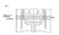
図3は、従来の最大発熱位置と実施例による最大発熱位置を示した図である。 FIG. 3 is a diagram showing a conventional maximum heat generation position and a maximum heat generation position according to the embodiment.
実施例においては、図示した通り、従来より最大発熱位置が下部に位置し、特に、最大発熱位置がMGPより100ミリメートルないし200ミリメートル下部の距離(d)に位置させることができる。この時、シリコン溶液の流れ(flow)を変化させることができ、最大発熱位置がMGPより200ミリメートル以上下部に位置すると、シリコン溶液上部の流れが乱流(turbulence)になり得、0ないし100ミリメートル下部に位置すると、シリコン溶液下部の流れが乱流になり得る。 In the embodiment, as shown in the figure, the maximum heat generation position is located lower than in the prior art, and in particular, the maximum heat generation position can be located at a distance (d) that is 100 millimeters to 200 millimeters below MGP. At this time, the flow of the silicon solution can be changed, and if the maximum heat generation position is 200 mm or more below the MGP, the flow above the silicon solution can become a turbulence, 0 to 100 mm. When located at the bottom, the flow below the silicon solution can be turbulent.
実施例においては、最大発熱位置をMGPより100ミリメートルないし200ミリメートル下部に位置させ、シリコン融液の深さ方向、すなわち図1の上下方向回への流れを一定にすることができる。 In the embodiment, the maximum heat generation position is located 100 mm to 200 mm below the MGP, and the flow of the silicon melt in the depth direction, that is, in the vertical direction of FIG. 1, can be made constant.
成長するインゴットから製造されるシリコンウェハーのハイゲッタリング(high gettering)および均一性(uniformity)向上のために、インゴット内から酸素濃度が長さ方向および半径方向に一定であることが有利である。これのために拡散境界層が成長中のシリコン融液の表面から12ミリメートル程度の深さで、約300ミリメートルの直径外部の領域に分布することができる。実施例によるシリコン単結晶インゴットの成長方法においてシリコン融液内の拡散境界層が半径方向の端部に均一に分布できるが、拡散境界層はシリコン融液の温度を測定して確認することができる。 In order to improve the high gettering and uniformity of silicon wafers produced from growing ingots, it is advantageous that the oxygen concentration is constant in the longitudinal and radial directions from within the ingot. For this purpose, the diffusion boundary layer can be distributed in a region outside the diameter of about 300 millimeters at a depth of about 12 millimeters from the surface of the growing silicon melt. In the method for growing a silicon single crystal ingot according to the embodiment, the diffusion boundary layer in the silicon melt can be uniformly distributed at the end in the radial direction, but the diffusion boundary layer can be confirmed by measuring the temperature of the silicon melt. .
このとき、前記のヒーターと引き上げ手段は、前記シリコン融液の半径方向の端部に均一に拡散境界層が分布するように前記るつぼを加熱して前記インゴットを引き上げることができる。詳細には前記ヒーターと引き上げ手段は、前記拡散境界層が前記シリコン融液の表面から12ミリメートル下部に形成されるように前記るつぼを加熱して前記インゴットを引き上げることができる。 In this case, the heater and the pulling means can pull the ingot by heating the crucible so that the diffusion boundary layer is uniformly distributed at the radial end of the silicon melt. Specifically, the heater and the pulling means can pull the ingot by heating the crucible so that the diffusion boundary layer is formed 12 mm below the surface of the silicon melt.
詳細には拡散境界層は、拡散速度が10-8m2/初程度である領域であり、本実施例において1700ケルビン(Kelvin)程度の温度で拡散境界層は最大直径が320ミリメートルであり得る。 Specifically, the diffusion boundary layer is a region having a diffusion rate of about 10 −8 m 2 / initial, and in this example, the diffusion boundary layer can have a maximum diameter of 320 millimeters at a temperature of about 1700 Kelvin. .
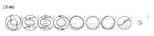
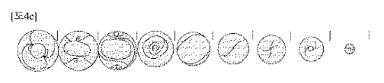
図4aないし図4cは、実施例によるシリコン単結晶インゴットの成長方法でシリコン融液の流れを比較例とともに示した図である。 4a to 4c are views showing a flow of a silicon melt together with a comparative example in a method for growing a silicon single crystal ingot according to an embodiment.
左側がシリコン融液の表面でのシリコン融液の流れであり、右側に行くほど下部領域での流れを示し、最右側はるつぼの底面でのシリコン融液の流れを示す。 The left side is the flow of the silicon melt on the surface of the silicon melt, the flow in the lower region is shown toward the right side, and the rightmost side is the flow of the silicon melt on the bottom of the crucible.
図4bと図4cの第1実施例と第2実施例、特に第1実施例によるシリコン単結晶インゴットの成長方法でシリコン融液の流れのパターンが下部領域でも維持されるが、従来技術の場合、シリコン融液の流れのパターンが下部では薄れ得る。。 4b and 4c, the flow pattern of the silicon melt is maintained in the lower region in the growth method of the silicon single crystal ingot according to the first embodiment and the second embodiment, particularly the first embodiment. The flow pattern of the silicon melt can be thinned at the bottom. .
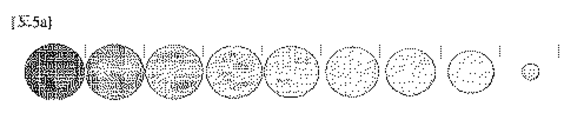
図5aないし5cは、実施例によるシリコン単結晶インゴットの成長方法でシリコン融液の酸素の分布を比較例とともに示した図である。図5bと図5cにおいて拡散境界層がインゴットの端部で維持されてシリコン融液の速度変化が抑制されて酸素濃度が深さ方向に2200ミリメートルまで均一であるが、図5aの比較例の場合、シリコン融液の流れが一定せず酸素濃度が深さ方向に2000ミリメートルで不均一であり得る。 FIGS. 5a to 5c are diagrams showing oxygen distribution in a silicon melt together with a comparative example in a method for growing a silicon single crystal ingot according to an embodiment. 5b and 5c, the diffusion boundary layer is maintained at the end of the ingot to suppress the speed change of the silicon melt and the oxygen concentration is uniform up to 2200 millimeters in the depth direction. The flow of the silicon melt may not be constant, and the oxygen concentration may be uneven at 2000 millimeters in the depth direction.
図6aは、実施例によるシリコン単結晶インゴットの成長方法において酸素濃度の均一度を示した図面であり、図6bは、比較例によるシリコン単結晶インゴットの成長方法において酸素濃度の均一度を示した図である。 FIG. 6A is a view showing the uniformity of oxygen concentration in the method for growing a silicon single crystal ingot according to the example, and FIG. 6B is the view showing uniformity of oxygen concentration in the method for growing a silicon single crystal ingot according to a comparative example. FIG.
図6aにおいて、シリコンウェハーは、直径がそれぞれ180ミリメートルと220ミリメートルであり、比抵抗がそれぞれ0.09と0.11であり、一つのインゴットから製造されたシリコンウェハーの酸素濃度が半径方向でほとんど均一である。図6dにおいてシリコンウェハーは、直径が110ミリメートルと180ミリメートルであり、比抵抗がそれぞれ0.16と0.19であり、一つのインゴットから製造されたシリコンウェハーの酸素濃度が半径方向で大きい散布を示している。 In FIG. 6a, the silicon wafer has a diameter of 180 millimeters and 220 millimeters, respectively, the specific resistances are 0.09 and 0.11, respectively, and the oxygen concentration of the silicon wafer manufactured from one ingot is almost in the radial direction. It is uniform. In FIG. 6d, the silicon wafer has a diameter of 110 millimeters and 180 millimeters, specific resistances of 0.16 and 0.19, respectively, and a silicon wafer manufactured from one ingot has a large oxygen concentration in the radial direction. Show.
したがって、前述した実施例による工程でシリコン単結晶インゴットを成長させる時、シリコン融液の流れが一定して、拡散境界層がインゴットの端部に分布して、製造されたシリコンウェハーの酸素濃度が一定し、比抵抗が改善されることがわかる。 Therefore, when the silicon single crystal ingot is grown in the process according to the above-described embodiment, the flow of the silicon melt is constant, the diffusion boundary layer is distributed at the end of the ingot, and the oxygen concentration of the manufactured silicon wafer is It can be seen that the specific resistance is improved.
以上、実施例を中心に説明したがこれは単なる例示に過ぎず、本発明を限定するものではなく、本発明が属する分野の通常の知識を有した者であれば本実施例の本質的な特性を逸脱しない範囲で、以上で例示されていない様々な変形と応用が可能であることが理解できるだろう。例えば、実施例に具体的に示された各構成要素は変形して実施することができるものである。そして、このような変形と応用に係る差異点は添付された請求範囲で規定する本発明の範囲に含まれるものと解釈されるべきである。 Although the embodiments have been described above, this is merely an example, and is not intended to limit the present invention. Any person having ordinary knowledge in the field to which the present invention belongs can be used. It will be understood that various modifications and applications not exemplified above are possible without departing from the characteristics. For example, each component specifically shown in the embodiments can be modified and implemented. Such differences in modification and application should be construed as being included in the scope of the present invention as defined in the appended claims.
[産業上利用可能性]
実施例は、シリコン単結晶インゴットの成長装置および方法は、シリコン単結晶インゴットで直径方向と半径方向の酸素濃度の均一性を向上させることができる。
[Industrial applicability]
In the embodiment, the silicon single crystal ingot growth apparatus and method can improve the uniformity of the oxygen concentration in the diameter direction and the radial direction in the silicon single crystal ingot.
実施例は、シリコン単結晶インゴットの成長装置及び方法に関するものであり、より詳細には高ドーピングシリコン単結晶インゴットにおいて直径方向と半径方向の酸素濃度の均一性を確保しようとする。 The embodiment relates to an apparatus and a method for growing a silicon single crystal ingot, and more particularly, to ensure uniformity of oxygen concentration in a diameter direction and a radial direction in a highly doped silicon single crystal ingot.
通常のシリコンウェハーは、単結晶インゴット(Ingot)を作るための単結晶成長工程と、単結晶インゴットをスライシング(Slicing)して薄い円板状のウェハーを得るスライシング工程と、前記スライシング工程によって得られたウェハーの割れ、歪みを防止するためにその外周部を加工するグラインディング(Grinding)工程と、前記ウェハーに残存する機械的加工による損傷(Damage)を除去するラッピング(Lapping)工程と、前記ウェハーを鏡面化する研磨(Polishing)工程と、研磨されたウェハーを研磨してウェハーに付着した研磨剤や異物を除去する洗浄工程とを含んで成り立つ。 A normal silicon wafer is obtained by a single crystal growth process for making a single crystal ingot, a slicing process for slicing a single crystal ingot to obtain a thin disk-shaped wafer, and the slicing process. In order to prevent cracking and distortion of the wafer, a grinding process for processing the outer periphery thereof, a lapping process for removing damage (damage) caused by mechanical processing remaining on the wafer, and the wafer The polishing process includes a polishing process for polishing the surface of the wafer and a cleaning process for polishing the polished wafer to remove abrasives and foreign substances adhering to the wafer.
単結晶成長は、フローティングゾーン(floating zone:FZ)方法またはチョクラルスキー(Czochralski:CZ、以下、CZと称する)方法を多く使用して来た。これらの方法の中で最も一般化されている方法がCZ方法である。 Single crystal growth has often used a floating zone (FZ) method or a Czochralski (CZ) method. The most generalized method among these methods is the CZ method.
CZ方法においては、石英るつぼに多結晶シリコンを装入し、これを黒煙発熱体によって加熱して溶融させた後、溶融の結果形成されたシリコン溶融液に種子結晶を浸して界面で結晶化が起きる時シードを回転しながら引き上げることによって単結晶のシリコンインゴットを成長させる。 In the CZ method, polycrystalline silicon is charged into a quartz crucible, heated and melted by a black smoke heating element, and then seed crystals are immersed in a silicon melt formed as a result of melting and crystallized at the interface. When this occurs, a single crystal silicon ingot is grown by pulling the seed up while rotating.
シリコン単結晶の成長過程で成長履歴による結晶欠陥及び望まない不純物として特に酸素がシリコン単結晶に含まれるようになる。このように陥入された酸素は半導体素子の製造工程で加えられる熱によって酸素沈殿物(oxygen precipitates)に成長するようになるが、この酸素沈殿物はシリコンウェハーの強度を補強して金属汚染元素を捕獲するなど内部ゲッタリング(Internal Gettering)サイトとして作用するなど有益な特性を示しもするが、半導体素子の漏洩電流及び不良(fail)を誘発する有害な特性を示す。 In particular, oxygen is included in the silicon single crystal as crystal defects and unwanted impurities due to the growth history during the growth process of the silicon single crystal. The invaded oxygen grows into oxygen precipitates by heat applied in the manufacturing process of the semiconductor device, and the oxygen precipitate reinforces the strength of the silicon wafer and is a metal contamination element. It exhibits beneficial characteristics such as acting as an internal gettering site such as trapping the semiconductor, but exhibits harmful characteristics that induce leakage current and failure of the semiconductor device.
したがって、シリコン単結晶インゴットから製造されたウェハーの酸素濃度を長さ方向及び半径方向で均一にする必要があり、シリコン単結晶インゴットを成長させるときの工程変数であるシード(seed)回転速度、るつぼ回転速度、融液(melt)表面と熱遮蔽材(heat shield)との間の間隔であるメルトギャップ(melt gap)、インゴットの引き上げ速度(pull speed)、ホットゾーン(hot zone)のデザイン変更、窒素や炭素などの第3の元素ドーピングなどを通じて酸素濃度を調節することができる。 Therefore, it is necessary to make the oxygen concentration of the wafer manufactured from the silicon single crystal ingot uniform in the length direction and the radial direction, and the seed rotation speed and the crucible which are process variables when growing the silicon single crystal ingot. Rotational speed, melt gap, which is the distance between the melt surface and the heat shield, a change in the pull speed of the ingot, a change in the design of the hot zone, The oxygen concentration can be adjusted through third element doping such as nitrogen and carbon.
しかし、現在、製造されたシリコン単結晶インゴットから求められたウエハーの場合、特に端部に環形で酸素濃度が不均一な領域が発見されており、前述した内部ゲッタリング特性の不均一に起因し得る。 However, at present, in the case of a wafer obtained from a manufactured silicon single crystal ingot, an annular region having a nonuniform oxygen concentration has been found particularly at the end, which is caused by the nonuniformity of the internal gettering characteristics described above. obtain.
実施例は、シリコン単結晶の成長時に長さ方向及び半径方向の酸素濃度の均一性を向上させようとする。 The embodiment attempts to improve the uniformity of the oxygen concentration in the length direction and the radial direction during the growth of the silicon single crystal.
実施例は、チャンバ;前記チャンバの内部に具備され、シリコン溶液が収容されるるつぼ;前記るつぼの下部に配置されるるつぼ支持台と回転軸;前記チャンバの内部に具備され、前記シリコン溶液を加熱するヒーター;前記シリコン溶液から成長するインゴットを回転しながら引き上げる引き上げ手段;及び前記るつぼに水平磁場を印加する磁場発生ユニットを含み、前記回転軸が前記るつぼを回転させる第1方向と前記引き上げ手段が前記インゴットを回転させる第2方向は互いに同一なシリコン単結晶インゴットの成長装置を提供する。 An embodiment includes a chamber; a crucible provided in the chamber and containing a silicon solution; a crucible support and a rotating shaft disposed in a lower part of the crucible; provided in the chamber and heating the silicon solution. A heater for rotating the ingot grown from the silicon solution while rotating; and a magnetic field generating unit for applying a horizontal magnetic field to the crucible, wherein the rotating shaft rotates the crucible in a first direction and the pulling means includes: The second direction in which the ingot is rotated provides the same silicon single crystal ingot growth apparatus.
ヒーターは、最大発熱位置がMGP(maximum gauss position)より下部に形成されるようにるつぼの周辺を加熱することができる。 The heater can heat the periphery of the crucible so that the maximum heat generation position is formed below the MGP (maximum Gauss position).
ヒーターは、最大発熱位置が前記MGPより100ないし200mm下部に形成されるようにるつぼの周辺を加熱することができる。 The heater can heat the periphery of the crucible so that the maximum heat generation position is formed 100 to 200 mm below the MGP.
ヒーターと引き上げ手段は、シリコン溶液の半径方向の端部に均一に拡散境界層が分布するように前記るつぼを加熱して前記インゴットを引き上げることができる。 The heater and the pulling means can pull up the ingot by heating the crucible so that the diffusion boundary layer is uniformly distributed at the radial end of the silicon solution.
ヒーターと引き上げ手段は、前記拡散境界層が前記シリコン溶液の表面から12ミリメートル下部に形成されるように前記るつぼを加熱し、前記インゴットを引き上げることができる。 The heater and the pulling means can heat the crucible and pull the ingot so that the diffusion boundary layer is formed 12 millimeters below the surface of the silicon solution.
ヒーターと引き上げ手段は、前記拡散境界層が前記のシリコン溶液の端部から300ミリメートル以上の直径に分布するように前記るつぼを加熱し、前記インゴットを引き上げることができる。 The heater and the pulling means can heat the crucible so that the diffusion boundary layer is distributed in a diameter of 300 millimeters or more from the end of the silicon solution, and pull the ingot.
他の実施例は、シリコン単結晶インゴットの成長方法において、インゴットとるつぼを同一の方向に回転させ、最大発熱位置をMGP(maximum gauss position)より下部に位置させるシリコン単結晶インゴットの成長方法を提供する。 Another embodiment provides a method for growing a silicon single crystal ingot in which the ingot crucible is rotated in the same direction in a method for growing a silicon single crystal ingot, and a maximum heat generation position is located below a maximum gap position (MGP). To do.
拡散境界層がシリコン溶液の半径方向の端部に均一に分布することができる。 The diffusion boundary layer can be uniformly distributed at the radial ends of the silicon solution.
拡散境界層は、前記シリコン溶液の表面から12ミリメートル下部で300ミリメートル以上の直径に分布することができる。 The diffusion boundary layer can be distributed over a diameter of 300 millimeters or more 12 millimeters below the surface of the silicon solution.
シリコン溶液内で深さ方向に前記シリコン溶液の流れが一定することができる。 The flow of the silicon solution can be constant in the depth direction in the silicon solution.
最大発熱位置を前記MGPより100ないし200ミリメートル下部に位置させることができる。 The maximum heat generation position can be located 100 to 200 millimeters below the MGP.
前述した工程でシリコン単結晶インゴットを成長させる時、シリコン溶液の流れが一定して、拡散境界層がインゴットの端部に分布して、製造されたシリコンウェハーの酸素濃度が一定して、比抵抗が改善されたことがわかる。 When growing a silicon single crystal ingot in the above-described process, the flow of the silicon solution is constant, the diffusion boundary layer is distributed at the end of the ingot, the oxygen concentration of the manufactured silicon wafer is constant, and the specific resistance It can be seen that has been improved.
以下、本発明を具体的に説明するため、実施例を挙げて説明し、発明に対する理解を助けるために添付図面を参照して詳細に説明しようとする。しかし、本発明による実施例は様々な他の形態に変形され得、本発明の範囲が下で記述する実施例に限定されるものと解釈されてはいけない。本発明の実施例は当業界で平均的な知識を有した者に本発明をより完全に説明するために提供されるものである。 DETAILED DESCRIPTION OF THE PREFERRED EMBODIMENTS Hereinafter, the present invention will be described in detail by way of examples, and detailed description will be made with reference to the accompanying drawings in order to facilitate understanding of the invention. However, the embodiments according to the present invention may be modified in various other forms, and the scope of the present invention should not be construed to be limited to the embodiments described below. Rather, these embodiments are provided so that this disclosure will be thorough and complete, and will fully convey the concept of the invention to those skilled in the art.
本発明による実施例の説明において、各elementの“上(うえ)”または“下(した)(on or under)”に形成されるものと記載される場合において、上(うえ)または下(した)(on or under)は、二つのelementが互いに直接(directly)接触したり一つ以上の他のelementが前記二つのelementの間に配置されて(indirectly)形成されるものをすべて含む。また“上(うえ)”または“下(した)(on or under)”と表現される場合、一つのelementを基準に上側方向だけでなく下側方向の意味も含むことができる。 In the description of the embodiment according to the present invention, when it is described that it is formed “on” or “on” under each element, it is above (above) or below. ) (On or under) includes all elements in which two elements are in direct contact with each other or one or more other elements are indirectly arranged between the two elements. In addition, the expression “upper” or “on or under” may include not only the upper direction but also the meaning of the lower direction on the basis of one element.
また、以下で用いられる“第1”及び“第2”、“上部”及び“下部”などのような関係的用語は、その実体または要素などの間のどんな物理的または論理的関係または手順を必ず要求したり内包したりせず、ある一の実体または要素を他の実体または要素と区別するためにのみ利用され得る。 Also, relational terms such as “first” and “second”, “upper” and “lower” used below refer to any physical or logical relationship or procedure between its entities or elements etc. It does not necessarily require or contain and can only be used to distinguish one entity or element from another.
図面において、各層の厚さや大きさは説明の便宜及び明確性のために誇張されたり省略されたりまたは概略的に図示された。また各構成要素の大きさは実際の大きさを全面的に反映したものではない。 In the drawings, the thickness and size of each layer are exaggerated, omitted, or schematically illustrated for convenience of explanation and clarity. Also, the size of each component does not fully reflect the actual size.
図1は、実施例による単結晶インゴット製造装置を示した図である。 FIG. 1 is a diagram illustrating a single crystal ingot manufacturing apparatus according to an embodiment.
実施例によるシリコン単結晶インゴット製造装置(100)はチャンバー(110)、るつぼ(120)、ヒーター(130)、引き上げ手段(150)などを含むことができる。詳しくは、実施例によるシリコン単結晶インゴット製造装置(100)は、チャンバー(110)と、前記チャンバー(110)の内部に具備され、シリコン溶液を収容するるつぼ(120)と、前記チャンバー(110)の内部に具備され、前記るつぼ(120)を加熱するヒーター(130)及び種子結晶(152)が一端に結合された引き上げ手段(150)とるつぼ(120)に水平磁場を印加する磁場発生ユニット(図示せず)を含むことができる。 The apparatus for manufacturing a silicon single crystal ingot (100) according to the embodiment may include a chamber (110), a crucible (120), a heater (130), a pulling means (150), and the like. Specifically, a silicon single crystal ingot manufacturing apparatus (100) according to an embodiment includes a chamber (110), a crucible (120) that is provided in the chamber (110), and stores a silicon solution, and the chamber (110). A heating unit (130) for heating the crucible (120) and a lifting means (150) coupled to one end of the seed crystal (152), and a magnetic field generating unit for applying a horizontal magnetic field to the crucible (120). (Not shown).
チャンバ(110)は、半導体などの電子部品素材として使用されるシリコンウェハー(wafer)用の単結晶インゴット(ingot)を成長させるための所定の工程が遂行される空間を提供する。
The
チャンバ(110)の内壁においては、ヒーター(130)の熱が前記チャンバ(110)の側壁部に放出されないように輻射断熱体(140)が設置され得る。 A radiation insulator (140) may be installed on the inner wall of the chamber (110) so that heat of the heater (130) is not released to the side wall of the chamber (110).
シリコン単結晶成長時の酸素濃度を制御するために るつぼ(120)の回転速度やチャンバ(110)内部の圧力条件など多様な因子を調節することができる。例えば、実施例は酸素濃度を制御するためにシリコン単結晶成長装置のチャンバ(110)内部にアルゴンガスなどを注入して下部に排出することができる。 In order to control the oxygen concentration during the growth of the silicon single crystal, various factors such as the rotational speed of the crucible (120) and the pressure conditions inside the chamber (110) can be adjusted. For example, in the embodiment, argon gas or the like can be injected into the chamber (110) of the silicon single crystal growth apparatus and discharged below to control the oxygen concentration.
前記るつぼ(120)は、シリコン溶融液を収容することができるように前記チャンバ(110)の内部に具備され、石英などからなることができる。前記るつぼ(120)の外部にはるつぼ(120)を支持することができるように黒煙からなるるつぼ支持台(図示せず)が具備され得る。前記るつぼ支持台は、回転軸(図示せず)上に固定設置され、前記回転軸は、駆動手段(図示せず)によって回転されてるつぼ(120)を回転及び昇降運動させながら固−液界面、すなわち、固化されたインゴットとシリコン溶液の境界面が同一な高さを維持するようにできる。 The crucible (120) is provided in the chamber (110) so as to accommodate a silicon melt, and may be made of quartz or the like. A crucible support base (not shown) made of black smoke may be provided outside the crucible (120) to support the crucible (120). The crucible support base is fixedly installed on a rotating shaft (not shown), and the rotating shaft rotates and moves up and down a crucible (120) rotated by a driving means (not shown). That is, the interface between the solidified ingot and the silicon solution can be maintained at the same height.
また、前記回転軸は、前記るつぼを回転させる第1方向に回転させ、前記引き上げ手段が前記インゴットを回転させる第2方向に回転させることができるが、第1方向と第2方向は互いに同一とすることができる。 The rotating shaft may be rotated in a first direction for rotating the crucible, and the lifting means may be rotated in a second direction for rotating the ingot. The first direction and the second direction are the same. can do.
ヒーター(130)は、るつぼ(120)を加熱するようにチャンバ(110)の内部に具備され得、例えば、前記ヒーター(130)は、るつぼ支持台を囲む円筒状に成り立つことができる。このようなヒーター(130)は、るつぼ(120)内に積載した高純度の多結晶シリコンの塊を溶融してシリコン溶液にするようになる。 The heater (130) may be provided inside the chamber (110) to heat the crucible (120). For example, the heater (130) may have a cylindrical shape surrounding the crucible support. Such a heater (130) melts a lump of high-purity polycrystalline silicon loaded in the crucible (120) into a silicon solution.
ヒーター(130)は、供給される熱によってるつぼ(120)が加熱されるが、るつぼ(120)の高さによる領域ごとに温度が異なる場合があり得、温度が最も高い領域はヒーター(130)の最大発熱位置と対応することができる。 In the heater (130), the crucible (120) is heated by the supplied heat, but the temperature may be different for each region depending on the height of the crucible (120), and the region with the highest temperature is the heater (130). It can correspond to the maximum heat generation position.
実施例による、シリコン単結晶インゴット成長のための製造方法としては、単結晶である種子結晶(seed crystal、152)をシリコン溶液に浸した後ゆっくり引き上げながら結晶を成長させるチョクラルスキー(Czochralsk:CZ)法を採用することができる。 As a manufacturing method for growing a silicon single crystal ingot according to an embodiment, a seed crystal (seed crystal, 152), which is a single crystal, is immersed in a silicon solution, and then the crystal is grown while being slowly pulled up (Czochralsk: CZ). ) Method can be adopted.
チョクラルスキー法を詳しく説明すれば下のとおりである。 The details of the Czochralski method are as follows.
種子結晶(152)から細くて長い結晶を成長させるネッキング(necking)工程を経ると、結晶を直径方向に成長させて目標直径に作るショルダーリング(shouldering)工程を経て、以後には一定な直径を有する結晶に成長させるボディーグロイング(body growing)工程を経て、一定な長さだけボディーグロイングが進行された後には結晶の直径を徐徐に減少させて結局溶融シリコンと分離するテーリング(tailing)工程を経て単結晶成長が仕上げられる。 After passing through a necking process for growing a thin and long crystal from the seed crystal (152), a shouldering process for growing the crystal in the diameter direction to produce a target diameter is performed. A tailing process in which the diameter of the crystal is gradually reduced after the body growing is progressed by a certain length through a body growing process for growing the crystal to have a crystal, and eventually separated from the molten silicon. After that, the single crystal growth is finished.
本実施例においては、シリコン溶液にはP−タイプのドーパントとしてB(ボロン)が、N−タイプのドーパントとしてAs(砒素)、P(リン)、Sb(アンチモン)などがドーピングされ得る。高濃度のドーパントが投入される場合、ドーパントの濃度によってV/G(growth rate/temperature gradient)すなわち、温度勾配に対するインゴットの成長速度が変化することができ、これによってインゴットの内部、特にボディー(body)領域内で酸素濃度が変化することができる。 In this embodiment, the silicon solution may be doped with B (boron) as a P-type dopant and As (arsenic), P (phosphorus), Sb (antimony), or the like as an N-type dopant. When a high concentration of dopant is introduced, the growth rate of the ingot with respect to the growth rate / temperature gradient (V / G), that is, the temperature gradient can be changed according to the concentration of the dopant, and thereby the inside of the ingot, particularly the body (body). ) The oxygen concentration can vary within the region.
本実施例においては、インゴットの成長時にインゴットとるつぼを同一の方向に回転させ、最大発熱位置がMGP(maximum gauss position)より下部に位置するようにヒーターを配置し、インゴットの長さ方向と半径方向(面内方向)からの酸素濃度を一定にして生産されるウエハーの比抵抗を一定にすることができる。 In this embodiment, when the ingot is grown, the crucible for the ingot is rotated in the same direction, the heater is arranged so that the maximum heat generation position is located below the MGP (maximum Gauss position), the length direction and radius of the ingot The specific resistance of the wafer to be produced can be made constant by keeping the oxygen concentration from the direction (in-plane direction) constant.
詳細には、前記磁場印加ユニットによってるつぼ(120)の周辺に磁場が印加されるが、磁場の強さが最も強い領域をMGP(maximum gauss position)と言うことができる。この時、ヒーターと磁場は最大発熱位置がMGP(maximum gauss position)より下部に形成されるように前記るつぼ(120)の周辺を加熱してるつぼの周辺に磁場を印加することができ、詳細には最大発熱位置が前記MGPより100ないし200ミリメートル下部に形成されるようにすることができる。 Specifically, a magnetic field is applied to the periphery of the crucible (120) by the magnetic field application unit, and a region where the strength of the magnetic field is the strongest can be called MGP (maximum Gauss position). At this time, the heater and the magnetic field can heat the periphery of the crucible (120) so that the maximum heat generation position is formed below the MGP (maximum Gauss position), and the magnetic field can be applied to the periphery of the crucible in detail. The maximum heat generation position may be formed 100 to 200 millimeters below the MGP.
図2は、シリコン単結晶インゴットの成長時に最大ガウス地点(Maximum gauss position)の移動を示した図である。 FIG. 2 is a diagram showing the movement of the maximum gauss point when a silicon single crystal ingot is grown.
図2において、最大ガウス地点(MGP)は、るつぼ内部の領域である“A”や上部チャンバーの領域である“B”の境界面の上下に移動することができるが、MGPは前述した境界から“A”方向に“a”そして、“B”方向に“b”の範囲内で移動できるが、そのとき、ヒーターの最大発熱位置は前述したMGPより下部に位置することができる。 In FIG. 2, the maximum Gaussian point (MGP) can be moved up and down the boundary surface of “A”, which is the region inside the crucible, and “B”, which is the region of the upper chamber. The heater can move within the range of “a” in the “A” direction and “b” in the “B” direction. At this time, the maximum heat generation position of the heater can be located below the above-described MGP.
図3は、従来の最大発熱位置と実施例による最大発熱位置を示した図である。 FIG. 3 is a diagram showing a conventional maximum heat generation position and a maximum heat generation position according to the embodiment.
実施例においては、図示した通り、従来より最大発熱位置が下部に位置し、特に、最大発熱位置がMGPより100ミリメートルないし200ミリメートル下部の距離(d)に位置させることができる。この時、シリコン溶液の流れ(flow)を変化させることができ、最大発熱位置がMGPより200ミリメートル以上下部に位置すると、シリコン溶液上部の流れが乱流(turbulence)になり得、0ないし100ミリメートル下部に位置すると、シリコン溶液下部の流れが乱流になり得る。 In the embodiment, as shown in the figure, the maximum heat generation position is located lower than in the prior art, and in particular, the maximum heat generation position can be located at a distance (d) that is 100 millimeters to 200 millimeters below MGP. At this time, the flow of the silicon solution can be changed, and if the maximum heat generation position is 200 mm or more below the MGP, the flow above the silicon solution can become a turbulence, 0 to 100 mm. When located at the bottom, the flow below the silicon solution can be turbulent.
実施例においては、最大発熱位置をMGPより100ミリメートルないし200ミリメートル下部に位置させ、シリコン融液の深さ方向、すなわち図1の上下方向回への流れを一定にすることができる。 In the embodiment, the maximum heat generation position is located 100 mm to 200 mm below the MGP, and the flow of the silicon melt in the depth direction, that is, in the vertical direction of FIG. 1, can be made constant.
成長するインゴットから製造されるシリコンウェハーのハイゲッタリング(high gettering)および均一性(uniformity)向上のために、インゴット内から酸素濃度が長さ方向および半径方向に一定であることが有利である。これのために拡散境界層が成長中のシリコン融液の表面から12ミリメートル程度の深さで、約300ミリメートルの直径外部の領域に分布することができる。実施例によるシリコン単結晶インゴットの成長方法においてシリコン融液内の拡散境界層が半径方向の端部に均一に分布できるが、拡散境界層はシリコン融液の温度を測定して確認することができる。 In order to improve the high gettering and uniformity of silicon wafers produced from growing ingots, it is advantageous that the oxygen concentration is constant in the longitudinal and radial directions from within the ingot. For this purpose, the diffusion boundary layer can be distributed in a region outside the diameter of about 300 millimeters at a depth of about 12 millimeters from the surface of the growing silicon melt. In the method for growing a silicon single crystal ingot according to the embodiment, the diffusion boundary layer in the silicon melt can be uniformly distributed at the end in the radial direction, but the diffusion boundary layer can be confirmed by measuring the temperature of the silicon melt. .
このとき、前記のヒーターと引き上げ手段は、前記シリコン融液の半径方向の端部に均一に拡散境界層が分布するように前記るつぼを加熱して前記インゴットを引き上げることができる。詳細には前記ヒーターと引き上げ手段は、前記拡散境界層が前記シリコン融液の表面から12ミリメートル下部に形成されるように前記るつぼを加熱して前記インゴットを引き上げることができる。 In this case, the heater and the pulling means can pull the ingot by heating the crucible so that the diffusion boundary layer is uniformly distributed at the radial end of the silicon melt. Specifically, the heater and the pulling means can pull the ingot by heating the crucible so that the diffusion boundary layer is formed 12 mm below the surface of the silicon melt.
詳細には拡散境界層は、拡散速度が10-8m2/初程度である領域であり、本実施例において1700ケルビン(Kelvin)程度の温度で拡散境界層は最大直径が320ミリメートルであり得る。 Specifically, the diffusion boundary layer is a region having a diffusion rate of about 10 −8 m 2 / initial, and in this example, the diffusion boundary layer can have a maximum diameter of 320 millimeters at a temperature of about 1700 Kelvin. .
図4aないし図4cは、実施例によるシリコン単結晶インゴットの成長方法でシリコン融液の流れを比較例とともに示した図である。 4a to 4c are views showing a flow of a silicon melt together with a comparative example in a method for growing a silicon single crystal ingot according to an embodiment.
左側がシリコン融液の表面でのシリコン融液の流れであり、右側に行くほど下部領域での流れを示し、最右側はるつぼの底面でのシリコン融液の流れを示す。 The left side is the flow of the silicon melt on the surface of the silicon melt, the flow in the lower region is shown toward the right side, and the rightmost side is the flow of the silicon melt on the bottom of the crucible.
図4bと図4cの第1実施例と第2実施例、特に第1実施例によるシリコン単結晶インゴットの成長方法でシリコン融液の流れのパターンが下部領域でも維持されるが、従来技術の場合、シリコン融液の流れのパターンが下部では薄れ得る。。 4b and 4c, the flow pattern of the silicon melt is maintained in the lower region in the growth method of the silicon single crystal ingot according to the first embodiment and the second embodiment, particularly the first embodiment. The flow pattern of the silicon melt can be thinned at the bottom. .
図5aないし5cは、実施例によるシリコン単結晶インゴットの成長方法でシリコン融液の酸素の分布を比較例とともに示した図である。図5bと図5cにおいて拡散境界層がインゴットの端部で維持されてシリコン融液の速度変化が抑制されて酸素濃度が深さ方向に2200ミリメートルまで均一であるが、図5aの比較例の場合、シリコン融液の流れが一定せず酸素濃度が深さ方向に2000ミリメートルで不均一であり得る。 FIGS. 5a to 5c are diagrams showing oxygen distribution in a silicon melt together with a comparative example in a method for growing a silicon single crystal ingot according to an embodiment. 5b and 5c, the diffusion boundary layer is maintained at the end of the ingot to suppress the speed change of the silicon melt and the oxygen concentration is uniform up to 2200 millimeters in the depth direction. The flow of the silicon melt may not be constant, and the oxygen concentration may be uneven at 2000 millimeters in the depth direction.
図6aは、実施例によるシリコン単結晶インゴットの成長方法において酸素濃度の均一度を示した図面であり、図6bは、比較例によるシリコン単結晶インゴットの成長方法において酸素濃度の均一度を示した図である。 FIG. 6A is a view showing the uniformity of oxygen concentration in the method for growing a silicon single crystal ingot according to the example, and FIG. 6B is the view showing uniformity of oxygen concentration in the method for growing a silicon single crystal ingot according to a comparative example. FIG.
図6aにおいて、シリコンウェハーは、直径がそれぞれ1800ミリメートルと2200ミリメートルであり、比抵抗がそれぞれ0.09と0.11であり、一つのインゴットから製造されたシリコンウェハーの酸素濃度が半径方向でほとんど均一である。図6bにおいてシリコンウェハーは、直径が1100ミリメートルと1800ミリメートルであり、比抵抗がそれぞれ0.16と0.19であり、一つのインゴットから製造されたシリコンウェハーの酸素濃度が半径方向で大きい散布を示している。 In FIG. 6a, the silicon wafer has a diameter of 1800 millimeters and 2200 millimeters, respectively, specific resistances of 0.09 and 0.11, respectively, and the oxygen concentration of a silicon wafer manufactured from one ingot is almost in the radial direction. It is uniform. In FIG. 6b, the silicon wafer has a diameter of 1100 millimeters and 1800 millimeters, specific resistances of 0.16 and 0.19, respectively, and a silicon wafer manufactured from one ingot has a large oxygen concentration in the radial direction. Show.
したがって、前述した実施例による工程でシリコン単結晶インゴットを成長させる時、シリコン融液の流れが一定して、拡散境界層がインゴットの端部に分布して、製造されたシリコンウェハーの酸素濃度が一定し、比抵抗が改善されることがわかる。 Therefore, when the silicon single crystal ingot is grown in the process according to the above-described embodiment, the flow of the silicon melt is constant, the diffusion boundary layer is distributed at the end of the ingot, and the oxygen concentration of the manufactured silicon wafer is It can be seen that the specific resistance is improved.
以上、実施例を中心に説明したがこれは単なる例示に過ぎず、本発明を限定するものではなく、本発明が属する分野の通常の知識を有した者であれば本実施例の本質的な特性を逸脱しない範囲で、以上で例示されていない様々な変形と応用が可能であることが理解できるだろう。例えば、実施例に具体的に示された各構成要素は変形して実施することができるものである。そして、このような変形と応用に係る差異点は添付された請求範囲で規定する本発明の範囲に含まれるものと解釈されるべきである。 Although the embodiments have been described above, this is merely an example, and is not intended to limit the present invention. Any person having ordinary knowledge in the field to which the present invention belongs can be used. It will be understood that various modifications and applications not exemplified above are possible without departing from the characteristics. For example, each component specifically shown in the embodiments can be modified and implemented. Such differences in modification and application should be construed as being included in the scope of the present invention as defined in the appended claims.
[産業上利用可能性]
実施例は、シリコン単結晶インゴットの成長装置および方法は、シリコン単結晶インゴットで直径方向と半径方向の酸素濃度の均一性を向上させることができる。
[Industrial applicability]
In the embodiment, the silicon single crystal ingot growth apparatus and method can improve the uniformity of the oxygen concentration in the diameter direction and the radial direction in the silicon single crystal ingot.
Claims (11)
前記チャンバの内部に具備され、シリコン融液が収容されるるつぼ;
前記るつぼの下部に配置されるるつぼ支持台と回転軸;
前記チャンバの内部に具備され、前記シリコン融液を加熱するヒーター;
前記シリコン融液から成長するインゴットを回転しながら引き上げる引き上げ手段;および
前記るつぼに水平磁場を印加する磁場発生ユニットを含み、
前記回転軸が前記るつぼを回転させる第1方向と前記引き上げ手段が前記インゴットを回転させる第2方向は互いに同一なシリコン単結晶インゴットの成長装置。 Chamber;
A crucible provided inside the chamber and containing a silicon melt;
A crucible support and a rotating shaft disposed at a lower portion of the crucible;
A heater provided in the chamber for heating the silicon melt;
A pulling means for pulling up an ingot grown from the silicon melt while rotating; and a magnetic field generating unit for applying a horizontal magnetic field to the crucible,
An apparatus for growing a silicon single crystal ingot, wherein a first direction in which the rotating shaft rotates the crucible and a second direction in which the pulling means rotates the ingot are the same.
インゴットとるつぼを同一の方向に回転させ、最大発熱位置をMGP(maximum gauss position)より下部に位置させるシリコン単結晶インゴットの成長方法。 In the method for growing a silicon single crystal ingot,
A method for growing a silicon single crystal ingot, wherein an ingot crucible is rotated in the same direction, and a maximum heat generation position is located below MGP (maximum Gauss position).
The apparatus for growing a silicon single crystal ingot according to claim 7, wherein the maximum heat generation position is positioned 100 to 200 millimeters below the MGP.
Applications Claiming Priority (3)
| Application Number | Priority Date | Filing Date | Title |
|---|---|---|---|
| KR10-2015-0052307 | 2015-04-14 | ||
| KR1020150052307A KR101729515B1 (en) | 2015-04-14 | 2015-04-14 | Method for growing silicon single crystal ingot |
| PCT/KR2016/003841 WO2016167542A1 (en) | 2015-04-14 | 2016-04-12 | Apparatus and method for growing single crystal silicon ingot |
Publications (2)
| Publication Number | Publication Date |
|---|---|
| JP2018510839A true JP2018510839A (en) | 2018-04-19 |
| JP2018510839A5 JP2018510839A5 (en) | 2019-01-31 |
Family
ID=57127285
Family Applications (1)
| Application Number | Title | Priority Date | Filing Date |
|---|---|---|---|
| JP2018504631A Pending JP2018510839A (en) | 2015-04-14 | 2016-04-12 | Silicon single crystal ingot growth apparatus and method |
Country Status (4)
| Country | Link |
|---|---|
| US (1) | US10344395B2 (en) |
| JP (1) | JP2018510839A (en) |
| KR (1) | KR101729515B1 (en) |
| WO (1) | WO2016167542A1 (en) |
Families Citing this family (2)
| Publication number | Priority date | Publication date | Assignee | Title |
|---|---|---|---|---|
| JP7342845B2 (en) * | 2020-11-25 | 2023-09-12 | 株式会社Sumco | Manufacturing method of silicon single crystal |
| CN117364225B (en) * | 2023-12-07 | 2024-02-23 | 天通控股股份有限公司 | Crystal growing method by co-rotating crystal and crucible |
Citations (10)
| Publication number | Priority date | Publication date | Assignee | Title |
|---|---|---|---|---|
| JPH08231294A (en) * | 1995-02-24 | 1996-09-10 | Toshiba Ceramics Co Ltd | Method for pulling up silicon single crystal under horizontal magnetic field |
| JPH09208385A (en) * | 1996-01-30 | 1997-08-12 | Mitsubishi Materials Corp | Growth of silicone single crystal and device therefor |
| JP2003321297A (en) * | 2002-04-25 | 2003-11-11 | Shin Etsu Handotai Co Ltd | Method for producing silicon single crystal and silicon single crystal wafer |
| JP2005015314A (en) * | 2003-06-27 | 2005-01-20 | Shin Etsu Handotai Co Ltd | Method for manufacturing single crystal, and single crystal |
| JP2007084417A (en) * | 2005-09-21 | 2007-04-05 | Siltron Inc | Apparatus for growing high quality silicon single crystal ingot and growing method using the apparatus |
| JP2008019129A (en) * | 2006-07-13 | 2008-01-31 | Sumco Corp | Apparatus for producing single crystal, method for producing single crystal, and single crystal |
| JP2008214118A (en) * | 2007-03-01 | 2008-09-18 | Shin Etsu Handotai Co Ltd | Method for manufacturing semiconductor single crystal |
| JP2010024120A (en) * | 2008-07-24 | 2010-02-04 | Sumco Corp | Silicon single crystal and its growing method |
| WO2013176396A1 (en) * | 2012-05-23 | 2013-11-28 | 주식회사 엘지실트론 | Single crystal silicon ingot and wafer, and apparatus and method for growing said ingot |
| JP2014214067A (en) * | 2013-04-26 | 2014-11-17 | 信越半導体株式会社 | Production method of silicon single crystal |
Family Cites Families (7)
| Publication number | Priority date | Publication date | Assignee | Title |
|---|---|---|---|---|
| JP2546736B2 (en) * | 1990-06-21 | 1996-10-23 | 信越半導体株式会社 | Silicon single crystal pulling method |
| JP2940437B2 (en) | 1995-06-01 | 1999-08-25 | 信越半導体株式会社 | Method and apparatus for producing single crystal |
| JP4853237B2 (en) * | 2006-11-06 | 2012-01-11 | 株式会社Sumco | Epitaxial wafer manufacturing method |
| KR100954291B1 (en) * | 2008-01-21 | 2010-04-26 | 주식회사 실트론 | Apparatus for manufacturing high-quality semiconductor single crystal ingot and Method using the same |
| KR101105475B1 (en) * | 2009-02-04 | 2012-01-13 | 주식회사 엘지실트론 | Method for manufacturing single crystal minimizing process-deviation |
| KR101379798B1 (en) * | 2012-05-23 | 2014-04-01 | 주식회사 엘지실트론 | Apparatus and method for growing monocrystalline silicon ingots |
| KR20150007885A (en) * | 2013-07-12 | 2015-01-21 | 엘지이노텍 주식회사 | Phosphor and light emitting device having thereof |
-
2015
- 2015-04-14 KR KR1020150052307A patent/KR101729515B1/en active IP Right Grant
-
2016
- 2016-04-12 US US15/564,045 patent/US10344395B2/en active Active
- 2016-04-12 WO PCT/KR2016/003841 patent/WO2016167542A1/en active Application Filing
- 2016-04-12 JP JP2018504631A patent/JP2018510839A/en active Pending
Patent Citations (10)
| Publication number | Priority date | Publication date | Assignee | Title |
|---|---|---|---|---|
| JPH08231294A (en) * | 1995-02-24 | 1996-09-10 | Toshiba Ceramics Co Ltd | Method for pulling up silicon single crystal under horizontal magnetic field |
| JPH09208385A (en) * | 1996-01-30 | 1997-08-12 | Mitsubishi Materials Corp | Growth of silicone single crystal and device therefor |
| JP2003321297A (en) * | 2002-04-25 | 2003-11-11 | Shin Etsu Handotai Co Ltd | Method for producing silicon single crystal and silicon single crystal wafer |
| JP2005015314A (en) * | 2003-06-27 | 2005-01-20 | Shin Etsu Handotai Co Ltd | Method for manufacturing single crystal, and single crystal |
| JP2007084417A (en) * | 2005-09-21 | 2007-04-05 | Siltron Inc | Apparatus for growing high quality silicon single crystal ingot and growing method using the apparatus |
| JP2008019129A (en) * | 2006-07-13 | 2008-01-31 | Sumco Corp | Apparatus for producing single crystal, method for producing single crystal, and single crystal |
| JP2008214118A (en) * | 2007-03-01 | 2008-09-18 | Shin Etsu Handotai Co Ltd | Method for manufacturing semiconductor single crystal |
| JP2010024120A (en) * | 2008-07-24 | 2010-02-04 | Sumco Corp | Silicon single crystal and its growing method |
| WO2013176396A1 (en) * | 2012-05-23 | 2013-11-28 | 주식회사 엘지실트론 | Single crystal silicon ingot and wafer, and apparatus and method for growing said ingot |
| JP2014214067A (en) * | 2013-04-26 | 2014-11-17 | 信越半導体株式会社 | Production method of silicon single crystal |
Also Published As
| Publication number | Publication date |
|---|---|
| US10344395B2 (en) | 2019-07-09 |
| WO2016167542A1 (en) | 2016-10-20 |
| US20180094359A1 (en) | 2018-04-05 |
| KR101729515B1 (en) | 2017-04-24 |
| KR20160122453A (en) | 2016-10-24 |
Similar Documents
| Publication | Publication Date | Title |
|---|---|---|
| JP6467056B2 (en) | Silicon single crystal ingot growth equipment | |
| JP2014509584A (en) | Method for producing single crystal ingot and single crystal ingot and wafer produced thereby | |
| CN108779577B (en) | Method for producing silicon single crystal | |
| JP5283543B2 (en) | Method for growing silicon single crystal | |
| KR101841550B1 (en) | Apparatus and method for growing silicon single crystal ingot | |
| JP2010202414A (en) | Method for growing silicon single crystal and method for producing silicon wafer | |
| JP4193610B2 (en) | Single crystal manufacturing method | |
| JP2018510839A (en) | Silicon single crystal ingot growth apparatus and method | |
| KR101942322B1 (en) | An apparatus for growing a crystal ingot and a method for growing a crystal ingot using the same | |
| JP2008189485A (en) | Method and apparatus for manufacturing silicon single crystal | |
| KR20170088120A (en) | Single crystal ingot growth apparatus and the growing method of it | |
| JP4484540B2 (en) | Manufacturing method of single crystal semiconductor | |
| JP2004315258A (en) | Production method for single crystal | |
| JP6107308B2 (en) | Silicon single crystal manufacturing method | |
| JP5668786B2 (en) | Method for growing silicon single crystal and method for producing silicon wafer | |
| JP2018510839A5 (en) | ||
| JP6958632B2 (en) | Silicon single crystal and its manufacturing method and silicon wafer | |
| JP5617812B2 (en) | Silicon single crystal wafer, epitaxial wafer, and manufacturing method thereof | |
| JP2007103877A (en) | SEMI-INSULATED GaAs WAFER MANUFACTURING METHOD | |
| JP2007210820A (en) | Method of manufacturing silicon single crystal | |
| JP2009292684A (en) | Silicon single crystal production method and production apparatus therefore | |
| KR101741101B1 (en) | Silicon single crystal ingot and method for manufacturing the same | |
| JP4150167B2 (en) | Method for producing silicon single crystal | |
| TWI832759B (en) | Method for growing silicon single crystal, method for manufacturing silicon wafer and single crystal pulling device | |
| KR101625431B1 (en) | Method for growing a silicon single crystal using czochralski method and silicon single crystal ingot |
Legal Events
| Date | Code | Title | Description |
|---|---|---|---|
| A521 | Request for written amendment filed |
Free format text: JAPANESE INTERMEDIATE CODE: A523 Effective date: 20171010 |
|
| A621 | Written request for application examination |
Free format text: JAPANESE INTERMEDIATE CODE: A621 Effective date: 20171010 |
|
| A977 | Report on retrieval |
Free format text: JAPANESE INTERMEDIATE CODE: A971007 Effective date: 20180625 |
|
| A131 | Notification of reasons for refusal |
Free format text: JAPANESE INTERMEDIATE CODE: A131 Effective date: 20180710 |
|
| A601 | Written request for extension of time |
Free format text: JAPANESE INTERMEDIATE CODE: A601 Effective date: 20181010 |
|
| A524 | Written submission of copy of amendment under article 19 pct |
Free format text: JAPANESE INTERMEDIATE CODE: A524 Effective date: 20181210 |
|
| A131 | Notification of reasons for refusal |
Free format text: JAPANESE INTERMEDIATE CODE: A131 Effective date: 20190305 |
|
| A02 | Decision of refusal |
Free format text: JAPANESE INTERMEDIATE CODE: A02 Effective date: 20191015 |