JP2018501644A - Porous interconnected corrugated carbon based network (ICCN) composites - Google Patents
Porous interconnected corrugated carbon based network (ICCN) composites Download PDFInfo
- Publication number
- JP2018501644A JP2018501644A JP2017526533A JP2017526533A JP2018501644A JP 2018501644 A JP2018501644 A JP 2018501644A JP 2017526533 A JP2017526533 A JP 2017526533A JP 2017526533 A JP2017526533 A JP 2017526533A JP 2018501644 A JP2018501644 A JP 2018501644A
- Authority
- JP
- Japan
- Prior art keywords
- composite material
- porous iccn
- porous
- metal nanoparticles
- iccn composite
- Prior art date
- Legal status (The legal status is an assumption and is not a legal conclusion. Google has not performed a legal analysis and makes no representation as to the accuracy of the status listed.)
- Pending
Links
Images


Classifications
-
- H—ELECTRICITY
- H01—ELECTRIC ELEMENTS
- H01G—CAPACITORS; CAPACITORS, RECTIFIERS, DETECTORS, SWITCHING DEVICES OR LIGHT-SENSITIVE DEVICES, OF THE ELECTROLYTIC TYPE
- H01G11/00—Hybrid capacitors, i.e. capacitors having different positive and negative electrodes; Electric double-layer [EDL] capacitors; Processes for the manufacture thereof or of parts thereof
- H01G11/22—Electrodes
- H01G11/30—Electrodes characterised by their material
- H01G11/32—Carbon-based
- H01G11/36—Nanostructures, e.g. nanofibres, nanotubes or fullerenes
-
- C—CHEMISTRY; METALLURGY
- C01—INORGANIC CHEMISTRY
- C01B—NON-METALLIC ELEMENTS; COMPOUNDS THEREOF; METALLOIDS OR COMPOUNDS THEREOF NOT COVERED BY SUBCLASS C01C
- C01B32/00—Carbon; Compounds thereof
- C01B32/15—Nano-sized carbon materials
- C01B32/182—Graphene
- C01B32/184—Preparation
-
- C—CHEMISTRY; METALLURGY
- C01—INORGANIC CHEMISTRY
- C01B—NON-METALLIC ELEMENTS; COMPOUNDS THEREOF; METALLOIDS OR COMPOUNDS THEREOF NOT COVERED BY SUBCLASS C01C
- C01B32/00—Carbon; Compounds thereof
- C01B32/15—Nano-sized carbon materials
- C01B32/182—Graphene
- C01B32/194—After-treatment
-
- C—CHEMISTRY; METALLURGY
- C25—ELECTROLYTIC OR ELECTROPHORETIC PROCESSES; APPARATUS THEREFOR
- C25D—PROCESSES FOR THE ELECTROLYTIC OR ELECTROPHORETIC PRODUCTION OF COATINGS; ELECTROFORMING; APPARATUS THEREFOR
- C25D15/00—Electrolytic or electrophoretic production of coatings containing embedded materials, e.g. particles, whiskers, wires
-
- C—CHEMISTRY; METALLURGY
- C25—ELECTROLYTIC OR ELECTROPHORETIC PROCESSES; APPARATUS THEREFOR
- C25D—PROCESSES FOR THE ELECTROLYTIC OR ELECTROPHORETIC PRODUCTION OF COATINGS; ELECTROFORMING; APPARATUS THEREFOR
- C25D9/00—Electrolytic coating other than with metals
- C25D9/04—Electrolytic coating other than with metals with inorganic materials
- C25D9/08—Electrolytic coating other than with metals with inorganic materials by cathodic processes
-
- H—ELECTRICITY
- H01—ELECTRIC ELEMENTS
- H01G—CAPACITORS; CAPACITORS, RECTIFIERS, DETECTORS, SWITCHING DEVICES OR LIGHT-SENSITIVE DEVICES, OF THE ELECTROLYTIC TYPE
- H01G11/00—Hybrid capacitors, i.e. capacitors having different positive and negative electrodes; Electric double-layer [EDL] capacitors; Processes for the manufacture thereof or of parts thereof
- H01G11/02—Hybrid capacitors, i.e. capacitors having different positive and negative electrodes; Electric double-layer [EDL] capacitors; Processes for the manufacture thereof or of parts thereof using combined reduction-oxidation reactions, e.g. redox arrangement or solion
-
- H—ELECTRICITY
- H01—ELECTRIC ELEMENTS
- H01G—CAPACITORS; CAPACITORS, RECTIFIERS, DETECTORS, SWITCHING DEVICES OR LIGHT-SENSITIVE DEVICES, OF THE ELECTROLYTIC TYPE
- H01G11/00—Hybrid capacitors, i.e. capacitors having different positive and negative electrodes; Electric double-layer [EDL] capacitors; Processes for the manufacture thereof or of parts thereof
- H01G11/22—Electrodes
- H01G11/26—Electrodes characterised by their structure, e.g. multi-layered, porosity or surface features
-
- H—ELECTRICITY
- H01—ELECTRIC ELEMENTS
- H01G—CAPACITORS; CAPACITORS, RECTIFIERS, DETECTORS, SWITCHING DEVICES OR LIGHT-SENSITIVE DEVICES, OF THE ELECTROLYTIC TYPE
- H01G11/00—Hybrid capacitors, i.e. capacitors having different positive and negative electrodes; Electric double-layer [EDL] capacitors; Processes for the manufacture thereof or of parts thereof
- H01G11/22—Electrodes
- H01G11/30—Electrodes characterised by their material
- H01G11/46—Metal oxides
-
- H—ELECTRICITY
- H01—ELECTRIC ELEMENTS
- H01G—CAPACITORS; CAPACITORS, RECTIFIERS, DETECTORS, SWITCHING DEVICES OR LIGHT-SENSITIVE DEVICES, OF THE ELECTROLYTIC TYPE
- H01G11/00—Hybrid capacitors, i.e. capacitors having different positive and negative electrodes; Electric double-layer [EDL] capacitors; Processes for the manufacture thereof or of parts thereof
- H01G11/66—Current collectors
- H01G11/70—Current collectors characterised by their structure
-
- H—ELECTRICITY
- H01—ELECTRIC ELEMENTS
- H01G—CAPACITORS; CAPACITORS, RECTIFIERS, DETECTORS, SWITCHING DEVICES OR LIGHT-SENSITIVE DEVICES, OF THE ELECTROLYTIC TYPE
- H01G11/00—Hybrid capacitors, i.e. capacitors having different positive and negative electrodes; Electric double-layer [EDL] capacitors; Processes for the manufacture thereof or of parts thereof
- H01G11/84—Processes for the manufacture of hybrid or EDL capacitors, or components thereof
- H01G11/86—Processes for the manufacture of hybrid or EDL capacitors, or components thereof specially adapted for electrodes
-
- Y—GENERAL TAGGING OF NEW TECHNOLOGICAL DEVELOPMENTS; GENERAL TAGGING OF CROSS-SECTIONAL TECHNOLOGIES SPANNING OVER SEVERAL SECTIONS OF THE IPC; TECHNICAL SUBJECTS COVERED BY FORMER USPC CROSS-REFERENCE ART COLLECTIONS [XRACs] AND DIGESTS
- Y02—TECHNOLOGIES OR APPLICATIONS FOR MITIGATION OR ADAPTATION AGAINST CLIMATE CHANGE
- Y02E—REDUCTION OF GREENHOUSE GAS [GHG] EMISSIONS, RELATED TO ENERGY GENERATION, TRANSMISSION OR DISTRIBUTION
- Y02E60/00—Enabling technologies; Technologies with a potential or indirect contribution to GHG emissions mitigation
- Y02E60/13—Energy storage using capacitors
-
- Y—GENERAL TAGGING OF NEW TECHNOLOGICAL DEVELOPMENTS; GENERAL TAGGING OF CROSS-SECTIONAL TECHNOLOGIES SPANNING OVER SEVERAL SECTIONS OF THE IPC; TECHNICAL SUBJECTS COVERED BY FORMER USPC CROSS-REFERENCE ART COLLECTIONS [XRACs] AND DIGESTS
- Y02—TECHNOLOGIES OR APPLICATIONS FOR MITIGATION OR ADAPTATION AGAINST CLIMATE CHANGE
- Y02T—CLIMATE CHANGE MITIGATION TECHNOLOGIES RELATED TO TRANSPORTATION
- Y02T10/00—Road transport of goods or passengers
- Y02T10/60—Other road transportation technologies with climate change mitigation effect
- Y02T10/70—Energy storage systems for electromobility, e.g. batteries
Abstract
多孔性の相互接続された波状カーボンベースネットワーク(ICCN)複合材料、及びこの材料を形成するための方法を開示する。多孔性ICCN複合材料は、複数の孔を形成するように、相互接続され、相互に離れるように拡張した、複数のカーボン層で形成される。複数の孔内に、金属ナノ粒子が配置される。一実施形態では、光に曝すことのみに基づく、多孔性ICCN複合材料の製造方法が開示される。別の実施形態では、光に曝すことと、電着することとの、多孔性ICCN複合材料の製造方法が開示される。さらに別の例示的実施形態では、第1の電極と、この第1の電極から誘電体によって離間した第2の電極を有し、第1の電極と第2の電極との少なくとも一方が多孔性ICCN複合材料で形成されている、コンデンサが開示される。【選択図】図4Porous interconnected corrugated carbon based network (ICCN) composites and methods for forming the materials are disclosed. The porous ICCN composite is formed of a plurality of carbon layers interconnected to form a plurality of pores and expanded away from each other. Metal nanoparticles are disposed in the plurality of holes. In one embodiment, a method for manufacturing a porous ICCN composite is disclosed that is based solely on exposure to light. In another embodiment, a method for making a porous ICCN composite material by exposing to light and electrodeposition is disclosed. In yet another exemplary embodiment, a first electrode and a second electrode separated from the first electrode by a dielectric, wherein at least one of the first electrode and the second electrode is porous. A capacitor is disclosed that is formed of an ICCN composite material. [Selection] Figure 4
Description
関連出願の相互参照
本出願は、2014年11月18日に出願された、米国仮特許出願第62/081,237号の優先権を主張する。この開示は参照することにより、その全体が、本明細書に組み込まれる。
This application claims the priority of US Provisional Patent Application No. 62 / 081,237, filed on Nov. 18, 2014. This disclosure is incorporated herein by reference in its entirety.
本開示は、エネルギ密度が増大するとともに、出力密度が増大した、多孔性の相互接続された波状カーボンベースネットワーク(ICCN)複合材料に関する。 The present disclosure relates to porous interconnected corrugated carbon based network (ICCN) composites with increased energy density and increased power density.
電気化学コンデンサにより、電池及びコンデンサなどの慣習的な貯蔵媒体に比べて顕著な利点が与えられ、慣習的なコンデンサよりも著しく高いエネルギ密度が提供され、また、電池に比べてより高い出力及び長いサイクル寿命が示される。電気化学コンデンサは、2つの一般的なカテゴリ、すなわち、電気二層コンデンサ(EDLC)と擬似コンデンサとに分けることができる。EDLCは、電極と電解質との間の界面に静電荷を貯蔵し、ここで、電荷が電極表面に蓄積される。EDLC電極の最も重要な性質は、蓄積された電荷量が露出した表面積に関連することから、表面積が大きく、多孔率が高いことである。 Electrochemical capacitors provide significant advantages over conventional storage media such as batteries and capacitors, provide significantly higher energy density than conventional capacitors, and have higher power and longer lengths than batteries. Cycle life is indicated. Electrochemical capacitors can be divided into two general categories: electric double layer capacitors (EDLC) and pseudo capacitors. EDLC stores an electrostatic charge at the interface between the electrode and the electrolyte, where charge is accumulated on the electrode surface. The most important property of an EDLC electrode is that it has a large surface area and high porosity because the amount of stored charge is related to the exposed surface area.
カーボンナノチューブ、2次元単原子の密なカーボンシート、及び活性炭(AC)などの、近年のカーボン材料の発展により、EDLCにおける活性材料としてのそれらの使用に繋がってきている。2次元単原子の密なカーボンシートは、その著しく大きい表面積、優れた電気伝導性及び熱伝導性、電気化学的安定性、ならびに機械的特性により、そのような用途に最も魅力的な材料の1つである。カーボンベースのEDLCにより、1グラムあたり550ファラッドもの理論上の静電容量が提供され得るが、この静電容量は、特に電気化学電池に比べ、多くの実際の用途については不足している。電極材料の酸化還元反応に基づく擬似コンデンサは、EDLCよりも静電容量が10倍高くなり得るが、出力密度が低く、サイクルの安定性が低いことに起因して、その広範囲にわたる用途が制限されてきていた。 Recent developments in carbon materials, such as carbon nanotubes, two-dimensional monoatomic dense carbon sheets, and activated carbon (AC), have led to their use as active materials in EDLC. Two-dimensional monoatomic dense carbon sheets are one of the most attractive materials for such applications due to their significantly large surface area, excellent electrical and thermal conductivity, electrochemical stability, and mechanical properties. One. Carbon-based EDLC can provide as much as 550 Farads of theoretical capacitance per gram, but this capacitance is deficient for many practical applications, especially compared to electrochemical cells. Pseudocapacitors based on redox reactions of electrode materials can have a capacitance that is 10 times higher than EDLC, but their wide range of applications is limited due to their low power density and low cycle stability. It was coming.
擬似コンデンサでは、表面、及び表面に近い位置のみが、酸化還元反応を介して電荷の貯蔵に寄与することができる。ここでは、電極材料は、一般的に使用される金属酸化物か導電性ポリマである。金属酸化物の内、酸化ルテニウム(RuO2)は、その著しく高い特有の静電容量(1グラムあたり1300〜2200ファラッド)、高度に可逆性の蓄電−放電特性、広い電位窓、及び高い電気伝導性(1センチメートルあたり105ジーメンス)に起因して、擬似コンデンサの用途のための材料として広く研究されてきた。擬似コンデンサの電極としてのRuO2の実際の用途のために、出力密度及びサイクル寿命を向上させなければならない。 In the pseudo-capacitor, only the surface and a position close to the surface can contribute to charge storage through a redox reaction. Here, the electrode material is a commonly used metal oxide or conductive polymer. Of the metal oxides, ruthenium oxide (RuO 2 ) has a remarkably high specific capacitance (1300-2200 farads per gram), highly reversible storage-discharge characteristics, wide potential window, and high electrical conductivity. Due to its nature (10 5 Siemens per centimeter), it has been extensively studied as a material for pseudocapacitor applications. For practical use of RuO 2 as a pseudocapacitor electrode, the power density and cycle life must be improved.
多孔性の相互接続された波状カーボンベースネットワーク(ICCN)複合材料、及びこの材料を形成するための方法を開示する。多孔性ICCN複合材料は、複数の孔を形成するように、相互接続され、相互に離れるように拡張した、複数のカーボン層で形成されている。複数の孔内には、金属ナノ粒子が配置される。 Porous interconnected corrugated carbon based network (ICCN) composites and methods for forming the materials are disclosed. The porous ICCN composite is formed of a plurality of carbon layers interconnected to form a plurality of pores and expanded away from each other. Metal nanoparticles are disposed in the plurality of holes.
本発明者らは、EDLCのメリットと擬似コンデンサのメリットとが合わせられ、各々の個別の技術の欠点を克服した、ハイブリッドシステムを開発することに集中してきた。本明細書に開示されるそのようなハイブリッド電気化学コンデンサにより、エネルギ密度及び出力密度が向上し、また、サイクルの安定性が向上する。本発明者らは、高い電気伝導性のカーボン−金属酸化物ナノコンポジットが、カーボンの電気伝導性及び金属酸化物の高い静電容量から利益が得られ、こうして、高いエネルギ密度と高い出力密度との両方を有するシステムを提供する見込みがある、ハイブリッド電気化学コンデンサのための電極として注目されるものと識別した。 The inventors have concentrated on developing a hybrid system that combines the merits of EDLC and the quasi-capacitors to overcome the disadvantages of each individual technology. Such hybrid electrochemical capacitors disclosed herein improve energy density and power density, and improve cycle stability. The inventors have found that high electrical conductivity carbon-metal oxide nanocomposites benefit from the electrical conductivity of carbon and the high capacitance of metal oxides, thus providing high energy density and high power density. Identified as an electrode for hybrid electrochemical capacitors, which has the potential to provide a system with both.
本発明者らは、たとえば、必要な前処理ステップ数を制限することを含み、それにより、産業における実際の拡大用途のためのこれら方法の可能性を最大化する、電気化学コンデンサの準備のためのステップ数を最小にするための方法をも識別してきた。 For example, we have prepared an electrochemical capacitor that includes limiting the number of pre-processing steps required, thereby maximizing the potential of these methods for practical expansion applications in the industry. A method for minimizing the number of steps has also been identified.
マイクロ超コンデンサと呼ばれる小スケールの超コンデンサは、微小電子機器に給電するための見込みのあるエネルギ源として出現した。本発明者らは、たとえば、小型のかみ合った超コンデンサ用途における、カーボンベース/RuO2電極などのカーボンベースの電極の使用の、慣習的な平行板超コンデンサを超える、カーボンベース/RuO2電極のマイクロ超コンデンサにおける用途を識別した。この顕著な利点により、ハイブリッド材料をパターン形成された微小電極に形成及び処理することの困難性の特性が回避される。 Small scale supercapacitors, called microsupercapacitors, have emerged as potential energy sources for powering microelectronics. The inventors have used carbon-based / RuO 2 electrodes beyond conventional parallel plate supercapacitors, for example, in the use of carbon-based electrodes such as carbon-based / RuO 2 electrodes in small meshed super-capacitor applications. The application in micro super capacitor was identified. This significant advantage avoids the difficult nature of forming and processing hybrid materials into patterned microelectrodes.
本明細書に記載の用途に有用であるカーボン材料の特定の所望の特徴には、広い表面積、制御された多孔率、及び、電極への処理の容易性が含まれている。カーボンと金属酸化物との組合せにより、現在商業利用可能である、超コンデンサのエネルギ密度をこれまでは制限してきた純粋なカーボン電極に比べ、高い固有の静電容量を有するバイブリッド電極となる。本明細書に記載の主題は、慣習的な準備及び製造プロセスの責務である多くの問題を避ける方式で、カーボン/金属酸化物電極の、異なる構造及び構成、特に、小型化した電子機器の超コンデンサへの準備及びプロセスをも提供する。本発明者らは、エネルギ密度が増大し、出力密度が増大したエネルギ貯蔵デバイスのための電極を形成するのに有用である複合材料、及び、商業上スケーラブルな、複合材料の製造方法を識別し、本明細書に記載した。 Certain desirable characteristics of the carbon material that are useful for the applications described herein include high surface area, controlled porosity, and ease of processing into the electrode. The combination of carbon and metal oxide results in a hybrid electrode having a high inherent capacitance compared to the pure carbon electrode that is currently commercially available and has so far limited the energy density of supercapacitors. The subject matter described herein avoids many of the problems that are the responsibility of conventional preparation and manufacturing processes, in a different structure and configuration of carbon / metal oxide electrodes, particularly the miniaturized electronics. It also provides capacitor preparation and processes. The inventors have identified composite materials that are useful in forming electrodes for energy storage devices with increased energy density and increased power density, and methods of manufacturing commercially scalable composite materials. As described herein.
一態様では、複数の孔を形成するように、相互接続され、相互に離れるように拡張した、複数のカーボン層と、複数の孔に配置された金属ナノ粒子と、を備えた、多孔性の相互接続された波状カーボンベースネットワーク(ICCN)複合材料が本明細書に記載されている。いくつかの実施形態では、多孔性ICCNは、約2ナノメートルから約550ナノメートルの範囲の、複数の孔の平均短軸直径を有している。いくつかの実施形態では、多孔性ICCNは、約10ナノメートルから約450ナノメートル、約25ナノメートルから約400ナノメートル、約50ナノメートルから約350ナノメートル、約75ナノメートルから約300ナノメートル、または、約100ナノメートルから約250ナノメートルの範囲の、複数の孔の平均短軸直径を有している。いくつかの実施形態では、この範囲は、約50ナノメートルから約500ナノメートルである。 In one aspect, a porous structure comprising a plurality of carbon layers interconnected and expanded away from each other to form a plurality of pores and metal nanoparticles disposed in the plurality of pores. Interconnected corrugated carbon based network (ICCN) composites are described herein. In some embodiments, the porous ICCN has an average minor axis diameter of the plurality of pores ranging from about 2 nanometers to about 550 nanometers. In some embodiments, the porous ICCN is from about 10 nanometers to about 450 nanometers, from about 25 nanometers to about 400 nanometers, from about 50 nanometers to about 350 nanometers, from about 75 nanometers to about 300 nanometers. Or an average minor axis diameter of the plurality of pores in the range of about 100 nanometers to about 250 nanometers. In some embodiments, this range is from about 50 nanometers to about 500 nanometers.
いくつかの実施形態では、金属ナノ粒子がナノフラワ形状を有している、多孔性ICCN複合材料が提供される。特定の用途では、金属ナノ粒子は、金属粒子である。さらなる、または追加の実施形態では、金属ナノ粒子は金属酸化物粒子である。いくつかの実施形態では、金属ナノ粒子は、二酸化マンガン(MnO2)、二酸化ルテニウム(RuO2)、酸化コバルト(Co3O4)、酸化ニッケル(NiO)、酸化鉄(Fe2O3)、酸化銅(CuO)、三酸化モリブデン(MoO3)、五酸化バナジウム(V2O5)、水酸化ニッケル(Ni(OH)2)、またはそれらの1つまたは複数の組合せの粒子である。 In some embodiments, a porous ICCN composite is provided in which the metal nanoparticles have a nanoflower shape. For certain applications, the metal nanoparticles are metal particles. In further or additional embodiments, the metal nanoparticles are metal oxide particles. In some embodiments, the metal nanoparticles comprise manganese dioxide (MnO 2 ), ruthenium dioxide (RuO 2 ), cobalt oxide (Co 3 O 4 ), nickel oxide (NiO), iron oxide (Fe 2 O 3 ), The particles are copper oxide (CuO), molybdenum trioxide (MoO 3 ), vanadium pentoxide (V 2 O 5 ), nickel hydroxide (Ni (OH) 2 ), or a combination of one or more thereof.
別の態様では、複数のカーボン層の電気伝導性が約0.1ジーメンス/メートルより大である多孔性ICCN複合材料が提供される。いくつかの実施形態では、多孔性ICCN複合材料は、約900ジーメンス/メートルから約1750ジーメンス/メートルの範囲の電気伝導性を有している。いくつかの実施形態では、約0.5ジーメンス/メートルより大であるか、約1ジーメンス/メートルより大であるか、約5ジーメンス/メートルより大であるか、約10ジーメンス/メートルより大であるか、約15ジーメンス/メートルより大であるか、約25ジーメンス/メートルより大であるか、約50ジーメンス/メートルより大であるか、約100ジーメンス/メートルより大であるか、約200ジーメンス/メートルより大であるか、約300ジーメンス/メートルより大であるか、約400ジーメンス/メートルより大であるか、約500ジーメンス/メートルより大であるか、約600ジーメンス/メートルより大であるか、約700ジーメンス/メートルより大であるか、約800ジーメンス/メートルより大であるか、約900ジーメンス/メートルより大であるか、約1,000ジーメンス/メートルより大であるか、約1,100ジーメンス/メートルより大であるか、約1,200ジーメンス/メートルより大であるか、約1,300ジーメンス/メートルより大であるか、約1,400ジーメンス/メートルより大であるか、約1,500ジーメンス/メートルより大であるか、約1,600ジーメンス/メートルより大であるか、約1,700ジーメンス/メートルより大である電気伝導性を有する多孔性ICCN複合材料が提供される。 In another aspect, a porous ICCN composite is provided in which the electrical conductivity of the plurality of carbon layers is greater than about 0.1 Siemens / meter. In some embodiments, the porous ICCN composite has an electrical conductivity in the range of about 900 Siemens / meter to about 1750 Siemens / meter. In some embodiments, greater than about 0.5 Siemens / meter, greater than about 1 Siemens / meter, greater than about 5 Siemens / meter, or greater than about 10 Siemens / meter. Is greater than about 15 Siemens / meter, greater than about 25 Siemens / meter, greater than about 50 Siemens / meter, greater than about 100 Siemens / meter, or about 200 Siemens Greater than / 300 meters, greater than about 300 Siemens / meter, greater than about 400 Siemens / meter, greater than about 500 Siemens / meter, or greater than about 600 Siemens / meter. Or greater than about 700 Siemens / meter or greater than about 800 Siemens / meter Greater than about 900 Siemens / meter, greater than about 1,000 Siemens / meter, greater than about 1,100 Siemens / meter, greater than about 1,200 Siemens / meter; Greater than about 1,300 Siemens / meter, greater than about 1,400 Siemens / meter, greater than about 1,500 Siemens / meter, or greater than about 1,600 Siemens / meter Or a porous ICCN composite having electrical conductivity that is greater than about 1,700 Siemens / meter.
本明細書に記載の主題の別の態様は、複数のカーボン層の単位質量あたりの総表面積が、少なくとも1グラムあたり約1,500平方メートルであるか、少なくとも1グラムあたり約2,000平方メートルであるか、少なくとも1グラムあたり約3,000平方メートルであるか、少なくとも1グラムあたり約4,000平方メートルであるか、少なくとも1グラムあたり約5,000平方メートルであるか、少なくとも1グラムあたり約10,000平方メートルであるか、少なくとも1グラムあたり約15,000平方メートルであるか、少なくとも1グラムあたり約25,000平方メートルである、多孔性ICCN複合材料である。 Another aspect of the subject matter described herein is that the total surface area per unit mass of the plurality of carbon layers is at least about 1,500 square meters per gram, or at least about 2,000 square meters per gram. Or at least about 3,000 square meters per gram, at least about 4,000 square meters per gram, at least about 5,000 square meters per gram, or at least about 10,000 square meters per gram A porous ICCN composite that is at least about 15,000 square meters per gram or at least about 25,000 square meters per gram.
本明細書に記載の主題のさらに別の態様は、複数のカーボン層上の金属ナノ粒子がカバーする表面積の割合が、約10%から約95%の範囲である、多孔性ICCN複合材料である。いくつかの実施形態では、複数のカーボン層上の金属ナノ粒子がカバーする表面積の割合は、少なくとも約15%であるか、少なくとも約20%であるか、少なくとも約25%であるか、少なくとも約30%であるか、少なくとも約35%であるか、少なくとも約40%であるか、少なくとも約45%であるか、少なくとも約50%であるか、少なくとも約60%であるか、少なくとも約70%であるか、少なくとも約80%であるか、少なくとも約90%であるか、少なくとも約95%である。 Yet another aspect of the subject matter described herein is a porous ICCN composite wherein the percentage of surface area covered by metal nanoparticles on the plurality of carbon layers ranges from about 10% to about 95%. . In some embodiments, the percentage of surface area covered by metal nanoparticles on the plurality of carbon layers is at least about 15%, at least about 20%, at least about 25%, or at least about 30%, at least about 35%, at least about 40%, at least about 45%, at least about 50%, at least about 60%, or at least about 70% Or at least about 80%, at least about 90%, or at least about 95%.
本明細書に記載の主題の別の態様は、多孔性ICCN複合材料であって、この多孔性ICCN複合材料が、約2ワット時/リットルから約41ワット時/リットルの範囲のエネルギ密度を提供する、多孔性ICCN複合材料である。特定の実施形態では、多孔性ICCN複合材料は、少なくとも約2ワット時/リットルであるか、少なくとも約5ワット時/リットルであるか、少なくとも約10ワット時/リットルであるか、少なくとも約15ワット時/リットルであるか、少なくとも約20ワット時/リットルであるか、少なくとも約25ワット時/リットルであるか、少なくとも約30ワット時/リットルであるか、少なくとも約35ワット時/リットルであるか、少なくとも約40ワット時/リットルである、エネルギ密度を提供する。 Another aspect of the subject matter described herein is a porous ICCN composite that provides an energy density in the range of about 2 watt hours / liter to about 41 watt hours / liter. A porous ICCN composite. In certain embodiments, the porous ICCN composite is at least about 2 watt hours / liter, at least about 5 watt hours / liter, at least about 10 watt hours / liter, or at least about 15 watts. Hour / liter, at least about 20 watt hour / liter, at least about 25 watt hour / liter, at least about 30 watt hour / liter, or at least about 35 watt hour / liter Providing an energy density that is at least about 40 watt-hours / liter.
記載の主題の追加の態様は、多孔性ICCN複合材料の製造方法である。たとえば、一実施態様では、本方法は、金属前駆体とカーボンベースの酸化物との混合物を含むフィルムを提供することと、このフィルムの少なくとも一部を光に曝して、複数の孔を形成するように、相互接続され、相互に離れるように拡張した、複数のカーボン層と、複数の孔に配置された金属ナノ粒子であって、光が金属前駆体を金属ナノ粒子に変換する、金属ナノ粒子と、を含む、多孔性の相互接続された波状カーボンベースネットワーク(ICCN)複合材料を形成することと、を含んでいる。さらに、または追加の実施形態では、多孔性ICCN複合材料の製造方法であって、金属前駆体とカーボンベースの酸化物との混合物で形成されたフィルムを提供することには、液体、金属前駆体、及びカーボンベースの酸化物を含む溶液を提供することと、液体、金属前駆体、及びカーボンベースの酸化物を含む溶液を基板上に分配することと、液体を溶液から蒸発させてフィルムを形成することと、が含まれる、方法が提供される。一実施形態では、多孔性の相互接続された波状カーボンベースネットワーク(ICCN)複合材料の製造方法であって、複数の孔を形成するために、相互接続され、相互に離れるように拡張した、複数のカーボン層を含む多孔性ICCNを形成することと、複数の孔内に金属ナノ粒子を電着させることと、を含む、方法が提供される。別の実施形態では、本方法には、金属前駆体とカーボンベースの酸化物との混合物で形成されたフィルムを提供することであって、液体、金属前駆体、及びカーボンベースの酸化物を含む溶液を提供することと、液体、金属前駆体、及びカーボンベースの酸化物を含む溶液を基板上に分配することと、液体を溶液から蒸発させてフィルムを形成することと、を含む、提供することが含まれる。特定の用途では、カーボンベースの酸化物は酸化黒鉛である。 An additional aspect of the described subject matter is a method of making a porous ICCN composite. For example, in one embodiment, the method provides a film comprising a mixture of a metal precursor and a carbon-based oxide and exposing at least a portion of the film to light to form a plurality of pores. Metal nanoparticles arranged in a plurality of carbon layers and a plurality of pores that are interconnected and extended away from each other, wherein light converts metal precursors into metal nanoparticles, Forming a porous interconnected corrugated carbon based network (ICCN) composite material. In addition, or in additional embodiments, a method for producing a porous ICCN composite comprising providing a film formed of a mixture of a metal precursor and a carbon-based oxide, a liquid metal precursor And providing a solution containing a carbon-based oxide, dispensing a solution containing a liquid, a metal precursor, and a carbon-based oxide on a substrate, and evaporating the liquid from the solution to form a film And a method is provided. In one embodiment, a method of making a porous interconnected corrugated carbon based network (ICCN) composite material, wherein the plurality of interconnected and expanded apart to form a plurality of pores Forming a porous ICCN comprising a plurality of carbon layers and electrodepositing metal nanoparticles into the plurality of pores. In another embodiment, the method provides a film formed of a mixture of a metal precursor and a carbon-based oxide, the liquid comprising a liquid, a metal precursor, and a carbon-based oxide. Providing a solution; dispensing a solution comprising a liquid, a metal precursor, and a carbon-based oxide on a substrate; and evaporating the liquid from the solution to form a film. It is included. For certain applications, the carbon-based oxide is graphite oxide.
別の態様では、金属ナノ粒子の複数の孔内への電着方法には、多孔性ICCNを、金属前駆体を有する水溶液に浸すことと、多孔性ICCNを通して電流を印加して、金属ナノ粒子を複数の孔内に電着させることと、が含まれる。いくつかの実施形態では、電流は、1平方センチメートルあたり少なくとも約250マイクロアンペアの電流密度を有する。いくつかの実施形態では、電流は、1平方センチメートルあたり少なくとも約350マイクロアンペア、1平方センチメートルあたり少なくとも約450マイクロアンペア、1平方センチメートルあたり少なくとも約550マイクロアンペア、1平方センチメートルあたり少なくとも少なくとも約650マイクロアンペア、1平方センチメートルあたり少なくとも約750マイクロアンペア、または、1平方センチメートルあたり少なくとも約1000マイクロアンペアの電流密度を有する。 In another aspect, a method for electrodeposition of metal nanoparticles into a plurality of pores includes immersing porous ICCN in an aqueous solution having a metal precursor and applying an electric current through the porous ICCN to form metal nanoparticles. Electrodepositing in a plurality of holes. In some embodiments, the current has a current density of at least about 250 microamperes per square centimeter. In some embodiments, the current is at least about 350 microamperes per square centimeter, at least about 450 microamperes per square centimeter, at least about 550 microamperes per square centimeter, at least at least about 650 microamperes per square centimeter, per square centimeter It has a current density of at least about 750 microamps, or at least about 1000 microamps per square centimeter.
例示的実施形態では、光に曝すことのみの、多孔性ICCN複合材料の製造方法が開示される。別の例示的実施形態では、光に曝すことと、電着することとの、多孔性ICCN複合材料の製造方法が開示される。さらに別の例示的実施形態では、第1の電極と、この第1の電極から誘電体によって離間した第2の電極とを有し、第1の電極と第2の電極との少なくとも一方が多孔性ICCN複合材料で形成されている、コンデンサが開示されている。 In an exemplary embodiment, a method of manufacturing a porous ICCN composite that is only exposed to light is disclosed. In another exemplary embodiment, a method for making a porous ICCN composite material by exposing to light and electrodeposition is disclosed. In yet another exemplary embodiment, a first electrode and a second electrode spaced apart from the first electrode by a dielectric, wherein at least one of the first electrode and the second electrode is porous. Capacitors are disclosed that are formed of a functional ICCN composite.
当業者であれば、添付図面と関連して、以下の詳細な説明を読んだ後に、本開示の範囲を理解し、また、本開示のさらなる態様を認識するであろう。 Those skilled in the art will appreciate the scope of the present disclosure and recognize further aspects of the present disclosure after reading the following detailed description in conjunction with the accompanying drawings.
本明細書に組み込まれるとともに、本明細書の一部を形成する添付図面は、本開示のいくつかの態様を示しており、記載とともに、本開示の原理を説明する役割を果たす。 The accompanying drawings, which are incorporated in and form a part of this specification, illustrate several aspects of the present disclosure and, together with the description, serve to explain the principles of the present disclosure.
以下に説明する実施形態により、当業者が本開示を実施することが可能になる。添付図面に照らして以下の記載を読むことで、当業者は、本開示のコンセプトを理解し、本明細書に具体的には示されていない、それらコンセプトの用途を認知するであろう。これらコンセプト及び用途は、本開示及び添付の特許請求の範囲の範囲内にあることを理解されたい。 The embodiments described below enable those skilled in the art to implement the present disclosure. Upon reading the following description in light of the accompanying drawings, those skilled in the art will understand the concepts of the disclosure and will recognize uses of the concepts not specifically shown herein. It should be understood that these concepts and applications are within the scope of this disclosure and the appended claims.
層、領域、または基板などの要素が、別の要素に対し「over」、「on」、「in」であるか、「上」(「onto」)に延びているものと言及された場合、他の要素を直接覆っている(over)、他の要素の直上にある(on)、直接他の要素内にある(in)、もしくは、他の要素上に延びている(onto)場合があり、または、介在要素も存在し得る場合があることを理解されたい。対照的に、ある要素が別の要素に対し「directly over」、「directly on」、「directly in」、または「directly onto」で延びているものと言及された場合、介在要素は存在しない。ある要素が別の要素に対し、「connected」または「coupled」とされていると言及された場合、ある要素は、他の要素に直接接続されているか結合している場合があるか、介在要素が存在する場合がある。対照的に、ある要素が別の要素に対し「directly connected」または「directly coupled」されているものと言及された場合、介在要素は存在しない。 When an element such as a layer, region or substrate is referred to as being “over”, “on”, “in” or extending “on” relative to another element, It may directly cover another element (over), directly above another element (on), directly within another element (in), or extend onto another element (onto) It should be understood that intervening elements may also be present. In contrast, when an element is referred to as extending “directly over”, “directly on”, “directly in”, or “directly on” with respect to another element, there are no intervening elements present. When an element is referred to as “connected” or “coupled” with respect to another element, the element may be directly connected to or coupled to another element, or an intervening element May exist. In contrast, when an element is referred to as being “directly connected” or “directly coupled” to another element, there are no intervening elements present.
「below(の下の)」、「above(の上の)」、「upper(上の)」、「lower(下の)」、「horizontal(水平な)」、または「vertical(垂直の)
」などの相対的用語は、本明細書において、図に示すように、1つの要素、層、または領域の、別の要素、層、または領域に対する関係を記載するのに使用され得る。これら用語及び、上述した用語は、図に示す向きに加え、デバイスの様々な向きを包含することが意図されていることを理解されたい。
“Below”, “above”, “upper”, “lower”, “horizontal”, or “vertical”
Relative terms such as "can be used herein to describe the relationship of one element, layer, or region to another element, layer, or region, as shown in the figures. It should be understood that these terms and those described above are intended to encompass various orientations of the device in addition to the orientation shown in the figures.
本開示の目的に関し、特定の実施形態では、複数のカーボン層に関して、相互に離れるように拡張する、拡張との用語は、カーボン層の隣接する層の一部は、少なくとも2ナノメートル離間していることを意味している。さらに、本開示の目的に関し、特定の実施形態では、複数のカーボン層も、約0.1ジーメンス/メートルより大である電気伝導性を有するものとして規定される。さらにまた、複数のカーボン層の各々は、ただ1つの炭素原子の厚みを有する2次元材料であるものとして規定される。 For the purposes of this disclosure, in certain embodiments, with respect to a plurality of carbon layers, the term expansion extends, wherein a portion of adjacent layers of carbon layers is separated by at least 2 nanometers. It means that Further, for purposes of this disclosure, in certain embodiments, the plurality of carbon layers are also defined as having electrical conductivity that is greater than about 0.1 Siemens / meter. Furthermore, each of the plurality of carbon layers is defined as being a two-dimensional material having a thickness of only one carbon atom.
図1は、単原子の厚みの複数のカーボンシート12を有する、カーボンベースの酸化物10の破片の断面図を示している。酸素原子14は、単原子の厚みの複数のカーボンシート12の各々の間に位置している。カーボンベースの酸化物10に適切な材料は、通常、酸化黒鉛と呼ばれる。約5ミリワットから約350ミリワットの範囲の出力を有する指向性ライトにより、酸素原子がいくつかの炭素原子と合わさって、単原子の厚みの複数のカーボンシート12を各位置で分離させる二酸化炭素ガスを形成する。二酸化炭素ガスは、カーボンベースの酸化物10から離脱し、それにより、カーボンベースの酸化物10から酸素を分離する。
FIG. 1 shows a cross-sectional view of a piece of carbon-based
図2は、図1のカーボンベースの酸化物10から酸素を分離して得られた、多孔性の相互接続された波状カーボンベースネットワーク(ICCN)16の断面図を示している。多孔性ICCN16は、複数の孔20を形成するように、相互接続され、相互に離れるように拡張した、拡張され、相互接続された複数のカーボン層18を備えている。複数の孔20の平均短軸直径は、2ナノメートルから550ナノメートルの範囲である。例示的実施形態では、平均短軸直径は、50ナノメートルから500ナノメートルの範囲である。
FIG. 2 shows a cross-sectional view of a porous interconnected corrugated carbon-based network (ICCN) 16 obtained by separating oxygen from the carbon-based
図3は、複数の孔20内に分配された金属ナノ粒子24を含む多孔性ICCN複合材料22の断面図を示している。金属ナノ粒子24は、限定ではないが、二酸化マンガン(MnO2)、二酸化ルテニウム(RuO2)、酸化コバルト(Co3O4)、酸化ニッケル(NiO)、酸化鉄(Fe2O3)、酸化銅(CuO)、三酸化モリブデン(MoO3)、五酸化バナジウム(V2O5)、水酸化ニッケル(Ni(OH)2)、またはそれらの組合せの粒子とすることができる。さらに他の実施形態では、金属ナノ粒子は、限定ではないが、白金(Pt)、パラジウム(Pd)、銀(Ag)、金(Au)、及びそれらの組合せを含む金属粒子である。さらに、少なくともいくつかの実施形態では、金属ナノ粒子は、限定ではないが、ナノフラワ形状、破片形状、及びそれらの組合せを含む形状を有している。
FIG. 3 shows a cross-sectional view of a porous ICCN composite 22 that includes metal nanoparticles 24 distributed within a plurality of
少なくとも1つの実施形態では、多孔性ICCN複合材料22は、900ジーメンス/メートルより大である電気伝導性を有している。さらに、拡張され、相互接続された複数のカーボン層18の単位質量あたりの総表面積は、1グラムあたり1500平方メートルから、1グラムあたり1620平方メートルの範囲である。さらにまた、拡張され、相互接続された複数のカーボン層18上の金属ナノ粒子24がカバーする表面積の割合は、約50%から約95%の範囲である。 In at least one embodiment, the porous ICCN composite 22 has an electrical conductivity that is greater than 900 Siemens / meter. Further, the total surface area per unit mass of the expanded and interconnected carbon layers 18 ranges from 1500 square meters per gram to 1620 square meters per gram. Furthermore, the percentage of surface area covered by the metal nanoparticles 24 on the plurality of expanded and interconnected carbon layers 18 ranges from about 50% to about 95%.
多孔性ICCN複合材料22は、コンデンサ構成内で充電される場合、2ワット時/リットルから41ワット時/リットルの範囲のエネルギ密度を提供する。少なくともいくつかの実施形態では、多孔性ICCN複合材料22は、コンデンサ構成内で充電される場合、2ワット時/リットルから20ワット時/リットルの範囲のエネルギ密度を提供する。さらに他の実施形態では、多孔性ICCN複合材料22は、コンデンサ構成内で充電される場合、20ワット時/リットルから41ワット時/リットルの範囲のエネルギ密度を提供する。 Porous ICCN composite 22 provides an energy density in the range of 2 watt hours / liter to 41 watt hours / liter when charged in a capacitor configuration. In at least some embodiments, porous ICCN composite 22 provides an energy density in the range of 2 watt hours / liter to 20 watt hours / liter when charged in a capacitor configuration. In yet another embodiment, the porous ICCN composite 22 provides an energy density in the range of 20 watt hours / liter to 41 watt hours / liter when charged in a capacitor configuration.
図4は、カーボンベースの酸化物10(図1)及び金属前駆体28を含むカーボンベースの複合材料のフィルム26の製造プロセスを示す図である。金属前駆体28は、限定ではないが、塩化ルテニウム水和物(RuCl3)、塩化コバルト(CoCl2)、塩化ニッケル(NiCl2)、塩化バナジウム(VCl3)、塩化鉄(FeCl3)、塩化銅(CuCl2)、塩化モリブデン(MoCl3)、ヘキサクロロ白金酸(H2PtCl6)、ヘキサクロロパラジウム(H2PdCl6)、テトラクロロ金酸(HAuCl4)、及びそれらの組合せとすることができる。
FIG. 4 is a diagram illustrating a manufacturing process for a carbon-based composite film 26 that includes a carbon-based oxide 10 (FIG. 1) and a
このプロセスは、溶液32内のカーボンベースの酸化物10、液体30、及び金属前駆体28を提供することで開始される(ステップ100)。このプロセスは、溶液32を超音波処理して、金属前駆体28及びカーボンベースの酸化物10の分散及び懸濁を増大させることによって継続される(ステップ102)。超音波処理の後に、金属前駆体28は、カーボンベースの酸化物10上に直接分散される。このプロセスは、溶液を基板34上にドロップキャスティングすることによって継続される(ステップ104)。次に、液体30を溶液32から蒸発させるステップが開始される(ステップ106)。液体30の蒸発は、熱とエアフローを使用して強制的に乾燥させるか、比較的湿度の低い環境で自然乾燥させることができる。少なくとも1つの実施形態では、液体30は、イオンが除去された水である。
The process begins by providing a carbon-based
図5A〜図5Cは、図3の多孔性ICCN複合材料22で形成された第1の電極38及び第2の電極40を有するマイクロ超コンデンサ36を形成するための例示的プロセスを示している。コンピュータ44上で設計された電極パターン42は、ライトを使用してカーボンベースの複合材料のフィルム26の一部を低減して、第1の電極38と第2の電極40とにすることにより、基板34上のカーボンベースの複合材料のフィルム26にパターン形成することができる。例示的プロセスは、コンピュータ44が、フィルム26の一部がライト46を吸収し、多孔性ICCN複合材料(複数可)に変換されて、第1の電極38と第2の電極40とを実現するように、光源48から出力されるライト46の位置及び出力を制御する際に開始される(ステップ200)。
5A-5C illustrate an exemplary process for forming a
この例示的実施形態では、光源48は、径方向のパスR及び弧状のパスθに沿って径方向に、コンピュータ44によって位置決めされたレーザダイオードである。レーザの正確さを使用することにより、電極パターン42などのコンピュータで設計されたパターンをカーボンベースの複合材料のフィルム26に再現して、第1の電極38及び第2の電極40を提供するのに、ディスクに直接ラベリングするドライブが使用可能である。コンピュータ44によって与えられた光源48の精密制御により、第1の電極38と第2の電極40とをかみ合わせることができる。第1の電極38及び第2の電極40は、図5Bに示すように、パッケージ基板50に移される。
In this exemplary embodiment,
図5B’の上面図にもっともよく見られるように、カーボンベースの酸化物10は、電極指38Dを有する第1の電極38と、電極指40Dを有する第2の電極40との間の良好な絶縁体としての役割を果たす。電極指38D及び40Dの例示的な長さLは、約4800マイクロメートルである。電極指38D及び40Dの例示的な幅Wは、約1770マイクロメートルである。しかし、第1の電極38及び第2の電極40の寸法は拡縮可能であり、カーボンベースの酸化物10を剥離するのに使用される光の波長により、ナノスケールに限定されるのみである。
As best seen in the top view of FIG. 5B ′, the carbon-based
具体的には、図5Bは、電気伝導性である拡張及び相互接続された複数のカーボン層18(図3)を含む、多孔性ICCN複合材料22(図3)で形成された第1の電極38及び第2の電極40を備えたマイクロ超コンデンサ36の分解図である。多孔性ICCN複合材料22は、900ジーメンス/メートルから約1738ジーメンス/メートルの範囲の電気伝導性を有している。さらに、第1の電極38と第2の電極40との少なくとも一方により、1100ファラッド/グラムから1400ファラッド/グラムの範囲の固有の静電容量が提供される。任意選択的に、第1の電極38と第2の電極40との一方は金属で形成することができるが、第1の電極38と第2の電極40との残りの一方は、多孔性ICCN複合材料22で形成されることを理解されたい。しかし、第1の電極38及び第2の電極40は、通常は、二酸化ケイ素(SiO2)層などの絶縁層52を有する、ポリエチレンテレフタレート(PET)またはシリコン(Si)などの基板50上に移されたフィルム26からレーザで削られる。
Specifically, FIG. 5B illustrates a first electrode formed of a porous ICCN composite 22 (FIG. 3) that includes a plurality of carbon layers 18 (FIG. 3) that are expanded and interconnected that are electrically conductive. FIG. 3 is an exploded view of a
第1の導電性ストリップ54と第2の導電性ストリップ56とは、第1の電極38と第2の電極40と相互作用して、外部の回路(図示せず)と結合するための電気伝導性端子を提供している。マイクロ超コンデンサ36によって給電される例示的な外部の回路は、限定ではないが、集積回路、及び、電力が供給される他のマイクロスケールのデバイスとすることができる。電気的に非伝導性であるライナ58は、第1の導電性ストリップ54及び第2の導電性ストリップ56と相互作用する第1の電極38の一部及び第2の電極40の一部を覆っている。ライナ58は中心窓を含んでおり、この窓を通して、電解質60が第1の電極38及び第2の電極40と接触して配置される。ポリイミドのテープをライナ58として使用することができる。電解質は、イオン液体と混合された熱分解法シリカ(FS)のナノパウダーなどの、ゲル状の電解質とすることができる。例示的イオン液体は、1−ブチル−3−メチルイミダゾリウムビス(トリフルオロメチルスルホニル)イミドである。別の適切なゲル状の電解質は、ポリ(ビニルアルコール)(PVA)−H2SO4などのヒドロゲルである。他の電解質も適切であるが、開示の電解質により、約2.5Vの最大帯電電圧と最小放電電圧との間の電圧窓が提供される。
The first conductive strip 54 and the second conductive strip 56 interact with the
図5Cは、完全に組み立てられたマイクロ超コンデンサ36を示している。この例示的図では、第1の導電性ストリップ54が正の端子になり、第2の導電性ストリップ56が負の端子になっている。第1の導電性ストリップ54と第2の導電性ストリップ56とは、銅(Cu)、アルミニウム(Al)、及び/または、多孔性ICCN複合材料22に含まれる追加の構造などの導電体から形成することができることを理解されたい。
FIG. 5C shows the fully assembled
第1の電極38及び第2の電極40は、こうして、図5B及び図5Cに示すように、電解質のオーバーコートを受領した後に、平坦なマイクロ超コンデンサのための構成要素として直接使用することができる。慣習的な微小形成方法とは異なり、図5Aに示す指向性レーザのスクライビング技術は、マスク、高額な材料、前処理、またはクリーンルームの操作を必要としない。さらに、指向性レーザのスクライビング技術は費用効果が高く、容易に拡縮することができる。
The
マクロスケールとナノスケールとの間は、電力集積回路に給電するのに使用可能であるマイクロ超コンデンサの範囲を含むサブミクロンスケールである。それとして、これらマイクロ超コンデンサは、集積回路とマイクロ超コンデンサが単一の集積回路パッケージに形成することができるように、集積回路に組み込むことができる。 Between macroscale and nanoscale is a submicron scale that includes a range of micro supercapacitors that can be used to power power integrated circuits. As such, these micro supercapacitors can be incorporated into an integrated circuit such that the integrated circuit and the micro supercapacitor can be formed in a single integrated circuit package.
本開示の多孔性ICCN複合材料22も、乗用車のサイズの電気自動車に給電するのに十分な電荷蓄積容量を提供する、電解質によって分けられた比較的大きい第1の電極と第2の電極とを形成するのに使用可能である。さらに、本開示に従って形成された超コンデンサも、電力需要がピークである間に産業上の電力網に電力を供給するのに使用することができる。たとえば、本開示に係る超コンデンサの第1の電極38及び第2の電極40は、メガワットの容量の電力網にピーク電力を供給するサイズとすることができる。
The porous ICCN composite 22 of the present disclosure also includes a relatively large first and second electrode separated by an electrolyte that provides sufficient charge storage capacity to power a passenger car sized electric vehicle. Can be used to form. In addition, supercapacitors formed in accordance with the present disclosure can also be used to supply power to industrial power grids during peak power demand. For example, the
図6は、金属ナノ粒子を多孔性ICCN16(図2)に付加して、図3の多孔性ICCN複合材料22を形成するための例示的電着プロセスを示すフローチャートである。電着プロセスは、多孔性ICCN16の形成で開始される(ステップ300)。多孔性ICCN16は、カーボンベースの酸化物10(図1)を、光源48からの光に曝すことによって形成され得る(図5A)。少なくとも1つの実施形態では光源48にレーザを使用するが、フラッシュランプ及び他の同等に高輝度の光源が、カーボンベースの酸化物を低減して多孔性ICCN16とするのに使用可能であることを理解されたい。電着プロセスは、多孔性ICCN16を、金属前駆体28を有する水溶液に浸すことで継続される(ステップ302)。多孔性ICCN16は、作動電極として使用され、複数の孔20への金属ナノ粒子24の電着(図2及び図3)は、多孔性ICCN16を通して電流を印加することによって達成される(ステップ304)。電着は、所定の時間に達するまで継続され(ステップ306)、この時間に達すると、電着が終了する(ステップ308)。
FIG. 6 is a flowchart illustrating an exemplary electrodeposition process for adding metal nanoparticles to porous ICCN 16 (FIG. 2) to form the porous ICCN composite 22 of FIG. The electrodeposition process begins with the formation of porous ICCN 16 (step 300).
少なくとも1つの実施形態では、電着ステップ304において電着された金属粒子は、二酸化マンガン(MnO2)粒子である。この場合、金属前駆体は、0.1モルの硝酸ナトリウム(NaNO3)溶液内の0.02モルの硝酸マンガン(Mn(NO3)2)である。
In at least one embodiment, the metal particles electrodeposited in
例示的実施形態では、標準的な3電極の電着セットアップが、金属ナノ粒子の電着に使用可能である。たとえば、多孔性ICCN16は作動電極として使用され、銀(Ag)または塩化銀(AgCl)は基準電極として使用され、白金フォイルは対電極として使用される。多孔性ICCN16を通して印加される例示的電流は、1平方センチメートルあたり約250マイクロアンペアの電流密度を有する。電着ステップ(304)に電流を印加するための所定の時間は、所望の金属ナノ粒子の堆積の量に比例する。所定の時間は、約3分から約960分の範囲である。一実施形態では、所定の時間は、30分から240分の範囲である。別の実施形態では、所定の時間は、240分から480分の範囲である。さらに別の実施形態では、所定の時間は、480分から960分の範囲である。電着ステップ304のためのこれら所定の時間の範囲内で、孔20内の、拡張され、相互接続された複数のカーボン層18(図3)上に電着した金属ナノ粒子がカバーする表面積の割合は、約10%から約95%の範囲である。
In an exemplary embodiment, a standard three-electrode electrodeposition setup can be used for electrodeposition of metal nanoparticles. For example,
3Dマクロ多孔性ICCN/MnO2電極の合成及び特徴付け
高エネルギ密度及び高電力の超コンデンサ電極を実験的に実現するために、相互接続された波状カーボンベースネットワーク(ICCN)の一形態である、高度に導電性で広い表面積の3Dレーザによって削られたグラフェン(LSG)のフレームワークを、図3に概略的に示すようにMnO2と結合した。ICCNは、我々が以前に報告した方法の後にGOフィルムをレーザスクライビングすることで提供した。この際、色が黄褐色から黒に変化する。ICCNは次いで、以下の方法セクションにおいて記載した電気化学的堆積技術を使用して、もとの位置においてMnO2でコートした。ICCN電極は、電着、MnO2の負荷の可視指示の後に、色が暗くなることに留意されたい。作用物質の導電性及び質量負荷が、超コンデンサ電極の電気化学的作用に顕著な影響があることは、よく受け入れられている。ここで、MnO2の質量負荷は、堆積電流及び堆積時間を調整することによって制御される。MnO2の負荷は、印加電流0.25mA/cm2かつ、〜6μg/分と見積もられる平均堆積率において、堆積時間に対してほぼ線形に変化する。
Synthesis and Characterization of 3D Macroporous ICCN / MnO 2 Electrode is a form of interconnected corrugated carbon based network (ICCN) to experimentally realize high energy density and high power supercapacitor electrodes. A highly conductive, high surface area 3D laser abraded graphene (LSG) framework was combined with MnO 2 as shown schematically in FIG. ICCN provided by laser scribing the GO film after the method we reported previously. At this time, the color changes from tan to black. The ICCN was then coated with MnO 2 in situ using the electrochemical deposition technique described in the method section below. Note that the ICCN electrode becomes darker after electrodeposition, a visual indication of the load of MnO 2 . It is well accepted that the conductivity and mass loading of the active agent has a significant effect on the electrochemical behavior of the supercapacitor electrode. Here, the mass loading of MnO 2 is controlled by adjusting the deposition current and deposition time. The load of MnO 2 varies approximately linearly with deposition time at an applied current of 0.25 mA / cm 2 and an average deposition rate estimated at ˜6 μg / min.
興味深い電気的特性に加え、ICCN/MnO2電極は、モノリスティックであり、大きい機械的変形の下で、優れた機械的完全性を示す。ICCN/MnO2電極は、損傷なしで著しく曲げることができる。ICCN/MnO2電極の折曲げ性は、連続した折曲げサイクル下でその電気抵抗を測定することによって評価した。抵抗は、曲げ半径5.0mmまではわずかだけ変化した。曲げが正(凸)であるか負(凹)であるかに関わらず、直線状にした後は、抵抗は完全に回復することができる。とりわけ、凹状に、曲げ半径5.0mmで、曲げと直線状に戻すことの1000サイクルの後に、抵抗値は約2.8%のみ増大した。 In addition to interesting electrical properties, the ICCN / MnO 2 electrode is monolithic and exhibits excellent mechanical integrity under large mechanical deformations. The ICCN / MnO 2 electrode can be bent significantly without damage. The bendability of the ICCN / MnO 2 electrode was evaluated by measuring its electrical resistance under a continuous bend cycle. The resistance changed only slightly up to a bending radius of 5.0 mm. Regardless of whether the bend is positive (convex) or negative (concave), the resistance can be fully recovered after straightening. Notably, after 1000 cycles of bending and returning to a straight line with a bending radius of 5.0 mm, the resistance value increased by only about 2.8%.
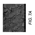
様々な堆積時間に対応する形態構造の評価は、走査型電子顕微鏡によって図7A〜図7Dに示すように試験した。図7Aは、多孔性ICCN複合材料を含む電極の一部のSEM画像を示す図である。図7Bは、図7AのSEM画像をより拡大した図である。図7Cは、電着したMnO2のナノフラワのSEM画像を示す図である。図7Dは、多孔性ICCN複合材料の断面のSEM画像を示す図である。 Evaluation of the morphological structure corresponding to various deposition times was tested by scanning electron microscopy as shown in FIGS. 7A-7D. FIG. 7A shows an SEM image of a portion of an electrode comprising a porous ICCN composite material. FIG. 7B is an enlarged view of the SEM image of FIG. 7A. FIG. 7C shows an SEM image of the electrodeposited MnO 2 nanoflower. FIG. 7D is a diagram showing an SEM image of a cross section of a porous ICCN composite material.
SEM顕微鏡写真は、120分の堆積によって準備した一般的なサンプルの概略的な形態構造と詳細な微細構造を示している。MnO2は、フィルム全体にわたり、グラフェン表面上に一様にコーティングした。さらに、電着したMnO2粒子により、MnO2とグラフェン基板との間にクリアな界面を有するナノフラワ形状のヒエラルキ構造が示されている。このことは、以前の研究では安定していた。MnO2ナノフラワの密な検査により、ナノフラワが、10〜20nmの厚さの極薄の数百のナノ破片で形成されていることが示された。これらナノ破片は、一体に相互接続されて、アクセス可能な表面積が大である中間の多孔性のMnO2を形成し、こうして、電解質に利用可能な複数の電気的に活性である場を提供し、これにより、迅速な表面の誘導電流反応を促す。 The SEM photomicrograph shows the schematic morphological structure and detailed microstructure of a typical sample prepared by 120 minute deposition. MnO 2 was uniformly coated on the graphene surface throughout the film. Furthermore, a nanoflower-like hierarchical structure having a clear interface between MnO 2 and the graphene substrate is shown by the electrodeposited MnO 2 particles. This has been stable in previous studies. A close examination of the MnO 2 nanoflowers showed that the nanoflowers were formed with hundreds of ultrathin nano-fragments with a thickness of 10-20 nm. These nano-fragments are interconnected together to form an intermediate porous MnO 2 with a large accessible surface area, thus providing multiple electrically active fields available for the electrolyte. This encourages a rapid surface induced current response.
ICCN/MnO2電極の3D構造を、図7Dの断面SEMを使用してさらに分析した。ICCNの3D多孔性構造は、凝集することなく、MnO2を堆積させた後に維持される。ICCN表面は、断面全体にわたってMnO2で一様にコーティングした。さらに、エネルギ分散性のX線分光学(EDS)により、C、O、及びMnの要素マップが提供される。これにより、3Dマクロ多孔性フレームワークを通してのMnO2の一様なコーティングが形成されたことを確認する。 The 3D structure of the ICCN / MnO 2 electrode was further analyzed using the cross-sectional SEM of FIG. 7D. The 3D porous structure of ICCN is maintained after depositing MnO 2 without agglomeration. The ICCN surface was uniformly coated with MnO 2 throughout the cross section. In addition, energy dispersive X-ray spectroscopy (EDS) provides C, O, and Mn element maps. This confirms that a uniform coating of MnO 2 was formed through the 3D macroporous framework.
XPSは首尾よく、ICCN/MnO2電極内のMnの化学組成及び酸化状態のよりよい理解のために使用された。Mn2p3/2のピークとMn2p1/2のピークは、11.6eVのスピンエネルギの分離を伴って、642.1eVと653.9eVとにそれぞれ位置しており、このことは、前に報告されたMn2p状態に関するデータに良好に一致している。Toupin et al.は、Mn3sダブレットのピークの分離は、酸化マンガンにおけるMnの酸化状態に関連しており、MnO、Mn3O4、Mn2O3、及びMnO2の参照サンプルが、それぞれ5.79eV、5.50eV、5.41eV、及び4.78eVの分離を示していることを示した。準備された状態のICCN/MnO2により、Mn3sのダブレットに関する4.8eVのエネルギ分離が示され、酸化物がMnO2であることを示唆している。このことは、O1sのスペクトルからさらに確認された。 XPS has been successfully used for a better understanding of the chemical composition and oxidation state of Mn in an ICCN / MnO 2 electrode. The Mn2p 3/2 and Mn2p 1/2 peaks are located at 642.1 eV and 653.9 eV, respectively, with a spin energy separation of 11.6 eV, which was reported previously. It is in good agreement with the data for the Mn2p state. Toupin et al. The separation of the Mn3s doublet peak is related to the oxidation state of Mn in manganese oxide, with reference samples of MnO, Mn 3 O 4 , Mn 2 O 3 , and MnO 2 being 5.79 eV, 5. It was shown to show separation of 50 eV, 5.41 eV, and 4.78 eV. The prepared ICCN / MnO 2 showed an energy separation of 4.8 eV for the Mn 3s doublet, suggesting that the oxide is MnO 2 . This was further confirmed from the O1s spectrum.
対称的なICCN/MnO2超コンデンサのアセンブリ及び電気化学的性能
ICCN/MnO2マクロ多孔性フレームワークの電気化学的性能をテストするために、超コンデンサのポーチセルを、Celgard M824のイオン多孔性セパレータによって分離し、1.0MのNa2SO4電解質で充填した、2つの対称的な電極から組み込んだ。セルは、1mV/s〜1000mV/sの広範囲のスキャンレートにわたって、サイクルボルタンメトリ(CV)によってテストした。例として、堆積時間3分のICCN/MnO2のサンプルを考慮すると、超コンデンサは、1000mV/sもの高さのスキャンレートの、ほぼ矩形のCVプロファイルを示し、優れた電荷貯蔵特性と、電極の超高速の反応を示している。様々な堆積時間で形成されたデバイスの静電容量は、CVプロファイルから計算した。静電容量は、単一の電極よりもむしろ、セルのスタックの総体積を使用して計算したことに留意されたい。これには、集電装置、作用物質、セパレータ、及び電解質の体積が含まれている。
Symmetric ICCN / MnO 2 Supercapacitor Assembly and Electrochemical Performance To test the electrochemical performance of the ICCN / MnO 2 macroporous framework, a supercapacitor pouch cell was constructed with Celgard M824 ionic porous separator. Incorporated from two symmetrical electrodes, separated and filled with 1.0 M Na 2 SO 4 electrolyte. The cell was tested by cycle voltammetry (CV) over a wide range of scan rates from 1 mV / s to 1000 mV / s. As an example, considering an ICCN / MnO 2 sample with a deposition time of 3 minutes, the supercapacitor exhibits a nearly rectangular CV profile with a scan rate as high as 1000 mV / s, with excellent charge storage properties, It shows a very fast reaction. The capacitance of devices formed at various deposition times was calculated from the CV profile. Note that the capacitance was calculated using the total volume of the stack of cells, rather than a single electrode. This includes current collectors, active substances, separators, and electrolyte volumes.
静電容量は、擬似容量性のMnO2の負荷量に大きく依存し、0〜960分の堆積時間とともに著しく増大する。たとえば、約203F/cm3ものスタックの静電容量は、960分の堆積時間におけるサンプルで達成され得る。このことは、電極毎の作用物質の体積のみに基づいて計算される場合、1136.5F/cm3の体積比容量となる。この値は、活性炭(60〜80F/cm3)、カーバイド誘導炭素(180F/cm3)、ベアICCN(12F/cm3)、活性MEGO(60F/cm3)、及び、液体を媒介とする化学的に変換されたグラフェン(liquid mediated chemically converted graphene)(CCG)フィルム(263.3F/cm3)の静電容量よりもかなり高く、カーボンベースの電極の体積比容量が、擬似容量性材料を組み込むことによって著しく増大し得ることを示している。さらに、この値は、MnO2ベースの超コンデンサに関して前に報告された最適値のいくつか、CNT/PPy/MnO2スポンジに関する16.1F/cm3、グラフェン/MnO2/CNTに関する130F/cm3、CNT/MnO2に関する246F/cm3、中間多孔性カーボン/MnO2に関する108F/cm3、及び過度に多孔性のカーボン/MnO2に関する90F/cm3よりも高い。さらに、堆積時間に応じて、デバイスのフットプリント毎の最大約0.8F/cm2もの過度に高い面積あたりの静電容量が達成され得る。このことは、好都合に、通常は約0.3F/cm2の静電容量を提供する、商業利用可能であるカーボン超コンデンサと比較する。 The capacitance is highly dependent on the loading of pseudocapacitive MnO 2 and increases significantly with a deposition time of 0-960 minutes. For example, a stack capacitance of about 203 F / cm 3 can be achieved with a sample at a deposition time of 960 minutes. This is a volumetric specific capacity of 1136.5 F / cm 3 when calculated based solely on the volume of the active substance per electrode. This value is based on activated carbon (60-80 F / cm 3 ), carbide derived carbon (180 F / cm 3 ), bare ICCN (12 F / cm 3 ), active MEGO (60 F / cm 3 ), and liquid-mediated chemistry. Significantly higher than the capacitance of chemically converted graphene (liquid converted chemically graphene) (CCG) film (263.3 F / cm 3 ), and the volume specific capacity of carbon-based electrodes incorporates pseudocapacitive materials It can be shown that this can be significantly increased. Moreover, this value, MnO 2 based several reported optimum above for ultracapacitors, CNT / PPy / MnO 2 16.1F / cm 3 relates sponge, graphene / MnO 2 / CNT about 130F / cm 3 , CNT / MnO 2 about 246F / cm 3, the intermediate porous carbon / MnO 2 about 108F / cm 3, and excessively higher than 90F / cm 3 relates porous carbon / MnO 2. Furthermore, depending on the deposition time, an excessively high capacitance per area as high as about 0.8 F / cm 2 per device footprint can be achieved. This is conveniently compared to a commercially available carbon supercapacitor that typically provides a capacitance of about 0.3 F / cm 2 .
この前例のない性能は、MnO2ナノフラワの寄与をICCN/MnO2電極の平均的な静電容量から分離することによって理解され得る。MnO2のみによって寄与される固有の静電容量は、Cs,MnO2=(QICCN/MnO2−QICCN)/(ΔV×mMnO2)の方程式に従って、ベアICCNの電荷を減じることによって計算した。ここで、Qはボルタメトリの電荷であり、ΔVは動作電位窓であり、mは質量である。MnO2の固有の静電容量は、作用物質の質量に応じ、1145F/gの最大値に達する。この最大値は、MnO2の13%の質量負荷における理論上の静電容量の約83%である。この驚くべき性能は、イオン及び電子の移送を促進し、電荷移行反応に十分な表面を提供する電極の微細構造に起因し得、作用物質のより高い利用を確実にする。 This unprecedented performance can be understood by separating the MnO 2 nanoflower contribution from the average capacitance of the ICCN / MnO 2 electrode. The intrinsic capacitance contributed solely by MnO 2 was calculated by subtracting the charge of bare ICCN according to the equation C s, MnO 2 = (Q ICCN / MnO 2 −Q ICCN ) / (ΔV × m MnO 2 ). Where Q is the voltammetric charge, ΔV is the operating potential window, and m is the mass. The intrinsic capacitance of MnO 2 reaches a maximum value of 1145 F / g depending on the mass of the active substance. The maximum value is about 83% of the capacitance of the theory in 13% of the mass loading of MnO 2. This surprising performance can be attributed to the microstructure of the electrode that facilitates ion and electron transport and provides a sufficient surface for the charge transfer reaction, ensuring higher utilization of the agent.
ICCN/MnO2マクロ多孔性電極の優れた特性を示すために、MnO2を、同じ条件下において、化学的に変換されたグラフェン(CCG)と、金の基板との両方にも電着した。CCG/MnO2がより低い静電容量を示すのみならず、その性能が、高い充電/放電の割合でかなり迅速に低下する。このことは、CCG電極の製造の際のグラフェンシートの再スタックに起因する場合があり、表面積が著しく低下することになり、最終的に、多孔の多くを塞ぐことになる。さらに、表面積及び構造的特性が制限されることから、Au/MnO2超コンデンサにより、極めて低い静電容量が示される。一方、ICCN/MnO2は、約50F/cm3のスタックの静電容量を示す。この静電容量は、CCG/MnO2の4倍より大であり、Au/MnO2より約3桁高い。ICCN/MnO2の向上した静電容量及びレートの能力により、有効なイオンの移動と、電気的に活性である高い表面積との両方の効果を相乗作用させる最適な構造をさらに確認し、こうして、高く可逆性である静電作用を、高い充電/放電量においてさえも可能にする。ICCNネットワークの最適化されたイオンの発散は、CCG電極に関する5952msに比べ、ICCNに関する23msの反応時間で、電気化学インピーダンス分光学から確認した。実際、ICCN/MnO2超コンデンサにより、商業利用可能である活性炭超コンデンサ、擬似コンデンサ、及びリチウム・イオン・ハイブリッド・コンデンサに比べ、優れた体積比容量とレートの能力が示されている。 In order to demonstrate the excellent properties of the ICCN / MnO 2 macroporous electrode, MnO 2 was electrodeposited on both chemically converted graphene (CCG) and a gold substrate under the same conditions. Not only does CCG / MnO 2 exhibit lower capacitance, but its performance declines fairly quickly at high charge / discharge rates. This may be due to the restacking of the graphene sheets during the production of the CCG electrode, resulting in a significant reduction in surface area and eventually plugging many of the porosity. Furthermore, due to the limited surface area and structural properties, the Au / MnO 2 supercapacitor exhibits very low capacitance. On the other hand, ICCN / MnO 2 exhibits a stack capacitance of about 50 F / cm 3 . This capacitance is greater than four times that of CCG / MnO 2 and about three orders of magnitude higher than Au / MnO 2 . The improved capacitance and rate capability of ICCN / MnO 2 further confirms the optimal structure that synergizes the effects of both effective ion migration and high surface area that is electrically active, thus Highly reversible electrostatic action is possible even at high charge / discharge rates. The optimized ion divergence of the ICCN network was confirmed from electrochemical impedance spectroscopy with a response time of 23 ms for ICCN compared to 5952 ms for the CCG electrode. In fact, ICCN / MnO 2 supercapacitors show superior volume specific capacity and rate capability compared to commercially available activated carbon supercapacitors, pseudocapacitors, and lithium ion hybrid capacitors.
非対称超コンデンサの形成
非対称超コンデンサの形成。非対称超コンデンサ(ASC)は、同じ電解質で良好に分離した電位窓で充電/放電され得る、異なるタイプの正極材料と負極材料とを利用する。これら材料は、正極において誘導電流反応を介して高容量が与えられ、負極におけるEDLメカニズムに起因して迅速な充電/放電が維持されることから、注目されている。さらに、非対称な構成により、水性の電解質の作動電圧窓を、水の熱力学的な限度(約1.2V)を超えて拡大することができ、水性の電解質を使用する対称的な超コンデンサよりも固有のエネルギが著しく高くなる。実際、水性の電解質を伴う、カーボン及びNiOOH電極をベースとする非対称の超コンデンサは、ここでは、ESMA−ELTONから商業利用可能である。しかし、この構成により、高い静電容量が確実になるが、セル電圧が低く(<1.5V)、このことは、この構成のエネルギ及び出力性能に不利である。ICCN/MnO2電極の高い擬似静電容量、及び、ICCN電極の2層の静電容量の迅速な充電/放電を考慮して、非対称超コンデンサを、ICCN/MnO2を正極、ICCNを負極として使用して組み立てた。ここで、2つの電極間の充電バランスは、正極におけるMnO2の堆積時間と、負極におけるグラフェンフィルムの厚みとを制御することによって達成した。正極セルに関して、13%のMnO2の質量の負荷(3分の堆積時間)を伴うICCN/MnO2を使用する、非対称なセルの電気化学的性能により、ほぼ矩形のCVプロファイルで、高度に三角形形状のCCカーブの、理想的な静電容量の作用が示される。CVプロファイルは、10,000mV/sの過度に高いレートにもなる、スキャンレートの増大を伴い、明らかな歪曲のない矩形形状を保持し、この非対称超コンデンサの高いレート能力を示している。興味深いことに、非対称セルにより、高いエネルギ密度を有するものとされる、水性の電解質における2.0Vにもなる広く安定した作動電位窓が提供される。さらに、MnO2の堆積時間が3分から960分に増大するにつれて、スタックの静電容量は、約3F/cm3から76F/cm3に著しく増大する。このことは、貯蔵されたエネルギ及び電力が非対称の構造において大きく向上し得ることを意味している。これらセルは、より迅速な充電速度及び放電速度が必要とされる場合も、その高容量を保持することができる。形成された超コンデンサは柔軟性が高く、デバイスの構造的な完全性に影響することなく、折曲げ、ねじることができる。さらに、超コンデンサにより、高度に折り曲げられた条件下に置かれた場合であっても、ほぼ同じ容量を示し、可撓性の電子機器のための実際的なエネルギ貯蔵システムとして期待できる。
Formation of asymmetric supercapacitor Formation of asymmetric supercapacitor. Asymmetric supercapacitors (ASCs) utilize different types of positive and negative electrode materials that can be charged / discharged with a well-separated potential window with the same electrolyte. These materials are attracting attention because they are given high capacity via an induced current reaction at the positive electrode and maintain rapid charge / discharge due to the EDL mechanism at the negative electrode. In addition, the asymmetric configuration allows the operating voltage window of the aqueous electrolyte to be expanded beyond the thermodynamic limit of water (approximately 1.2V), more than a symmetric supercapacitor using an aqueous electrolyte. However, the intrinsic energy is significantly increased. In fact, asymmetric supercapacitors based on carbon and NiOOH electrodes with an aqueous electrolyte are commercially available here from ESMA-ELTON. However, this configuration ensures high capacitance, but the cell voltage is low (<1.5V), which is detrimental to the energy and output performance of this configuration. Considering the high pseudo-capacitance of the ICCN / MnO 2 electrode and the quick charge / discharge of the two-layer capacitance of the ICCN electrode, the asymmetric supercapacitor is made with ICCN / MnO 2 as the positive electrode and ICCN as the negative electrode. Assembled using. Here, the charge balance between the two electrodes was achieved by controlling the deposition time of MnO 2 on the positive electrode and the thickness of the graphene film on the negative electrode. For the positive cell, the electrochemical performance of the asymmetric cell using ICCN / MnO 2 with a mass load of 13% MnO 2 (3 min deposition time), highly triangular with a nearly rectangular CV profile The ideal capacitance effect of the shape CC curve is shown. The CV profile shows the high rate capability of this asymmetric supercapacitor, keeping the rectangular shape without obvious distortion, with increasing scan rate, which can be an excessively high rate of 10,000 mV / s. Interestingly, the asymmetric cell provides a wide and stable working potential window as high as 2.0 V in an aqueous electrolyte that is supposed to have a high energy density. Furthermore, as the deposition time of MnO 2 increases from 3 minutes to 960 minutes, the stack capacitance increases significantly from about 3 F / cm 3 to 76 F / cm 3 . This means that the stored energy and power can be greatly improved in asymmetric structures. These cells can retain their high capacity when more rapid charge and discharge rates are required. The formed supercapacitor is highly flexible and can be folded and twisted without affecting the structural integrity of the device. Further, the supercapacitor can be expected to be a practical energy storage system for flexible electronic devices that exhibits almost the same capacity even when placed under highly bent conditions.
長いサイクル寿命は、商業上実用的な超コンデンサに関する別の重要な特徴である。むしろ、非対称超コンデンサは、1000mV/sの高いスキャンレートで10,000回の充電/放電サイクルのテストをした後に、その元々の容量の96%を超える容量を維持することから、非常に安定している。超コンデンサの等価直列抵抗(ESR)を、サイクルの間、ナイキスト線図を使用して監視した。本デバイスは、最初の1000サイクルでわずかなESRの増大を示し、残りのサイクルにわたって微細に変化したのみである。 Long cycle life is another important feature for commercially practical supercapacitors. Rather, the asymmetric supercapacitor is very stable because it maintains over 96% of its original capacity after testing 10,000 charge / discharge cycles at a high scan rate of 1000 mV / s. ing. Supercapacitor equivalent series resistance (ESR) was monitored during the cycle using a Nyquist diagram. The device showed a slight increase in ESR in the first 1000 cycles and only changed slightly over the remaining cycles.
3次元のかみ合ったマイクロ超コンデンサ
3次元のかみ合ったマイクロ超コンデンサ。スマートセンサ、インプラント可能な医療デバイス、及び微小電気機械システム(MEMS)などの小型化した電子システムの開発は、限られたスペースでの高いエネルギ密度の、微小スケールの超コンデンサに関する需要の増大に繋がってきた。この特性は、現代の電子用途のためのエネルギ貯蔵デバイスの小型化において極めて重要である。事前の調査では、活性炭、グラフェン、カーボンナノチューブ、ポリマ、及び金属酸化物などの様々な作用物質を使用することにより、マイクロ超コンデンサのエネルギ密度の増大に注目してきた。フットプリントエリア毎の容量が高いマイクロ超コンデンサの開発は、現代の電子用途のためのエネルギ貯蔵デバイスの小型化において極めて重要である。残念ながら、現在の最新技術のシステムは、依然として、カーボンに関する11.6mF/cm2未満、導電性ポリマに関する78mF/cm2未満、金属酸化物に関する56.3mF/cm2未満の、面積あたりの容量が低いことに難点がある。新しいハイブリッドマイクロ超コンデンサを形成した。このコンデンサでは、正極と負極とが3Dのかみ合った構造に分割されている。この構造は、「トップダウン」の光スクライビングリソグラフィの技術と「ボトムアップ」の選択的電着を組み合わせることによって達成した。最初に、3Dのかみ合ったICCN微小電極を、消費者のグレードの光スクライビングのDVDバーナを使用した、グラフェンパターンのGOフィルム上への直接の書込によって製造した。形成されたデバイスは、ほぼ絶縁されたGOによって分割された平面内の16の微小電極(8つの正極と8つの負極)を備えており、微小電極間の距離は、イオン伝達路を短く維持するのに十分に近くなっている。したがって、MnO2ナノフラワを、基本的な3セルのセットアップを使用して、ICCN微小電極の1つのセット上に選択的に電着した。微小電極の幅は、微小デバイスの正極と負極との間の電荷にマッチするように調整される。より明るい微小電極は、ベアグラフェン(負極)に対応し、一方、他方側は、MnO2の電着の後に色が暗くなる(正極)。光学的な顕微鏡画像により、良好に規定されたパターン、及び、微小電極間のシャープな境界が示される。
Three-dimensional meshed micro supercapacitor Three-dimensional meshed micro supercapacitor. The development of miniaturized electronic systems such as smart sensors, implantable medical devices, and microelectromechanical systems (MEMS) has led to increased demand for high energy density, small scale supercapacitors in confined spaces. I came. This property is extremely important in the miniaturization of energy storage devices for modern electronic applications. Prior research has focused on increasing the energy density of micro supercapacitors by using various agents such as activated carbon, graphene, carbon nanotubes, polymers, and metal oxides. The development of high-capacity micro supercapacitors per footprint area is extremely important in the miniaturization of energy storage devices for modern electronic applications. Unfortunately, current state-of-the-art systems still have capacities per area of less than 11.6 mF / cm 2 for carbon, less than 78 mF / cm 2 for conductive polymers, and less than 56.3 mF / cm 2 for metal oxides. There is a difficulty in being low. A new hybrid micro supercapacitor was formed. In this capacitor, the positive electrode and the negative electrode are divided into a 3D meshing structure. This structure was achieved by combining “top-down” optical scribing lithography techniques with “bottom-up” selective electrodeposition. Initially, 3D mated ICCN microelectrodes were fabricated by direct writing of graphene patterns onto GO films using a consumer grade light scribing DVD burner. The formed device has 16 microelectrodes (8 positive and 8 negative) in a plane divided by a substantially insulated GO, and the distance between the microelectrodes keeps the ion transfer path short. It ’s close enough. Therefore, MnO 2 nanoflowers were selectively electrodeposited on one set of ICCN microelectrodes using a basic three-cell setup. The width of the microelectrode is adjusted to match the charge between the positive and negative electrodes of the microdevice. The brighter microelectrode corresponds to bare graphene (negative electrode), while the other side becomes darker after positive electrodeposition of MnO 2 (positive electrode). Optical microscopic images show well defined patterns and sharp boundaries between microelectrodes.
電気化学的特性により、非対称な微小超コンデンサが、慣習的な挟み込むタイプの非対称超コンデンサに比べ、体積比容量及びレート能力を向上させたことが示された。対称なハイブリッドマイクロ超コンデンサは、400mF/cm2に近付く面積あたりの静電容量と同様の作用を示す。このことは、電極間の短絡を避けるために、挟み込まれた構造に通常使用されるポリマセパレータの必要性を除去することにより、容量のパッキング効率がよりよくなる、微小デバイスの平坦な構造に起因すると考えられる。さらに、デバイスの微小スケールの構造は、2つの微小電極間の中間のイオンの発散経路が著しく低減されることになる。このことは、すべてのグラフェンのマイクロ超コンデンサの前の結果と一致している。このことは、かみ合ったマイクロ超コンデンサにおいて現在達成されているもっとも高い面積あたりの静電容量であると考えられている。スタックの静電容量は約250F/cm3(電極毎の体積比容量は1197F/cm3)に著しく向上する。このことは、EDLC、擬似超コンデンサ、及びハイブリッドマイクロ超コンデンサに関して前に報告されていた値、カーボンオニオンに関する1.3F/cm3、グラフェンに関する2.35〜3.05F/cm3、CNTに関する1.08F/cm3、グラフェン/CNTに関する3.1F/cm3、カーバイド誘導炭素に関する180F/cm3(電極)、ポリアニリンナノファイバに関する588F/cm3、バナジウムの二硫化物のナノシートに関する317F/cm3(電極)、モリブデンの二硫化物のナノシートに関する178F/cm3よりもかなり高い。 Electrochemical properties have shown that asymmetric micro supercapacitors have improved volumetric capacity and rate capability compared to conventional sandwich type asymmetric supercapacitors. Symmetric hybrid micro supercapacitors exhibit a similar effect with capacitance per area approaching 400 mF / cm 2 . This is due to the flat structure of the microdevice, which eliminates the need for polymer separators commonly used in the sandwiched structure to avoid shorting between the electrodes, resulting in better capacity packing efficiency. Conceivable. Furthermore, the microscale structure of the device will significantly reduce the intermediate ion divergence path between the two microelectrodes. This is consistent with previous results for all graphene micro-supercapacitors. This is believed to be the highest capacitance per area currently achieved in meshed micro supercapacitors. The capacitance of the stack is significantly improved to about 250 F / cm 3 (volume specific capacity per electrode is 1197 F / cm 3 ). This is, EDLC, pseudo supercapacitors, and values have been reported previously for a hybrid micro supercapacitors, 1.3F / cm 3 regarding carbon onion, about 2.35~3.05F / cm 3, CNT relates graphene 1 .08F / cm 3, 3.1F / cm 3 relates graphene / CNT, 180F / cm 3 relates carbide-derived carbon (electrode), 588F / cm 3 relates polyaniline nanofibers, 317F / cm 3 regarding nanosheet disulfide vanadium (Electrode), much higher than 178 F / cm 3 for molybdenum disulfide nanosheets.
議論
ICCN/MnO2ベースの超コンデンサのエネルギ及び出力密度は、現在の技術より優れている。これらの結果を現状の技術の見方に取り入れるために、商業利用可能である複数のカーボンベースの超コンデンサ、擬似コンデンサ、ハイブリッド超コンデンサ、及びLiイオン・ハイブリッド・コンデンサを特徴付けた。これらデバイスは、ICCN/MnO2と同じ動的条件下でテストした。すべてのデバイスに関して、集電装置、作用物質、セパレータ、及び電解質を含むセル全体の体積に基づいて計算した。ハイブリッドICCN/MnO2のエネルギ密度は、構成(対称、非対称、及び、挟みこまれているか、かみ合っている)ならびにMnO2の質量負荷に応じて、22Wh/lから42Wh/lの間で変化する。比較により、ICCN/MnO2ハイブリッド超コンデンサは、現行の技術の商業利用可能であるEDLCカーボン超コンデンサの容量の約6倍を貯蔵する。これら超コンデンサはやはり、擬似コンデンサ、ハイブリッド超コンデンサ、及び超コンデンサ/リチウム・イオン・バッテリ・ハイブリッド(Liイオンコンデンサ)よりも優れている。さらに、ICCN/MnO2超コンデンサは、約10kW/lもの出力密度を提供することができる。このことは、高出力鉛蓄電池の100倍速く、リチウム薄膜電池の1000倍速い。
Discussion The energy and power density of ICCN / MnO 2 based supercapacitors are superior to current technology. In order to incorporate these results into the current state of the art, several carbon-based supercapacitors, pseudocapacitors, hybrid supercapacitors, and Li-ion hybrid capacitors that are commercially available were characterized. These devices were tested under the same dynamic conditions as ICCN / MnO 2 . For all devices, calculations were based on the total cell volume, including current collector, agent, separator, and electrolyte. The energy density of the hybrid ICCN / MnO 2 varies between 22 Wh / l and 42 Wh / l, depending on the configuration (symmetric, asymmetric, and pinched or meshed) and the mass load of MnO 2 . By comparison, the ICCN / MnO 2 hybrid supercapacitor stores approximately 6 times the capacity of the current technology commercially available EDLC carbon supercapacitor. These supercapacitors are still superior to pseudocapacitors, hybrid supercapacitors, and supercapacitors / lithium ion battery hybrids (Li ion capacitors). Furthermore, ICCN / MnO 2 supercapacitors can provide power densities as high as about 10 kW / l. This is 100 times faster than high power lead acid batteries and 1000 times faster than lithium thin film batteries.
高電圧の要請を満たすために、超コンデンサはしばしば、ともに直列に接続されたセル層に入れられる。これにより、いくつかの場合では適切である、大型の超コンデンサモジュールになるが、出力源の全体のサイズが重要である用途では、しばしば問題を生じる。本明細書に提案されているのは、別々の電気化学的セルのアレイが、同じ平面に1ステップで直接形成されている、異なる設計である。この構成により、電圧及び電流の出力にわたる非常に良好な制御が示される。さらに、このアレイは、有効な太陽エネルギの収集及び貯蔵のための太陽電池に組み込むことができる。 To meet the high voltage requirements, supercapacitors are often placed in cell layers connected together in series. This results in a large supercapacitor module that is appropriate in some cases, but is often problematic in applications where the overall size of the output source is important. Proposed here are different designs in which an array of separate electrochemical cells is formed directly in the same plane in one step. This configuration shows very good control over voltage and current output. Furthermore, the array can be incorporated into solar cells for effective solar energy collection and storage.
まとめると、本開示により、コンパクトで、信頼性があり、エネルギ密度が高く、迅速に充電され、寿命が長い、ハイブリッドICCN/MnO23次元超コンデンサ及びマイクロ超コンデンサの製造のための、シンプルで拡縮可能なアプローチが提供される。MnO2がアルカリ電池に広く使用されている(毎年約100億ユニットを販売している(34))ことと、カーボンベースの材料の拡張性が考えられる。具体的には、ICCN/MnO2ハイブリッド電極に、実際の世界の用途が見込まれる。 In summary, the present disclosure provides a simple, reliable, reliable, high energy density, fast charge, long life, hybrid ICCN / MnO 2 3D super capacitor and micro super capacitor manufacturing. A scalable approach is provided. MnO 2 is widely used in alkaline batteries (sold about 10 billion units each year (34)) and the expandability of carbon-based materials is considered. Specifically, real world applications are expected for ICCN / MnO 2 hybrid electrodes.
材料及び方法
ICCN/MnO2、Au/MnO2、及びCCG/MnO2電極の合成
ICCNは、光スクライビングDVDバーナからのレーザビームを酸化黒鉛でコーティングされたDVDディスク上に収束させることによって準備した。第1に、DVDディスクを、金でコーティングされたポリイミドのフィルム(Astral Technology Unlimited,Inc.)か、ポリエチレンテレフタレートのシートでカバーした。このディスクは、ドクターブレード技術を使用して水中に分散した2%のGOでコートし、周囲の条件下で5時間、乾燥させた。コンピュータでデザインした画像を酸化黒鉛上にプリントして、適切なICCNパターンを形成する。この後に、標準的な3電極のセットアップを使用して、0.1MのNaNO3の水溶液内の0.02MのMn(NO3)2からのMnO2の電着を行った。ここで、ICCNのピース(1cm2)を作動電極として、Ag/AgClを基準電極(BASi,Indiana,USA)として、白金フォイル(2cm2、Sigma−Aldrich)を対電極として使用した。堆積は、250μA/cm2の一定の電流を、3分から960分の様々な時間だけ印加することによって達成した。電着の後に、作動電極をDI水で十分に洗浄し、余分な電解質を除去し、オーブン内で、60℃で1時間乾燥させた。ICCN上に堆積したMnO2の量は、1μgの可読性の、高精度の微量天秤(Mettler Toledo,MX5)を使用して、電着の前後の電極の重量差から判定した。
Materials and Methods Synthesis of ICCN / MnO 2 , Au / MnO 2 , and CCG / MnO 2 Electrodes ICCN was prepared by converging a laser beam from an optical scribing DVD burner onto a DVD disc coated with graphite oxide. First, a DVD disc was covered with a gold coated polyimide film (Astral Technology Unlimited, Inc.) or a sheet of polyethylene terephthalate. The disc was coated with 2% GO dispersed in water using a doctor blade technique and dried for 5 hours under ambient conditions. A computer designed image is printed on graphite oxide to form an appropriate ICCN pattern. This was followed by electrodeposition of MnO 2 from 0.02M Mn (NO 3 ) 2 in an aqueous solution of 0.1M NaNO 3 using a standard three-electrode setup. Here, ICCN pieces (1 cm 2 ) were used as working electrodes, Ag / AgCl was used as a reference electrode (BASi, Indiana, USA), and platinum foil (2 cm 2 , Sigma-Aldrich) was used as a counter electrode. Deposition was achieved by applying a constant current of 250 μA / cm 2 for various times from 3 minutes to 960 minutes. After electrodeposition, the working electrode was thoroughly washed with DI water to remove excess electrolyte and dried in an oven at 60 ° C. for 1 hour. The amount of MnO 2 deposited on the ICCN was determined from the difference in weight of the electrodes before and after electrodeposition using a 1 μg readable, high precision microbalance (Mettler Toledo, MX5).
比較のために、MnO2は、金でコーティングしたポリイミド及びグラフェン(CCG)紙などの他の基板上に電着した。金でコーティングされたポリイミドは、Astral Technology Unlimited,Inc.(Minnesota,USA)から取得し、さらなる処理を施すことなく使用した。グラフェン紙は、我々が前に報告した方法に従って製造した。金でコーティングされたポリイミド及びグラフェン紙は、上述の条件と同じ条件下でのMnO2のさらなる電着のために、1cm2の矩形ストリップにカットした。 For comparison, MnO 2 was electrodeposited on other substrates such as gold coated polyimide and graphene (CCG) paper. Gold coated polyimides are available from Astral Technology Unlimited, Inc. (Minnesota, USA) and used without further processing. Graphene paper was manufactured according to the method we reported previously. Gold coated polyimide and graphene paper were cut into 1 cm 2 rectangular strips for further electrodeposition of MnO 2 under the same conditions as described above.
挟み込むタイプのハイブリッド超コンデンサの組立て
慣習的な挟み込む構造のハイブリッド超コンデンサは、前セクションで準備した電極を使用して組み立てた。対称的な超コンデンサと非対称の超コンデンサとの両方を形成した。対称的な超コンデンサは、1.0MのNa2SO4水溶液を電解質として使用して、2つの同一の電極間に、Celgard M824(Celgard,North Carolina,USA)セパレータを挟み込むことによって組み立てた。非対称構造では、ICCN/MnO2を正極として使用し、ICCNを負極として使用した。ICCNベースの超コンデンサ及びCCGベースの超コンデンサに関し、ステンレス鋼(または銅)テープを、銀色ペイントを使用して、集電装置として電極に取り付けた。組立ての前に、適切な湿潤を確実にするために、電極を電解質内に1時間浸した。
Assembling the sandwich type hybrid supercapacitor The conventional sandwich structure hybrid supercapacitor was assembled using the electrodes prepared in the previous section. Both symmetric and asymmetric supercapacitors were formed. Symmetrical supercapacitors, using Na 2 SO 4 aqueous solution of 1.0M as an electrolyte, between two identical electrodes, Celgard M824 (Celgard, North Carolina , USA) was assembled by sandwiching the separator. In the asymmetric structure, ICCN / MnO 2 was used as the positive electrode and ICCN was used as the negative electrode. For ICCN-based supercapacitors and CCG-based supercapacitors, stainless steel (or copper) tape was attached to the electrodes as a current collector using silver paint. Prior to assembly, the electrode was immersed in the electrolyte for 1 hour to ensure proper wetting.
かみ合ったハイブリッドマイクロ超コンデンサの形成
マイクロ超コンデンサの形成プロセスは、図5Bに示されており、また、以下に記載する。第1に、ICCNのかみ合った微小電極は、消費者のグレードのDVDバーナを使用して、金でコーティングされたポリイミド(またはポリエチレンテレフタレート)基板上に支持されたGOフィルム上に直接プリントした。第2に、上述の電着セットアップを使用して、MnO2ナノフラワを、1つのセットのかみ合った電極の上に生成した。印加電流を、250μA/cm2の電流密度で作動ICCNの堆積エリアに対して標準化し、質量負荷を、堆積時間を調整することによって制御した。同様に、正極と負極との両方としてのICCN/MnO2ベースの対称的なマイクロ超コンデンサも準備した。ここで、製造プロセスは、かみ合ったベアICCN電極の(1つのサイドの代わりに)2つのサイドが、銅テープを使用してともに接続され、電着の間、作動電極として使用したことを除き、同一である。
Interdigitated Hybrid Micro Supercapacitor Formation The process of forming a micro supercapacitor is shown in FIG. 5B and is described below. First, ICCN interdigitated microelectrodes were printed directly onto a GO film supported on a gold-coated polyimide (or polyethylene terephthalate) substrate using a consumer grade DVD burner. Second, using the electrodeposition setup described above, MnO 2 nanoflowers were generated on a set of mated electrodes. The applied current was normalized to the deposition area of the working ICCN at a current density of 250 μA / cm 2 and the mass load was controlled by adjusting the deposition time. Similarly, a symmetrical micro supercapacitor based on ICCN / MnO 2 as both positive and negative electrodes was also prepared. Here, the manufacturing process, except that the two sides of the mating bare ICCN electrode (instead of one side) were connected together using copper tape and used as the working electrode during electrodeposition, Are the same.
本開示に実施されるハイブリッド電極により、後の参照リストに示された、特許されたか開示された方法のいずれのものよりも高いエネルギ及び電力を提供することができる。本開示の電極は、やはり、同じ条件下でテストされた、商業利用可能である、カーボンベースの超コンデンサ、擬似コンデンサ、ハイブリッド超コンデンサ、及びリチウム・イオン・コンデンサよりも優れている。 The hybrid electrode implemented in the present disclosure can provide higher energy and power than any of the patented or disclosed methods shown in the later reference list. The electrodes of the present disclosure are also superior to commercially available carbon-based supercapacitors, pseudocapacitors, hybrid supercapacitors, and lithium ion capacitors that have been tested under the same conditions.
本開示は、これらハイブリッド超コンデンサを微小スケールに小型化するための容易な技術を記載している。これらマイクロ超コンデンサにより、400mF/cm2を超える、過度に高い面積あたりの静電容量が可能になる。この静電容量は、前の開示及び特許出願における、現在達成されているいずれの性能よりも高い。ハイブリッド超コンデンサは、リチウム薄フィルム電池の2倍よりも大きい22Wh/lのエネルギ密度をも提供することができる。明らかに、ハイブリッド超コンデンサは、関連技術に比べて有利である。 This disclosure describes an easy technique for miniaturizing these hybrid supercapacitors to a microscale. These micro supercapacitors allow an excessively high capacitance per area exceeding 400 mF / cm 2 . This capacitance is higher than any currently achieved performance in previous disclosures and patent applications. The hybrid supercapacitor can also provide an energy density of 22 Wh / l, which is greater than twice that of a lithium thin film battery. Clearly, hybrid supercapacitors are advantageous over the related art.
別の問題は、通常は3Vより低い、既存の超コンデンサの作動電圧である。一方、通常の電子装置の用途に使用されるコンデンサは、通常、数ボルトから1kVの範囲である。この問題を解決するために、本開示は、限定ではないが、電気化学的セルのアレイが、同じ平面に1ステップで直接形成されている、異なる設計である一実施形態を記載している。この構成により、6Vの作動電圧窓が提供される。さらに、本開示には、電圧をさらに増大させるための方針が記載されている。これらアレイは、有効な太陽エネルギの収集及び貯蔵システムを製造するために、太陽電池に組み込むことができる。 Another problem is the operating voltage of existing supercapacitors, usually below 3V. On the other hand, capacitors used for normal electronic device applications are typically in the range of a few volts to 1 kV. To solve this problem, the present disclosure describes, but is not limited to, an embodiment that is a different design in which an array of electrochemical cells is formed directly in the same plane in one step. This configuration provides an operating voltage window of 6V. In addition, this disclosure describes a strategy for further increasing the voltage. These arrays can be incorporated into solar cells to produce an effective solar energy collection and storage system.
本開示に記載のハイブリッド超コンデンサの使用には、限定ではないが、以下の範囲が含まれる。
1.たとえば携帯電話、コンピュータ、カメラである、ポータブル電子装置。
2.ペースメーカ、除細動器、補聴器、苦痛除去デバイス、及び薬ポンプを含む、生命維持及び生命向上のための医療デバイスである、医療デバイス。
3.電気自動車。耐用年数が長い高出力の電池が、電気自動車の産業の向上のために必要とされている。
4.宇宙。耐用年数の長い高出力の電池を、探査機、着陸船、宇宙服、及び電子設備を含む宇宙システムに給電するために、宇宙で使用することができる。
5.軍事用電池。軍は、大量の電子装置及び設備に給電するために、特別な電池を使用している。もちろん、質量/体積の低減がかなり好ましい。
6.電気が太陽電池またはバッテリから来る、内燃機関よりもむしろ電気モータで作動する航空機である、電気航空機。
7.グリッドスケールのエネルギ貯蔵装置。電池は、(発電所からの)生産が消費を超える際に電気エネルギを貯蔵するのに使用され、貯蔵されたエネルギは、消費が生産を超える際に、場合によって使用される。
8.再生可能エネルギ。夜間には太陽によって照らされず、風は常に吹いているわけではないことから、電池は、日没後の時間の間、及び、風が吹いていない場合に使用するために、再生可能エネルギ源からの過剰の電力を貯蔵するための、電力系統ではない電力システムに用途を見出した。もちろん、高出力の電池は、現行の最新技術の電池よりも高効率で太陽電池からエネルギを収集する。
9.電動工具。耐用年数の長い高出力電池により、ドリル、スクリュードライバ、ノコギリ、レンチ、及びグラインダなどの、コードレス電動工具の迅速な充電が可能になる。現行の電池の問題は、再充電時間が長いことである。
10.小型化した電子装置。微小スケールのハイブリッド超コンデンサは、フットプリント毎の高容量が重要である、微小電気機械システム(MEMS)、スマートセンサ、インプラント可能な医療デバイス、及び無線認識(RFID)タグなどのマイクロ電子デバイスに電力を提供するのに使用することができる。
Use of the hybrid supercapacitors described in this disclosure includes, but is not limited to, the following ranges.
1. Portable electronic devices such as mobile phones, computers and cameras.
2. A medical device that is a medical device for life support and life enhancement, including a pacemaker, a defibrillator, a hearing aid, a pain relief device, and a drug pump.
3. Electric car. High power batteries with a long service life are needed to improve the electric vehicle industry.
4). space. Long-life, high-power batteries can be used in space to power space systems including spacecraft, landers, space suits, and electronic equipment.
5. Military battery. The military uses special batteries to power a large number of electronic devices and equipment. Of course, a mass / volume reduction is quite preferred.
6). An electric aircraft, which is an aircraft that operates with an electric motor rather than an internal combustion engine, where the electricity comes from solar cells or batteries.
7). Grid scale energy storage device. Batteries are used to store electrical energy when production (from a power plant) exceeds consumption, and the stored energy is optionally used when consumption exceeds production.
8). Renewable energy. Because it is not illuminated by the sun at night and the wind is not always blowing, the battery is removed from renewable energy sources for use during the hours after sunset and when the wind is not blowing. The present invention has found an application in a power system that is not a power system for storing excess power. Of course, high power batteries collect energy from solar cells more efficiently than current state-of-the-art batteries.
9. Electric tool. Long-life, high-power batteries allow for quick charging of cordless power tools such as drills, screwdrivers, saws, wrenches, and grinders. The problem with current batteries is the long recharge time.
10. A miniaturized electronic device. Microscale hybrid supercapacitors power microelectronic devices such as microelectromechanical systems (MEMS), smart sensors, implantable medical devices, and radio frequency identification (RFID) tags, where high capacitance per footprint is important. Can be used to provide.
超コンデンサは、ここでは、ハイブリッド自動車及び電気自動車、大衆消費電子製品、ならびに、軍事及び宇宙の用途での進展において、重要な役割を果たしている。現行の世代のカーボンベースの超コンデンサにおけるエネルギ密度の制限を克服するために、ハイブリッド超コンデンサシステムを開発することの要請が高まっている。ここで、我々は、合理的に電極の微細構造を設計し、作用物質を、高電圧で作動する電解質と組み合わせることにより、グラフェン及びMnO2をベースとする、3Dの高性能のハイブリッド超コンデンサ及びマイクロ超コンデンサを示す。このことは、1100F/cm3を超える過度に高い体積比容量のハイブリッド電極の結果となった。このことは、1380F/gの理論値に近い、1145F/gを形成するMnO2の固有の静電容量に対応する。デバイス全体のエネルギ密度は、デバイスの構成に応じて、22Wh/lから42Wh/lの間で変化する。このエネルギ密度は、同じ条件下でテストした、商業利用可能である2層の超コンデンサ、擬似コンデンサ、リチウム・イオン・コンデンサ、及びハイブリッド超コンデンサのエネルギ密度より優れており、鉛蓄電池のエネルギ密度に匹敵する。これらハイブリッド超コンデンサは、水性の電解質を使用し、今日の超コンデンサを構築するのに必要である、高価な「乾燥室」を必要とすることなく、空気中で組み立てられる。さらに、我々は、高電圧の用途のための超コンデンサアレイの製造のためのシンプルな技術を示す。これらアレイは、有効なエネルギの収集及び貯蔵システムのために、太陽電池に組み込むことができる。 Supercapacitors play an important role here in developments in hybrid and electric vehicles, consumer electronics, and military and space applications. In order to overcome the energy density limitations in the current generation of carbon-based supercapacitors, there is an increasing demand to develop hybrid supercapacitor systems. Here, we rationally design the microstructure of the electrode and combine the active substance with an electrolyte operating at high voltage, to make a 3D high performance hybrid supercapacitor based on graphene and MnO 2 and A micro super capacitor is shown. This resulted in a hybrid electrode with an excessively high volumetric capacity exceeding 1100 F / cm 3 . This corresponds to the inherent capacitance of MnO 2 forming 1145 F / g, which is close to the theoretical value of 1380 F / g. The energy density of the entire device varies between 22 Wh / l and 42 Wh / l depending on the device configuration. This energy density is superior to the energy density of commercially available two-layer supercapacitors, pseudocapacitors, lithium-ion capacitors, and hybrid supercapacitors tested under the same conditions. Comparable. These hybrid supercapacitors are assembled in air using an aqueous electrolyte and without the need for the expensive “drying chamber” required to build today's supercapacitors. In addition, we present a simple technique for the manufacture of supercapacitor arrays for high voltage applications. These arrays can be incorporated into solar cells for effective energy collection and storage systems.
現代の生活の急速に増大するエネルギの需要の結果として、高性能のエネルギ貯蔵デバイスの開発がかなり注目されてきている。超コンデンサは、これら電池と、慣習的なコンデンサとの間の中間の特性のエネルギ貯蔵デバイスが見込めるが、これらは今までより急速に向上している。過去数十年にわたり、超コンデンサは、ますます多くの用途において電池及びコンデンサと置き換わることにより、日々の製品の重要な構成要素となってきている。これらの高い出力密度及び優れた低温性能により、これら超コンデンサを、バックアップ動力、コールドスタート、フラッシュカメラ、回生制動、及びハイブリッド電気自動車のための技術の選択肢となってきている。この技術の将来における成長は、エネルギ密度、出力密度、カレンダ、及びサイクルライフ、ならびに製造コストに依存する。 As a result of the rapidly increasing demand for energy in modern life, the development of high performance energy storage devices has received considerable attention. Supercapacitors are expected to have energy storage devices with intermediate characteristics between these batteries and conventional capacitors, but these are improving more rapidly than ever. Over the past decades, supercapacitors have become an important component of everyday products by replacing batteries and capacitors in an increasing number of applications. These high power densities and excellent low temperature performance make these supercapacitors a technology choice for backup power, cold start, flash camera, regenerative braking, and hybrid electric vehicles. The future growth of this technology depends on energy density, power density, calendar and cycle life, and manufacturing costs.
これらの電荷貯蔵メカニズムによれば、超コンデンサは、電気2層コンデンサ(EDLC)または擬似コンデンサのいずれかに分類される。EDLCでは、電荷は、高表面積カーボン材料上の電解質イオンの急速な吸収/吐出を通して貯蔵される。一方、擬似コンデンサは、金属酸化物または導電性ポリマの表面の近位の、急速かつ可逆的な誘導電流反応を介して電荷を貯蔵する。市場において現在利用可能である超コンデンサの大多数は、2.7V(2)もの高さのセル電圧を提供する、活性炭電極及び有機電解質を特徴とする対称なEDLCである。商業利用可能であるEDLCが高出力密度及び優れたサイクル寿命を示すが、これらEDLCは、カーボンベースの電極の静電容量が制限されているために、エネルギ密度が低いことが欠点である。特定の誘導電流電極の擬似静電容量(通常は300〜1000F/g)は、カーボンベースのEDLCの静電容量を超えるが、それらの性能は、繰返しによってすぐに低下する傾向にある(2−4)。 According to these charge storage mechanisms, supercapacitors are classified as either electric double layer capacitors (EDLC) or pseudocapacitors. In EDLC, charge is stored through rapid absorption / discharge of electrolyte ions on high surface area carbon materials. On the other hand, pseudocapacitors store charge via a rapid and reversible induced current reaction proximal to the surface of the metal oxide or conductive polymer. The majority of supercapacitors currently available in the market are symmetric EDLCs featuring activated carbon electrodes and organic electrolytes that provide cell voltages as high as 2.7V (2). Although commercially available EDLCs exhibit high power density and excellent cycle life, these EDLCs have the disadvantage of low energy density due to the limited capacitance of carbon-based electrodes. Although the pseudo-capacitance of certain induced current electrodes (usually 300-1000 F / g) exceeds that of carbon-based EDLC, their performance tends to decline quickly with repetition (2- 4).
過去数年の間の研究により、ハイブリッドシステムを採用することで、慣習的なEDLC及び擬似コンデンサに対する、注目すべき代替案が示されてきている。電荷を貯蔵するために、誘導電流プロセスと非誘導電流プロセスとの両方を利用することにより、現在は擬似コンデンサの成功を制限している、サイクルの安定性及び実施能力を犠牲にすることなく、ハイブリッドコンデンサにより、EDLCより高いエネルギ密度及び出力密度を達成することができる。RuO2(6)、Co3O4(7)、NiO(8)、V2O5(9)、Ni(OH)2(10)、及びMnO2(11)などの材料のいくつかの組合せが、ハイブリッド超コンデンサを準備するために研究されてきた。これらの内、MnO2ベースのシステムが、MnO2が、理論上の固有の静電容量が1380F/g(12)と高く、地球上に豊富であり、環境に優しい材料であることから、特に注目されている。しかし、本来のMnO2のイオン伝導性が低く(10−13S/cm)、また、電気伝導性が低い(10−5〜10−6S/cm)ことにより、しばしば、その電気化学的性質が制限される。近年の報告により、いくつかの高性能な結果が、厚さが数十ナノメートルである極薄MnO2フィルムからのみ、達成され得ることが示されている。いずれにしろ、これら電極の、厚さ及び面積が標準化された静電容量は、多くの用途には適切ではない。実際のMnO2の用途を実現するための見込まれるアプローチは、ナノ構造のMnO2を、ニッケルフォーム、ニッケルナノコーン、Mnナノチューブ、活性炭、カーボンフォーム、カーボン織物、導電性ポリマ、カーボンナノチューブ、及びグラフェンなどの、表面積が大である、高度に導電性の支持材料に組み込むことである。148〜410F/gの見込みの固有の静電容量が達成されているが、そのような値は、低速充電/放電下でのみ達成されており、放電量が増大するにつれて、それら値が急速に低下することがわかっていた。さらに、それら材料の多くは、孔の容量が大きい、低パッケージ密度であり、このことは、大量の電解質が、デバイスを構築するのに必要であることを意味している。これにより、静電容量を増やすことなく、デバイスの質量が増大することになる。したがって、これらシステムのエネルギ密度及び出力密度がデバイスレベルでかなり制限されている。これら重大な問題を解決するために、MnO2ナノフラワが付された、3次元グラフェンをベースとする、見込みのあるハイブリッド電極を開発してきた。高伝導性、適切な多孔率、及び、大きい固有の表面積を達成するために、グラフェン基板の構造を合理的に設計することにより、重量測定による高い静電容量が達成されるだけでなく、体積比容量が向上することが期待され得る。さらに、ナノ構造のMnO2の表面積が大きいことにより、誘導電流反応に対してより作用する部位が提供され、その完全な擬似静電容量を実現するために重要である、イオンの分散経路が短くなる。我々は、これら材料をベースとするハイブリッド超コンデンサにより、最新技術の、商業利用可能であるカーボンベースの超コンデンサに関する7Wh/lに比べ、41Wh/lものエネルギ密度を達成することができることを示している。興味深いことに、これらグラフェン/MnO2ハイブリッド超コンデンサは、水性の電解質を使用し、今日の超コンデンサを構築するのに必要である、高価な「乾燥室」を必要とすることなく、空気中で組み立てられる。 Research over the past few years has shown remarkable alternatives to conventional EDLCs and pseudocapacitors by adopting hybrid systems. By using both induced and non-inductive current processes to store charge, currently limiting the success of pseudocapacitors without sacrificing cycle stability and performance With hybrid capacitors, higher energy and power densities than EDLC can be achieved. Several combinations of materials such as RuO 2 (6), Co 3 O 4 (7), NiO (8), V 2 O 5 (9), Ni (OH) 2 (10), and MnO 2 (11) Has been studied to prepare hybrid supercapacitors. Of these, the MnO 2 based system is particularly advantageous because MnO 2 is a material with a high theoretical intrinsic capacitance of 1380 F / g (12), is abundant on the earth and is environmentally friendly. Attention has been paid. However, due to the low ionic conductivity of MnO 2 (10 −13 S / cm) and low electrical conductivity (10 −5 to 10 −6 S / cm), its electrochemical properties are often Is limited. Recent reports indicate that some high performance results can be achieved only from ultra-thin MnO 2 films that are tens of nanometers thick. In any case, the capacitance of these electrodes with standardized thickness and area is not suitable for many applications. Promising approaches to realize actual MnO 2 applications include nanostructured MnO 2 , nickel foam, nickel nanocones, Mn nanotubes, activated carbon, carbon foam, carbon fabrics, conductive polymers, carbon nanotubes, and graphene Such as incorporating into a highly conductive support material with a large surface area. Probable intrinsic capacitances of 148-410 F / g have been achieved, but such values are only achieved under slow charge / discharge, and as the discharge increases, these values rapidly It was known that it would decrease. In addition, many of these materials have a large pore volume and low package density, which means that a large amount of electrolyte is required to build the device. This increases the mass of the device without increasing the capacitance. Therefore, the energy density and power density of these systems are significantly limited at the device level. To solve these critical problems, promising hybrid electrodes based on 3D graphene with MnO 2 nanoflowers have been developed. By rationally designing the structure of the graphene substrate to achieve high conductivity, adequate porosity, and large inherent surface area, not only high capacitance by gravimetry is achieved, but also volume It can be expected that the specific capacity is improved. In addition, the large surface area of the nanostructured MnO 2 provides a site that acts more on induced current reactions, which is important for realizing its full pseudocapacitance, the shorter ion dispersion path. Become. We show that hybrid supercapacitors based on these materials can achieve energy densities as high as 41 Wh / l compared to 7 Wh / l for the state-of-the-art, commercially available carbon-based supercapacitors. Yes. Interestingly, these graphene / MnO 2 hybrid supercapacitors use aqueous electrolytes and in the air without the expensive “drying chamber” that is required to build today's supercapacitors. Assembled.
マクロスケールのハイブリッド超コンデンサの形成にかなりの尽力がされてきたが、設計と、ハイブリッド材料のマクロ超コンデンサへの統合の、いくつかの研究が存在するのみである。このことは、マイクロメータの分離を伴う、3D微小電極の構築をしばしば含む、複雑な微小形成技術に起因すると考えられる。ここで、我々は、グラフェン及びMnO2に基づく、3Dハイブリッドマイクロ超コンデンサの形成のための、シンプルであるが、用途の広い技術を提供する。これらマイクロデバイスにより、任意のマイクロ超コンデンサについて達成される最高値の内である、400mF/cm2に近付くフットプリント毎の過度に高い静電容量が可能になる。これらは、やはり、リチウム薄フィルム電池の2倍よりも大きい22Wh/lものエネルギ密度を提供する。これらの発展は、フットプリント毎の高容量が重要である、生物医学上のセンサ及び無線認識(RFID)タグなどのマイクロ電子デバイスに関して見込みがある。 Although considerable effort has been made in the formation of macroscale hybrid supercapacitors, there are only a few studies of design and integration of hybrid materials into macrosupercapacitors. This is believed to be due to complex microfabrication techniques, often involving the construction of 3D microelectrodes with micrometer separation. Here we provide a simple but versatile technique for the formation of 3D hybrid micro supercapacitors based on graphene and MnO 2 . These microdevices allow an excessively high capacitance per footprint approaching 400 mF / cm 2 , which is among the highest values achieved for any micro supercapacitor. They again provide an energy density of as much as 22 Wh / l, which is more than twice that of a lithium thin film battery. These developments are promising for microelectronic devices such as biomedical sensors and radio frequency identification (RFID) tags where high capacity per footprint is important.
高性能ハイブリッド超コンデンサの合理的な設計。超コンデンサ電極の設計において、これら電極が、高エネルギ密度及び高出力密度を提供することが可能であることを確実にするために、特別な尽力がされた。このことは、電極内におけるイオン及び電子の移送を容易にする条件の準備の最適化を必要としている。しかし、このことは、特に金属酸化物擬似コンデンサでは極めて難しいものであり、この理由は、慣習的な金属酸化物フィルムの電気伝導性が低く、イオンの分散経路が長いためである。したがって、慣習的な、コンパクトなMnO2の厚いフィルム電極では、表層のみが電解質に曝される。このことは、電荷の貯蔵に関わる作用物質の量が制限されることを意味する。これらの問題を解決するために、文献中、様々なアプローチが試されてきた。たとえば、電極の電気化学的利用は、ナノ粒子、ナノロッド、ナノワイヤ、及びナノフラワなどの、MnO2のナノ構造を使用することによって向上した。これら電極の多孔性の構造により、電解質に曝される作用物質の面積が最大になり、このため、固形の電極の表面に比べ、放電に有効である。このシステムが、より高いエネルギ密度を示すが、このシステムは依然として、出力の低下に繋がる、MnO2の、本来的に低い電気伝導性が欠点である。MnO2フィルムの電気伝導性を向上させるために、カーボンパウダ、カーボンナノチューブ、及びグラフェンなどの導電性材料が、ナノ構造のMnO2電極に導入されてきた。しかし、電荷キャリアは、微小な粒子内の接触エリアを通って移動しなければならず、これにより、電極材料から集電装置への電子の移送が低減される結果となる、さらなる抵抗を示す。理想的な電極は、高い電気伝導性と広い表面積を伴って、ICCN上にMnO2ナノ構造を生成することによって得られる。この構造では、導電性ICCNが、3D集電装置として作用して、電荷の貯蔵及び搬送のための、電子の「スーパーハイウェイ」を提供し、一方、ナノ構造のMnO2により、イオン分散経路が短い、迅速で可逆的な誘導電流反応が可能になる。この構造の別の興味深い特徴は、各MnO2ナノ粒子が集電装置に電気的に接続され、それにより、ナノ粒子のすべてが、「死んだ」質量がほとんどない状体で容量に寄与するようになっていることである。 Rational design of high performance hybrid supercapacitors. In designing supercapacitor electrodes, special efforts were made to ensure that these electrodes could provide high energy density and high power density. This necessitates optimization of the provision of conditions that facilitate the transport of ions and electrons within the electrode. However, this is extremely difficult particularly with a metal oxide pseudo-capacitor because the electrical conductivity of a conventional metal oxide film is low and the ion dispersion path is long. Thus, in conventional, compact, MnO 2 thick film electrodes, only the surface layer is exposed to the electrolyte. This means that the amount of agent involved in charge storage is limited. Various approaches have been tried in the literature to solve these problems. For example, the electrochemical utilization of the electrode was improved by the use of nanoparticles, nanorods, nanowires, and the like Nanofurawa, nanostructures MnO 2. The porous structure of these electrodes maximizes the area of the active substance exposed to the electrolyte and is therefore more effective for discharge than the solid electrode surface. Although this system shows a higher energy density, this system is still disadvantaged by the inherently low electrical conductivity of MnO 2 which leads to a reduction in power. In order to improve the electrical conductivity of MnO 2 films, conductive materials such as carbon powder, carbon nanotubes, and graphene have been introduced into nanostructured MnO 2 electrodes. However, the charge carriers must travel through the contact area within the microparticles, thereby exhibiting additional resistance that results in reduced transfer of electrons from the electrode material to the current collector. An ideal electrode is obtained by generating MnO 2 nanostructures on ICCN with high electrical conductivity and large surface area. In this structure, the conductive ICCN acts as a 3D current collector to provide an electronic “super highway” for charge storage and transport, while the nanostructured MnO 2 provides an ion dispersion path. A short, rapid and reversible induced current response is possible. Another interesting feature of this structure is that each MnO 2 nanoparticle is electrically connected to a current collector so that all of the nanoparticles contribute to capacity in a state with little “dead” mass. It is that.
3Dマクロ多孔性ICCN/MnO2電極の合成及び特徴付け。高エネルギ密度及び高電力の超コンデンサ電極を実験的に実現するために、高度に導電性で広い表面積のICCNを、図3に概略的に示すようにMnO2と結合した。ICCNは、酸化黒鉛(GO)などのカーボンベースのフィルムをレーザスクライビングすることで提供した。この際、色が黄褐色から黒に変化する。ICCNは次いで、方法セクションにおいて記載した電気化学的堆積技術を使用して、もとの位置においてMnO2でコートした。この元の位置での生成技術により、MnO2をICCN上に強く係留することが可能になり、こうして、接触抵抗を低減し、MnO2の良好な電気化学的利用が可能になる。ICCN電極は、電着、MnO2の負荷の可視指示の後に、色が暗くなる。作用物質の導電性及び質量負荷が、超コンデンサ電極の電気化学的作用に顕著な影響があることは、よく受け入れられている。ここで、MnO2の質量負荷は、堆積電流及び堆積時間を調整することによって制御される。MnO2の負荷は、印加電流0.25mA/cm2かつ、約6μg/分と見積もられる平均堆積率において、堆積時間に対してほぼ線形に変化する。 Synthesis and characterization of 3D macroporous ICCN / MnO 2 electrode. To experimentally realize a high energy density and high power supercapacitor electrode, a highly conductive, high surface area ICCN was combined with MnO 2 as shown schematically in FIG. ICCN was provided by laser scribing a carbon-based film such as graphite oxide (GO). At this time, the color changes from tan to black. The ICCN was then coated in place with MnO 2 using the electrochemical deposition technique described in the method section. This in-situ generation technique allows MnO 2 to be strongly anchored on the ICCN, thus reducing contact resistance and allowing good electrochemical utilization of MnO 2 . The ICCN electrode becomes darker after electrodeposition and a visual indication of the load of MnO 2 . It is well accepted that the conductivity and mass loading of the active agent has a significant effect on the electrochemical behavior of the supercapacitor electrode. Here, the mass loading of MnO 2 is controlled by adjusting the deposition current and deposition time. The load of MnO 2 varies approximately linearly with deposition time at an applied current of 0.25 mA / cm 2 and an average deposition rate estimated at about 6 μg / min.
興味深い電気的特性に加え、ICCN/MnO2電極は、モノリスティックであり、大きい機械的変形の下で、優れた機械的完全性を示す。ICCN/MnO2電極は、損傷なしで著しく曲げることができる。ICCN/MnO2電極の折曲げ性は、連続した折曲げサイクル下でその電気抵抗を測定することによって評価した。抵抗は、曲げ半径5.0mmまではわずかだけ変化する。曲げが正(凸)であるか負(凹)であるかに関わらず、直線状にした後は、抵抗は完全に回復することができる。とりわけ、凹状に、曲げ半径5.0mmで、曲げと直線状に戻すことの1000サイクルの後に、抵抗値は約2.8%のみ増大した。これら測定により、ICCN/MnO2電極の優れた電気機械的特性が示されている。このことは、柔軟でウェアラブルな電子機器の用途には強く望まれている。 In addition to interesting electrical properties, the ICCN / MnO 2 electrode is monolithic and exhibits excellent mechanical integrity under large mechanical deformations. The ICCN / MnO 2 electrode can be bent significantly without damage. The bendability of the ICCN / MnO 2 electrode was evaluated by measuring its electrical resistance under a continuous bend cycle. The resistance changes only slightly up to a bending radius of 5.0 mm. Regardless of whether the bend is positive (convex) or negative (concave), the resistance can be fully recovered after straightening. Notably, after 1000 cycles of bending and returning to a straight line with a bending radius of 5.0 mm, the resistance value increased by only about 2.8%. These measurements show the excellent electromechanical properties of the ICCN / MnO 2 electrode. This is highly desirable for flexible and wearable electronic device applications.
様々な堆積時間に対応する形態構造の評価は、走査型電子顕微鏡によって試験した。SEM顕微鏡写真は、60分の堆積によって準備した一般的なサンプルの概略的な形態構造と詳細な微細構造を示している。MnO2は、フィルム全体にわたり、グラフェン表面上に一様にコーティングした。さらに、電着したMnO2粒子により、MnO2とグラフェン基板との間にクリアな界面を有するナノフラワ形状のヒエラルキ構造が示されている。このことは、以前の研究では安定していた。MnO2ナノフラワの密な検査により、ナノフラワが、10〜20nmの厚さの極薄の数百のナノ破片で形成されていることが示されている。これらナノ破片は、一体に相互接続されて、アクセス可能な表面積が大である中間の多孔性のMnO2を形成し、こうして、電解質に利用可能な複数の電気的に活性である場を提供し、これにより、迅速な表面の誘導電流反応を促す。 Evaluation of morphological structures corresponding to various deposition times was examined by scanning electron microscopy. The SEM micrograph shows the schematic morphological structure and detailed microstructure of a typical sample prepared by 60 minutes deposition. MnO 2 was uniformly coated on the graphene surface throughout the film. Furthermore, a nanoflower-like hierarchical structure having a clear interface between MnO 2 and the graphene substrate is shown by the electrodeposited MnO 2 particles. This has been stable in previous studies. A close examination of the MnO 2 nanoflowers shows that the nanoflowers are made up of hundreds of ultrathin nano-fragments with a thickness of 10-20 nm. These nano-fragments are interconnected together to form an intermediate porous MnO 2 with a large accessible surface area, thus providing multiple electrically active fields available for the electrolyte. This encourages a rapid surface induced current response.
ICCN/MnO2電極の3D構造を、断面SEMを使用してさらに分析した。ICCNの3D多孔性構造は、凝集することなく、MnO2を堆積させた後に維持される。グラフェン表面は、断面全体にわたってMnO2で一様にコーティングした。さらに、エネルギ分散性のX線分光学(EDS)により、C、O、及びMnの要素マップが提供される。これにより、ICCNを通してのMnO2の一様なコーティングが形成されたことを確認する。比較のための制御として、MnO2の電着は、化学的に変換したグラフェン(CCG)と金の基板との両方に行った。ICCNとは異なり、MnO2の電着は、CCGの上面上においてのみ生じ、一方、厚くコンパクトなMnO2のフィルムは金の上に堆積される。さらに、CCG/MnO2電極とAu/MnO2電極との両方は、ICCN/MnO2に比べて劣る機械的特性を示した。 The 3D structure of the ICCN / MnO 2 electrode was further analyzed using cross-sectional SEM. The 3D porous structure of ICCN is maintained after depositing MnO 2 without agglomeration. The graphene surface was uniformly coated with MnO 2 throughout the cross section. In addition, energy dispersive X-ray spectroscopy (EDS) provides C, O, and Mn element maps. This confirms the formation of a uniform coating of MnO 2 through ICCN. As a control for comparison, MnO 2 electrodeposition was performed on both chemically converted graphene (CCG) and a gold substrate. Unlike ICCN, MnO 2 electrodeposition occurs only on the top surface of the CCG, while a thick, compact MnO 2 film is deposited on the gold. Furthermore, both CCG / MnO 2 and Au / MnO 2 electrodes showed inferior mechanical properties compared to ICCN / MnO 2 .
XPSは首尾よく、ICCN/MnO2電極内のMnの化学組成及び酸化状態のよりよい理解のために使用された。Mn2p及びMn3sのスペクトル。Mn2p3/2のピークとMn2p1/2のピークは、11.6eVのスピンエネルギの分離を伴って、642.1eVと653.9eVとにそれぞれ位置しており、このことは、前に報告されたMn2p状態に関するデータに良好に一致している。Toupin et al.は、Mn3sダブレットのピークの分離は、酸化マンガンにおけるMnの酸化状態に関連しており、MnO、Mn3O4、Mn2O3、及びMnO2の参照サンプルが、それぞれ5.79eV、5.50eV、5.41eV、及び4.78eVの分離を示していることを示した。準備された状態のICCN/MnO2により、Mn3sのダブレットに関する4.8eVのエネルギ分離が示され、酸化物がMnO2であることを示唆している。このことは、O1sのスペクトルからさらに確認された。 XPS has been successfully used for a better understanding of the chemical composition and oxidation state of Mn in an ICCN / MnO 2 electrode. Mn2p and Mn3s spectra. The Mn2p 3/2 and Mn2p 1/2 peaks are located at 642.1 eV and 653.9 eV, respectively, with a spin energy separation of 11.6 eV, which was reported previously. It is in good agreement with the data for the Mn2p state. Toupin et al. The separation of the Mn3s doublet peak is related to the oxidation state of Mn in manganese oxide, with reference samples of MnO, Mn 3 O 4 , Mn 2 O 3 , and MnO 2 being 5.79 eV, 5. It was shown to show separation of 50 eV, 5.41 eV, and 4.78 eV. The prepared ICCN / MnO 2 showed an energy separation of 4.8 eV for the Mn 3s doublet, suggesting that the oxide is MnO 2 . This was further confirmed from the O1s spectrum.
対称的なICCN/MnO2超コンデンサのアセンブリ及び電気化学的性能。ICCN/MnO2マクロ多孔性フレームワークの電気化学的性能をテストするために、超コンデンサのポーチセルを、Celgard M824のイオン多孔性セパレータによって分離し、1.0MのNa2SO4電解質で充填した、2つの対称的な電極から組み込んだ。セルは、1mV/s〜1000mV/sの広範囲のスキャンレートにわたって、サイクルボルタンメトリ(CV)によってテストした。例として、堆積時間3分のICCN/MnO2のサンプルを考慮すると、超コンデンサは、1000mV/sもの高さのスキャンレートの、ほぼ矩形のCVプロファイルを示し、優れた電荷貯蔵特性と、電極の超高速の反応を示している。様々な堆積時間で形成されたデバイスの静電容量は、CVプロファイルから計算した。静電容量は、単一の電極よりもむしろ、セルのスタックの総体積を使用して計算したことに留意されたい。これには、集電装置、作用物質、セパレータ、及び電解質の体積が含まれている。 Symmetric ICCN / MnO 2 supercapacitor assembly and electrochemical performance. To test the electrochemical performance of the ICCN / MnO 2 macroporous framework, the supercapacitor pouch cell was separated by a Celgard M824 ionic porous separator and filled with 1.0 M Na 2 SO 4 electrolyte. Incorporated from two symmetrical electrodes. The cell was tested by cycle voltammetry (CV) over a wide range of scan rates from 1 mV / s to 1000 mV / s. As an example, considering an ICCN / MnO 2 sample with a deposition time of 3 minutes, the supercapacitor exhibits a nearly rectangular CV profile with a scan rate as high as 1000 mV / s, with excellent charge storage properties, It shows a very fast reaction. The capacitance of devices formed at various deposition times was calculated from the CV profile. Note that the capacitance was calculated using the total volume of the stack of cells, rather than a single electrode. This includes current collectors, active substances, separators, and electrolyte volumes.
静電容量は、擬似容量性MnO2の負荷量に強く依存し、0分から960分の堆積時間とともに著しく増大する。たとえば、最大約203F/cm3ものスタックの静電容量は、960分の堆積時間におけるサンプルで達成され得る。このことは、電極毎の作用物質の体積のみに基づいて計算される場合、1136.5F/cm3の体積比容量となる。この値は、活性炭(60〜80F/cm3)、カーバイド誘導炭素(180F/cm3)、ベアICCN(12F/cm3)、活性MEGO(60F/cm3)、及び、液体を媒介とするCCGフィルム(263.3F/cm3)の静電容量よりもかなり高く、カーボンベースの電極の体積比容量が、擬似容量性材料を組み込むことによって著しく増大し得ることを示している。さらに、この値は、MnO2ベースの超コンデンサに関して前に報告された最適値のいくつか、CNT/PPy/MnO2スポンジに関する16.1F/cm3、グラフェン/MnO2/CNTに関する130F/cm3、CNT/MnO2に関する246F/cm3、中間多孔性カーボン/MnO2に関する108F/cm3、及び過度に多孔性のカーボン/MnO2に関する90F/cm3よりも高い。さらに、堆積時間に応じて、デバイスのフットプリント毎の最大約0.8F/cm2もの過度に高い面積あたりの静電容量が達成され得る。このことは、好都合に、通常は約0.3F/cm2の静電容量を提供する、商業利用可能であるカーボン超コンデンサと比較する。 The capacitance is strongly dependent on the loading of pseudocapacitive MnO 2 and increases significantly with deposition times from 0 minutes to 960 minutes. For example, a stack capacitance of up to about 203 F / cm 3 can be achieved with a sample at a deposition time of 960 minutes. This is a volumetric specific capacity of 1136.5 F / cm 3 when calculated based solely on the volume of the active substance per electrode. This value is activated carbon (60-80 F / cm 3 ), carbide derived carbon (180 F / cm 3 ), bare ICCN (12 F / cm 3 ), active MEGO (60 F / cm 3 ), and liquid-mediated CCG. It is significantly higher than the capacitance of the film (263.3 F / cm 3 ), indicating that the volume specific capacity of the carbon-based electrode can be significantly increased by incorporating pseudocapacitive materials. Moreover, this value, MnO 2 based several reported optimum above for ultracapacitors, CNT / PPy / MnO 2 16.1F / cm 3 relates sponge, graphene / MnO 2 / CNT about 130F / cm 3 , CNT / MnO 2 about 246F / cm 3, the intermediate porous carbon / MnO 2 about 108F / cm 3, and excessively higher than 90F / cm 3 relates porous carbon / MnO 2. Furthermore, depending on the deposition time, an excessively high capacitance per area as high as about 0.8 F / cm 2 per device footprint can be achieved. This is conveniently compared to a commercially available carbon supercapacitor that typically provides a capacitance of about 0.3 F / cm 2 .
超コンデンサは、大量の電力が短時間に必要とされる様々な用途に広く使用されている。ここでは、かなり多数の充電/放電サイクル、または、より長い耐用年数が必要とされる。しかし、既存の超コンデンサの作動電圧はかなり低く(<3ボルト)、一方、通常の電子装置の用途に使用されるコンデンサは、通常、数ボルトから1kVの範囲である。高電圧の要請を満たすために、超コンデンサはしばしば、ともに直列に接続されたセル層に入れられる。これにより、いくつかの場合では適切である、大型の超コンデンサモジュールになるが、出力源の全体のサイズが重要である用途では、しばしば問題を生じる。ここで、我々は、別々の電気化学的セルのアレイが、同じ平面に1ステップで直接形成される、異なる設計を提案する。この構成により、アレイの出力電圧及び電流の制御の柔軟性が与えられる。2Vの作動電圧の単一デバイスと比較して、3つの連続セルのアレイにより、出力電圧が6Vに拡大され、一方、出力容量(実行時間)は、平行に接続された3つのセルのアレイを使用して、3倍だけ増大し得る。平行な3つのストリング及び直列な3つのストリングのアレイを使用することにより、出力電圧と電流との両方を3倍にすることができる。高電圧の超コンデンサアレイを、3つのセルのストリングを使用して示したが、セルの数は、100Vの作動電圧に達するまで増大させることが可能である。このことは、様々な用途に見込まれる。 Supercapacitors are widely used in various applications that require a large amount of power in a short time. Here, a fairly large number of charge / discharge cycles or a longer service life is required. However, the operating voltage of existing supercapacitors is quite low (<3 volts), while capacitors used in normal electronic device applications are typically in the range of a few volts to 1 kV. To meet the high voltage requirements, supercapacitors are often placed in cell layers connected together in series. This results in a large supercapacitor module that is appropriate in some cases, but is often problematic in applications where the overall size of the output source is important. Here we propose a different design where an array of separate electrochemical cells is formed directly in the same plane in one step. This configuration provides flexibility in controlling the array output voltage and current. Compared to a single device with an operating voltage of 2V, an array of three continuous cells expands the output voltage to 6V, while the output capacity (run time) is an array of three cells connected in parallel. In use, it can be increased by a factor of three. By using an array of three parallel strings and three strings in series, both the output voltage and current can be tripled. Although a high voltage supercapacitor array has been shown using a string of three cells, the number of cells can be increased until an operating voltage of 100V is reached. This is expected for various applications.
「環境に配慮した(green)」システムの関心が高まるにつれて、ソーラパワーが、よりエネルギ効率の高い建築物及びスマートシティにおける実施のために、人気が高まっている。日中にエネルギを貯蔵するためのエネルギ貯蔵システムと組み合わせる場合、それらシステムは、街灯、産業上の無線モニタリング、移送、及び大衆消費電子製品の用途が見込まれる、自己動力のシステムを形成するのに使用することができる。化学的電池は、しばしば、その高いエネルギ密度に起因して、これらシステムに使用される。近年、超コンデンサは、その反応時間が短いことに起因して、より効率的にエネルギを保持できることから、代替形態として出現している。しかし、これらモジュールは、既存の超コンデンサのエネルギ密度が低いために、苦労している。ICCN/MnO2ハイブリッド超コンデンサがより高いエネルギ密度を提供することができ、また、それらコンデンサを、電圧と電量の高い格付けでアレイに形成することができることから、それらコンデンサは、高効率のエネルギ収集及び貯蔵のために、太陽電池に組み込むことができる。 As the interest in “green” systems has increased, solar power has become increasingly popular for implementation in more energy efficient buildings and smart cities. When combined with energy storage systems for storing energy during the day, these systems form a self-powered system that is expected to be used in streetlights, industrial wireless monitoring, transportation, and consumer electronics products. Can be used. Chemical cells are often used in these systems due to their high energy density. In recent years, supercapacitors have emerged as an alternative form because they can hold energy more efficiently due to their short reaction time. However, these modules are struggling due to the low energy density of existing supercapacitors. Because ICCN / MnO 2 hybrid supercapacitors can provide higher energy density, and because they can be formed into arrays with high voltage and coulometric ratings, they are highly efficient energy collection And can be incorporated into solar cells for storage.
まとめると、我々は、ハイブリッドICCN/MnO23次元電極の製造のための、シンプルで拡縮可能なアプローチを開発した。高電気伝導性及び多孔性構造のICCNは、MnO2ナノ粒子のための優れた枠組みであることが示されている。これらハイブリッド電極の固有の構造により、MnO2の擬似容量性特性の有効な使用が可能であり、一方、電解質イオンと電子との両方の移送が促進される。結果として、これら超コンデンサは、高い固有の静電容量、極度に速い充電/放電速度、優れたサイクル安定性、及び高い出力密度を示す。これら超コンデンサは、商業利用可能であるカーボン超コンデンサよりも6倍高い電荷を貯蔵することができる。これらセルは、今日の超コンデンサを構築するのに必要である、高価な有機電解質または高価な乾燥室を必要とすることなく、空気中で形成される。MnO2がアルカリ電池に広く使用されている(毎年約100億ユニットを販売している)ことと、グラフェンベースの材料の拡張性を仮定すると、我々は、グラフェン/MnO2ハイブリッド電極により、実際の世界での用途が見込まれると考えている。 In summary, we have developed a simple and scalable approach for the production of hybrid ICCN / MnO 2 3D electrodes. ICCN with high electrical conductivity and porous structure has been shown to be an excellent framework for MnO 2 nanoparticles. The unique structure of these hybrid electrodes allows effective use of the pseudocapacitive properties of MnO 2 while facilitating the transfer of both electrolyte ions and electrons. As a result, these supercapacitors exhibit high intrinsic capacitance, extremely fast charge / discharge rates, excellent cycle stability, and high power density. These supercapacitors can store six times higher charge than commercially available carbon supercapacitors. These cells are formed in air without the need for expensive organic electrolytes or expensive drying chambers needed to build today's supercapacitors. Assuming that MnO 2 is widely used in alkaline batteries (sold about 10 billion units annually) and the extensibility of graphene-based materials, we can use real graphene / MnO 2 hybrid electrodes to I think it is expected to be used in the world.
ICCN/MnO2、Au/MnO2、及びCCG/MnO2電極の合成。ICCNは、我々が前に報告した方法を使用して準備した。金でコーティングされたポリイミドのフィルム(Astral Technology Unlimited,Inc.)、または、ポリエチレンテレフタレートを基板として使用した。この後に、標準的な3電極のセットアップを使用して、0.1MのNaNO3の水溶液の0.02MのMn(NO3)2からの、MnO2の電着を行った。ここで、ICCNのピース(1cm2)を作動電極として、Ag/AgClを基準電極(BASi,Indiana,USA)として、白金フォイル(2cm2、Sigma−Aldrich)を対電極として使用した。堆積は、250μA/cm2の一定の電流を、3分から960分の様々な時間だけ印加することによって達成した。電着の後に、作動電極をDI水で十分に洗浄し、余分な電解質を除去し、オーブン内で、60℃で1時間乾燥させた。ICCN上に堆積したMnO2の量は、1μgの可読性の、高精度の微量天秤(Mettler Toledo,MX5)を使用して、電着の前後の電極の重量差から判定した。 Synthesis of ICCN / MnO 2, Au / MnO 2, and CCG / MnO 2 electrode. ICCN was prepared using the method we reported previously. Gold coated polyimide film (Astral Technology Unlimited, Inc.) or polyethylene terephthalate was used as the substrate. This was followed by electrodeposition of MnO 2 from 0.02 M Mn (NO 3 ) 2 in 0.1 M NaNO 3 aqueous solution using a standard 3 electrode setup. Here, ICCN pieces (1 cm 2 ) were used as working electrodes, Ag / AgCl was used as a reference electrode (BASi, Indiana, USA), and platinum foil (2 cm 2 , Sigma-Aldrich) was used as a counter electrode. Deposition was achieved by applying a constant current of 250 μA / cm 2 for various times from 3 minutes to 960 minutes. After electrodeposition, the working electrode was thoroughly washed with DI water to remove excess electrolyte and dried in an oven at 60 ° C. for 1 hour. The amount of MnO 2 deposited on the ICCN was determined from the difference in weight of the electrodes before and after electrodeposition using a 1 μg readable, high precision microbalance (Mettler Toledo, MX5).
比較のために、MnO2は、金でコーティングしたポリイミド及びグラフェン(CCG)紙などの他の基板上に電着した。金でコーティングされたポリイミドは、Astral Technology Unlimited,Inc.(Minnesota,USA)から取得し、さらなる処理を施すことなく使用した。グラフェン紙は、我々が前に報告した方法に従って製造した。金でコーティングされたポリイミド及びグラフェン紙は、上述の条件と同じ条件下でのMnO2のさらなる電着のために、1cm2の矩形ストリップにカットした。 For comparison, MnO 2 was electrodeposited on other substrates such as gold coated polyimide and graphene (CCG) paper. Gold coated polyimides are available from Astral Technology Unlimited, Inc. (Minnesota, USA) and used without further processing. Graphene paper was manufactured according to the method we reported previously. Gold coated polyimide and graphene paper were cut into 1 cm 2 rectangular strips for further electrodeposition of MnO 2 under the same conditions as described above.
挟み込むタイプのハイブリッド超コンデンサの組立て。慣習的な挟み込み構造のハイブリッド超コンデンサは、前セクションで準備した電極を使用して組み立てた。対称的な超コンデンサと非対称の超コンデンサとの両方を形成した。対称的な超コンデンサは、1.0MのNa2SO4水溶液を電解質として使用して、2つの同一の電極間に、Celgard M824(Celgard,North Carolina,USA)セパレータを挟み込むことによって組み立てた。非対称構造では、ICCN/MnO2を正極として使用し、ICCNを負極として使用した。ICCNベースの超コンデンサ及びCCGベースの超コンデンサに関し、ステンレス鋼(または銅)テープを、銀色ペイントを使用して、集電装置として、電極に取り付けた。組立ての前に、適切な湿潤を確実にするために、電極を電解質内に1時間浸した。 Assembling a hybrid super capacitor of the sandwich type. A conventional sandwich supercapacitor was assembled using the electrodes prepared in the previous section. Both symmetric and asymmetric supercapacitors were formed. Symmetrical supercapacitors, using Na 2 SO 4 aqueous solution of 1.0M as an electrolyte, between two identical electrodes, Celgard M824 (Celgard, North Carolina , USA) was assembled by sandwiching the separator. In the asymmetric structure, ICCN / MnO 2 was used as the positive electrode and ICCN was used as the negative electrode. For ICCN-based and CCG-based supercapacitors, stainless steel (or copper) tape was attached to the electrodes as a current collector using silver paint. Prior to assembly, the electrode was immersed in the electrolyte for 1 hour to ensure proper wetting.
特徴付け及び測定
様々な電極の形態構造及び微細構造を、エネルギ分散性分光学(EDS)及び光学的顕微鏡使用法(Zeiss Axiotech 100)が備えられた電界放出走査型電子顕微鏡(JEOL 6700)の手段によって調査した。XPS分析を、Kratos Axis Ultra DLD分光計を使用して実施した。デバイスの様々な構成要素の厚さは、断面走査型電子顕微鏡及びDektak 6プロフィルメータを使用して測定した。ICCN−MSC超コンデンサの電気化学的性能は、サイクルボルタンメトリ(CV)、ガルバノスタットの充電/放電テスト、及び、電気化学的インピーダンス分光学(EIS)によって調査した。CVテストは、VersaSTAT3電気化学的ワークステーション(Princeton Applied Research,USA)上で行った。充電/放電及びEIS測定は、10A電流ブースタが備えられたVMP3ワークステーション(Bio−Logic Inc.,Knoxville,TN)上で記録した。EISの試験は、開回路の電位における10mVの振幅で、1MHzから10mHzの周波数領域にわたって行った。
Characterization and Measurement The morphology and microstructure of various electrodes is measured by means of a field emission scanning electron microscope (JEOL 6700) equipped with energy dispersive spectroscopy (EDS) and optical microscopy (Zeiss Axiotech 100). Investigated by. XPS analysis was performed using a Kratos Axis Ultra DLD spectrometer. The thickness of the various components of the device was measured using a cross-sectional scanning electron microscope and a Dektak 6 profilometer. The electrochemical performance of ICCN-MSC supercapacitors was investigated by cycle voltammetry (CV), galvanostat charge / discharge test, and electrochemical impedance spectroscopy (EIS). CV testing was performed on a VersaSTAT3 electrochemical workstation (Princeton Applied Research, USA). Charge / discharge and EIS measurements were recorded on a VMP3 workstation (Bio-Logic Inc., Knoxville, TN) equipped with a 10A current booster. The EIS test was performed over a frequency range of 1 MHz to 10 mHz with an amplitude of 10 mV at the open circuit potential.
多孔性ICCN複合材料孔構造
多孔性ICCNの孔構造は、2つの形態のカーボンベースの2次元材料から分析した。この材料は、化学的に変換されたグラフェン(CCG)フィルムと、レーザで削ったグラフェン(ICCN)のフィルムとである。CCGシートは、層状の構造に、良好にともに接続されて、CCG電極を形成する。低減された多孔率と、電解質イオンに対する制限されたアクセス性により、CCG電極に関して、約5秒と、周波数応答が遅くなる。一方、ICCN電極は、ICCNネットワーク内の個別のグラフェンシートが電解質にアクセス可能であるように、良好に規定された多孔構造を有しており、このため、23msの迅速な周波数応答を示す。これにより、ICCN/MnO2に観察される静電容量とレートの能力とが向上する。ICCN電極の最適な構造により、有効なイオンの移動と、電気的に活性である高い表面積との両方の効果を相乗作用させ、こうして、ICCN/MnO2のための、高く可逆性である静電作用を、高い充電/放電量においてさえも可能にする。
Porous ICCN composite pore structure The porous ICCN pore structure was analyzed from two forms of carbon-based two-dimensional material. This material is a chemically converted graphene (CCG) film and a laser-scraped graphene (ICCN) film. The CCG sheet is well connected together in a layered structure to form a CCG electrode. The reduced porosity and limited accessibility to electrolyte ions slows the frequency response, about 5 seconds, for the CCG electrode. On the other hand, the ICCN electrode has a well-defined porous structure so that individual graphene sheets in the ICCN network are accessible to the electrolyte, and thus exhibits a rapid frequency response of 23 ms. This improves the capacitance and rate capability observed in ICCN / MnO 2 . The optimal structure of the ICCN electrode synergizes the effects of both effective ion migration and the electrically active high surface area, thus providing a highly reversible electrostatic for ICCN / MnO 2. The action is possible even at high charge / discharge rates.
CCG/MnO2とICCN/MnO2とのハイブリッド電極の静電作用のさらなる理解が、1MHzから10MHzの周波数領域においてacインピーダンスの測定を行うことで得られた。これらセルの各々に関し、MnO2は、120分間電着した。ナイキスト線図は、低周波数領域におけるスパイクと、高周波数領域における半円とで構成されている。CCG/MnO2と比較すると、ICCN/MnO2超コンデンサは、半円に関して、かなり小さい直径を示している。このことは、電極表面上におけるより有効な電荷の伝達を示唆している。さらに、低周波数領域においては、より垂直な直線が多孔性ICCN/MnO2電極に関して観測され、これら電極に関し、より迅速なイオンの分散と、ほぼ理想的な静電作用を示している。ナイキスト曲線の実軸上の切片は約1.5Ωであり、電解質に関する高い導電性と、電極内の低い内部抵抗とを示している。これら結果により、グラフェン電極の微細構造が、金属酸化物との複合材料の電気化学的性能に対して強く影響していることが示されている。 A further understanding of the electrostatic action of CCG / MnO 2 and ICCN / MnO 2 hybrid electrodes was obtained by measuring ac impedance in the frequency range from 1 MHz to 10 MHz. For each of these cells, MnO 2 was electrodeposited for 120 minutes. The Nyquist diagram is composed of spikes in the low frequency region and semicircles in the high frequency region. Compared to CCG / MnO 2 , the ICCN / MnO 2 supercapacitor shows a much smaller diameter with respect to the semicircle. This suggests more effective charge transfer on the electrode surface. In addition, in the low frequency region, more vertical straight lines are observed for the porous ICCN / MnO 2 electrodes, indicating faster ion dispersion and almost ideal electrostatic action for these electrodes. The intercept on the real axis of the Nyquist curve is about 1.5Ω, indicating high conductivity for the electrolyte and low internal resistance in the electrode. These results indicate that the fine structure of the graphene electrode strongly influences the electrochemical performance of the composite material with the metal oxide.
高電圧用途のための、ハイブリッドマイクロ超コンデンサアレイの直接の形成。組み込まれることになるシステムのエネルギ及び出力の要請を満たすために、作動電圧が高い超コンデンサアレイを開発することが強く望まれている。このことは、既存の超コンデンサの作動電圧が比較的低く(<3ボルト)、一方、通常の電子装置の用途に使用されるコンデンサが、通常、数ボルトから1kVの範囲である場合に極めて重要である。高電圧の要請を満たすために、超コンデンサはしばしば、ともに直列に接続されたセル層に入れられる。ここで、我々は、別々の電気化学的セルのアレイが、同じ平面に直接形成されている、異なる設計を提案する。 Direct formation of hybrid micro supercapacitor arrays for high voltage applications. In order to meet the energy and power requirements of the system to be incorporated, it is highly desirable to develop a supercapacitor array with a high operating voltage. This is extremely important when the operating voltage of existing supercapacitors is relatively low (<3 volts), while the capacitors used for normal electronic device applications are typically in the range of a few volts to 1 kV It is. To meet the high voltage requirements, supercapacitors are often placed in cell layers connected together in series. Here we propose a different design in which separate electrochemical cell arrays are formed directly in the same plane.
第1に、回路は、適切なコンピュータソフトウェアを使用して設計され、DVDディスク上にコーティングされた酸化黒鉛フィルム上に直接パターン形成される。組み込まれることになるシステムの電圧(直列)と電流(並列)との要請を満たすために、直列/並列の組合せの超コンデンサ層を形成するように、パターンを設計することも可能である。 First, the circuit is designed using suitable computer software and patterned directly on a graphite oxide film coated on a DVD disk. It is also possible to design the pattern to form a combination series / parallel supercapacitor layer to meet the voltage (series) and current (parallel) requirements of the system to be incorporated.
第2のステップは、MnO2ナノフラワの堆積である。ここで、堆積プロセスは、対称なアレイであるか、非対称なアレイであるかによって変化する。理想的には、ゲル状の電解質が、アレイ上の他のセルに漏出することを防止するために使用される。 The second step is the deposition of MnO 2 nanoflowers. Here, the deposition process varies depending on whether it is a symmetric array or an asymmetric array. Ideally, the gel electrolyte is used to prevent leakage to other cells on the array.
計算。超コンデンサの静電容量は、サイクルボルタンメトリ(CV)プロファイルと、ガルバノスタットの充電/放電カーブ(CC)との両方に基づいて計算した。CV技術に関して、静電容量は、以下の方程式を使用して、電位(E)に対する放電電流(i)のプロットを積分することによって計算した。
Cdevice=(∫idV)/(v×ΔE) (1)
ここで、vはスキャンレート(V/s)であり、ΔEは作動電位窓である。
Calculation. The capacitance of the supercapacitor was calculated based on both the cycle voltammetry (CV) profile and the galvanostat charge / discharge curve (CC). For the CV technique, the capacitance was calculated by integrating the plot of discharge current (i) against potential (E) using the following equation:
C device = (∫idV) / (v × ΔE) (1)
Here, v is a scan rate (V / s), and ΔE is an operating potential window.
静電容量は、以下の式を使用して、様々な電流密度における充電/放電(CC)カーブからも計算した。
Cdevice=iapp/(dE/dt) (2)
Capacitance was also calculated from charge / discharge (CC) curves at various current densities using the following equation:
C device = i app / (dE / dt) (2)
ここで、iappは印加される電流(アンペア、A)であり、dV/dtは放電カーブの傾き(1秒毎のボルト、V/s)である。固有の静電容量は、以下の方程式に応じて、デバイススタックの面積及び体積に基づいて計算した。
面積あたりの静電容量(CA)=Cdevice/A (3)
体積あたりのスタックの静電容量(Cv)=Cdevice/V (4)
Here, i app is the applied current (ampere, A), and dV / dt is the slope of the discharge curve (volts per second, V / s). The intrinsic capacitance was calculated based on the area and volume of the device stack according to the following equation:
Capacitance per area (C A ) = C device / A (3)
Stack capacitance per volume (C v ) = C device / V (4)
ここで、AとVとは、デバイスの面積(cm2)と体積(cm3)とをそれぞれ示している。スタックの静電容量(F/cm3)は、デバイススタックの体積を考慮して計算した。これには、作用物質、集電装置、及び、電解質を伴うセパレータが含まれる。 Here, A and V indicate the area (cm 2 ) and volume (cm 3 ) of the device, respectively. The capacitance of the stack (F / cm 3 ) was calculated taking into account the volume of the device stack. This includes active substances, current collectors, and separators with electrolytes.
各デバイスのエネルギ密度は、方程式(5)に与えられる式から得た。
E=1000/(2×3600)×CvΔE2 (5)
ここで、EはWh/lでのエネルギ密度であり、Cvは、方程式(3)を使用して、ガルバノスタットの充電/放電カーブから得られた、F/cm3での体積あたりのスタックの静電容量であり、ΔEは、ボルトでの、作動電圧窓である。
The energy density of each device was obtained from the equation given in equation (5).
E = 1000 / (2 × 3600) × C v ΔE 2 (5)
Here, E is the energy density at Wh / l, C v, using equation (3), was obtained from the charge / discharge curve of the galvanostat, stack per volume of at F / cm 3 And ΔE is the operating voltage window in volts.
各デバイスの出力密度は、以下の式を使用して計算した。
P=E/t (6)
ここで、PはW/lでの出力密度であり、tは時間での放電時間である。
The power density of each device was calculated using the following formula:
P = E / t (6)
Here, P is the power density in W / l, and t is the discharge time in time.
文献に報告された体積比容量の多くが作用物質の体積のみに基づくことから、我々は、以下の方程式を使用して、比較の目的のために、同じ計算を適用した。
デバイスの体積比容量
Cv(device)=Cdevice/V (7)
ここで、Vは両方の電極の作用物質の体積である。
電極毎の体積比容量
Cv(electrode)=4×Cv(device) (9) (8)
Since many of the volume specific capacities reported in the literature are based solely on the volume of the agent, we applied the same calculation for comparison purposes using the following equation:
Volume specific capacity of device Cv (device) = Cdevice / V (7)
Where V is the volume of the active substance of both electrodes.
Volume specific capacity for each electrode C v (electrode) = 4 × C v (device) (9) (8)
非対称セル。非対称超コンデンサの最適な性能を得るために、正極と負極との間に電荷のバランスが存在するべきである。各電極によって貯蔵された電荷は、その体積比容量(Cv(electrode))、電極の体積(V)、及び、材料が作用する電位窓(ΔE)に依存する。
q=Cv(electrode)×V×ΔE (9)
電荷のバランスを得るために、以下の条件を満たさなければならない。
q+=q− (10)
V+/V−=(Cv(electrode)−×ΔE−)/(Cv(electrode)+×ΔE+) (11)
電荷のバランスは、正極と負極との厚さを調整することによって達成した。
Asymmetric cell. In order to obtain optimal performance of the asymmetric supercapacitor, there should be a charge balance between the positive and negative electrodes. The charge stored by each electrode depends on its volume specific capacity (C v (electrode) ), the volume of the electrode (V), and the potential window (ΔE) on which the material acts.
q = Cv (electrode) × V × ΔE (9)
In order to obtain a charge balance, the following conditions must be met:
q + = q − (10)
V + / V − = ( Cv (electrode) − × ΔE − ) / (Cv (electrode) + × ΔE + ) (11)
Charge balance was achieved by adjusting the thickness of the positive and negative electrodes.
商業利用可能なエネルギ貯蔵システムとの比較。ICCN/MnO2ハイブリッド超コンデンサ及びマイクロ超コンデンサを考慮するために、我々は、比較のために、広範囲の商業利用可能であるエネルギ貯蔵システムの性能をテストした。このシステムには、活性炭超コンデンサ、擬似コンデンサ(2.6V、35mF)、バッテリ超コンデンサハイブリッド(リチウム・イオン・コンデンサ)(2.3V、220F)、アルミニウム電極コンデンサ(3V、300μF)、及びリチウム薄フィルム電池(4V/500μAh)が含まれる。小サイズ(2.7V、0.05F)、中サイズ(2.7V、10F)、及び大サイズ(2.7V、350F)の、様々なサイズの活性炭超コンデンサをテストした。活性炭の大サイズのセル(2.7V、350F)は、10Aの最大電流を提供する測定設備の制限に起因して、160mA/cm3の低い電流密度でテストした。すべてのデバイスは、ICCN/MnO2ハイブリッド超コンデンサ及びマイクロ超コンデンサと同じ動的条件下で特徴付けた。 Comparison with commercially available energy storage systems. To consider ICCN / MnO 2 hybrid supercapacitors and microsupercapacitors, we tested the performance of a wide range of commercially available energy storage systems for comparison. This system includes activated carbon supercapacitor, pseudo capacitor (2.6V, 35mF), battery supercapacitor hybrid (lithium ion capacitor) (2.3V, 220F), aluminum electrode capacitor (3V, 300μF), and lithium thin A film battery (4 V / 500 μAh) is included. Various sizes of activated carbon supercapacitors of small size (2.7V, 0.05F), medium size (2.7V, 10F), and large size (2.7V, 350F) were tested. A large cell of activated carbon (2.7V, 350F) was tested at a low current density of 160 mA / cm 3 due to the limitations of the measurement equipment providing a maximum current of 10A. All devices were characterized under the same dynamic conditions as ICCN / MnO 2 hybrid supercapacitors and microsupercapacitors.
当業者であれば、本開示の実施形態に対する改善及び変更を理解するであろう。そのような改善及び変更はすべて、本明細書及び添付の特許請求の範囲に開示される概念の範囲内にあるものと解釈される。 Those skilled in the art will appreciate improvements and modifications to the embodiments of the present disclosure. All such improvements and modifications are intended to be within the scope of the concepts disclosed in this specification and the appended claims.
Claims (70)
複数の孔を形成するように、相互接続され、相互に離れるように拡張した、複数のカーボン層と、
前記複数の孔内に配置された金属ナノ粒子と、を備えた、前記多孔性ICCN複合材料。 A porous interconnected corrugated carbon based network (ICCN) composite material comprising:
A plurality of carbon layers interconnected and extended apart to form a plurality of holes;
The porous ICCN composite material comprising: metal nanoparticles disposed in the plurality of pores.
前記フィルムの少なくとも一部を光に曝して、
複数の孔を形成するように、相互接続され、相互に離れるように拡張した、複数のカーボン層と、
前記複数の孔内に配置された金属ナノ粒子であって、前記光が前記金属前駆体を前記金属ナノ粒子に変換する、前記金属ナノ粒子と、
を含む、多孔性の相互接続された波状カーボンベースネットワーク(ICCN)複合材料を形成することと、を含む、多孔性ICCN複合材料の製造方法。 Providing a film comprising a mixture of a metal precursor and a carbon-based oxide;
Exposing at least a portion of the film to light;
A plurality of carbon layers interconnected and extended apart to form a plurality of holes;
Metal nanoparticles disposed in the plurality of pores, wherein the light converts the metal precursor to the metal nanoparticles; and
Forming a porous interconnected corrugated carbon based network (ICCN) composite material, comprising: a method of manufacturing a porous ICCN composite material.
液体、前記金属前駆体、及び前記カーボンベースの酸化物を含む溶液を提供することと、
前記液体、前記金属前駆体、及び前記カーボンベースの酸化物を含む前記溶液を基板上に分配することと、
前記液体を前記溶液から蒸発させて前記フィルムを形成することと、を含む、請求項21に記載の多孔性ICCN複合材料の製造方法。 Providing the film formed with the mixture of the metal precursor and the carbon-based oxide;
Providing a solution comprising a liquid, the metal precursor, and the carbon-based oxide;
Dispensing the solution comprising the liquid, the metal precursor, and the carbon-based oxide on a substrate;
The method for producing a porous ICCN composite material according to claim 21, comprising evaporating the liquid from the solution to form the film.
誘電体と、
前記第1の電極から前記誘電体によって離間した第2の電極であって、前記第1の電極と前記第2の電極との少なくとも一方が、多孔性の相互接続された波状カーボンベースネットワーク(ICCN)複合材料であって、
複数の孔を形成するように、相互接続され、相互に離れるように拡張した、複数のカーボン層と、
前記複数の孔内に配置された金属ナノ粒子と、
を備えた、多孔性ICCN複合材料を含む、前記第2の電極と、を備えた、コンデンサ。 A first electrode;
A dielectric,
A second electrode spaced from the first electrode by the dielectric, wherein at least one of the first electrode and the second electrode is a porous interconnected corrugated carbon-based network (ICCN) A composite material,
A plurality of carbon layers interconnected and extended apart to form a plurality of holes;
Metal nanoparticles disposed in the plurality of pores;
And a second electrode comprising a porous ICCN composite material.
複数の孔を形成するように、相互接続され、相互に離れるように拡張した、複数のカーボン層を含む多孔性ICCNを形成することと、
前記複数の孔内に金属ナノ粒子を電着させることと、を含む、前記多孔性ICCN複合材料の製造方法。 A method of making a porous interconnected corrugated carbon based network (ICCN) composite material, comprising:
Forming a porous ICCN including a plurality of carbon layers interconnected and expanded away from each other to form a plurality of pores;
Electrodepositing metal nanoparticles into the plurality of pores, and producing the porous ICCN composite material.
液体、前記金属前駆体、及び前記カーボンベースの酸化物を含む溶液を提供することと、
前記液体、前記金属前駆体、及び前記カーボンベースの酸化物を含む前記溶液を基板上に分配することと、
前記液体を前記溶液から蒸発させて前記フィルムを形成することと、
を含む、提供することを含む、請求項57に記載の多孔性ICCN複合材料の製造方法。 Providing a film formed of a mixture of a metal precursor and a carbon-based oxide, comprising:
Providing a solution comprising a liquid, the metal precursor, and the carbon-based oxide;
Dispensing the solution comprising the liquid, the metal precursor, and the carbon-based oxide on a substrate;
Evaporating the liquid from the solution to form the film;
58. A method of manufacturing a porous ICCN composite material according to claim 57, comprising: providing.
前記多孔性ICCNを、金属前駆体を有する水溶液に浸すことと、
前記多孔性ICCNを通して電流を印加して、前記金属ナノ粒子を前記複数の孔内に電着させることと、
を含む、請求項57に記載の多孔性ICCN複合材料の製造方法。 Electrodepositing the metal nanoparticles into the plurality of pores;
Immersing the porous ICCN in an aqueous solution having a metal precursor;
Applying current through the porous ICCN to electrodeposit the metal nanoparticles into the plurality of pores;
58. A method for producing a porous ICCN composite material according to claim 57, comprising:
Priority Applications (2)
| Application Number | Priority Date | Filing Date | Title |
|---|---|---|---|
| JP2021041173A JP2021108376A (en) | 2014-11-18 | 2021-03-15 | Porous interconnected wavy carbon-based network (ICCN) composite material |
| JP2023076560A JP2023087098A (en) | 2014-11-18 | 2023-05-08 | Porous interconnected wavy carbon-based network (iccn) composite material |
Applications Claiming Priority (3)
| Application Number | Priority Date | Filing Date | Title |
|---|---|---|---|
| US201462081237P | 2014-11-18 | 2014-11-18 | |
| US62/081,237 | 2014-11-18 | ||
| PCT/US2015/061400 WO2016081638A1 (en) | 2014-11-18 | 2015-11-18 | Porous interconnected corrugated carbon-based network (iccn) composite |
Related Child Applications (1)
| Application Number | Title | Priority Date | Filing Date |
|---|---|---|---|
| JP2021041173A Division JP2021108376A (en) | 2014-11-18 | 2021-03-15 | Porous interconnected wavy carbon-based network (ICCN) composite material |
Publications (2)
| Publication Number | Publication Date |
|---|---|
| JP2018501644A true JP2018501644A (en) | 2018-01-18 |
| JP2018501644A5 JP2018501644A5 (en) | 2018-12-27 |
Family
ID=56010903
Family Applications (3)
| Application Number | Title | Priority Date | Filing Date |
|---|---|---|---|
| JP2017526533A Pending JP2018501644A (en) | 2014-11-18 | 2015-11-18 | Porous interconnected corrugated carbon based network (ICCN) composites |
| JP2021041173A Pending JP2021108376A (en) | 2014-11-18 | 2021-03-15 | Porous interconnected wavy carbon-based network (ICCN) composite material |
| JP2023076560A Pending JP2023087098A (en) | 2014-11-18 | 2023-05-08 | Porous interconnected wavy carbon-based network (iccn) composite material |
Family Applications After (2)
| Application Number | Title | Priority Date | Filing Date |
|---|---|---|---|
| JP2021041173A Pending JP2021108376A (en) | 2014-11-18 | 2021-03-15 | Porous interconnected wavy carbon-based network (ICCN) composite material |
| JP2023076560A Pending JP2023087098A (en) | 2014-11-18 | 2023-05-08 | Porous interconnected wavy carbon-based network (iccn) composite material |
Country Status (13)
| Country | Link |
|---|---|
| US (2) | US10734167B2 (en) |
| EP (1) | EP3221262B1 (en) |
| JP (3) | JP2018501644A (en) |
| KR (1) | KR102471579B1 (en) |
| CN (2) | CN107112144A (en) |
| AU (2) | AU2015349949B2 (en) |
| BR (1) | BR112017010257B8 (en) |
| CA (1) | CA2968139C (en) |
| EA (1) | EA038167B1 (en) |
| ES (1) | ES2935063T3 (en) |
| IL (1) | IL252320A0 (en) |
| MX (1) | MX2017006315A (en) |
| WO (1) | WO2016081638A1 (en) |
Cited By (1)
| Publication number | Priority date | Publication date | Assignee | Title |
|---|---|---|---|---|
| JP2019153404A (en) * | 2018-03-01 | 2019-09-12 | 国立研究開発法人物質・材料研究機構 | Negative electrode for secondary battery, manufacturing method thereof, and secondary battery using the same |
Families Citing this family (39)
| Publication number | Priority date | Publication date | Assignee | Title |
|---|---|---|---|---|
| JP6184421B2 (en) | 2011-12-21 | 2017-08-23 | ザ リージェンツ オブ ザ ユニバーシティ オブ カリフォルニア | Interconnected corrugated carbon network |
| JP6325462B2 (en) | 2012-03-05 | 2018-05-16 | ザ リージェンツ オブ ザ ユニバーシティ オブ カリフォルニア | Capacitors with electrodes made of interconnected corrugated carbon-based networks |
| WO2015195700A1 (en) | 2014-06-16 | 2015-12-23 | The Regents Of The University Of California | Hybrid electrochemical cell |
| JP2018501644A (en) | 2014-11-18 | 2018-01-18 | ザ リージェンツ オブ ザ ユニバーシティ オブ カリフォルニア | Porous interconnected corrugated carbon based network (ICCN) composites |
| US10050320B2 (en) * | 2015-01-09 | 2018-08-14 | Analog Devices, Inc. | Integrated circuit with shared electrode energy storage devices |
| US20170112194A1 (en) * | 2015-10-21 | 2017-04-27 | Rai Strategic Holdings, Inc. | Rechargeable lithium-ion capacitor for an aerosol delivery device |
| US10918134B2 (en) | 2015-10-21 | 2021-02-16 | Rai Strategic Holdings, Inc. | Power supply for an aerosol delivery device |
| KR102631764B1 (en) | 2015-12-22 | 2024-01-30 | 더 리전트 오브 더 유니버시티 오브 캘리포니아 | Cellular graphene film |
| JP7150328B2 (en) | 2016-01-22 | 2022-10-11 | ザ リージェンツ オブ ザ ユニバーシティ オブ カリフォルニア | high voltage device |
| KR102629266B1 (en) | 2016-02-26 | 2024-01-24 | 나노테크 에너지, 인크. | Methods, devices and systems for processing carbonaceous compositions |
| JP6975429B2 (en) | 2016-03-23 | 2021-12-01 | ザ リージェンツ オブ ザ ユニバーシティ オブ カリフォルニアThe Regents Of The University Of California | Equipment and methods for high voltage and solar cells |
| WO2017172892A1 (en) | 2016-04-01 | 2017-10-05 | The Regents Of The University Of California | Direct growth of polyaniline nanotubes on carbon cloth for flexible and high-performance supercapacitors |
| US10876210B1 (en) * | 2016-05-05 | 2020-12-29 | Iowa State University Research Foundation, Inc. | Tunable nano-structured inkjet printed graphene via UV pulsed-laser irradiation for electrochemical sensing |
| US11097951B2 (en) | 2016-06-24 | 2021-08-24 | The Regents Of The University Of California | Production of carbon-based oxide and reduced carbon-based oxide on a large scale |
| CN106057491B (en) * | 2016-08-17 | 2018-06-26 | 武汉理工大学 | A kind of high-performance asymmetric metal oxide base micro super capacitor and preparation method thereof |
| CN109845004B (en) | 2016-08-31 | 2022-10-14 | 加利福尼亚大学董事会 | Devices including carbon-based materials and their manufacture |
| US9685499B1 (en) * | 2016-09-21 | 2017-06-20 | International Business Machines Corporation | Nanosheet capacitor |
| US10653183B2 (en) * | 2016-11-18 | 2020-05-19 | Rai Strategic Holdings, Inc. | Power source for an aerosol delivery device |
| JP7110194B2 (en) * | 2016-12-01 | 2022-08-01 | アール・エイ・アイ・ストラテジック・ホールディングス・インコーポレイテッド | Rechargeable lithium-ion capacitors for aerosol delivery devices |
| EP3558876B1 (en) * | 2016-12-22 | 2023-10-11 | The Regents of The University of California | Methods, devices and systems for activated carbon supercapacitors with macroporous electrodes |
| WO2018152515A1 (en) | 2017-02-20 | 2018-08-23 | The Research Foundation For The State University Of New York | Multi-cell multi-layer high voltage supercapacitor apparatus |
| US20200013560A1 (en) * | 2017-03-07 | 2020-01-09 | University Of South-Eastern Norway | Deposited carbon film on etched silicon for on-chip supercapacitor |
| NO343382B1 (en) | 2017-03-07 | 2019-02-18 | Univ College Of Southeast Norway | On-chip supercapacitor With Silicon nanostructure |
| WO2018231684A1 (en) | 2017-06-14 | 2018-12-20 | The Regents Of The University Of California | Electrodes and electrolytes for aqueous electrochemical energy storage systems |
| CA3067725A1 (en) | 2017-07-14 | 2019-01-17 | Volker Strauss | Simple route to highly conductive porous graphene from carbon nanodots for supercapacitor applications |
| US20220111353A1 (en) * | 2017-09-28 | 2022-04-14 | Melissa A. Petruska | Monolithic composite photocatalysts |
| FR3078817B1 (en) * | 2018-03-08 | 2020-04-03 | Centre National De La Recherche Scientifique | METHOD FOR PRODUCING ELECTRODES ON A SUBSTRATE AND DEVICES INCLUDING SAID ELECTRODES |
| CZ308635B6 (en) * | 2018-12-20 | 2021-01-20 | Univerzita Tomáše Bati ve Zlíně | Flexible supercapacitor and producing it |
| CN109650455B (en) * | 2019-01-04 | 2021-09-07 | 西北工业大学 | Shuttle-shaped MnO @ C composite microsphere and preparation method thereof |
| JP6803582B2 (en) * | 2019-03-06 | 2020-12-23 | 株式会社ダイセル | Electrode forming material for electrochemical capacitors |
| US20200321621A1 (en) * | 2019-04-02 | 2020-10-08 | EnerVenue Holdings, Ltd. | pH-UNIVERSAL AQUEOUS RECHARGEABLE HYDROGEN BATTERIES |
| US10938032B1 (en) | 2019-09-27 | 2021-03-02 | The Regents Of The University Of California | Composite graphene energy storage methods, devices, and systems |
| CN111554524B (en) * | 2020-03-31 | 2022-07-05 | 中天超容科技有限公司 | Electric double layer capacitor and method for manufacturing the same |
| CN111554523B (en) * | 2020-05-18 | 2021-11-30 | 江苏理工学院 | BiFeO3-MoO2Composite material and preparation method and application thereof |
| CN111646514B (en) * | 2020-06-17 | 2024-02-06 | 郑州轻工业大学 | MnO of sandwich structure 2 @rGO@MnO 2 Composite nano sheet material and preparation method thereof |
| JP7460081B2 (en) | 2020-11-20 | 2024-04-02 | 明 渡辺 | Supercapacitor, carbon material electrode for supercapacitor, and method for manufacturing electrode for supercapacitor |
| CN112850804B (en) * | 2021-01-21 | 2022-10-25 | 黑龙江大学 | Preparation method of hollow cobaltosic oxide nano particle/carbon composite material |
| US20220270830A1 (en) * | 2021-02-19 | 2022-08-25 | Micron Technology, Inc. | Supercapacitors and Integrated Assemblies Containing Supercapacitors |
| CN115159583B (en) * | 2022-07-07 | 2023-05-26 | 重庆邮电大学 | Method for preparing spherical ferric oxide material by self-assembly of quasi-triangle star, product and application thereof |
Citations (4)
| Publication number | Priority date | Publication date | Assignee | Title |
|---|---|---|---|---|
| JP2005138204A (en) * | 2003-11-05 | 2005-06-02 | Kaken:Kk | Ultrafine particle carrying carbon material, its manufacturing method, and carrying processor |
| JP2005199267A (en) * | 2003-12-15 | 2005-07-28 | Nippon Sheet Glass Co Ltd | Metal carrier and method for manufacturing the same |
| JP2007160151A (en) * | 2005-12-09 | 2007-06-28 | K & W Ltd | Reaction method, metal oxide nanoparticle or metal oxide nanoparticle-deposited carbon obtained thereby, electrode containing the carbon and electrochemical element using the electrode |
| WO2013134207A1 (en) * | 2012-03-05 | 2013-09-12 | The Regents Of The University Of California | Capacitor with electrodes made of an interconnected corrugated carbon-based network |
Family Cites Families (277)
| Publication number | Priority date | Publication date | Assignee | Title |
|---|---|---|---|---|
| US2800616A (en) | 1954-04-14 | 1957-07-23 | Gen Electric | Low voltage electrolytic capacitor |
| US3288641A (en) | 1962-06-07 | 1966-11-29 | Standard Oil Co | Electrical energy storage apparatus |
| US3223639A (en) | 1962-07-10 | 1965-12-14 | Union Carbide Corp | Solion electrolyte |
| US3536963A (en) | 1968-05-29 | 1970-10-27 | Standard Oil Co | Electrolytic capacitor having carbon paste electrodes |
| US3652902A (en) | 1969-06-30 | 1972-03-28 | Ibm | Electrochemical double layer capacitor |
| US3749608A (en) | 1969-11-24 | 1973-07-31 | Bogue J | Primary electrochemical energy cell |
| US4327157A (en) | 1981-02-20 | 1982-04-27 | The United States Of America As Represented By The Secretary Of The Navy | Stabilized nickel-zinc battery |
| JPS6110855A (en) | 1984-06-26 | 1986-01-18 | Asahi Glass Co Ltd | Electrode for cell and its manufacturing method |
| US4645713A (en) | 1985-01-25 | 1987-02-24 | Agency Of Industrial Science & Technology | Method for forming conductive graphite film and film formed thereby |
| JPH0754701B2 (en) | 1986-06-04 | 1995-06-07 | 松下電器産業株式会社 | Manufacturing method of alkaline storage battery |
| US5143709A (en) | 1989-06-14 | 1992-09-01 | Temple University | Process for production of graphite flakes and films via low temperature pyrolysis |
| JPH0817092B2 (en) | 1989-11-21 | 1996-02-21 | 株式会社リコー | Electrode substrate and method for producing the same |
| CA2022802A1 (en) | 1989-12-05 | 1991-06-06 | Steven E. Koenck | Fast battery charging system and method |
| JPH05226004A (en) | 1991-09-13 | 1993-09-03 | Asahi Chem Ind Co Ltd | Secondary battery |
| FR2685122B1 (en) | 1991-12-13 | 1994-03-25 | Alcatel Alsthom Cie Gle Electric | CONDUCTIVE POLYMER-BASED SUPERCAPACITOR. |
| JPH11503816A (en) | 1995-04-13 | 1999-03-30 | アライド・シグナル・インコーポレーテツド | Heat exchanger consisting of parallel plates made of carbon-carbon composite |
| US5744258A (en) | 1996-12-23 | 1998-04-28 | Motorola,Inc. | High power, high energy, hybrid electrode and electrical energy storage device made therefrom |
| US6117585A (en) | 1997-07-25 | 2000-09-12 | Motorola, Inc. | Hybrid energy storage device |
| JP3503438B2 (en) | 1997-09-02 | 2004-03-08 | 株式会社デンソー | Lithium ion secondary battery and method of manufacturing secondary battery |
| TW431004B (en) | 1998-10-29 | 2001-04-21 | Toshiba Corp | Nonaqueous electrolyte secondary battery |
| US6252762B1 (en) | 1999-04-21 | 2001-06-26 | Telcordia Technologies, Inc. | Rechargeable hybrid battery/supercapacitor system |
| US7576971B2 (en) | 1999-06-11 | 2009-08-18 | U.S. Nanocorp, Inc. | Asymmetric electrochemical supercapacitor and method of manufacture thereof |
| US8107223B2 (en) | 1999-06-11 | 2012-01-31 | U.S. Nanocorp, Inc. | Asymmetric electrochemical supercapacitor and method of manufacture thereof |
| US6677637B2 (en) | 1999-06-11 | 2004-01-13 | International Business Machines Corporation | Intralevel decoupling capacitor, method of manufacture and testing circuit of the same |
| AU2709100A (en) | 1999-08-31 | 2001-03-26 | Vishay Intertechnology Inc. | Conductive polymer capacitor and method for making same |
| US6790556B1 (en) | 1999-12-06 | 2004-09-14 | E.C.R. - Electro Chemical Research, Ltd. | Electrochemical energy storage device having improved enclosure arrangement |
| US6522522B2 (en) | 2000-02-01 | 2003-02-18 | Cabot Corporation | Capacitors and supercapacitors containing modified carbon products |
| AU2001231291A1 (en) | 2000-02-03 | 2001-08-14 | Case Western Reserve University | High power capacitors from thin layers of metal powder or metal sponge particles |
| KR100515571B1 (en) | 2000-02-08 | 2005-09-20 | 주식회사 엘지화학 | Stacked electrochemical cell |
| KR100515572B1 (en) | 2000-02-08 | 2005-09-20 | 주식회사 엘지화학 | Stacked electrochemical cell and method for preparing the same |
| US6356433B1 (en) | 2000-03-03 | 2002-03-12 | The Regents Of The University Of California | Conducting polymer ultracapacitor |
| JP4564125B2 (en) | 2000-03-24 | 2010-10-20 | パナソニック株式会社 | Method for producing electrode plate for non-aqueous electrolyte battery |
| JP2002063894A (en) | 2000-08-22 | 2002-02-28 | Sharp Corp | Production method of carbon material film, and nonaqueous secondary battery using the carbon material film |
| DE10044450C1 (en) | 2000-09-08 | 2002-01-17 | Epcos Ag | Formation of insulated condenser electrode structure, includes barrier component diffusing into layer between oxide dielectric and body of electrode metal |
| JP3981566B2 (en) | 2001-03-21 | 2007-09-26 | 守信 遠藤 | Method for producing expanded carbon fiber body |
| EP1403957A1 (en) | 2001-05-10 | 2004-03-31 | Nisshinbo Industries, Inc. | Nonaqueous electrolytic solution, composition for polymer gel electrolyte, polymer gel electrolyte, secondary cell, and electric double-layer capacitor |
| JP4197859B2 (en) | 2001-05-30 | 2008-12-17 | 株式会社Gsiクレオス | Lithium secondary battery electrode material and lithium secondary battery using the same |
| DE10152270B4 (en) | 2001-10-20 | 2004-08-05 | Robert Bosch Gmbh | Circuit arrangement for discharging a buffer capacitor |
| US6643119B2 (en) | 2001-11-02 | 2003-11-04 | Maxwell Technologies, Inc. | Electrochemical double layer capacitor having carbon powder electrodes |
| TW535178B (en) | 2001-12-31 | 2003-06-01 | Luxon Energy Devices Corp | Cylindrical high-voltage super capacitor and its manufacturing method |
| JP3714665B2 (en) | 2002-01-25 | 2005-11-09 | Necトーキン栃木株式会社 | Method for producing lithium ion secondary battery |
| JP2004055541A (en) | 2002-05-31 | 2004-02-19 | Hitachi Maxell Ltd | Compound energy element |
| JP2004039491A (en) | 2002-07-04 | 2004-02-05 | Japan Storage Battery Co Ltd | Nonaqueous electrolyte secondary battery |
| JP2004063297A (en) | 2002-07-30 | 2004-02-26 | Yuasa Corp | Negative electrode for alkaline storage battery, its manufacturing method, and alkaline storage battery using it |
| AU2003270626A1 (en) | 2002-09-16 | 2004-04-30 | The University Of Iowa Research Foundation | Magnetically modified electrodes as well as methods of making and using the same |
| US7122760B2 (en) | 2002-11-25 | 2006-10-17 | Formfactor, Inc. | Using electric discharge machining to manufacture probes |
| GB0229079D0 (en) | 2002-12-12 | 2003-01-15 | Univ Southampton | Electrochemical cell for use in portable electronic devices |
| KR100583610B1 (en) | 2003-03-07 | 2006-05-26 | 재단법인서울대학교산학협력재단 | Febrication method of transition metal oxide/carbon nanotube composite |
| US7531267B2 (en) | 2003-06-02 | 2009-05-12 | Kh Chemicals Co., Ltd. | Process for preparing carbon nanotube electrode comprising sulfur or metal nanoparticles as a binder |
| WO2005020353A2 (en) | 2003-08-18 | 2005-03-03 | Powergenix Systems, Inc. | Method of manufacturing nickel zinc batteries |
| US7248458B2 (en) | 2003-09-15 | 2007-07-24 | American Technical Ceramics Corporation | Orientation-insensitive ultra-wideband coupling capacitor and method of making |
| CN100372035C (en) | 2003-10-17 | 2008-02-27 | 清华大学 | Polyaniline/carbon nano tube hybrid super capacitor |
| US7255924B2 (en) | 2004-01-13 | 2007-08-14 | The United States Of America As Represented By The Secretary Of The Navy | Carbon nanoarchitectures with ultrathin, conformal polymer coatings for electrochemical capacitors |
| JP2005317902A (en) | 2004-03-29 | 2005-11-10 | Kuraray Co Ltd | Electrolyte composition for electric double-layer capacitor, and electric double-layer capacitor using the same |
| JP2005294020A (en) | 2004-03-31 | 2005-10-20 | Sk Kaken Co Ltd | Solid electrolyte |
| WO2005118688A1 (en) | 2004-06-01 | 2005-12-15 | Mcgill University | Method for fabricating intrinsically conducting polymer nanorods |
| US8034222B2 (en) | 2004-10-26 | 2011-10-11 | The Regents Of The University Of California | Conducting polymer nanowire sensors |
| JP2006147210A (en) | 2004-11-17 | 2006-06-08 | Hitachi Ltd | Secondary battery and production method therefor |
| JP2006252902A (en) | 2005-03-10 | 2006-09-21 | Kawasaki Heavy Ind Ltd | Hybrid battery |
| JP4731967B2 (en) | 2005-03-31 | 2011-07-27 | 富士重工業株式会社 | Lithium ion capacitor |
| US7858238B2 (en) | 2005-05-26 | 2010-12-28 | California Insitute Of Technology | High voltage and high specific capacity dual intercalating electrode Li-ion batteries |
| WO2006130511A1 (en) | 2005-05-31 | 2006-12-07 | Corning Incorporated | Cellular honeycomb ultracapacitors and hybrid capacitors and methods for producing |
| US20060275733A1 (en) | 2005-06-01 | 2006-12-07 | Cao Group, Inc. | Three-dimensional curing light |
| WO2007004087A2 (en) | 2005-06-30 | 2007-01-11 | Koninklijke Philips Electronics, N.V. | Battery and method of attaching same to a garment |
| US7998360B2 (en) | 2005-09-30 | 2011-08-16 | Mitsubishi Chemical Corporation | Electrolysis solution for electrolytic capacitor, and electrolytic capacitor |
| WO2007075867A2 (en) | 2005-12-19 | 2007-07-05 | Polyplus Battery Company | Composite solid electrolyte for protection of active metal anodes |
| EP1981812A1 (en) | 2006-02-01 | 2008-10-22 | Sgl Carbon Ag | Carbonized biopolymers |
| CA2541232A1 (en) | 2006-03-29 | 2007-09-29 | Transfert Plus, S.E.C. | Redox couples, compositions and uses thereof |
| US7990679B2 (en) * | 2006-07-14 | 2011-08-02 | Dais Analytic Corporation | Nanoparticle ultracapacitor |
| US8098482B2 (en) | 2006-07-28 | 2012-01-17 | Illinois Tool Works Inc. | Double layer capacitor using polymer electrolyte in multilayer construction |
| US7623340B1 (en) | 2006-08-07 | 2009-11-24 | Nanotek Instruments, Inc. | Nano-scaled graphene plate nanocomposites for supercapacitor electrodes |
| JP4225334B2 (en) | 2006-08-25 | 2009-02-18 | トヨタ自動車株式会社 | Electrode for power storage device and power storage device |
| GB0618033D0 (en) | 2006-09-13 | 2006-10-25 | Univ Nottingham | Electrochemical synthesis of composites |
| US8385046B2 (en) | 2006-11-01 | 2013-02-26 | The Arizona Board Regents | Nano scale digitated capacitor |
| AR064292A1 (en) | 2006-12-12 | 2009-03-25 | Commw Scient Ind Res Org | ENHANCED ENERGY STORAGE DEVICE |
| CN101584065B (en) | 2007-01-12 | 2013-07-10 | 易诺维公司 | Three-dimensional batteries and methods of manufacturing the same |
| EP2127038A1 (en) | 2007-02-16 | 2009-12-02 | Universal Supercapacitors LLC | Electrochemical supercapacitor/lead-acid battery hybrid electrical energy storage device |
| WO2008123380A1 (en) | 2007-03-28 | 2008-10-16 | Asahi Kasei Chemicals Corporation | Electrode, lithium ion secondary battery using the same, electric double layer capacitor and fuel cell |
| US20080241656A1 (en) | 2007-03-31 | 2008-10-02 | John Miller | Corrugated electrode core terminal interface apparatus and article of manufacture |
| JP2008300467A (en) | 2007-05-30 | 2008-12-11 | Taiyo Yuden Co Ltd | Electrochemical device |
| US8593714B2 (en) | 2008-05-19 | 2013-11-26 | Ajjer, Llc | Composite electrode and electrolytes comprising nanoparticles and resulting devices |
| US8497225B2 (en) | 2007-08-27 | 2013-07-30 | Nanotek Instruments, Inc. | Method of producing graphite-carbon composite electrodes for supercapacitors |
| US7948739B2 (en) * | 2007-08-27 | 2011-05-24 | Nanotek Instruments, Inc. | Graphite-carbon composite electrode for supercapacitors |
| US7875219B2 (en) | 2007-10-04 | 2011-01-25 | Nanotek Instruments, Inc. | Process for producing nano-scaled graphene platelet nanocomposite electrodes for supercapacitors |
| US7745047B2 (en) | 2007-11-05 | 2010-06-29 | Nanotek Instruments, Inc. | Nano graphene platelet-base composite anode compositions for lithium ion batteries |
| KR101483508B1 (en) * | 2007-12-21 | 2015-01-19 | 재단법인 포항산업과학연구원 | Method of preparing an activated carbon having honeycomb structure |
| JP4934607B2 (en) | 2008-02-06 | 2012-05-16 | 富士重工業株式会社 | Power storage device |
| JP2009283658A (en) | 2008-05-22 | 2009-12-03 | Elpida Memory Inc | Insulating film for capacitor element, capacitor element, and semiconductor device |
| US8450014B2 (en) | 2008-07-28 | 2013-05-28 | Battelle Memorial Institute | Lithium ion batteries with titania/graphene anodes |
| WO2010019272A2 (en) | 2008-08-15 | 2010-02-18 | Massachusetts Institute Of Technology | Layer-by-layer assemblies of carbon-based nanostructures and their applications in energy storage and generation devices |
| CN102187413B (en) | 2008-08-15 | 2013-03-20 | 加利福尼亚大学董事会 | Hierarchical nanowire composites for electrochemical energy storage |
| FR2935546B1 (en) | 2008-09-02 | 2010-09-17 | Arkema France | ELECTRODE COMPOSITE MATERIAL, BATTERY ELECTRODE CONSISTING OF SAID MATERIAL AND LITHIUM BATTERY COMPRISING SUCH AN ELECTRODE. |
| CN102210042B (en) * | 2008-09-08 | 2016-01-20 | 新加坡南洋理工大学 | For metal-air battery, fuel cell unit and the electrode material of ultracapacitor |
| US20110157774A1 (en) | 2008-09-09 | 2011-06-30 | Phillip Brett Aitchison | Package for an Electrical Device |
| US9099253B2 (en) | 2008-10-21 | 2015-08-04 | Brookhaven Science Associates, Llc | Electrochemical synthesis of elongated noble metal nanoparticles, such as nanowires and nanorods, on high-surface area carbon supports |
| EP2389338B1 (en) | 2009-01-26 | 2013-06-19 | Dow Global Technologies LLC | Nitrate salt-based process for manufacture of graphite oxide |
| WO2010088686A2 (en) | 2009-02-02 | 2010-08-05 | Space Charge, LLC | Capacitors using preformed dielectric |
| KR101024940B1 (en) | 2009-02-03 | 2011-03-31 | 삼성전기주식회사 | Hybrid supercapacitor using surface-oxidized transition metal nitride aerogel |
| US8968525B2 (en) | 2009-02-27 | 2015-03-03 | Northwestern University | Methods of flash reduction and patterning of graphite oxide and its polymer composites |
| KR101074027B1 (en) | 2009-03-03 | 2011-10-17 | 한국과학기술연구원 | Graphene composite nanofiber and the preparation method thereof |
| US9118078B2 (en) | 2009-03-20 | 2015-08-25 | Northwestern University | Method of forming a film of graphite oxide single layers, and applications of same |
| US8147791B2 (en) | 2009-03-20 | 2012-04-03 | Northrop Grumman Systems Corporation | Reduction of graphene oxide to graphene in high boiling point solvents |
| US8317984B2 (en) | 2009-04-16 | 2012-11-27 | Northrop Grumman Systems Corporation | Graphene oxide deoxygenation |
| US8213157B2 (en) | 2009-04-17 | 2012-07-03 | University Of Delaware | Single-wall carbon nanotube supercapacitor |
| KR101036164B1 (en) | 2009-04-24 | 2011-05-23 | 성균관대학교산학협력단 | composite electrode and method for manufacturing the same |
| CN101894679B (en) * | 2009-05-20 | 2011-09-28 | 中国科学院金属研究所 | Method for preparing graphene-based flexible super capacitor and electrode material thereof |
| KR20120030446A (en) | 2009-05-22 | 2012-03-28 | 윌리엄 마쉬 라이스 유니버시티 | Highly oxidized graphene oxide and methods for production thereof |
| KR101038869B1 (en) | 2009-07-06 | 2011-06-02 | 삼성전기주식회사 | Electrode for capacitor and electric double layer capacitor comprising the same |
| JP5399801B2 (en) | 2009-07-22 | 2014-01-29 | 日本化学工業株式会社 | Ionic liquid-containing gel, method for producing the same, and ion conductor |
| WO2011014970A2 (en) | 2009-08-07 | 2011-02-10 | Oc Oerlikon Balzers Ag | All solid-state electrochemical double layer supercapacitor |
| US20110038100A1 (en) | 2009-08-11 | 2011-02-17 | Chun Lu | Porous Carbon Oxide Nanocomposite Electrodes for High Energy Density Supercapacitors |
| WO2011021982A1 (en) | 2009-08-20 | 2011-02-24 | Nanyang Technological University | Integrated electrode architectures for energy generation and storage |
| KR20110035906A (en) | 2009-09-30 | 2011-04-06 | 가부시키가이샤 한도오따이 에네루기 켄큐쇼 | Capacitor |
| WO2011041663A2 (en) | 2009-10-02 | 2011-04-07 | Board Of Regents, The University Of Texas System | Exfoliation of graphite oxide in propylene carbonate and thermal reduction of resulting graphene oxide platelets |
| CN101723310B (en) | 2009-12-02 | 2013-06-05 | 吉林大学 | Light processing method for preparing conducting micro-nano structure by utilizing graphene oxide |
| WO2011072213A2 (en) | 2009-12-10 | 2011-06-16 | Virginia Commonwealth University | Production of graphene and nanoparticle catalysts supported on graphene using laser radiation |
| JP4527194B1 (en) | 2009-12-11 | 2010-08-18 | エンパイア テクノロジー ディベロップメント エルエルシー | Graphene structure, method for producing graphene structure, and electronic device |
| US8883042B2 (en) | 2009-12-16 | 2014-11-11 | Georgia Tech Research Corporation | Production of graphene sheets and features via laser processing of graphite oxide/ graphene oxide |
| EP2518103A4 (en) | 2009-12-22 | 2014-07-30 | Suh Kwang Suck | Graphene dispersion and graphene-ionic liquid polymer compound |
| US8652687B2 (en) | 2009-12-24 | 2014-02-18 | Nanotek Instruments, Inc. | Conductive graphene polymer binder for electrochemical cell electrodes |
| US8315039B2 (en) | 2009-12-28 | 2012-11-20 | Nanotek Instruments, Inc. | Spacer-modified nano graphene electrodes for supercapacitors |
| US9640334B2 (en) | 2010-01-25 | 2017-05-02 | Nanotek Instruments, Inc. | Flexible asymmetric electrochemical cells using nano graphene platelet as an electrode material |
| WO2011116369A2 (en) | 2010-03-19 | 2011-09-22 | Board Of Regents, The University Of Texas System | Electrophoretic deposition and reduction of graphene oxide to make graphene film coatings and electrode structures |
| FR2957910B1 (en) | 2010-03-23 | 2012-05-11 | Arkema France | MASTER MIXTURE OF CARBON NANOTUBES FOR LIQUID FORMULATIONS, PARTICULARLY IN LI-ION BATTERIES |
| US8451584B2 (en) | 2010-03-31 | 2013-05-28 | University Of Miami | Solid state energy storage device and method |
| EP2593403B1 (en) | 2010-07-14 | 2020-03-04 | Monash University | Method for producing a gel film and filtration membrane prepared with this method |
| US8134333B2 (en) | 2010-08-17 | 2012-03-13 | Ford Global Technologies, Llc | Battery and ultracapacitor device and method of use |
| US8753772B2 (en) | 2010-10-07 | 2014-06-17 | Battelle Memorial Institute | Graphene-sulfur nanocomposites for rechargeable lithium-sulfur battery electrodes |
| US20120145234A1 (en) | 2010-10-10 | 2012-06-14 | The Trustees Of Princeton University | Graphene electrodes for solar cells |
| WO2012049616A1 (en) | 2010-10-14 | 2012-04-19 | Ramot At Tel-Aviv University Ltd. | A direct liquid fuel cell having ammonia borane, hydrazine, derivatives thereof or/and mixtures thereof as fuel |
| WO2012055095A1 (en) | 2010-10-27 | 2012-05-03 | 海洋王照明科技股份有限公司 | Composite electrode material, manufacturing method and application thereof |
| KR20120056556A (en) | 2010-11-25 | 2012-06-04 | 삼성전기주식회사 | Multi layered electrodes and super capacitor comprising the same |
| CN103403922B (en) | 2010-12-23 | 2016-10-12 | 纳米技术仪器公司 | The lithium ion exchanged energy storing device of surface mediation |
| US8828608B2 (en) | 2011-01-06 | 2014-09-09 | Springpower International Inc. | Secondary lithium batteries having novel anodes |
| CN102174702A (en) * | 2011-01-11 | 2011-09-07 | 湖南大学 | Preparation method for metallic nano-particle and graphene composite |
| KR101233420B1 (en) | 2011-02-11 | 2013-02-13 | 성균관대학교산학협력단 | A novel reducing agent for graphene oxide and process for reduced graphene oxide using the same |
| JP2012169576A (en) | 2011-02-17 | 2012-09-06 | Nec Tokin Corp | Electrochemical device |
| CN103380469B (en) | 2011-02-21 | 2017-08-11 | 日本蓄电器工业株式会社 | Electrode foil, collector, electrode and the storage assembly using these objects |
| JP2012188484A (en) | 2011-03-09 | 2012-10-04 | National Institute Of Advanced Industrial Science & Technology | Method for producing electroconductive polymer having controlled shape |
| US9312078B2 (en) | 2011-03-18 | 2016-04-12 | William Marsh Rice University | Patterned graphite oxide films and methods to make and use same |
| US8503161B1 (en) | 2011-03-23 | 2013-08-06 | Hrl Laboratories, Llc | Supercapacitor cells and micro-supercapacitors |
| US9892869B2 (en) | 2011-04-06 | 2018-02-13 | The Florida International University Board Of Trustees | Electrochemically activated C-MEMS electrodes for on-chip micro-supercapacitors |
| WO2012138302A1 (en) | 2011-04-07 | 2012-10-11 | Nanyang Technological University | Multilayer film comprising metal nanoparticles and a graphene-based material and method of preparation thereof |
| US20130026409A1 (en) | 2011-04-08 | 2013-01-31 | Recapping, Inc. | Composite ionic conducting electrolytes |
| US8987710B2 (en) | 2011-05-19 | 2015-03-24 | Polyera Corporation | Carbonaceous nanomaterial-based thin-film transistors |
| US8784768B2 (en) | 2011-05-26 | 2014-07-22 | GM Global Technology Operations LLC | Hierarchially porous carbon particles for electrochemical applications |
| CN102275896A (en) | 2011-05-30 | 2011-12-14 | 无锡第六元素高科技发展有限公司 | Intercalation method for preparing graphite oxide |
| JP5602092B2 (en) | 2011-05-31 | 2014-10-08 | 株式会社Gsユアサ | Alkaline secondary battery using negative electrode plate for alkaline secondary battery |
| AU2012267770A1 (en) | 2011-06-07 | 2014-01-23 | Fastcap Systems Corporation | Energy storage media for ultracapacitors |
| WO2013066474A2 (en) | 2011-08-15 | 2013-05-10 | Purdue Research Foundation | Methods and apparatus for the fabrication and use of graphene petal nanosheet structures |
| CN105600776B (en) | 2011-08-18 | 2018-03-30 | 株式会社半导体能源研究所 | Form the method and graphene oxide salt of graphene and graphene oxide salt |
| US8759153B2 (en) | 2011-09-06 | 2014-06-24 | Infineon Technologies Ag | Method for making a sensor device using a graphene layer |
| US8828193B2 (en) | 2011-09-06 | 2014-09-09 | Indian Institute Of Technology Madras | Production of graphene using electromagnetic radiation |
| US20130217289A1 (en) | 2011-09-13 | 2013-08-22 | Nanosi Advanced Technologies, Inc. | Super capacitor thread, materials and fabrication method |
| CN104039695B (en) | 2011-09-19 | 2018-06-05 | 卧龙岗大学 | Redox graphene and its production method |
| US8842417B2 (en) | 2011-09-23 | 2014-09-23 | Corning Incorporated | High voltage electro-chemical double layer capacitor |
| JP2014534626A (en) | 2011-10-07 | 2014-12-18 | アプライド ナノストラクチャード ソリューションズ リミテッド ライアビリティー カンパニーApplied Nanostructuredsolutions, Llc | Hybrid capacitor battery and supercapacitor with bifunctional active electrolyte |
| US8951675B2 (en) | 2011-10-13 | 2015-02-10 | Apple Inc. | Graphene current collectors in batteries for portable electronic devices |
| KR101843194B1 (en) | 2011-10-21 | 2018-04-11 | 삼성전기주식회사 | Electric Double Layer Capacitor |
| JP5266428B1 (en) * | 2011-10-21 | 2013-08-21 | 昭和電工株式会社 | Graphite material, carbon material for battery electrode, and battery |
| CN102509632B (en) | 2011-10-28 | 2015-04-22 | 泉州师范学院 | Hydrated-structured SnO2 (stannic oxide)/IrO2 (iridium oxide) xH2O oxide film electrode material and preparation method for same |
| WO2013070989A1 (en) | 2011-11-10 | 2013-05-16 | The Regents Of The University Of Colorado, A Body Corporate | Supercapacitor devices having composite electrodes formed by depositing metal oxide pseudocapacitor materials onto carbon substrates |
| CN103733288A (en) | 2011-11-14 | 2014-04-16 | 住友电气工业株式会社 | Electrode for electricity storage devices, electricity storage device, and method for producing electrode for electricity storage devices |
| KR102213734B1 (en) | 2011-11-18 | 2021-02-08 | 윌리엄 마쉬 라이스 유니버시티 | Grphene-carbon nanotube materials and use as electrodes |
| US9601775B2 (en) | 2011-11-28 | 2017-03-21 | Zeon Corporation | Binder composition for secondary battery positive electrode, slurry composition for secondary battery positive electrode, secondary battery positive electrode, and secondary battery |
| KR101297423B1 (en) | 2011-11-30 | 2013-08-14 | 한국전기연구원 | High concentration and stable dispersion of reduced graphene oxide by cation-pi interaction and the manufacturing method thereby |
| KR101744493B1 (en) | 2011-12-02 | 2017-06-20 | 미쯔비시 케미컬 주식회사 | Binder resin for nonaqueous secondary battery electrode, binder resin composition for nonaqueous secondary battery electrode, slurry composition for nonaqueous secondary battery electrode, electrode for nonaqueous secondary battery, and nonaqueous secondary battery |
| CN102491318B (en) | 2011-12-13 | 2013-08-14 | 河北工业大学 | Method for preparing graphene oxide |
| TWI466153B (en) * | 2011-12-15 | 2014-12-21 | Ind Tech Res Inst | Capacitor and manufacturing method thereof |
| JP6184421B2 (en) | 2011-12-21 | 2017-08-23 | ザ リージェンツ オブ ザ ユニバーシティ オブ カリフォルニア | Interconnected corrugated carbon network |
| KR101371288B1 (en) | 2011-12-22 | 2014-03-07 | 이화여자대학교 산학협력단 | Manganese oxide/graphene composite and producing method of the same |
| US20130171502A1 (en) | 2011-12-29 | 2013-07-04 | Guorong Chen | Hybrid electrode and surface-mediated cell-based super-hybrid energy storage device containing same |
| CN103208373B (en) | 2012-01-16 | 2015-09-30 | 清华大学 | Graphene electrodes and preparation method thereof and application |
| CN102543483B (en) | 2012-01-17 | 2014-02-26 | 电子科技大学 | Preparation method of graphene material of supercapacitor |
| KR101356791B1 (en) | 2012-01-20 | 2014-01-27 | 한국과학기술원 | film-type supercapacitors and method for fabricating the same |
| US8841030B2 (en) | 2012-01-24 | 2014-09-23 | Enovix Corporation | Microstructured electrode structures |
| US8771630B2 (en) | 2012-01-26 | 2014-07-08 | Enerage, Inc. | Method for the preparation of graphene |
| WO2013120011A1 (en) | 2012-02-09 | 2013-08-15 | Energ2 Technologies, Inc. | Preparation of polymeric resins and carbon materials |
| US9697957B2 (en) | 2012-02-28 | 2017-07-04 | Teknologian Tutkimuskeskus Vtt Oy | Electrochemical capacitor and semiconductor chip having an electrochemical capacitor |
| US9120677B2 (en) | 2012-04-02 | 2015-09-01 | National Institute Of Aerospace Associates | Bulk preparation of holey graphene via controlled catalytic oxidation |
| US8765303B2 (en) | 2012-04-02 | 2014-07-01 | Nanotek Instruments, Inc. | Lithium-ion cell having a high energy density and high power density |
| US9384904B2 (en) | 2012-04-06 | 2016-07-05 | Semiconductor Energy Laboratory Co., Ltd. | Negative electrode for power storage device, method for forming the same, and power storage device |
| US9360905B2 (en) | 2012-04-09 | 2016-06-07 | Nanotek Instruments, Inc. | Thermal management system containing an integrated graphene film for electronic devices |
| WO2013155276A1 (en) | 2012-04-12 | 2013-10-17 | Wayne State University | Integrated 1-d and 2-d composites for asymmetric aqueous supercapacitors with high energy density |
| WO2014011294A2 (en) | 2012-04-14 | 2014-01-16 | Northeastern University | Flexible and transparent supercapacitors and fabrication using thin film carbon electrodes with controlled morphologies |
| US10079389B2 (en) | 2012-05-18 | 2018-09-18 | Xg Sciences, Inc. | Silicon-graphene nanocomposites for electrochemical applications |
| US20130314844A1 (en) | 2012-05-23 | 2013-11-28 | Nanyang Technological University | Method of preparing reduced graphene oxide foam |
| US9593225B2 (en) | 2012-06-04 | 2017-03-14 | The Curators Of The University Of Missouri | Multifunctional porous aramids (aerogels), fabrication thereof, and catalytic compositions derived therefrom |
| WO2014011722A2 (en) | 2012-07-11 | 2014-01-16 | Jme, Inc. | Conductive material with charge-storage material in voids |
| US9083010B2 (en) | 2012-07-18 | 2015-07-14 | Nthdegree Technologies Worldwide Inc. | Diatomaceous energy storage devices |
| KR20140012464A (en) | 2012-07-20 | 2014-02-03 | 삼성에스디아이 주식회사 | Silicon alloy based negative active material and composition including the same and method of manufacturing the same and lithium rechargeble battery |
| US20140030590A1 (en) | 2012-07-25 | 2014-01-30 | Mingchao Wang | Solvent-free process based graphene electrode for energy storage devices |
| US20140050947A1 (en) | 2012-08-07 | 2014-02-20 | Recapping, Inc. | Hybrid Electrochemical Energy Storage Devices |
| US20140045058A1 (en) * | 2012-08-09 | 2014-02-13 | Bluestone Global Tech Limited | Graphene Hybrid Layer Electrodes for Energy Storage |
| CN104661959B (en) | 2012-08-23 | 2017-08-08 | 莫纳什大学 | graphene-based material |
| JP2014053209A (en) | 2012-09-07 | 2014-03-20 | Tokyo Ohka Kogyo Co Ltd | Interdigital electrode and production method of the same, and secondary battery |
| KR20140045880A (en) | 2012-10-09 | 2014-04-17 | 가부시키가이샤 한도오따이 에네루기 켄큐쇼 | Power storage device |
| SG10201703118VA (en) | 2012-10-17 | 2017-05-30 | Univ Singapore Technology & Design | High specific capacitance and high power density of printed flexible micro-supercapacitors |
| WO2014066824A1 (en) | 2012-10-25 | 2014-05-01 | Purdue Research Foundation | A super-capacitor and arrangement for miniature implantable medical devices |
| US20140118883A1 (en) | 2012-10-31 | 2014-05-01 | Jian Xie | Graphene supported vanadium oxide monolayer capacitor material and method of making the same |
| WO2014072877A2 (en) | 2012-11-08 | 2014-05-15 | Basf Se | Graphene based screen-printable ink and its use in supercapacitors |
| CN102923698B (en) | 2012-11-19 | 2014-11-12 | 中南大学 | Preparation method for three-dimensional porous graphene for supercapacitor |
| KR101505145B1 (en) | 2012-11-21 | 2015-03-24 | 주식회사 그래핀올 | Method of forming graphene quantum dots |
| KR20140075836A (en) * | 2012-11-27 | 2014-06-20 | 삼성전기주식회사 | Electrode structure and method for manufacturing the electrode structure, and apparatus for storaging energy with the electrode structure |
| JP6423361B2 (en) | 2012-12-19 | 2018-11-14 | イムラ アメリカ インコーポレイテッド | Negative electrode active material for energy storage |
| EP2747175B1 (en) | 2012-12-21 | 2018-08-15 | Belenos Clean Power Holding AG | Self-assembled composite of graphene oxide and H4V3O8 |
| US9887046B2 (en) | 2012-12-28 | 2018-02-06 | Jiangnan University | Graphene composites and methods of making and using the same |
| US20140205841A1 (en) | 2013-01-18 | 2014-07-24 | Hongwei Qiu | Granules of graphene oxide by spray drying |
| WO2014123385A1 (en) | 2013-02-08 | 2014-08-14 | 엘지전자 주식회사 | Graphene lithium ion capacitor |
| WO2014138721A1 (en) | 2013-03-08 | 2014-09-12 | Sri International | High permittivity nanocomposites for electronic devices |
| KR101447680B1 (en) | 2013-03-08 | 2014-10-08 | 한국과학기술연구원 | Method for manufacturing electrode, electrode manufactured according to the method, supercapacitor including the electrode, and rechargable lithium battery including the electrode |
| AU2014225278B2 (en) | 2013-03-08 | 2017-09-07 | Monash University | Graphene-based films |
| KR101834623B1 (en) | 2013-03-28 | 2018-03-05 | 도호쿠 다이가쿠 | Electricity storage device and electrode material therefor |
| JP6214028B2 (en) | 2013-04-05 | 2017-10-18 | 国立大学法人北海道大学 | Method for producing graphene oxide-containing liquid and use thereof |
| US9905371B2 (en) | 2013-04-15 | 2018-02-27 | Council Of Scientific & Industrial Research | All-solid-state-supercapacitor and a process for the fabrication thereof |
| TWI518995B (en) | 2013-04-16 | 2016-01-21 | Quanta Comp Inc | The diversity antenna combination and its dynamic adjustment of the input impedance are wide Frequency antenna |
| WO2014181763A1 (en) | 2013-05-07 | 2014-11-13 | 山本化成株式会社 | Thermosensitive color-developing composition and thermosensitive recording material using same |
| CN104143630A (en) | 2013-05-09 | 2014-11-12 | 中国科学院大连化学物理研究所 | Application of graphene-nanometer metal oxide composite material in lithium sulfur battery |
| JP2014225508A (en) | 2013-05-15 | 2014-12-04 | 住友電気工業株式会社 | Electrode for electricity storage device, electricity storage device, and method for manufacturing electrode for electricity storage device |
| US20140370383A1 (en) | 2013-06-12 | 2014-12-18 | E I Du Pont De Nemours And Company | Ethylene copolymer-fluoropolymer hybrid battery binder |
| US20150044560A1 (en) | 2013-08-09 | 2015-02-12 | Semiconductor Energy Laboratory Co., Ltd. | Electrode for lithium-ion secondary battery and manufacturing method thereof, and lithium-ion secondary battery |
| US20160196929A1 (en) | 2013-08-15 | 2016-07-07 | The Regents Of The University Of California | A multicomponent approach to enhance stability and capacitance in polymer-hybrid supercapacitors |
| CN103508450B (en) | 2013-09-11 | 2015-05-20 | 清华大学 | Laser preparation method for large-area patterned graphene |
| US10214422B2 (en) | 2013-10-16 | 2019-02-26 | Research & Business Foundation Sungkyunkwan University | Interlayer distance controlled graphene, supercapacitor and method of producing the same |
| US9284193B2 (en) | 2013-10-21 | 2016-03-15 | The Penn State Research Foundation | Method for preparing graphene oxide films and fibers |
| CN203631326U (en) | 2013-11-06 | 2014-06-04 | 西安中科麦特电子技术设备有限公司 | Super capacitor with graphene electrodes |
| US10692660B2 (en) | 2013-11-08 | 2020-06-23 | The Regents Of The University Of California | Three-dimensional graphene framework-based high-performance supercapacitors |
| CN103723715B (en) | 2013-12-02 | 2015-08-12 | 辽宁师范大学 | The preparation method of the ultracapacitor graphene macroform that hole is adjustable |
| CN203839212U (en) | 2014-01-06 | 2014-09-17 | 常州立方能源技术有限公司 | Super capacitor electrode plate with three-dimensional graphene gradient content structure |
| EP2905257B1 (en) | 2014-02-05 | 2018-04-04 | Belenos Clean Power Holding AG | Method of production of graphite oxide |
| US9580325B2 (en) | 2014-02-06 | 2017-02-28 | Nanotek Instruments, Inc. | Process for producing highly oriented graphene films |
| CN112479189A (en) | 2014-02-17 | 2021-03-12 | 威廉马歇莱思大学 | Laser-induced graphene materials and their use in electronic devices |
| CN103787328B (en) * | 2014-03-11 | 2016-01-13 | 华南师范大学 | A kind of preparation method of modified graphene |
| US20170025557A1 (en) | 2014-04-02 | 2017-01-26 | Georgia Tech Research Corporation | Broadband reduced graphite oxide based photovoltaic devices |
| EP2933229A1 (en) | 2014-04-17 | 2015-10-21 | Basf Se | Electrochemical capacitor devices using two-dimensional carbon material for high frequency AC line filtering |
| PL3134932T3 (en) | 2014-04-25 | 2022-01-17 | South Dakota Board Of Regents | High capacity electrodes |
| JP2015218085A (en) | 2014-05-16 | 2015-12-07 | 国立大学法人信州大学 | Activated graphene monolith and production method of the same |
| CN104229777B (en) | 2014-05-28 | 2016-06-15 | 淮海工学院 | A kind of green reducing preparation method of self-supporting oxidation graphene film |
| WO2015192008A2 (en) | 2014-06-13 | 2015-12-17 | Pope Michael A | Batteries incorporating graphene membranes for extending the cycle-life of lithium-ion batteries |
| WO2015195700A1 (en) | 2014-06-16 | 2015-12-23 | The Regents Of The University Of California | Hybrid electrochemical cell |
| US10340508B2 (en) | 2014-06-16 | 2019-07-02 | The Regents Of The University Of California | Porous silicon oxide (SiO) anode enabled by a conductive polymer binder and performance enhancement by stabilized lithium metal power (SLMP) |
| SG11201700725TA (en) | 2014-07-29 | 2017-02-27 | Agency Science Tech & Res | Method of preparing a porous carbon material |
| JP6293606B2 (en) | 2014-07-30 | 2018-03-14 | 株式会社東芝 | Composite, composite manufacturing method, non-aqueous electrolyte battery active material, and non-aqueous electrolyte battery |
| US9742001B2 (en) | 2014-08-07 | 2017-08-22 | Nanotek Instruments, Inc. | Graphene foam-protected anode active materials for lithium batteries |
| CN104201438B (en) | 2014-09-23 | 2016-08-17 | 中国地质大学(武汉) | A kind of lithium-air battery based on graphene oxide-carbon paper gas catalysis electrode |
| CN106794683A (en) | 2014-10-03 | 2017-05-31 | 纳幕尔杜邦公司 | Multilayer food product casing or food-film |
| US20160099116A1 (en) | 2014-10-05 | 2016-04-07 | Yongzhi Yang | Methods and apparatus for the production of capacitor with electrodes made of interconnected corrugated carbon-based network |
| CN104299794B (en) | 2014-10-16 | 2017-07-21 | 北京航空航天大学 | A kind of ultracapacitor 3 d function graphite alkene and preparation method thereof |
| CN104355306B (en) | 2014-10-17 | 2016-04-13 | 浙江碳谷上希材料科技有限公司 | A kind of one kettle way prepares the method for single-layer graphene oxide fast |
| CN105585003B (en) | 2014-10-22 | 2019-05-31 | 肖彦社 | A kind of large-scale continuous preparation method and its equipment of graphene oxide and graphene nanometer sheet |
| KR20170083571A (en) | 2014-11-07 | 2017-07-18 | 빙 롱 시에 | Printed supercapacitors based on graphene |
| JP2018501644A (en) | 2014-11-18 | 2018-01-18 | ザ リージェンツ オブ ザ ユニバーシティ オブ カリフォルニア | Porous interconnected corrugated carbon based network (ICCN) composites |
| WO2016133571A2 (en) | 2014-11-26 | 2016-08-25 | William Marsh Rice University | Laser induced graphene hybrid materials for electronic devices |
| US10333145B2 (en) | 2014-12-10 | 2019-06-25 | Purdue Research Foundation | Methods of making electrodes, electrodes made therefrom, and electrochemical energy storage cells utilizing the electrodes |
| CN104637694A (en) | 2015-02-03 | 2015-05-20 | 武汉理工大学 | Micro super capacitor nano-device based on porous graphene-supported polyaniline heterostructure and manufacturing method thereof |
| CN104617300A (en) | 2015-02-09 | 2015-05-13 | 天津师范大学 | Method for preparing lithium ion battery anode/cathode material from reduced graphene oxide |
| CN104892935B (en) | 2015-05-21 | 2017-03-01 | 安徽大学 | A kind of method of synthesized polyaniline nanotube |
| WO2016190225A1 (en) | 2015-05-28 | 2016-12-01 | 国立研究開発法人物質・材料研究機構 | Electrode material, method for producing same, and electricity storage device using same |
| CN105062074B (en) | 2015-07-21 | 2018-09-04 | 中国科学院过程工程研究所 | One kind is for direct-current ultra high voltage insulation composition, preparation method and its usage |
| WO2017023797A1 (en) | 2015-07-31 | 2017-02-09 | Ada Technologies, Inc. | High energy and power electrochemical device and method of making and using same |
| US9773622B2 (en) | 2015-08-26 | 2017-09-26 | Nanotek Instruments, Inc. | Porous particles of interconnected 3D graphene as a supercapacitor electrode active material and production process |
| JP6152923B1 (en) | 2015-09-18 | 2017-06-28 | 東レ株式会社 | Graphene / organic solvent dispersion, method for producing the same, and method for producing an electrode for a lithium ion battery |
| CN105217621A (en) | 2015-10-30 | 2016-01-06 | 浙江理工大学 | A kind of graphene oxide preparation method of size uniformity |
| KR102631764B1 (en) | 2015-12-22 | 2024-01-30 | 더 리전트 오브 더 유니버시티 오브 캘리포니아 | Cellular graphene film |
| US9905373B2 (en) | 2016-01-04 | 2018-02-27 | Nanotek Instruments, Inc. | Supercapacitor having an integral 3D graphene-carbon hybrid foam-based electrode |
| US9437372B1 (en) | 2016-01-11 | 2016-09-06 | Nanotek Instruments, Inc. | Process for producing graphene foam supercapacitor electrode |
| JP6761965B2 (en) | 2016-01-13 | 2020-09-30 | 日本電気株式会社 | Layered oxygen-containing carbon anode for lithium-ion batteries with large capacity and high-speed charging function |
| JP7150328B2 (en) | 2016-01-22 | 2022-10-11 | ザ リージェンツ オブ ザ ユニバーシティ オブ カリフォルニア | high voltage device |
| JP6975429B2 (en) | 2016-03-23 | 2021-12-01 | ザ リージェンツ オブ ザ ユニバーシティ オブ カリフォルニアThe Regents Of The University Of California | Equipment and methods for high voltage and solar cells |
| WO2017172892A1 (en) | 2016-04-01 | 2017-10-05 | The Regents Of The University Of California | Direct growth of polyaniline nanotubes on carbon cloth for flexible and high-performance supercapacitors |
| US9899672B2 (en) | 2016-05-17 | 2018-02-20 | Nanotek Instruments, Inc. | Chemical-free production of graphene-encapsulated electrode active material particles for battery applications |
| US11097951B2 (en) | 2016-06-24 | 2021-08-24 | The Regents Of The University Of California | Production of carbon-based oxide and reduced carbon-based oxide on a large scale |
| CN106158426B (en) | 2016-08-19 | 2018-01-26 | 南京林业大学 | A kind of method for preparing flexible super capacitor wire electrode |
| CN109845004B (en) | 2016-08-31 | 2022-10-14 | 加利福尼亚大学董事会 | Devices including carbon-based materials and their manufacture |
| WO2018231684A1 (en) | 2017-06-14 | 2018-12-20 | The Regents Of The University Of California | Electrodes and electrolytes for aqueous electrochemical energy storage systems |
| CA3067725A1 (en) | 2017-07-14 | 2019-01-17 | Volker Strauss | Simple route to highly conductive porous graphene from carbon nanodots for supercapacitor applications |
| US10193139B1 (en) | 2018-02-01 | 2019-01-29 | The Regents Of The University Of California | Redox and ion-adsorbtion electrodes and energy storage devices |
-
2015
- 2015-11-18 JP JP2017526533A patent/JP2018501644A/en active Pending
- 2015-11-18 CN CN201580072540.3A patent/CN107112144A/en active Pending
- 2015-11-18 CN CN202110481254.XA patent/CN113257582A/en active Pending
- 2015-11-18 EP EP15861794.4A patent/EP3221262B1/en active Active
- 2015-11-18 KR KR1020177015753A patent/KR102471579B1/en active IP Right Grant
- 2015-11-18 ES ES15861794T patent/ES2935063T3/en active Active
- 2015-11-18 MX MX2017006315A patent/MX2017006315A/en unknown
- 2015-11-18 AU AU2015349949A patent/AU2015349949B2/en active Active
- 2015-11-18 BR BR112017010257A patent/BR112017010257B8/en active IP Right Grant
- 2015-11-18 US US14/945,232 patent/US10734167B2/en active Active
- 2015-11-18 EA EA201791078A patent/EA038167B1/en unknown
- 2015-11-18 CA CA2968139A patent/CA2968139C/en active Active
- 2015-11-18 WO PCT/US2015/061400 patent/WO2016081638A1/en active Application Filing
-
2017
- 2017-05-16 IL IL252320A patent/IL252320A0/en unknown
-
2019
- 2019-10-15 AU AU2019250120A patent/AU2019250120B2/en active Active
-
2020
- 2020-02-14 US US16/791,517 patent/US11810716B2/en active Active
-
2021
- 2021-03-15 JP JP2021041173A patent/JP2021108376A/en active Pending
-
2023
- 2023-05-08 JP JP2023076560A patent/JP2023087098A/en active Pending
Patent Citations (4)
| Publication number | Priority date | Publication date | Assignee | Title |
|---|---|---|---|---|
| JP2005138204A (en) * | 2003-11-05 | 2005-06-02 | Kaken:Kk | Ultrafine particle carrying carbon material, its manufacturing method, and carrying processor |
| JP2005199267A (en) * | 2003-12-15 | 2005-07-28 | Nippon Sheet Glass Co Ltd | Metal carrier and method for manufacturing the same |
| JP2007160151A (en) * | 2005-12-09 | 2007-06-28 | K & W Ltd | Reaction method, metal oxide nanoparticle or metal oxide nanoparticle-deposited carbon obtained thereby, electrode containing the carbon and electrochemical element using the electrode |
| WO2013134207A1 (en) * | 2012-03-05 | 2013-09-12 | The Regents Of The University Of California | Capacitor with electrodes made of an interconnected corrugated carbon-based network |
Cited By (2)
| Publication number | Priority date | Publication date | Assignee | Title |
|---|---|---|---|---|
| JP2019153404A (en) * | 2018-03-01 | 2019-09-12 | 国立研究開発法人物質・材料研究機構 | Negative electrode for secondary battery, manufacturing method thereof, and secondary battery using the same |
| JP7030327B2 (en) | 2018-03-01 | 2022-03-07 | 国立研究開発法人物質・材料研究機構 | Negative electrode for secondary battery, its manufacturing method and secondary battery using it |
Also Published As
| Publication number | Publication date |
|---|---|
| EP3221262A1 (en) | 2017-09-27 |
| EA201791078A1 (en) | 2018-03-30 |
| WO2016081638A1 (en) | 2016-05-26 |
| AU2015349949A1 (en) | 2017-06-15 |
| EA038167B1 (en) | 2021-07-19 |
| EP3221262A4 (en) | 2018-10-31 |
| JP2021108376A (en) | 2021-07-29 |
| AU2019250120A1 (en) | 2019-10-31 |
| ES2935063T3 (en) | 2023-03-01 |
| CN113257582A (en) | 2021-08-13 |
| US20200203086A1 (en) | 2020-06-25 |
| AU2019250120B2 (en) | 2020-11-26 |
| MX2017006315A (en) | 2017-08-21 |
| BR112017010257B8 (en) | 2023-10-31 |
| CA2968139C (en) | 2023-01-10 |
| AU2015349949B2 (en) | 2019-07-25 |
| CA2968139A1 (en) | 2016-05-26 |
| KR20170085071A (en) | 2017-07-21 |
| KR102471579B1 (en) | 2022-11-25 |
| BR112017010257B1 (en) | 2023-03-07 |
| BR112017010257A2 (en) | 2018-02-06 |
| US11810716B2 (en) | 2023-11-07 |
| CN107112144A (en) | 2017-08-29 |
| US20160148759A1 (en) | 2016-05-26 |
| IL252320A0 (en) | 2017-07-31 |
| JP2023087098A (en) | 2023-06-22 |
| US10734167B2 (en) | 2020-08-04 |
| EP3221262B1 (en) | 2022-11-02 |
Similar Documents
| Publication | Publication Date | Title |
|---|---|---|
| US11810716B2 (en) | Porous interconnected corrugated carbon-based network (ICCN) composite | |
| AU2017238201B2 (en) | Devices and methods for high voltage and solar applications | |
| US11915870B2 (en) | Capacitor with electrodes made of an interconnected corrugated carbon-based network | |
| Li et al. | Hierarchical CoMoO 4@ Co 3 O 4 nanocomposites on an ordered macro-porous electrode plate as a multi-dimensional electrode in high-performance supercapacitors | |
| Lee et al. | Enhanced electrochemical performance of micro-supercapacitors via laser-scribed cobalt/reduced graphene oxide hybrids | |
| US11961667B2 (en) | Devices and methods for high voltage and solar applications | |
| Maphiri | Thermally reduced graphene oxide using atmospheric pressure tube furnace for microsupercapacitor applications | |
| González et al. | High-Performance 3D Nanostructured Silver Electrode for Micro-Supercapacitor Application |
Legal Events
| Date | Code | Title | Description |
|---|---|---|---|
| A521 | Request for written amendment filed |
Free format text: JAPANESE INTERMEDIATE CODE: A523 Effective date: 20181113 |
|
| A621 | Written request for application examination |
Free format text: JAPANESE INTERMEDIATE CODE: A621 Effective date: 20181113 |
|
| A977 | Report on retrieval |
Free format text: JAPANESE INTERMEDIATE CODE: A971007 Effective date: 20190813 |
|
| A131 | Notification of reasons for refusal |
Free format text: JAPANESE INTERMEDIATE CODE: A131 Effective date: 20190820 |
|
| A521 | Request for written amendment filed |
Free format text: JAPANESE INTERMEDIATE CODE: A523 Effective date: 20191115 |
|
| A131 | Notification of reasons for refusal |
Free format text: JAPANESE INTERMEDIATE CODE: A131 Effective date: 20200316 |
|
| A601 | Written request for extension of time |
Free format text: JAPANESE INTERMEDIATE CODE: A601 Effective date: 20200522 |
|
| A521 | Request for written amendment filed |
Free format text: JAPANESE INTERMEDIATE CODE: A523 Effective date: 20200908 |
|
| A02 | Decision of refusal |
Free format text: JAPANESE INTERMEDIATE CODE: A02 Effective date: 20201117 |