JP2017520915A - Uv保護を備えた可撓性ledアセンブリ - Google Patents
Uv保護を備えた可撓性ledアセンブリ Download PDFInfo
- Publication number
- JP2017520915A JP2017520915A JP2016569869A JP2016569869A JP2017520915A JP 2017520915 A JP2017520915 A JP 2017520915A JP 2016569869 A JP2016569869 A JP 2016569869A JP 2016569869 A JP2016569869 A JP 2016569869A JP 2017520915 A JP2017520915 A JP 2017520915A
- Authority
- JP
- Japan
- Prior art keywords
- flexible
- conductive feature
- substrate
- led assembly
- conductive
- Prior art date
- Legal status (The legal status is an assumption and is not a legal conclusion. Google has not performed a legal analysis and makes no representation as to the accuracy of the status listed.)
- Pending
Links
- 230000006750 UV protection Effects 0.000 title 1
- 239000000758 substrate Substances 0.000 claims abstract description 92
- 239000000919 ceramic Substances 0.000 claims abstract description 61
- 229920005570 flexible polymer Polymers 0.000 claims description 40
- 238000000034 method Methods 0.000 claims description 31
- 229910052751 metal Inorganic materials 0.000 claims description 15
- 239000002184 metal Substances 0.000 claims description 15
- 238000007747 plating Methods 0.000 claims description 15
- 239000000853 adhesive Substances 0.000 claims description 9
- 230000001070 adhesive effect Effects 0.000 claims description 9
- PXHVJJICTQNCMI-UHFFFAOYSA-N Nickel Chemical compound [Ni] PXHVJJICTQNCMI-UHFFFAOYSA-N 0.000 claims description 8
- 230000005496 eutectics Effects 0.000 claims description 6
- 229920000642 polymer Polymers 0.000 claims description 5
- 239000004642 Polyimide Substances 0.000 claims description 4
- BQCADISMDOOEFD-UHFFFAOYSA-N Silver Chemical compound [Ag] BQCADISMDOOEFD-UHFFFAOYSA-N 0.000 claims description 4
- PCHJSUWPFVWCPO-UHFFFAOYSA-N gold Chemical compound [Au] PCHJSUWPFVWCPO-UHFFFAOYSA-N 0.000 claims description 4
- 229910052737 gold Inorganic materials 0.000 claims description 4
- 239000010931 gold Substances 0.000 claims description 4
- 229910052759 nickel Inorganic materials 0.000 claims description 4
- 229920001721 polyimide Polymers 0.000 claims description 4
- 229910052709 silver Inorganic materials 0.000 claims description 4
- 239000004332 silver Substances 0.000 claims description 4
- 229910018072 Al 2 O 3 Inorganic materials 0.000 claims description 3
- PMHQVHHXPFUNSP-UHFFFAOYSA-M copper(1+);methylsulfanylmethane;bromide Chemical compound Br[Cu].CSC PMHQVHHXPFUNSP-UHFFFAOYSA-M 0.000 claims description 3
- 238000004544 sputter deposition Methods 0.000 claims description 3
- 239000004593 Epoxy Substances 0.000 claims description 2
- 238000010030 laminating Methods 0.000 claims description 2
- 229910000679 solder Inorganic materials 0.000 claims 1
- 238000004519 manufacturing process Methods 0.000 abstract description 10
- 230000015556 catabolic process Effects 0.000 abstract description 2
- 238000006731 degradation reaction Methods 0.000 abstract description 2
- RYGMFSIKBFXOCR-UHFFFAOYSA-N Copper Chemical compound [Cu] RYGMFSIKBFXOCR-UHFFFAOYSA-N 0.000 description 4
- 229910052802 copper Inorganic materials 0.000 description 4
- 239000010949 copper Substances 0.000 description 4
- 239000000463 material Substances 0.000 description 4
- 230000000712 assembly Effects 0.000 description 3
- 238000000429 assembly Methods 0.000 description 3
- 230000001680 brushing effect Effects 0.000 description 3
- 238000007772 electroless plating Methods 0.000 description 3
- 238000009713 electroplating Methods 0.000 description 3
- 238000007654 immersion Methods 0.000 description 3
- 229920000106 Liquid crystal polymer Polymers 0.000 description 2
- 239000004696 Poly ether ether ketone Substances 0.000 description 2
- 238000005530 etching Methods 0.000 description 2
- 229920000515 polycarbonate Polymers 0.000 description 2
- 239000004417 polycarbonate Substances 0.000 description 2
- 229920002530 polyetherether ketone Polymers 0.000 description 2
- 229920000139 polyethylene terephthalate Polymers 0.000 description 2
- 238000005476 soldering Methods 0.000 description 2
- 229920001169 thermoplastic Polymers 0.000 description 2
- 239000004020 conductor Substances 0.000 description 1
- 230000006866 deterioration Effects 0.000 description 1
- 239000003989 dielectric material Substances 0.000 description 1
- 239000003822 epoxy resin Substances 0.000 description 1
- 238000012986 modification Methods 0.000 description 1
- 230000004048 modification Effects 0.000 description 1
- 230000000704 physical effect Effects 0.000 description 1
- 238000005498 polishing Methods 0.000 description 1
- 229920000647 polyepoxide Polymers 0.000 description 1
Images


Classifications
-
- H—ELECTRICITY
- H01—ELECTRIC ELEMENTS
- H01L—SEMICONDUCTOR DEVICES NOT COVERED BY CLASS H10
- H01L33/00—Semiconductor devices having potential barriers specially adapted for light emission; Processes or apparatus specially adapted for the manufacture or treatment thereof or of parts thereof; Details thereof
- H01L33/48—Semiconductor devices having potential barriers specially adapted for light emission; Processes or apparatus specially adapted for the manufacture or treatment thereof or of parts thereof; Details thereof characterised by the semiconductor body packages
- H01L33/62—Arrangements for conducting electric current to or from the semiconductor body, e.g. lead-frames, wire-bonds or solder balls
-
- B—PERFORMING OPERATIONS; TRANSPORTING
- B32—LAYERED PRODUCTS
- B32B—LAYERED PRODUCTS, i.e. PRODUCTS BUILT-UP OF STRATA OF FLAT OR NON-FLAT, e.g. CELLULAR OR HONEYCOMB, FORM
- B32B15/00—Layered products comprising a layer of metal
- B32B15/04—Layered products comprising a layer of metal comprising metal as the main or only constituent of a layer, which is next to another layer of the same or of a different material
- B32B15/08—Layered products comprising a layer of metal comprising metal as the main or only constituent of a layer, which is next to another layer of the same or of a different material of synthetic resin
-
- B—PERFORMING OPERATIONS; TRANSPORTING
- B32—LAYERED PRODUCTS
- B32B—LAYERED PRODUCTS, i.e. PRODUCTS BUILT-UP OF STRATA OF FLAT OR NON-FLAT, e.g. CELLULAR OR HONEYCOMB, FORM
- B32B27/00—Layered products comprising a layer of synthetic resin
- B32B27/28—Layered products comprising a layer of synthetic resin comprising synthetic resins not wholly covered by any one of the sub-groups B32B27/30 - B32B27/42
- B32B27/281—Layered products comprising a layer of synthetic resin comprising synthetic resins not wholly covered by any one of the sub-groups B32B27/30 - B32B27/42 comprising polyimides
-
- B—PERFORMING OPERATIONS; TRANSPORTING
- B32—LAYERED PRODUCTS
- B32B—LAYERED PRODUCTS, i.e. PRODUCTS BUILT-UP OF STRATA OF FLAT OR NON-FLAT, e.g. CELLULAR OR HONEYCOMB, FORM
- B32B7/00—Layered products characterised by the relation between layers; Layered products characterised by the relative orientation of features between layers, or by the relative values of a measurable parameter between layers, i.e. products comprising layers having different physical, chemical or physicochemical properties; Layered products characterised by the interconnection of layers
- B32B7/04—Interconnection of layers
- B32B7/12—Interconnection of layers using interposed adhesives or interposed materials with bonding properties
-
- H—ELECTRICITY
- H01—ELECTRIC ELEMENTS
- H01L—SEMICONDUCTOR DEVICES NOT COVERED BY CLASS H10
- H01L33/00—Semiconductor devices having potential barriers specially adapted for light emission; Processes or apparatus specially adapted for the manufacture or treatment thereof or of parts thereof; Details thereof
- H01L33/48—Semiconductor devices having potential barriers specially adapted for light emission; Processes or apparatus specially adapted for the manufacture or treatment thereof or of parts thereof; Details thereof characterised by the semiconductor body packages
- H01L33/483—Containers
- H01L33/486—Containers adapted for surface mounting
-
- H—ELECTRICITY
- H01—ELECTRIC ELEMENTS
- H01L—SEMICONDUCTOR DEVICES NOT COVERED BY CLASS H10
- H01L33/00—Semiconductor devices having potential barriers specially adapted for light emission; Processes or apparatus specially adapted for the manufacture or treatment thereof or of parts thereof; Details thereof
- H01L33/48—Semiconductor devices having potential barriers specially adapted for light emission; Processes or apparatus specially adapted for the manufacture or treatment thereof or of parts thereof; Details thereof characterised by the semiconductor body packages
- H01L33/58—Optical field-shaping elements
-
- H—ELECTRICITY
- H05—ELECTRIC TECHNIQUES NOT OTHERWISE PROVIDED FOR
- H05K—PRINTED CIRCUITS; CASINGS OR CONSTRUCTIONAL DETAILS OF ELECTRIC APPARATUS; MANUFACTURE OF ASSEMBLAGES OF ELECTRICAL COMPONENTS
- H05K1/00—Printed circuits
- H05K1/02—Details
- H05K1/03—Use of materials for the substrate
- H05K1/0313—Organic insulating material
- H05K1/0353—Organic insulating material consisting of two or more materials, e.g. two or more polymers, polymer + filler, + reinforcement
- H05K1/036—Multilayers with layers of different types
-
- H—ELECTRICITY
- H05—ELECTRIC TECHNIQUES NOT OTHERWISE PROVIDED FOR
- H05K—PRINTED CIRCUITS; CASINGS OR CONSTRUCTIONAL DETAILS OF ELECTRIC APPARATUS; MANUFACTURE OF ASSEMBLAGES OF ELECTRICAL COMPONENTS
- H05K3/00—Apparatus or processes for manufacturing printed circuits
- H05K3/22—Secondary treatment of printed circuits
- H05K3/28—Applying non-metallic protective coatings
-
- B—PERFORMING OPERATIONS; TRANSPORTING
- B32—LAYERED PRODUCTS
- B32B—LAYERED PRODUCTS, i.e. PRODUCTS BUILT-UP OF STRATA OF FLAT OR NON-FLAT, e.g. CELLULAR OR HONEYCOMB, FORM
- B32B2255/00—Coating on the layer surface
- B32B2255/10—Coating on the layer surface on synthetic resin layer or on natural or synthetic rubber layer
-
- B—PERFORMING OPERATIONS; TRANSPORTING
- B32—LAYERED PRODUCTS
- B32B—LAYERED PRODUCTS, i.e. PRODUCTS BUILT-UP OF STRATA OF FLAT OR NON-FLAT, e.g. CELLULAR OR HONEYCOMB, FORM
- B32B2255/00—Coating on the layer surface
- B32B2255/20—Inorganic coating
-
- B—PERFORMING OPERATIONS; TRANSPORTING
- B32—LAYERED PRODUCTS
- B32B—LAYERED PRODUCTS, i.e. PRODUCTS BUILT-UP OF STRATA OF FLAT OR NON-FLAT, e.g. CELLULAR OR HONEYCOMB, FORM
- B32B2307/00—Properties of the layers or laminate
- B32B2307/20—Properties of the layers or laminate having particular electrical or magnetic properties, e.g. piezoelectric
- B32B2307/202—Conductive
-
- B—PERFORMING OPERATIONS; TRANSPORTING
- B32—LAYERED PRODUCTS
- B32B—LAYERED PRODUCTS, i.e. PRODUCTS BUILT-UP OF STRATA OF FLAT OR NON-FLAT, e.g. CELLULAR OR HONEYCOMB, FORM
- B32B2457/00—Electrical equipment
- B32B2457/20—Displays, e.g. liquid crystal displays, plasma displays
- B32B2457/202—LCD, i.e. liquid crystal displays
-
- H—ELECTRICITY
- H01—ELECTRIC ELEMENTS
- H01L—SEMICONDUCTOR DEVICES NOT COVERED BY CLASS H10
- H01L2933/00—Details relating to devices covered by the group H01L33/00 but not provided for in its subgroups
- H01L2933/0008—Processes
- H01L2933/0033—Processes relating to semiconductor body packages
-
- H—ELECTRICITY
- H01—ELECTRIC ELEMENTS
- H01L—SEMICONDUCTOR DEVICES NOT COVERED BY CLASS H10
- H01L2933/00—Details relating to devices covered by the group H01L33/00 but not provided for in its subgroups
- H01L2933/0008—Processes
- H01L2933/0033—Processes relating to semiconductor body packages
- H01L2933/0058—Processes relating to semiconductor body packages relating to optical field-shaping elements
-
- H—ELECTRICITY
- H01—ELECTRIC ELEMENTS
- H01L—SEMICONDUCTOR DEVICES NOT COVERED BY CLASS H10
- H01L2933/00—Details relating to devices covered by the group H01L33/00 but not provided for in its subgroups
- H01L2933/0008—Processes
- H01L2933/0033—Processes relating to semiconductor body packages
- H01L2933/0066—Processes relating to semiconductor body packages relating to arrangements for conducting electric current to or from the semiconductor body
-
- H—ELECTRICITY
- H05—ELECTRIC TECHNIQUES NOT OTHERWISE PROVIDED FOR
- H05K—PRINTED CIRCUITS; CASINGS OR CONSTRUCTIONAL DETAILS OF ELECTRIC APPARATUS; MANUFACTURE OF ASSEMBLAGES OF ELECTRICAL COMPONENTS
- H05K1/00—Printed circuits
- H05K1/02—Details
- H05K1/03—Use of materials for the substrate
- H05K1/0306—Inorganic insulating substrates, e.g. ceramic, glass
-
- H—ELECTRICITY
- H05—ELECTRIC TECHNIQUES NOT OTHERWISE PROVIDED FOR
- H05K—PRINTED CIRCUITS; CASINGS OR CONSTRUCTIONAL DETAILS OF ELECTRIC APPARATUS; MANUFACTURE OF ASSEMBLAGES OF ELECTRICAL COMPONENTS
- H05K1/00—Printed circuits
- H05K1/02—Details
- H05K1/03—Use of materials for the substrate
- H05K1/0313—Organic insulating material
- H05K1/032—Organic insulating material consisting of one material
- H05K1/0346—Organic insulating material consisting of one material containing N
-
- H—ELECTRICITY
- H05—ELECTRIC TECHNIQUES NOT OTHERWISE PROVIDED FOR
- H05K—PRINTED CIRCUITS; CASINGS OR CONSTRUCTIONAL DETAILS OF ELECTRIC APPARATUS; MANUFACTURE OF ASSEMBLAGES OF ELECTRICAL COMPONENTS
- H05K1/00—Printed circuits
- H05K1/18—Printed circuits structurally associated with non-printed electric components
- H05K1/189—Printed circuits structurally associated with non-printed electric components characterised by the use of a flexible or folded printed circuit
-
- H—ELECTRICITY
- H05—ELECTRIC TECHNIQUES NOT OTHERWISE PROVIDED FOR
- H05K—PRINTED CIRCUITS; CASINGS OR CONSTRUCTIONAL DETAILS OF ELECTRIC APPARATUS; MANUFACTURE OF ASSEMBLAGES OF ELECTRICAL COMPONENTS
- H05K2201/00—Indexing scheme relating to printed circuits covered by H05K1/00
- H05K2201/01—Dielectrics
- H05K2201/0137—Materials
- H05K2201/0154—Polyimide
-
- H—ELECTRICITY
- H05—ELECTRIC TECHNIQUES NOT OTHERWISE PROVIDED FOR
- H05K—PRINTED CIRCUITS; CASINGS OR CONSTRUCTIONAL DETAILS OF ELECTRIC APPARATUS; MANUFACTURE OF ASSEMBLAGES OF ELECTRICAL COMPONENTS
- H05K2201/00—Indexing scheme relating to printed circuits covered by H05K1/00
- H05K2201/01—Dielectrics
- H05K2201/0137—Materials
- H05K2201/017—Glass ceramic coating, e.g. formed on inorganic substrate
-
- H—ELECTRICITY
- H05—ELECTRIC TECHNIQUES NOT OTHERWISE PROVIDED FOR
- H05K—PRINTED CIRCUITS; CASINGS OR CONSTRUCTIONAL DETAILS OF ELECTRIC APPARATUS; MANUFACTURE OF ASSEMBLAGES OF ELECTRICAL COMPONENTS
- H05K2201/00—Indexing scheme relating to printed circuits covered by H05K1/00
- H05K2201/01—Dielectrics
- H05K2201/0137—Materials
- H05K2201/0179—Thin film deposited insulating layer, e.g. inorganic layer for printed capacitor
-
- H—ELECTRICITY
- H05—ELECTRIC TECHNIQUES NOT OTHERWISE PROVIDED FOR
- H05K—PRINTED CIRCUITS; CASINGS OR CONSTRUCTIONAL DETAILS OF ELECTRIC APPARATUS; MANUFACTURE OF ASSEMBLAGES OF ELECTRICAL COMPONENTS
- H05K2201/00—Indexing scheme relating to printed circuits covered by H05K1/00
- H05K2201/09—Shape and layout
- H05K2201/09818—Shape or layout details not covered by a single group of H05K2201/09009 - H05K2201/09809
- H05K2201/09827—Tapered, e.g. tapered hole, via or groove
-
- H—ELECTRICITY
- H05—ELECTRIC TECHNIQUES NOT OTHERWISE PROVIDED FOR
- H05K—PRINTED CIRCUITS; CASINGS OR CONSTRUCTIONAL DETAILS OF ELECTRIC APPARATUS; MANUFACTURE OF ASSEMBLAGES OF ELECTRICAL COMPONENTS
- H05K2201/00—Indexing scheme relating to printed circuits covered by H05K1/00
- H05K2201/09—Shape and layout
- H05K2201/09818—Shape or layout details not covered by a single group of H05K2201/09009 - H05K2201/09809
- H05K2201/09881—Coating only between conductors, i.e. flush with the conductors
-
- H—ELECTRICITY
- H05—ELECTRIC TECHNIQUES NOT OTHERWISE PROVIDED FOR
- H05K—PRINTED CIRCUITS; CASINGS OR CONSTRUCTIONAL DETAILS OF ELECTRIC APPARATUS; MANUFACTURE OF ASSEMBLAGES OF ELECTRICAL COMPONENTS
- H05K2201/00—Indexing scheme relating to printed circuits covered by H05K1/00
- H05K2201/10—Details of components or other objects attached to or integrated in a printed circuit board
- H05K2201/10007—Types of components
- H05K2201/10106—Light emitting diode [LED]
Landscapes
- Engineering & Computer Science (AREA)
- Microelectronics & Electronic Packaging (AREA)
- Manufacturing & Machinery (AREA)
- Computer Hardware Design (AREA)
- Power Engineering (AREA)
- Chemical & Material Sciences (AREA)
- Ceramic Engineering (AREA)
- Inorganic Chemistry (AREA)
- Led Device Packages (AREA)
- Laminated Bodies (AREA)
Abstract
Description
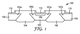
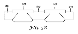
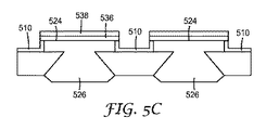
実施形態1は、可撓性LEDアセンブリであって、
可撓性ポリマー基板と、
可撓性基板内及び可撓性基板の表面上に位置付けられた第1の導電性特徴部と、
第1の導電性特徴部から所定の距離において前記可撓性基板内及び可撓性基板の表面上に位置付けられた第2の導電性特徴部であって、前記第1の導電性特徴部と前記第2の導電性特徴部との間に前記可撓性ポリマー基板の一部分が露出されるようになっている、第2の導電性特徴部と、
前記第1の導電性特徴部と前記第2の導電性特徴部との間の前記露出した可撓性ポリマーの表面上に位置付けられる、セラミック層と、を備える、可撓性LEDアセンブリである。
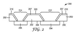
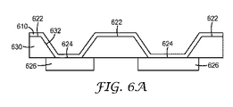
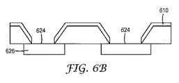
可撓性ポリマー基板を貫通して延在するビアを備える当該可撓性ポリマー基板と、
前記可撓性基板の下面に位置付けられた第1の導電性特徴部であって、前記第1の導電性特徴部の一部分が前記ビアの下に位置付けられている、第1の導電性特徴部と、
前記可撓性ポリマー基板の上面に位置付けられたセラミック層と、を備える、可撓性LEDアセンブリ。
セラミック層を基板の表面に適用する工程であって、前記基板が、前記セラミックの適用前に、露出した上面がポリマーである第1の部分と、前記露出した上面が導電性金属である第2の部分と、を備える、工程と、
前記セラミックを前記基板の表面の前記第2の部分から除去する工程と、
前記基板の表面の前記第2の部分内の前記導電性金属に表面仕上げする工程と、を含む、方法。
Claims (15)
- 可撓性ポリマー基板と、
前記可撓性基板内及び可撓性基板の表面上に位置付けられた第1の導電性特徴部と、
前記第1の導電性特徴部から所定の距離において前記可撓性基板内及び可撓性基板の表面上に位置付けられた第2の導電性特徴部であって、前記第1の導電性特徴部と前記第2の導電性特徴部との間に前記可撓性ポリマー基板の一部分が露出されるようになっている、第2の導電性特徴部と、
前記第1の導電性特徴部と前記第2の導電性特徴部との間の前記露出した可撓性ポリマーの表面上に位置付けられた、セラミック層と、
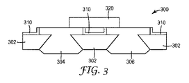
を備える、可撓性LEDアセンブリ。 - 前記第1の導電性特徴部及び前記第2の導電性特徴部の両方に搭載されたLEDを更に備え、前記可撓性ポリマー基板が、前記セラミック層によって前記LEDから放射されるUV光から遮蔽されている、請求項1に記載の可撓性LEDアセンブリ。
- 前記可撓性ポリマー基板がポリイミドを含む、請求項1に記載の可撓性LEDアセンブリ。
- 前記セラミックが、Al2O3、AlN、又はBNを含む、請求項1に記載の可撓性LEDアセンブリ。
- 前記LEDが、前記第1の導電性特徴部及び前記第2の導電性特徴部にはんだ接合されたフリップチップを備える、請求項2に記載の可撓性LEDアセンブリ。
- 前記LEDが前記第1の導電性特徴部及び前記第2の導電性特徴部に共晶接合されている、請求項2に記載の可撓性LEDアセンブリ。
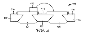
- 前記第2の導電性特徴部ではなく前記第1の導電性特徴部に搭載されたLEDを更に備え、前記可撓性ポリマー基板が前記セラミック層によって、前記LEDから放射されるUV光から遮蔽されている、請求項1に記載の可撓性LEDアセンブリ。
- 前記LEDが、エポキシ結合接着剤、導電性ペースト、異方性導電性ペースト(ACP)、異方性導電性フィルム(ACF)、又は共晶接合を使用して、前記第1の導電性特徴部に取り付けられている、請求項7に記載の可撓性LEDアセンブリ。
- 可撓性ポリマー基板を貫通して延在するビアを備える当該可撓性ポリマー基板と、
前記可撓性基板の下面に位置付けられた第1の導電性特徴部であって、前記第1の導電性特徴部の一部分が前記ビアの下に位置付けられている、第1の導電性特徴部と、
前記可撓性ポリマー基板の上面に位置付けられたセラミック層と、
を備える、可撓性LEDアセンブリ。 - 前記可撓性ポリマー基板内にある第2のビアと、前記可撓性基板の下面に位置付けられた第2の導電性特徴部とを更に備え、前記第2の導電性特徴部の一部分が前記第2のビアの下に位置付けられている、請求項9に記載の可撓性LEDアセンブリ。
- LEDアセンブリを作製する方法であって、
セラミック層を基板の表面に適用する工程であって、前記基板が、前記セラミックの適用前に、露出した上面がポリマーである第1の部分と、前記露出した上面が導電性金属である第2の部分と、を備える、工程と、
前記セラミックを前記基板の表面の前記第2の部分から除去する工程と、
前記基板の表面の前記第2の部分内の前記導電性金属を表面仕上げする工程と、
を含む、方法。 - 前記セラミックを前記基板の表面の前記第2の部分から除去する工程が、粘着性のライナーを前記第2の部分に対応するセラミックの領域上に積層する工程と、前記粘着性のライナーを除去することによって前記セラミックを前記第2の部分から剥離する工程とを含む、請求項11に記載の方法。
- 前記導電性金属を表面仕上げする工程が、最初にニッケル層をめっきし、次に金又は銀の層をめっきする工程を含む、請求項11に記載の方法。
- 前記セラミック層がスパッタリングプロセスを使用して適用される、請求項11に記載の方法。
- 前記セラミックが窒化アルミニウムを含む、請求項11に記載の方法。
Applications Claiming Priority (3)
| Application Number | Priority Date | Filing Date | Title |
|---|---|---|---|
| US201462010224P | 2014-06-10 | 2014-06-10 | |
| US62/010,224 | 2014-06-10 | ||
| PCT/US2015/032363 WO2015191273A1 (en) | 2014-06-10 | 2015-05-26 | Flexible led assembly with uv protection |
Publications (2)
| Publication Number | Publication Date |
|---|---|
| JP2017520915A true JP2017520915A (ja) | 2017-07-27 |
| JP2017520915A5 JP2017520915A5 (ja) | 2018-06-28 |
Family
ID=53366306
Family Applications (1)
| Application Number | Title | Priority Date | Filing Date |
|---|---|---|---|
| JP2016569869A Pending JP2017520915A (ja) | 2014-06-10 | 2015-05-26 | Uv保護を備えた可撓性ledアセンブリ |
Country Status (7)
| Country | Link |
|---|---|
| US (2) | US10121947B2 (ja) |
| EP (1) | EP3155880A1 (ja) |
| JP (1) | JP2017520915A (ja) |
| KR (1) | KR20170019408A (ja) |
| CN (1) | CN106414061B (ja) |
| TW (1) | TW201603310A (ja) |
| WO (1) | WO2015191273A1 (ja) |
Cited By (1)
| Publication number | Priority date | Publication date | Assignee | Title |
|---|---|---|---|---|
| US11362249B2 (en) | 2019-10-11 | 2022-06-14 | Samsung Electronics Co., Ltd. | Display module and manufacturing method thereof |
Families Citing this family (8)
| Publication number | Priority date | Publication date | Assignee | Title |
|---|---|---|---|---|
| JP2017520915A (ja) | 2014-06-10 | 2017-07-27 | スリーエム イノベイティブ プロパティズ カンパニー | Uv保護を備えた可撓性ledアセンブリ |
| KR101802733B1 (ko) * | 2016-05-10 | 2017-11-29 | (주)우주일렉트로닉스 | 차량용 램프 |
| EP3258258A1 (de) * | 2016-06-13 | 2017-12-20 | Airbus Defence and Space GmbH | Sensorhaut |
| JP2018088498A (ja) * | 2016-11-29 | 2018-06-07 | デクセリアルズ株式会社 | 異方性導電接着剤 |
| CN112310115B (zh) * | 2019-07-26 | 2023-06-06 | 京东方科技集团股份有限公司 | 一种驱动背板、显示面板及显示装置 |
| CN110324984B (zh) * | 2019-07-26 | 2020-01-17 | 微智医疗器械有限公司 | 电子元件与电路板的连接方法、电路板组件及电子设备 |
| CN110828647B (zh) * | 2019-11-20 | 2020-12-18 | 深圳市乐的美光电股份有限公司 | 一种柔性led灯串的制造方法 |
| US11837684B2 (en) * | 2019-11-21 | 2023-12-05 | Creeled, Inc. | Submount structures for light emitting diode packages |
Citations (4)
| Publication number | Priority date | Publication date | Assignee | Title |
|---|---|---|---|---|
| JPH11145173A (ja) * | 1997-11-07 | 1999-05-28 | Sony Corp | 半導体装置の製造方法 |
| JP2012151191A (ja) * | 2011-01-17 | 2012-08-09 | Ibiden Co Ltd | Led用配線基板、発光モジュール、led用配線基板の製造方法、及び発光モジュールの製造方法 |
| JP2014017303A (ja) * | 2012-07-06 | 2014-01-30 | Citizen Holdings Co Ltd | Led光源装置及び光反射性基板 |
| JP2015111620A (ja) * | 2013-12-06 | 2015-06-18 | シチズンホールディングス株式会社 | 発光デバイス及びその製造方法 |
Family Cites Families (9)
| Publication number | Priority date | Publication date | Assignee | Title |
|---|---|---|---|---|
| GB2185437B (en) * | 1985-12-26 | 1989-12-06 | Hitachi Chemical Co Ltd | Ceramic coated laminate and process for producing the same |
| JP4290953B2 (ja) * | 2002-09-26 | 2009-07-08 | 奇美電子股▲ふん▼有限公司 | 画像表示装置、有機el素子および画像表示装置の製造方法 |
| AT500259B1 (de) * | 2003-09-09 | 2007-08-15 | Austria Tech & System Tech | Dünnschichtanordnung und verfahren zum herstellen einer solchen dünnschichtanordnung |
| US8171627B2 (en) * | 2007-12-21 | 2012-05-08 | Spansion Llc | Method of forming an electronic device |
| US9179543B2 (en) * | 2010-11-03 | 2015-11-03 | 3M Innovative Properties Company | Flexible LED device with wire bond free die |
| WO2012112873A2 (en) * | 2011-02-18 | 2012-08-23 | 3M Innovative Properties Company | Flexible light emitting semiconductor device |
| EP2490513A2 (en) * | 2011-02-20 | 2012-08-22 | Essence Solar Solutions Ltd. | Light and heat resistant circuit board apparatus and method |
| CN104024723B (zh) * | 2011-11-23 | 2016-08-24 | 3M创新有限公司 | 具有三维结构的柔性发光半导体器件 |
| JP2017520915A (ja) | 2014-06-10 | 2017-07-27 | スリーエム イノベイティブ プロパティズ カンパニー | Uv保護を備えた可撓性ledアセンブリ |
-
2015
- 2015-05-26 JP JP2016569869A patent/JP2017520915A/ja active Pending
- 2015-05-26 KR KR1020177000124A patent/KR20170019408A/ko unknown
- 2015-05-26 WO PCT/US2015/032363 patent/WO2015191273A1/en active Application Filing
- 2015-05-26 EP EP15727807.8A patent/EP3155880A1/en not_active Withdrawn
- 2015-05-26 CN CN201580028138.5A patent/CN106414061B/zh not_active Expired - Fee Related
- 2015-05-26 US US15/316,028 patent/US10121947B2/en not_active Expired - Fee Related
- 2015-06-09 TW TW104118645A patent/TW201603310A/zh unknown
-
2018
- 2018-09-19 US US16/135,317 patent/US10424707B2/en not_active Expired - Fee Related
Patent Citations (4)
| Publication number | Priority date | Publication date | Assignee | Title |
|---|---|---|---|---|
| JPH11145173A (ja) * | 1997-11-07 | 1999-05-28 | Sony Corp | 半導体装置の製造方法 |
| JP2012151191A (ja) * | 2011-01-17 | 2012-08-09 | Ibiden Co Ltd | Led用配線基板、発光モジュール、led用配線基板の製造方法、及び発光モジュールの製造方法 |
| JP2014017303A (ja) * | 2012-07-06 | 2014-01-30 | Citizen Holdings Co Ltd | Led光源装置及び光反射性基板 |
| JP2015111620A (ja) * | 2013-12-06 | 2015-06-18 | シチズンホールディングス株式会社 | 発光デバイス及びその製造方法 |
Cited By (1)
| Publication number | Priority date | Publication date | Assignee | Title |
|---|---|---|---|---|
| US11362249B2 (en) | 2019-10-11 | 2022-06-14 | Samsung Electronics Co., Ltd. | Display module and manufacturing method thereof |
Also Published As
| Publication number | Publication date |
|---|---|
| CN106414061A (zh) | 2017-02-15 |
| US10424707B2 (en) | 2019-09-24 |
| TW201603310A (zh) | 2016-01-16 |
| US20190035993A1 (en) | 2019-01-31 |
| KR20170019408A (ko) | 2017-02-21 |
| US20170104143A1 (en) | 2017-04-13 |
| EP3155880A1 (en) | 2017-04-19 |
| WO2015191273A1 (en) | 2015-12-17 |
| CN106414061B (zh) | 2019-08-16 |
| US10121947B2 (en) | 2018-11-06 |
Similar Documents
| Publication | Publication Date | Title |
|---|---|---|
| US10424707B2 (en) | Flexible LED assembly with UV protection | |
| KR20230014803A (ko) | 연성 회로기판, cof 모듈 및 이를 포함하는 전자 디바이스 | |
| US7119432B2 (en) | Method and apparatus for establishing improved thermal communication between a die and a heatspreader in a semiconductor package | |
| KR101611376B1 (ko) | 칩 온 글라스 본딩 구조체 | |
| US20070178686A1 (en) | Interconnect substrate, semiconductor device, and method of manufacturing the same | |
| JP2008218926A (ja) | 半導体装置及びその製造方法 | |
| US20150223318A1 (en) | Multilayer wiring board | |
| TWI646879B (zh) | 柔性電路板、電路板元件及柔性電路板的製作方法 | |
| TWI736695B (zh) | 電子裝置與其製造方法 | |
| JP2015082576A (ja) | 電子装置、電子機器及び電子装置の製造方法 | |
| TW201344862A (zh) | 具有通孔之球柵陣列封裝基板及其形成方法 | |
| US10014456B2 (en) | Flexible circuits with coplanar conductive features and methods of making same | |
| JP2016219730A (ja) | 電子部品内蔵基板及びその製造方法と電子装置 | |
| KR20070098369A (ko) | 이방성 전도성 페이스트 및 이를 적용한 플라즈마디스플레이 패널 장치 | |
| US20160225706A1 (en) | Printed circuit board, semiconductor package and method of manufacturing the same | |
| US9707706B2 (en) | Flexible substrate embedded with wires and method for fabricating the same | |
| US20170196096A1 (en) | Printed wiring board and method for manufacturing printed wiring board | |
| CN110521292B (zh) | 印刷电路板及其制造方法 | |
| US9281264B2 (en) | Electronic packaging substrate with etching indentation as die attachment anchor and method of manufacturing the same | |
| JP2020004973A5 (ja) | 電子装置 | |
| JPWO2007058108A1 (ja) | 異方導電接着剤 | |
| TWI665773B (zh) | 封裝基板、封裝結構及其製作方法 | |
| US20050005436A1 (en) | Method for preparing thin integrated circuits with multiple circuit layers | |
| KR102105399B1 (ko) | 인쇄회로기판 및 그 제조 방법 | |
| JP2010251764A (ja) | パッケージ材料と基板との間の接着力を高める封止方法 |
Legal Events
| Date | Code | Title | Description |
|---|---|---|---|
| A521 | Request for written amendment filed |
Free format text: JAPANESE INTERMEDIATE CODE: A523 Effective date: 20180517 |
|
| A621 | Written request for application examination |
Free format text: JAPANESE INTERMEDIATE CODE: A621 Effective date: 20180517 |
|
| A977 | Report on retrieval |
Free format text: JAPANESE INTERMEDIATE CODE: A971007 Effective date: 20190313 |
|
| A131 | Notification of reasons for refusal |
Free format text: JAPANESE INTERMEDIATE CODE: A131 Effective date: 20190514 |
|
| RD03 | Notification of appointment of power of attorney |
Free format text: JAPANESE INTERMEDIATE CODE: A7423 Effective date: 20190717 |
|
| A521 | Request for written amendment filed |
Free format text: JAPANESE INTERMEDIATE CODE: A523 Effective date: 20190806 |
|
| RD04 | Notification of resignation of power of attorney |
Free format text: JAPANESE INTERMEDIATE CODE: A7424 Effective date: 20190719 |
|
| A02 | Decision of refusal |
Free format text: JAPANESE INTERMEDIATE CODE: A02 Effective date: 20191105 |