JP2017204510A - Method of manufacturing photoelectric conversion device - Google Patents
Method of manufacturing photoelectric conversion device Download PDFInfo
- Publication number
- JP2017204510A JP2017204510A JP2016094171A JP2016094171A JP2017204510A JP 2017204510 A JP2017204510 A JP 2017204510A JP 2016094171 A JP2016094171 A JP 2016094171A JP 2016094171 A JP2016094171 A JP 2016094171A JP 2017204510 A JP2017204510 A JP 2017204510A
- Authority
- JP
- Japan
- Prior art keywords
- substrate
- photoelectric conversion
- semiconductor layer
- light receiving
- conversion device
- Prior art date
- Legal status (The legal status is an assumption and is not a legal conclusion. Google has not performed a legal analysis and makes no representation as to the accuracy of the status listed.)
- Pending
Links
- 238000006243 chemical reaction Methods 0.000 title claims abstract description 74
- 238000004519 manufacturing process Methods 0.000 title claims abstract description 29
- 239000000758 substrate Substances 0.000 claims abstract description 243
- 239000004065 semiconductor Substances 0.000 claims abstract description 114
- 238000000034 method Methods 0.000 claims description 74
- 239000010410 layer Substances 0.000 description 172
- 239000012212 insulator Substances 0.000 description 26
- 239000011229 interlayer Substances 0.000 description 25
- 238000010586 diagram Methods 0.000 description 14
- 239000012535 impurity Substances 0.000 description 11
- 238000005530 etching Methods 0.000 description 9
- 230000003287 optical effect Effects 0.000 description 9
- 238000009792 diffusion process Methods 0.000 description 8
- 238000012545 processing Methods 0.000 description 8
- RYGMFSIKBFXOCR-UHFFFAOYSA-N Copper Chemical compound [Cu] RYGMFSIKBFXOCR-UHFFFAOYSA-N 0.000 description 7
- 229910052802 copper Inorganic materials 0.000 description 7
- 239000010949 copper Substances 0.000 description 7
- 238000003384 imaging method Methods 0.000 description 7
- 238000002161 passivation Methods 0.000 description 7
- 238000005498 polishing Methods 0.000 description 7
- 238000002955 isolation Methods 0.000 description 6
- 238000012986 modification Methods 0.000 description 5
- 230000004048 modification Effects 0.000 description 5
- 238000001039 wet etching Methods 0.000 description 5
- XUIMIQQOPSSXEZ-UHFFFAOYSA-N Silicon Chemical compound [Si] XUIMIQQOPSSXEZ-UHFFFAOYSA-N 0.000 description 4
- 239000004020 conductor Substances 0.000 description 4
- 230000006870 function Effects 0.000 description 4
- 238000005304 joining Methods 0.000 description 4
- 230000002265 prevention Effects 0.000 description 4
- 230000001681 protective effect Effects 0.000 description 4
- 229910052710 silicon Inorganic materials 0.000 description 4
- 239000010703 silicon Substances 0.000 description 4
- 239000000126 substance Substances 0.000 description 4
- 239000000853 adhesive Substances 0.000 description 3
- 230000001070 adhesive effect Effects 0.000 description 3
- 230000015572 biosynthetic process Effects 0.000 description 3
- 238000001312 dry etching Methods 0.000 description 3
- 230000000149 penetrating effect Effects 0.000 description 3
- 230000002093 peripheral effect Effects 0.000 description 3
- 238000003860 storage Methods 0.000 description 3
- 229910052581 Si3N4 Inorganic materials 0.000 description 2
- 239000003990 capacitor Substances 0.000 description 2
- 239000011521 glass Substances 0.000 description 2
- 238000009413 insulation Methods 0.000 description 2
- 239000000463 material Substances 0.000 description 2
- 238000007747 plating Methods 0.000 description 2
- 239000011347 resin Substances 0.000 description 2
- 229920005989 resin Polymers 0.000 description 2
- 229910021332 silicide Inorganic materials 0.000 description 2
- FVBUAEGBCNSCDD-UHFFFAOYSA-N silicide(4-) Chemical compound [Si-4] FVBUAEGBCNSCDD-UHFFFAOYSA-N 0.000 description 2
- HQVNEWCFYHHQES-UHFFFAOYSA-N silicon nitride Chemical compound N12[Si]34N5[Si]62N3[Si]51N64 HQVNEWCFYHHQES-UHFFFAOYSA-N 0.000 description 2
- 125000006850 spacer group Chemical group 0.000 description 2
- 238000012546 transfer Methods 0.000 description 2
- VYPSYNLAJGMNEJ-UHFFFAOYSA-N Silicium dioxide Chemical compound O=[Si]=O VYPSYNLAJGMNEJ-UHFFFAOYSA-N 0.000 description 1
- 238000005253 cladding Methods 0.000 description 1
- 239000010941 cobalt Substances 0.000 description 1
- 229910017052 cobalt Inorganic materials 0.000 description 1
- GUTLYIVDDKVIGB-UHFFFAOYSA-N cobalt atom Chemical compound [Co] GUTLYIVDDKVIGB-UHFFFAOYSA-N 0.000 description 1
- 238000001514 detection method Methods 0.000 description 1
- 230000009977 dual effect Effects 0.000 description 1
- 238000005516 engineering process Methods 0.000 description 1
- 238000000227 grinding Methods 0.000 description 1
- 238000005286 illumination Methods 0.000 description 1
- 238000010030 laminating Methods 0.000 description 1
- 239000004973 liquid crystal related substance Substances 0.000 description 1
- 238000005259 measurement Methods 0.000 description 1
- 229910021334 nickel silicide Inorganic materials 0.000 description 1
- RUFLMLWJRZAWLJ-UHFFFAOYSA-N nickel silicide Chemical compound [Ni]=[Si]=[Ni] RUFLMLWJRZAWLJ-UHFFFAOYSA-N 0.000 description 1
- 238000004806 packaging method and process Methods 0.000 description 1
- 230000035515 penetration Effects 0.000 description 1
- 238000005375 photometry Methods 0.000 description 1
- 229910052814 silicon oxide Inorganic materials 0.000 description 1
- WFKWXMTUELFFGS-UHFFFAOYSA-N tungsten Chemical compound [W] WFKWXMTUELFFGS-UHFFFAOYSA-N 0.000 description 1
- 239000010937 tungsten Substances 0.000 description 1
- 229910052721 tungsten Inorganic materials 0.000 description 1
Images


Classifications
-
- H—ELECTRICITY
- H01—ELECTRIC ELEMENTS
- H01L—SEMICONDUCTOR DEVICES NOT COVERED BY CLASS H10
- H01L31/00—Semiconductor devices sensitive to infrared radiation, light, electromagnetic radiation of shorter wavelength or corpuscular radiation and specially adapted either for the conversion of the energy of such radiation into electrical energy or for the control of electrical energy by such radiation; Processes or apparatus specially adapted for the manufacture or treatment thereof or of parts thereof; Details thereof
- H01L31/02—Details
- H01L31/0203—Containers; Encapsulations, e.g. encapsulation of photodiodes
-
- H—ELECTRICITY
- H01—ELECTRIC ELEMENTS
- H01L—SEMICONDUCTOR DEVICES NOT COVERED BY CLASS H10
- H01L21/00—Processes or apparatus adapted for the manufacture or treatment of semiconductor or solid state devices or of parts thereof
- H01L21/02—Manufacture or treatment of semiconductor devices or of parts thereof
- H01L21/02104—Forming layers
- H01L21/02365—Forming inorganic semiconducting materials on a substrate
- H01L21/02436—Intermediate layers between substrates and deposited layers
- H01L21/02439—Materials
- H01L21/02491—Conductive materials
-
- H—ELECTRICITY
- H01—ELECTRIC ELEMENTS
- H01L—SEMICONDUCTOR DEVICES NOT COVERED BY CLASS H10
- H01L23/00—Details of semiconductor or other solid state devices
- H01L23/48—Arrangements for conducting electric current to or from the solid state body in operation, e.g. leads, terminal arrangements ; Selection of materials therefor
- H01L23/488—Arrangements for conducting electric current to or from the solid state body in operation, e.g. leads, terminal arrangements ; Selection of materials therefor consisting of soldered or bonded constructions
- H01L23/498—Leads, i.e. metallisations or lead-frames on insulating substrates, e.g. chip carriers
- H01L23/49827—Via connections through the substrates, e.g. pins going through the substrate, coaxial cables
-
- H—ELECTRICITY
- H01—ELECTRIC ELEMENTS
- H01L—SEMICONDUCTOR DEVICES NOT COVERED BY CLASS H10
- H01L27/00—Devices consisting of a plurality of semiconductor or other solid-state components formed in or on a common substrate
- H01L27/14—Devices consisting of a plurality of semiconductor or other solid-state components formed in or on a common substrate including semiconductor components sensitive to infrared radiation, light, electromagnetic radiation of shorter wavelength or corpuscular radiation and specially adapted either for the conversion of the energy of such radiation into electrical energy or for the control of electrical energy by such radiation
- H01L27/144—Devices controlled by radiation
- H01L27/146—Imager structures
- H01L27/14601—Structural or functional details thereof
- H01L27/14625—Optical elements or arrangements associated with the device
- H01L27/14627—Microlenses
-
- H—ELECTRICITY
- H01—ELECTRIC ELEMENTS
- H01L—SEMICONDUCTOR DEVICES NOT COVERED BY CLASS H10
- H01L27/00—Devices consisting of a plurality of semiconductor or other solid-state components formed in or on a common substrate
- H01L27/14—Devices consisting of a plurality of semiconductor or other solid-state components formed in or on a common substrate including semiconductor components sensitive to infrared radiation, light, electromagnetic radiation of shorter wavelength or corpuscular radiation and specially adapted either for the conversion of the energy of such radiation into electrical energy or for the control of electrical energy by such radiation
- H01L27/144—Devices controlled by radiation
- H01L27/146—Imager structures
- H01L27/14601—Structural or functional details thereof
- H01L27/14625—Optical elements or arrangements associated with the device
- H01L27/14629—Reflectors
-
- H—ELECTRICITY
- H01—ELECTRIC ELEMENTS
- H01L—SEMICONDUCTOR DEVICES NOT COVERED BY CLASS H10
- H01L27/00—Devices consisting of a plurality of semiconductor or other solid-state components formed in or on a common substrate
- H01L27/14—Devices consisting of a plurality of semiconductor or other solid-state components formed in or on a common substrate including semiconductor components sensitive to infrared radiation, light, electromagnetic radiation of shorter wavelength or corpuscular radiation and specially adapted either for the conversion of the energy of such radiation into electrical energy or for the control of electrical energy by such radiation
- H01L27/144—Devices controlled by radiation
- H01L27/146—Imager structures
- H01L27/14643—Photodiode arrays; MOS imagers
-
- H—ELECTRICITY
- H01—ELECTRIC ELEMENTS
- H01L—SEMICONDUCTOR DEVICES NOT COVERED BY CLASS H10
- H01L27/00—Devices consisting of a plurality of semiconductor or other solid-state components formed in or on a common substrate
- H01L27/14—Devices consisting of a plurality of semiconductor or other solid-state components formed in or on a common substrate including semiconductor components sensitive to infrared radiation, light, electromagnetic radiation of shorter wavelength or corpuscular radiation and specially adapted either for the conversion of the energy of such radiation into electrical energy or for the control of electrical energy by such radiation
- H01L27/144—Devices controlled by radiation
- H01L27/146—Imager structures
- H01L27/14683—Processes or apparatus peculiar to the manufacture or treatment of these devices or parts thereof
- H01L27/1469—Assemblies, i.e. hybrid integration
-
- H—ELECTRICITY
- H01—ELECTRIC ELEMENTS
- H01L—SEMICONDUCTOR DEVICES NOT COVERED BY CLASS H10
- H01L31/00—Semiconductor devices sensitive to infrared radiation, light, electromagnetic radiation of shorter wavelength or corpuscular radiation and specially adapted either for the conversion of the energy of such radiation into electrical energy or for the control of electrical energy by such radiation; Processes or apparatus specially adapted for the manufacture or treatment thereof or of parts thereof; Details thereof
- H01L31/0248—Semiconductor devices sensitive to infrared radiation, light, electromagnetic radiation of shorter wavelength or corpuscular radiation and specially adapted either for the conversion of the energy of such radiation into electrical energy or for the control of electrical energy by such radiation; Processes or apparatus specially adapted for the manufacture or treatment thereof or of parts thereof; Details thereof characterised by their semiconductor bodies
- H01L31/0256—Semiconductor devices sensitive to infrared radiation, light, electromagnetic radiation of shorter wavelength or corpuscular radiation and specially adapted either for the conversion of the energy of such radiation into electrical energy or for the control of electrical energy by such radiation; Processes or apparatus specially adapted for the manufacture or treatment thereof or of parts thereof; Details thereof characterised by their semiconductor bodies characterised by the material
- H01L31/0264—Inorganic materials
-
- H—ELECTRICITY
- H01—ELECTRIC ELEMENTS
- H01L—SEMICONDUCTOR DEVICES NOT COVERED BY CLASS H10
- H01L31/00—Semiconductor devices sensitive to infrared radiation, light, electromagnetic radiation of shorter wavelength or corpuscular radiation and specially adapted either for the conversion of the energy of such radiation into electrical energy or for the control of electrical energy by such radiation; Processes or apparatus specially adapted for the manufacture or treatment thereof or of parts thereof; Details thereof
- H01L31/04—Semiconductor devices sensitive to infrared radiation, light, electromagnetic radiation of shorter wavelength or corpuscular radiation and specially adapted either for the conversion of the energy of such radiation into electrical energy or for the control of electrical energy by such radiation; Processes or apparatus specially adapted for the manufacture or treatment thereof or of parts thereof; Details thereof adapted as photovoltaic [PV] conversion devices
-
- H—ELECTRICITY
- H01—ELECTRIC ELEMENTS
- H01L—SEMICONDUCTOR DEVICES NOT COVERED BY CLASS H10
- H01L31/00—Semiconductor devices sensitive to infrared radiation, light, electromagnetic radiation of shorter wavelength or corpuscular radiation and specially adapted either for the conversion of the energy of such radiation into electrical energy or for the control of electrical energy by such radiation; Processes or apparatus specially adapted for the manufacture or treatment thereof or of parts thereof; Details thereof
- H01L31/18—Processes or apparatus specially adapted for the manufacture or treatment of these devices or of parts thereof
- H01L31/1876—Particular processes or apparatus for batch treatment of the devices
-
- H—ELECTRICITY
- H01—ELECTRIC ELEMENTS
- H01L—SEMICONDUCTOR DEVICES NOT COVERED BY CLASS H10
- H01L31/00—Semiconductor devices sensitive to infrared radiation, light, electromagnetic radiation of shorter wavelength or corpuscular radiation and specially adapted either for the conversion of the energy of such radiation into electrical energy or for the control of electrical energy by such radiation; Processes or apparatus specially adapted for the manufacture or treatment thereof or of parts thereof; Details thereof
- H01L31/18—Processes or apparatus specially adapted for the manufacture or treatment of these devices or of parts thereof
- H01L31/1892—Processes or apparatus specially adapted for the manufacture or treatment of these devices or of parts thereof methods involving the use of temporary, removable substrates
-
- H—ELECTRICITY
- H01—ELECTRIC ELEMENTS
- H01L—SEMICONDUCTOR DEVICES NOT COVERED BY CLASS H10
- H01L31/00—Semiconductor devices sensitive to infrared radiation, light, electromagnetic radiation of shorter wavelength or corpuscular radiation and specially adapted either for the conversion of the energy of such radiation into electrical energy or for the control of electrical energy by such radiation; Processes or apparatus specially adapted for the manufacture or treatment thereof or of parts thereof; Details thereof
- H01L31/18—Processes or apparatus specially adapted for the manufacture or treatment of these devices or of parts thereof
- H01L31/20—Processes or apparatus specially adapted for the manufacture or treatment of these devices or of parts thereof such devices or parts thereof comprising amorphous semiconductor materials
-
- H—ELECTRICITY
- H01—ELECTRIC ELEMENTS
- H01L—SEMICONDUCTOR DEVICES NOT COVERED BY CLASS H10
- H01L27/00—Devices consisting of a plurality of semiconductor or other solid-state components formed in or on a common substrate
- H01L27/14—Devices consisting of a plurality of semiconductor or other solid-state components formed in or on a common substrate including semiconductor components sensitive to infrared radiation, light, electromagnetic radiation of shorter wavelength or corpuscular radiation and specially adapted either for the conversion of the energy of such radiation into electrical energy or for the control of electrical energy by such radiation
- H01L27/144—Devices controlled by radiation
- H01L27/146—Imager structures
- H01L27/14601—Structural or functional details thereof
- H01L27/1462—Coatings
- H01L27/14621—Colour filter arrangements
-
- H—ELECTRICITY
- H01—ELECTRIC ELEMENTS
- H01L—SEMICONDUCTOR DEVICES NOT COVERED BY CLASS H10
- H01L27/00—Devices consisting of a plurality of semiconductor or other solid-state components formed in or on a common substrate
- H01L27/14—Devices consisting of a plurality of semiconductor or other solid-state components formed in or on a common substrate including semiconductor components sensitive to infrared radiation, light, electromagnetic radiation of shorter wavelength or corpuscular radiation and specially adapted either for the conversion of the energy of such radiation into electrical energy or for the control of electrical energy by such radiation
- H01L27/144—Devices controlled by radiation
- H01L27/146—Imager structures
- H01L27/14601—Structural or functional details thereof
- H01L27/14634—Assemblies, i.e. Hybrid structures
-
- Y—GENERAL TAGGING OF NEW TECHNOLOGICAL DEVELOPMENTS; GENERAL TAGGING OF CROSS-SECTIONAL TECHNOLOGIES SPANNING OVER SEVERAL SECTIONS OF THE IPC; TECHNICAL SUBJECTS COVERED BY FORMER USPC CROSS-REFERENCE ART COLLECTIONS [XRACs] AND DIGESTS
- Y02—TECHNOLOGIES OR APPLICATIONS FOR MITIGATION OR ADAPTATION AGAINST CLIMATE CHANGE
- Y02E—REDUCTION OF GREENHOUSE GAS [GHG] EMISSIONS, RELATED TO ENERGY GENERATION, TRANSMISSION OR DISTRIBUTION
- Y02E10/00—Energy generation through renewable energy sources
- Y02E10/50—Photovoltaic [PV] energy
Abstract
Description
本発明は、光電変換装置に関する。 The present invention relates to a photoelectric conversion device.
光電変換素子が設けられた受光基板と、半導体素子が設けられた回路基板と、を積層した光電変換装置が提案されている。複数の基板を積層することにより、光電変換装置の性能の向上が期待される。 There has been proposed a photoelectric conversion device in which a light-receiving substrate provided with a photoelectric conversion element and a circuit board provided with a semiconductor element are stacked. By laminating a plurality of substrates, an improvement in the performance of the photoelectric conversion device is expected.
特許文献1には、光電変換素子を有する第1の基板と、周辺回路部を有する第2の基板とを積層した、裏面照射型の固体撮像装置が開示されている。
複数の基板を積層すると光電変換装置が厚くなってしまうため、基板を薄くする要求がある。特許文献1ではフォトダイオード形成部材の薄膜化を行っているが、薄膜化によって新たに形成される面が受光面となるため、薄膜化に起因したノイズが生じやすい。そのため、光電変換装置の性能の向上が十分ではないという課題があった。
When a plurality of substrates are stacked, the photoelectric conversion device becomes thick, and thus there is a demand for thinning the substrate. In
本発明は、光電変換装置の性能を向上することを目的とする。 An object of this invention is to improve the performance of a photoelectric conversion apparatus.
上記課題を解決するための手段の一つの観点は、光電変換素子が設けられた半導体層を含む第1基板を、第2基板に固定する工程と、前記第2基板に固定された前記第1基板を、前記第1基板に対して前記第2基板の側とは反対側から薄化する工程と、前記薄化された第1基板を、半導体素子が設けられた第3基板が前記第1基板に対して前記第2基板の側とは反対側に位置するように、前記第3基板に固定する工程と、前記第1基板を前記第3基板に固定する工程の後に、前記第2基板を除去する工程と、を備えることを特徴とする光電変換装置の製造方法である。 One aspect of the means for solving the above problems is a step of fixing a first substrate including a semiconductor layer provided with a photoelectric conversion element to a second substrate, and the first substrate fixed to the second substrate. A step of thinning the substrate from the side opposite to the second substrate side with respect to the first substrate; and the thinned first substrate is a third substrate provided with a semiconductor element. After the step of fixing to the third substrate and the step of fixing the first substrate to the third substrate so as to be located on the opposite side of the substrate from the second substrate side, the second substrate And a step of removing the photoelectric conversion device.
本発明によれば、性能を向上した光電変換装置を提供することができる。 According to the present invention, a photoelectric conversion device with improved performance can be provided.
以下、図面を参照して、本発明を実施するための形態を説明する。なお、以下の説明および図面において、複数の図面に渡って共通の構成については共通の符号を付している。そして、共通する構成を断りなく複数の図面を相互に参照して説明する場合がる。また、共通の符号を付した構成については説明を省略する場合がある。 Hereinafter, embodiments for carrying out the present invention will be described with reference to the drawings. Note that, in the following description and drawings, common reference numerals are given to common configurations over a plurality of drawings. In some cases, a common configuration may be described with reference to a plurality of drawings without reference. In addition, description of the components with common reference numerals may be omitted.
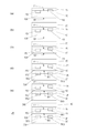
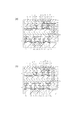
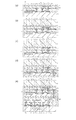
図1では、光電変換装置の断面模式図を用いて光電変換装置の製造方法を工程順に示している。 In FIG. 1, the manufacturing method of a photoelectric conversion device is illustrated in the order of steps using a schematic cross-sectional view of the photoelectric conversion device.
図1(a)に示す工程Aでは、光電変換素子PDが設けられた受光基板10を用意する。受光基板10には光電変換素子PD以外に半導体素子TR1が設けられていてもよい。受光基板10は光電変換素子PDや半導体素子TR1の少なくとも一部を含む半導体層100を有する。工程Aにおいて半導体層100は表面F1と裏面B1とを有する。受光基板10における表面F1は最終的な光電変換装置における半導体層100の受光面となる。なお、受光基板10の裏面は半導体層100の裏面B1に一致しうるが、受光基板10の裏面が半導体層100以外の層で構成されていてもよい。半導体素子TR1は例えばn型のMOSトランジスタである。半導体素子TR1は光電変換素子PDと共に画素回路を構成しうる。受光基板10は半導体層100の上に設けられた第1配線部材15を含むことができる。第1配線部材15は、半導体装置で一般的に用いられる配線構造(多層配線構造)の複数の構成要素の少なくともいずれかを含みうる。配線構造(多層配線構造)の複数の構成要素とは、コンタクトプラグ、配線層、ビアプラグ、コンタクトプラグ用や配線層用のエッチングストップ層、層間絶縁層、配線層の拡散防止層、およびパッシベーション層である。受光基板10は第1配線部材15を含まなくてもよい。
In step A shown in FIG. 1A, a light receiving
図1(b)に示す工程Bでは、光電変換素子PDが設けられた受光基板10を支持基板20に固定する。工程Bにおいて、受光基板10が第1配線部材15を含む場合には、第1配線部材15が半導体層100と支持基板20との間に位置する。
In step B shown in FIG. 1B, the
図1(c)に示す工程Cでは、支持基板20に固定された受光基板10を、受光基板10に対して支持基板20の側とは反対側(裏面B1側)から薄化する。半導体層100の薄化とは半導体層100の厚さを小さくすることである。薄化においては、受光基板10のうち、受光基板10の支持基板20の側とは反対側の面(裏面B1)を含む部分が除去される。工程Cにおける半導体層100の薄化によって、半導体層100には新たな裏面B2が形成される。
In step C shown in FIG. 1C, the
図1(d)に示す工程Dでは、薄化された受光基板10を、半導体素子TR2が設けられた回路基板30に固定する。この固定は、回路基板30が受光基板10に対して支持基板20の側とは反対側(裏面B2側)に位置するように行われる。回路基板30には半導体素子TR2以外に半導体素子TR3が設けられていてもよい。回路基板30は半導体素子TR2や半導体素子TR3の少なくとも一部を含む半導体層300を有する。半導体素子TR2は例えばn型のMOSトランジスタであり、半導体素子TR3は例えばp型のMOSトランジスタである。半導体素子TR2と半導体素子TR3は共にアナログ信号処理回路やデジタル信号処理回路、AD変換回路あるいは駆動回路を構成しうる。回路基板30には光電変換素子が設けられていてもよい。回路基板30に設けられた光電変換素子は、受光基板10を透過した光を受光することができる。
In step D shown in FIG. 1D, the thinned
回路基板30は半導体層300の上に設けられた第2配線部材35を含むことができる。第2配線部材35は、第1配線部材15と同様に半導体装置で一般的に用いられる配線構造(多層配線構造)における構成要素の少なくともいずれかを含みうる。回路基板30は第2配線部材35を含まなくてもよい。図1(d)に示すように、工程Dにおいて、回路基板30が第2配線部材35を含む場合には、第2配線部材35が半導体層300と受光基板10との間に位置しうる。これに限らず、半導体層300が第2配線部材35と受光基板10との間に位置するように、回路基板30を配置することもできる。
The
図1(e)に示す工程Eでは、回路基板30に固定された受光基板10の上から支持基板20を除去する。支持基板20は完全に除去することが好ましいが、支持基板20の少なくとも一部が除去されればよく、受光に影響を与えない範囲で支持基板20の一部が受光基板10の上に残っていてもよい。
In step E shown in FIG. 1E, the
図1(f)示す工程Fでは、支持基板20を除去する工程Eの後に、受光基板10に対して回路基板30の側とは反対側(表面F1側)に光学部材40を形成する。光学部材40はトップレンズ(マイクロレンズ)や層内レンズなどの集光部、カラーフィルタなどの波長選択部、およびコアクラッド構造を有する導光部(導光路、光導波路とも言う)、遮光部の少なくともいずれかを含みうる。
In the process F shown in FIG. 1F, after the process E of removing the
なお、工程Bにおいて受光基板10が第1配線部材15を含まない場合には、工程Eと工程Fとの間に、第1配線部材15に相当する配線部材を形成してもよい。工程Aで第1配線部材15の一部を形成し、工程Eと工程Fとの間に第1配線部材15の残りの一部を形成してもよい。
When the
この後、受光基板10と回路基板30の積層体をダイシングして、複数基板を積層したチップを得ることができる。チップはパッケージングされる。
Thereafter, the stacked body of the
本実施形態によれば、受光基板10を薄化することにより回路基板30を設けても光電変換装置の厚みの増加を抑制できる。
According to this embodiment, even if the
また、本実施形態によれば、支持基板20とは反対側の面から受光基板10を薄化し、支持基板20側の面を受光面として用いることができるため、薄化に伴って生じ得るノイズを低減することができる。
Further, according to the present embodiment, since the
また、本実施形態によれば、支持基板20を除去することにより、支持基板20による半導体層100への入射光の減衰を抑制できる。
In addition, according to the present embodiment, by removing the
また、本実施形態によれば、光学部材40を支持基板20の除去後に形成することで、光学部材40が、支持基板20の着脱時(工程B.E)や受光基板10の薄化時(工程C)に損傷することを避けることができる。よって、光学特性に優れた光電変換装置を得ることができる。同様に、第1配線部材15の少なくとも一部を支持基板20の除去後に形成すれば、第1配線部材15の損傷を低減することができる。そのため、電気的特性や信頼性に優れた光電変換装置を得ることができる。このように、受光面上に配されることになる部材の少なくとも一部を、薄化する工程Cの前ではなく、支持基板20を除去する工程Eの後に行うことで、受光面上に配される部材に、薄化時や支持基板20の固定時あるいは除去時に生じるダメージを低減することできる。よって、信頼性の高い光電変換装置を製造することができ、また、歩留まり良く光電変換装置を製造することができる。
Further, according to the present embodiment, the
受光基板10と回路基板30は電気的に相互接続される。この電気的接続は、チップの外でワイヤボンディング接続やフリップチップ接続によって実現することができる。あるいは、受光基板10と回路基板30との接続を、チップ内で半導体層100および/または半導体層300を貫通する導電部材である貫通電極によって実現することができる。貫通電極の形成には、スルーシリコンビア(TSV)技術を用いることができる。
The
貫通電極の形成は、導電部材の形成と、導電部材による半導体層の貫通の実現の2つに分けて考えることができる。貫通電極の形成の第1例では、工程Cの後に、受光基板10に対して支持基板20とは反対側から、受光基板10の半導体層100に貫通孔を形成する。そして、貫通孔内に導電部材を形成する。これにより、半導体層100を貫通する導電部材である貫通電極を形成する。その後に、回路基板30が貫通電極に接続するように工程Dを行う。
Formation of the through electrode can be considered in two ways: formation of a conductive member and realization of penetration of the semiconductor layer by the conductive member. In the first example of the formation of the through electrode, after step C, a through hole is formed in the
貫通電極の形成の第2例では、工程Eの後に、受光基板10に対して回路基板30とは反対側から、受光基板10の半導体層100に貫通孔を、形成する。そして、貫通孔内に導電部材を形成する。これにより、半導体層100を貫通する導電部材である貫通電極を形成する。貫通孔を回路基板30に達するように形成することで、半導体層100を貫通する導電部材を回路基板30に接続できる。
In the second example of forming the through electrode, after step E, a through hole is formed in the
貫通電極の形成の第3例では、工程Bの前に、受光基板10の半導体層100に孔を形成する。そして、この孔の中に導電部材を形成する。そして、工程Cで、受光基板10に対して支持基板20側とは反対側に導電部材を露出させる。これにより、半導体層100を貫通する導電部材である貫通電極を形成する。支持基板20側とは反対側に露出した導電部材を回路基板30に接続できる。
In the third example of forming the through electrode, a hole is formed in the
ウエハレベルチップサイズパッケージ(WLCSP)型の光電変換装置を製造することもできる。WLCSP型の光電変換装置では、受光基板10と回路基板30の積層体のダイシング前にガラスウエハなどの透光基板(不図示)に受光基板10と回路基板30の積層体を接着する。このとき、透光基板と回路基板30との間に受光基板10が位置することになる。そして、透光基板と受光基板10と回路基板30とを併せてダイシングする。これにより、透光基板、受光基板、回路基板がこの順で積層された光電変換装置を得ることができる。
A wafer level chip size package (WLCSP) type photoelectric conversion device can also be manufactured. In the WLCSP type photoelectric conversion device, the laminated body of the
また、チップオンボード(COB)型の光電変換装置を製造することもできる。COB型の光電変換装置では、配線基板に受光基板10と回路基板30の積層体を接続する。このとき、受光基板10と配線基板との間に回路基板30が位置することになる。そして、受光基板10と回路基板30と配線基板を併せてダイシングする。これにより、受光基板、回路基板、配線基板がこの順で積層された光電変換装置を得ることができる。もちろん、WLCSP型とCOB型を組み合わせて、透光基板、受光基板、回路基板、配線基板がこの順で積層された光電変換装置を得ることもできる。
A chip-on-board (COB) type photoelectric conversion device can also be manufactured. In a COB type photoelectric conversion device, a laminate of a
以上説明した光電変換装置は、カメラに用いられる撮像装置(イメージセンサ)として使用できる。この他、焦点検出(AF:オートフォーカス)用のセンサや測光(AE:オートエクスポージャー)用のセンサ、測距用のセンサにも適用できる。 The photoelectric conversion device described above can be used as an imaging device (image sensor) used for a camera. In addition, the present invention can be applied to a sensor for focus detection (AF: autofocus), a sensor for photometry (AE: auto exposure), and a sensor for distance measurement.
カメラは、撮像装置としての光電変換装置以外に、信号処理装置、記憶装置、表示装置および光学装置の少なくともいずれかを備えることができる。信号処理装置は、例えばCPUやDSPであり、撮像装置から得られた信号を処理する。記憶装置は、例えばDRAMやフラッシュメモリであり、撮像装置から得られた信号に基づく情報を記憶する。表示装置は、例えば液晶ディスプレイや有機ELディスプレイであり、撮像装置で得られた信号に基づく情報を表示する。光学装置は、例えばレンズやミラー、シャッター、フィルタであり、撮像装置へ光を導く。ここでいうカメラとはスチルカメラやビデオカメラ、監視カメラ等のカメラ専用機器以外に、撮影機能を有する情報端末や撮影機能を有する移動体(車両や飛行体)も包含する。 The camera can include at least one of a signal processing device, a storage device, a display device, and an optical device in addition to the photoelectric conversion device as the imaging device. The signal processing device is, for example, a CPU or a DSP, and processes a signal obtained from the imaging device. The storage device is, for example, a DRAM or a flash memory, and stores information based on a signal obtained from the imaging device. The display device is a liquid crystal display or an organic EL display, for example, and displays information based on a signal obtained by the imaging device. The optical device is, for example, a lens, a mirror, a shutter, or a filter, and guides light to the imaging device. In addition to camera-dedicated equipment such as a still camera, a video camera, and a surveillance camera, the camera here includes an information terminal having a photographing function and a moving body (vehicle or flying object) having a photographing function.
以下、実施例1〜3を挙げて、詳細に説明する。なお実施例1〜3で重複する事項は説名を省略する。 Hereinafter, examples 1 to 3 will be described in detail. In addition, the description name is abbreviate | omitted about the matter which overlaps in Examples 1-3.
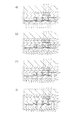
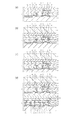
図2(a)〜(c)に示す工程は、図1で説明した工程Aに相当する。 The steps shown in FIGS. 2A to 2C correspond to the step A described with reference to FIG.
図2(a)に示すように、半導体層100を有する半導体ウエハを用意する。
As shown in FIG. 2A, a semiconductor wafer having a
図2(b)に示す工程では、半導体層100の素子部(活性部)を画定する素子分離部101を形成する。ここで、素子分離部101は酸化シリコン膜等のフィールド絶縁膜によって構成され、LOCOS、STIの何れの方法で形成しても良い。そして、半導体層100にフォトダイオードである光電変換素子PDやトランジスタである半導体素子TR1を形成する。半導体素子TR1は、MOS構造を有するゲート111、サイドスペーサ112、ソース、ドレインの不純物領域113を有する。ウェル、ゲート絶縁膜及びLDD用の不純物領域については図が細かくなる為、敢えて図示していない。フォトダイオードである光電変換素子PDは、電荷蓄積領域であるn型の不純物領域121と、その周囲のp型の不純物領域を含む。さらに、不純物領域121と半導体層100の表面との間にはp型の不純物領域122が設けられており、これによって、光電変換素子PDは埋め込み型フォトダイオードとなっている。転送ゲート123は浮遊拡散領域(フローティングディフュージョン)であるn型の不純物領域124に電荷(電子)を転送する。
In the step shown in FIG. 2B, an element isolation portion 101 that defines an element portion (active portion) of the
図2(c)に示す工程では、受光基板10を形成する。受光基板10は半導体層100の上に配線部材を有する。配線部材は、層間絶縁層130、層間絶縁層130を貫通するコンタクトプラグ131を含む。配線部材は、さらに、第1配線層132、第1配線層132上の層間絶縁層140、第1配線層132と第2配線層142の間の第1ビアプラグ141、第2配線層142を含む。配線部材は、さらに、第2配線層142上の層間絶縁層150、第2配線層142と第3配線層152の間の第2ビアプラグ151、第3配線層152、第3配線層152上のパッシベーション膜としての絶縁体膜160を含む。このように、受光基板10には、第3配線層152上のパッシベーション膜としての絶縁体膜160まで設けられている。以上のようにして受光基板10が用意される。
In the step shown in FIG. 2C, the
図2(d)、(e)に示す工程は、図1で説明した工程Bに相当する。図2(d)は、パッシベーション膜としての絶縁体膜160まで形成した受光基板10と支持基板20の接合前の状態を示している。図2(e)は、受光基板10と支持基板20の接合後の状態を示している。受光基板10と支持基板20の接合方法は直接接合あるいは各種接着剤を用いた何れの方法でも構わない。支持基板20はシリコンウエハでもよいし、ガラスウエハでもよいが、熱膨張率の違いによる反りを考慮すると、受光基板10がシリコンウエハであれば、支持基板20もシリコンウエハであることが好ましい。
The steps shown in FIGS. 2D and 2E correspond to the step B described in FIG. FIG. 2D shows a state before bonding of the
図3(f)は、図1で説明した工程Cに相当する。受光基板10をバックグラインド(BG)、化学機械研磨(CMP)、および/またはウェットエッチングにより受光基板10を薄化した状態を表わしている。詳細には、受光基板10の半導体層100の一部が除去され、半導体層100が薄くなる。この時、半導体層100の厚さは薄い方が後の貫通電極用の孔を形成する際のエッチング工程で有利である。一方、半導体層100が薄過ぎるとフォトダイオード特性に影響がある。薄化後の半導体層100の厚さは、5μm以上であることが好ましく、10μmより大きいことがより好ましい。また、薄化後の半導体層100の厚さは、100μmより小さいことが好ましく、50μm以下であることがより好ましい。薄化によって現れる半導体層100の裏面と受光面となる表面との距離が10μmより大きければ、裏面の近傍で生じるノイズの影響を低減できる。
FIG. 3F corresponds to the process C described in FIG. This shows a state in which the
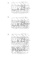
図3(g)〜(k)は、貫通電極を形成する工程を示す。 3G to 3K show a process of forming the through electrode.
図3(g)は受光基板10の薄化後、裏面(研磨面)に絶縁膜180を形成する工程を示している。
FIG. 3G shows a process of forming the insulating
図3(h)は、半導体層100に貫通孔181を形成する工程を示している。貫通孔181は、受光基板10の裏面にレジストを塗布し、レジストの露光、現像を行なってマスクを形成する。マスクを用いて半導体層100をドライエッチングすることにより第1配線層132の接続電極135に達する貫通孔181を形成する。なお、貫通孔181が接続電極135に達するために、半導体層100のエッチングに続いて、素子分離部101のフィールド絶縁膜や層間絶縁層130もエッチングする。図3(h)は、貫通孔181の形成後に、レジストマスクを除去した状態を示している。
FIG. 3H shows a process of forming the through hole 181 in the
図3(i)は、貫通孔181の内面および半導体層100の裏面上に絶縁膜182を形成した状態を示している。
FIG. 3I shows a state in which an insulating film 182 is formed on the inner surface of the through hole 181 and the back surface of the
図4(j)は、絶縁膜182のうち、貫通孔181の底(接続電極135上)に位置する部分を、異方性エッチングにより除去した状態を示している。なお、絶縁膜182のうち、半導体層100の裏面上に位置する部分も除去される。これらの工程は、後に貫通孔181に埋め込む導電部材と半導体層100との絶縁及び、接続電極135との導通を実現する為に行なわれる。
FIG. 4J shows a state where a portion of the insulating film 182 located on the bottom of the through hole 181 (on the connection electrode 135) is removed by anisotropic etching. Note that the portion of the insulating film 182 located on the back surface of the
図4(k)は、貫通孔181の中に導電部材183を埋め込む工程を示している。導電部材183は、銅シード層および銅メッキ層の形成により導電材料を形成し、CMPにより貫通孔181外の余分な導電材料を除去することにより形成できる。
FIG. 4K shows a process of embedding the
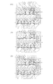
図4(l)、図5(m)は、図1で説明した工程Dに相当する。続く図4(l)では受光基板10と、別途用意した回路基板30の接合前の状態を示している。回路基板30は半導体層300を含む。半導体層300にはトランジスタである半導体素子TR2、TR3、TR4をはじめとして、抵抗素子、容量素子などの各種の半導体素子が形成されている。回路基板30には半導体集積回路として画素回路以外の回路である周辺回路が設けられている。周辺回路は、画素回路を駆動する駆動回路や画素回路からのアナログ信号を処理するアナログ信号処理回路や、アナログ信号をデジタル信号に変換するAD変換回路、デジタル信号を処理するデジタル信号処理回路を含みうる。半導体素子TR2、TR3、TR4はMOS構造を有するゲート311、サイドスペーサ312、ソース、ドレインの不純物領域313、314、315を有する。半導体素子TR3はn型のウェル310に配されている。なお、ゲート絶縁膜は図示を省略している。半導体素子TR2、TR3、TR4はLDD用の不純物領域やHALO用の不純物領域を設けることができるが、図示を省略している。また、半導体素子TR2、TR3、TR4のゲート、ソース、ドレインにはサリサイドプロセスにより、コバルトシリサイドやニッケルシリサイドを包含するシリサイド層が設けることができるが、これも図示を省略している。
4L and 5M correspond to the process D described in FIG. FIG. 4L shows a state before the
半導体層300の上には配線部材が形成されている。配線部材は、コンタクトプラグ331、第1配線層332、ビアプラグ341、第2配線層342、ビアプラグ351、第3配線層352含む。また、これらの配線層間には、層間絶縁層330、340、350が配されている。配線部材には、ダマシン構造を有する銅配線を用いることができる。パッシベーション膜としての絶縁体膜360も設けられている。最上層の配線層である第3配線層352に含まれる接続電極355が露出した状態にある。
A wiring member is formed on the
図5(m)は、パッシベーション膜としての絶縁体膜360まで形成した回路基板30と受光基板10の受光基板10と支持基板20の接合後の状態を示している。受光基板10と回路基板30の接合方法は直接接合あるいは各種接着剤を用いた何れの方法でも構わない。受光基板10の裏面と、回路基板30の表面を接合(貼り合わせる)する事により、受光基板01の第1配線層132の接続電極と回路基板30の接続電極355が導電部材183を通して導通する。
FIG. 5M shows a state after bonding of the
図5(n)は、図1で説明した工程Eに相当する。支持基板20を受光基板10から除去する。支持基板20除去方法は剥離でも、機械研磨、機械化学研磨、ウェットエッチング、剥離の何れの方法でも構わない。
FIG. 5N corresponds to the process E described in FIG. The
図5(o)は、図1で説明した工程Fに相当する。カラーフィルタ191、マイクロレンズ192を形成し、さらに絶縁体膜160もパッド開口193を形成する。その後、ウエハをダイシングしてチップを得て、必要に応じてパッケージングを行う。 FIG. 5O corresponds to the process F described with reference to FIG. A color filter 191 and a microlens 192 are formed, and the insulator film 160 also forms a pad opening 193. Thereafter, the wafer is diced to obtain chips, and packaging is performed as necessary.
これにより、受光基板10と回路基板30を積層した、表面照射型(FSI)の光電変換装置が完成する。
As a result, a front-illuminated (FSI) photoelectric conversion device in which the
実施例1では貫通電極が回路基板30の接続電極355から第1配線層132までとなるので、エッチング対象が、絶縁膜180、半導体層100、素子分離部101フィールド絶縁膜、層間絶縁層130と、少なくて済む。このことは貫通孔181を良好に形成する上で有利である。
In the first embodiment, since the through electrode extends from the connection electrode 355 of the
実施例1では第1配線層132に含まれる接続電極135に導電部材183を接続したが、貫通孔181の加工が可能であれば、どの配線層に含まれる接続電極と接続しても構わない。
In the first embodiment, the
図6(a)は実施例1の第1変形例を示している。第1変形例では導電部材183が第2配線層142に含まれる接続電極145に接続されている。
FIG. 6A shows a first modification of the first embodiment. In the first modification, the
図6(b)は実施例1の第2変形例を示している。第2変形例では導電部材183が第3配線層152に含まれる接続電極155に接続されている。
FIG. 6B shows a second modification of the first embodiment. In the second modification, the
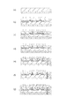
図7(a)に示す工程は、図1で説明した工程Aに相当する。受光基板10には、ビアプラグ151と絶縁体膜160までが形成されている。実施例1とは第3配線層152が形成されていない点が相違する。
The process shown in FIG. 7A corresponds to the process A described in FIG. On the
図7(b)に示す工程は、図1で説明した工程Bに相当する。受光基板10に支持基板20を貼り合わせ、相互に固定する。
The process shown in FIG. 7B corresponds to the process B described in FIG. The
図7(c)に示す工程は、図1で説明した工程Cに相当する。受光基板10を機械研磨(MP)、化学機械研磨(CMP)、あるいはウェットエッチングにより薄化する。
The process shown in FIG. 7C corresponds to the process C described in FIG. The
図7(d)に示す工程は、図1で説明した工程Dに相当する。実施例2においては、回路基板30の接続電極355は絶縁膜380で覆われている。絶縁膜380は受光基板10と回路基板30との接合の前に回路基板30に設けられている。なお、本例では実施例1における絶縁膜180に相当する絶縁膜を省略して、絶縁膜380と半導体層100が接するようにしている。半導体層100の上に絶縁膜180を設けて、絶縁膜180と絶縁膜380とが直接接合するあるいは、接着剤を介して接合するようにしてもよい。
The process shown in FIG. 7D corresponds to the process D described in FIG. In the second embodiment, the connection electrode 355 of the
図8(e)に示す工程は、図1で説明した工程Eに相当する。支持基板20は受光基板10の上から除去されている。
The process shown in FIG. 8E corresponds to the process E described in FIG. The
図8(f)〜図9(h)に示す工程は、貫通電極を形成する工程である。 The process shown in FIGS. 8F to 9H is a process for forming a through electrode.
図8(f)に示す工程では、受光基板10に対して回路基板30とは反対側から、半導体層100を貫通する貫通孔381を形成する。
In the step shown in FIG. 8F, a through hole 381 that penetrates the
貫通孔381は、受光基板10の裏面にレジストを塗布し、レジストの露光、現像を行なってマスクを形成する。マスクを用いて半導体層100をドライエッチングすることにより第3配線層352の接続電極355に達する貫通孔381を形成する。なお、半導体層100のエッチングの前に、絶縁体膜160、層間絶縁層150、140、130および素子分離部101のフィールド絶縁膜もエッチングする。また、貫通孔381が接続電極355に達するために、半導体層100のエッチングの後に、絶縁膜380もエッチングする。
The through hole 381 forms a mask by applying a resist to the back surface of the
また、絶縁体膜160には凹部383を形成する。凹部は絶縁体膜160のエッチングによって形成できる。凹部383と貫通孔381はどちらを先に形成してもかまわない。さらに、貫通孔381および凹部383の内面に絶縁膜382を形成する。 Further, a recess 383 is formed in the insulator film 160. The recess can be formed by etching the insulator film 160. Either the concave portion 383 or the through hole 381 may be formed first. Further, an insulating film 382 is formed on the inner surfaces of the through hole 381 and the recess 383.
図8(g)に示す工程では、絶縁膜382のうち、貫通孔381の底(接続電極355上)に位置する部分と、ビアプラグ151上に位置する部分とを、異方性エッチングにより除去した状態を示している。なお、絶縁膜382のうち、絶縁体膜160に位置する部分も除去される。これらの工程は、後に貫通孔381に埋め込む導電部材と半導体層100との絶縁と、ビアプラグ151や接続電極355との導通を実現する為に行なわれる。
In the step shown in FIG. 8G, the portion of the insulating film 382 located on the bottom of the through hole 381 (on the connection electrode 355) and the portion located on the via plug 151 are removed by anisotropic etching. Indicates the state. Note that a portion of the insulating film 382 located on the insulator film 160 is also removed. These steps are performed in order to realize insulation between the conductive member to be embedded in the through-hole 381 and the
図9(h)は、貫通孔381の中に導電部材383を埋め込む工程を示している。導電部材383は、銅シード層および銅メッキ層の形成により導電材料を形成し、CMPにより貫通孔181外の余分な導電材料を除去することにより形成できる。 FIG. 9H shows a process of embedding the conductive member 383 in the through hole 381. The conductive member 383 can be formed by forming a conductive material by forming a copper seed layer and a copper plating layer, and removing excess conductive material outside the through hole 181 by CMP.
図9(i)は、パッド電極385、カラーフィルタ191、マイクロレンズ192、パッド開口193を形成する工程を示している。 FIG. 9I shows a process of forming the pad electrode 385, the color filter 191, the microlens 192, and the pad opening 193.
実施例2では、貫通孔381の形成を受光基板10の表面側で行なえるので、実施例1よりも重ね合わせ精度を高く出来る。
In the second embodiment, since the through hole 381 can be formed on the surface side of the
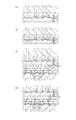
図10(a)〜(g)に示す工程は、図1で説明した工程Aに相当する。 The steps shown in FIGS. 10A to 10G correspond to the step A described in FIG.
図10(a)は、半導体層100を有する半導体ウエハとして、SOIウエハを用いていることを示している。SOIウエハは、半導体層100を支持する基体120と、半導体層100と基体120との間に配された絶縁体層110と、を含む。
FIG. 10A shows that an SOI wafer is used as a semiconductor wafer having the
図10(b)に示すように、各種半導体素子が形成された半導体層100の上に、層間絶縁層130を形成する。
As shown in FIG. 10B, an
図10(c)に示すように、層間絶縁層130を貫通して半導体素子に接続されたコンタクトプラグ131を形成する。
As shown in FIG. 10C, a
図10(d)は、半導体層100に孔281を形成する工程を示している。絶縁体膜160の上にレジストを塗布し、レジストの露光、現像を行なってマスクを形成する。マスクを用いて半導体層100をドライエッチングすることにより、半導体層100に孔281を形成する。本例において、孔281は半導体層100および絶縁体層110を貫通して基体120に達しているが、孔281を絶縁体層110内で止めてもよいし、半導体層100内で止めてもよい。なお、孔281が半導体層100に達するために、半導体層100のエッチングの前に、層間絶縁層130や素子分離部101のフィールド絶縁膜もエッチングする。図10(c)は、孔281の形成後に、レジストマスクを除去した状態を示している。なお、孔281とコンタクトプラグ131の形成はどちらが先でもよく、エッチングレートの違いを利用して同時に形成してもよい。
FIG. 10D shows a process of forming the hole 281 in the
図10(e)は孔281内に絶縁膜282を形成した状態を示している。 FIG. 10E shows a state where an insulating film 282 is formed in the hole 281.
図10(f)は孔281内にタングステン(W)を含む導電部材283を埋め込んだ工程を示している。 FIG. 10F shows a process in which a conductive member 283 containing tungsten (W) is embedded in the hole 281.
図10(g)は、層間絶縁層130の上に、導電部材283およびコンタクトプラグ131を覆う様に保護膜240を形成する工程を示している。
FIG. 10G shows a step of forming a protective film 240 on the
図11(h)に示す工程は、図1で説明した工程Bに相当する。受光基板10に支持基板20を貼り合わせ、相互に固定する。
The process shown in FIG. 11H corresponds to the process B described in FIG. The
図11(i)に示す工程は、図1で説明した工程Cに相当する。受光基板10を機械研磨(MP)、化学機械研磨(CMP)、あるいはウェットエッチングにより薄化する。本例では、受光基板10に対して支持基板20の側とは反対側に、孔281内の導電部材283を露出させる。受光基板10の薄化において除去されるべき部分は、孔281の深さに応じて設定される。孔281が絶縁体層110を貫通していれば、基体120を除去すれば導電部材283を露出できる。孔281が絶縁体層110を貫通していれば、基体120を除去すれば導電部材283を露出できる。孔281が絶縁体層110内にとどまっていれば、基体120および絶縁体層110の少なくとも一部を除去すれば導電部材283を露出できる。孔281が半導体層100を貫通していなければ、絶縁体層110を除去し、さらに半導体層100の一部を除去する必要がある。絶縁体層110を残しておく方が半導体層100に生じるダメージを低減できる。
The process shown in FIG. 11I corresponds to the process C described in FIG. The
図11(j)では受光基板001と回路基板30とを接合する工程を示している。回路基板30には各種トランジスタ、抵抗、容量、配線が形成されており、最上層の配線層352に含まれる接続電極355が露出した状態にある。受光基板001と回路基板30とを接合することで、受光基板10側の導電部材283と回路基板30の電極355が導通する。
FIG. 11J shows a process of bonding the light receiving substrate 001 and the
図11(k)に示す工程は、図1で説明した工程Eに相当する。支持基板20を受光基板10上から除去する。除去方法は剥離でも、BG、CMP、ウェットエッチング何れの方法でも構わない。
The process shown in FIG. 11K corresponds to the process E described in FIG. The
図11(l)に示す工程では、保護膜240を除去する。 In the step shown in FIG. 11L, the protective film 240 is removed.
図12(m)に示す工程では、層間絶縁層130の上に、第1配線層132、層間絶縁層140、ビアプラグ141、第2配線層142、層間絶縁層150、ビアプラグ151、絶縁体膜160を形成する。なお、図11(l)に示す工程で保護膜240を除去せずに、保護膜240を層間絶縁層として利用してもよい。
In the step shown in FIG. 12M, the
図12(n)に示す工程では、図1で説明した工程Fに相当する。受光基板10の上に、カラーフィルタ191、マイクロレンズ192を形成する。
The process shown in FIG. 12N corresponds to the process F described in FIG. A color filter 191 and a microlens 192 are formed on the
実施例3では、配線層を形成する前に、支持基板20の接合と受光基板10の薄化、および支持基板20の除去を行なっている。これにより、カラーフィルタ191やマイクロレンズ192だけでなく、配線層へのダメージを抑制する事が出来る。また、銅配線を用いた場合、配線層と絶縁層あるいは配線層と拡散防止層の界面で剥がれを抑制できる。
In Example 3, the
図13(a)に示す工程は、図1で説明した工程Aに相当する。配線層132、142はダマシン構造を有する、銅配線である。第1配線層132はシングルダマシン構造、第2配線層142はデュアルダマシン構造を有する。また、第1配線層132と層間絶縁層150の間には拡散防止層133が配されており、第2配線層142と層間絶縁層150の間には拡散防止層143が配されている。拡散防止層143の上には絶縁層161が配されている。
The process shown in FIG. 13A corresponds to the process A described in FIG. The wiring layers 132 and 142 are copper wirings having a damascene structure. The
図13(b)に示す工程は、図1で説明した工程Bに相当する。受光基板10の絶縁層161上に支持基板20が接合される。
The process shown in FIG. 13B corresponds to the process B described in FIG. The
図13(c)に示す工程は、図1で説明した工程Cに相当する。受光基板10の半導体層100が薄化される。
The process shown in FIG. 13C corresponds to the process C described in FIG. The
図13(d)に示す工程は、実施例1における貫通電極を形成する工程に相当する。半導体層100を貫通する導電部材283が形成される。
The step shown in FIG. 13D corresponds to the step of forming the through electrode in Example 1. A conductive member 283 that penetrates the
図13(e)に示す工程は、図1で説明した工程Dに相当する。受光基板10に回路基板30が接合される。
The step shown in FIG. 13E corresponds to the step D described in FIG. The
図14(f)に示す工程は、図1で説明した工程Eに相当する。支持基板20が受光基板10の上から除去される。
The process shown in FIG. 14F corresponds to the process E described in FIG. The
図14(g)、(h)に示す工程は、図1で説明した工程Fに相当する。 The steps shown in FIGS. 14G and 14H correspond to the step F described in FIG.
図14(g)に示す工程では、導光部170を形成する。まず、光電変換素子PD上に開口を有するマスクを用いて、層間絶縁層161、150、140、130および拡散防止層143、133をエッチングする。これによって、開口部175を形成する。開口部175を形成する際に、図13(a)に示す工程で層間絶縁層130の下に配された絶縁層129がエッチングストップ層として機能する。さらに、開口部175の中に窒化シリコンや樹脂などの透光材料を埋め込むことにより、導光部170が形成される。開口部175の外に位置する透光材料は必要に応じて除去される。
In the step shown in FIG. 14G, the light guide unit 170 is formed. First, the
図14(g)に示す工程では、導光部170を覆って層間絶縁層162が形成される。さらに層間絶縁層162、161にビアプラグ151を形成し、ビアプラグ151の上にパッド電極152を形成する。パッド電極152を覆うようにパッシベーション膜としての絶縁体膜160を形成する。絶縁体膜160をエッチバック法等を用いて集光部161を有するように加工することができる。集光部161は層内レンズとして機能する。集光部161を形成する上で好適な絶縁体膜160は窒化シリコン膜でありうる。絶縁体膜160の上に樹脂からなる平坦化膜163を形成する。平坦化膜163の上にカラーフィルタ191、マイクロレンズ192を形成する。導光部170や集光部161、平坦化膜163、カラーフィルタ191、マイクロレンズ192は図1で説明した光学部材40に相当する。また、ビアプラグ151やパッド電極152、層間絶縁層162は、支持基板20の除去後に形成された配線部材50である。
In the step shown in FIG. 14G, the interlayer insulating layer 162 is formed so as to cover the light guide unit 170. Further, via plugs 151 are formed in the interlayer insulating layers 162 and 161, and pad electrodes 152 are formed on the via plugs 151. An insulator film 160 as a passivation film is formed so as to cover the pad electrode 152. The insulator film 160 can be processed to have the light collecting portion 161 by using an etch back method or the like. The condensing part 161 functions as an in-layer lens. The insulator film 160 suitable for forming the condensing part 161 may be a silicon nitride film. A planarizing film 163 made of resin is formed on the insulator film 160. A color filter 191 and a microlens 192 are formed on the planarization film 163. The light guide unit 170, the light collecting unit 161, the planarization film 163, the color filter 191 and the microlens 192 correspond to the
本実施形態は、導光部170を設けているために、半導体層100の受光面上に複数の配線層があっても、迷光等を抑制でき、また、光利用効率を向上できる。
In the present embodiment, since the light guide unit 170 is provided, stray light or the like can be suppressed and the light utilization efficiency can be improved even if there are a plurality of wiring layers on the light receiving surface of the
さらに、導光部170を、支持基板20の除去後に形成しているため、薄化時のダメージや支持基板20の除去時に生じ得るダメージが導光部170に与える影響を低減できる。
Furthermore, since the light guide unit 170 is formed after the
なお、本実施例では、実施例1のようにして配線層を薄化間に形成したが、実施例2のように、支持基板20の除去後に、複数の配線層や層間絶縁層を形成することもできる。また、貫通電極の形成は実施例2と同様でもよいし、実施例3と同様でもよい。
In this embodiment, the wiring layers are formed during thinning as in the first embodiment. However, as in the second embodiment, after the
以上説明した実施形態に関しては、本明細書に明確な記載がなくとも、添付の図面や技術常識から把握できる事項も本開示の一部を構成する。また、本発明は、本開示の技術思想の範囲を逸脱しない限り、適宜な変更が可能である。 Regarding the embodiment described above, even if there is no clear description in the present specification, matters that can be grasped from the attached drawings and common technical knowledge also constitute a part of the present disclosure. The present invention can be modified as appropriate without departing from the scope of the technical idea of the present disclosure.
10 受光基板
PD 光電変換素子
20 支持基板
30 回路基板
TR2、TR3 半導体素子
DESCRIPTION OF
Claims (13)
前記第2基板に固定された前記第1基板を、前記第1基板に対して前記第2基板の側とは反対側から薄化する工程と、
前記薄化された第1基板を、半導体素子が設けられた第3基板が前記第1基板に対して前記第2基板の側とは反対側に位置するように、前記第3基板に固定する工程と、
前記第1基板を前記第3基板に固定する工程の後に、前記第2基板を除去する工程と、を備えることを特徴とする光電変換装置の製造方法。 Fixing a first substrate including a semiconductor layer provided with a photoelectric conversion element to a second substrate;
Thinning the first substrate fixed to the second substrate from the side opposite to the second substrate with respect to the first substrate;
The thinned first substrate is fixed to the third substrate such that a third substrate provided with a semiconductor element is located on the opposite side of the second substrate from the first substrate. Process,
And a step of removing the second substrate after the step of fixing the first substrate to the third substrate.
Priority Applications (3)
| Application Number | Priority Date | Filing Date | Title |
|---|---|---|---|
| JP2016094171A JP2017204510A (en) | 2016-05-09 | 2016-05-09 | Method of manufacturing photoelectric conversion device |
| US15/584,748 US10559464B2 (en) | 2016-05-09 | 2017-05-02 | Method for manufacturing photoelectric conversion device |
| CN201710327951.3A CN107359210B (en) | 2016-05-09 | 2017-05-04 | Method for manufacturing photoelectric conversion apparatus |
Applications Claiming Priority (1)
| Application Number | Priority Date | Filing Date | Title |
|---|---|---|---|
| JP2016094171A JP2017204510A (en) | 2016-05-09 | 2016-05-09 | Method of manufacturing photoelectric conversion device |
Publications (2)
| Publication Number | Publication Date |
|---|---|
| JP2017204510A true JP2017204510A (en) | 2017-11-16 |
| JP2017204510A5 JP2017204510A5 (en) | 2019-06-06 |
Family
ID=60243642
Family Applications (1)
| Application Number | Title | Priority Date | Filing Date |
|---|---|---|---|
| JP2016094171A Pending JP2017204510A (en) | 2016-05-09 | 2016-05-09 | Method of manufacturing photoelectric conversion device |
Country Status (3)
| Country | Link |
|---|---|
| US (1) | US10559464B2 (en) |
| JP (1) | JP2017204510A (en) |
| CN (1) | CN107359210B (en) |
Cited By (3)
| Publication number | Priority date | Publication date | Assignee | Title |
|---|---|---|---|---|
| JP2020109841A (en) * | 2018-12-28 | 2020-07-16 | 清華大学Tsinghua University | Backside treatment process for backside illuminated photoelectric device |
| JP2021512507A (en) * | 2018-06-22 | 2021-05-13 | 中芯集成電路(寧波)有限公司 | Photoelectric detector and its manufacturing method, image sensor |
| US11764245B2 (en) | 2018-06-22 | 2023-09-19 | Ningbo Semiconductor International Corporation | Fabrication method of photodetector and imaging sensor |
Families Citing this family (4)
| Publication number | Priority date | Publication date | Assignee | Title |
|---|---|---|---|---|
| US10566287B1 (en) * | 2018-02-02 | 2020-02-18 | Inphi Corporation | Light engine based on silicon photonics TSV interposer |
| KR102551483B1 (en) * | 2018-08-14 | 2023-07-04 | 삼성전자주식회사 | Image sensor and method for fabricating the same |
| US11165509B1 (en) | 2020-06-05 | 2021-11-02 | Marvell Asia Pte, Ltd. | Method for co-packaging light engine chiplets on switch substrate |
| CN115542478B (en) * | 2022-11-25 | 2023-04-07 | 之江实验室 | Three-dimensional packaging structure and packaging method based on photoelectric chip double-sided process |
Citations (12)
| Publication number | Priority date | Publication date | Assignee | Title |
|---|---|---|---|---|
| JPH1117107A (en) * | 1997-06-27 | 1999-01-22 | Sony Corp | Three-dimensional circuit element and manufacture thereof |
| JP2005142221A (en) * | 2003-11-04 | 2005-06-02 | Sony Corp | Solid state imaging element and its manufacturing method |
| JP2005259828A (en) * | 2004-03-10 | 2005-09-22 | Sony Corp | Solid state imaging device and its manufacturing method |
| WO2006019156A1 (en) * | 2004-08-20 | 2006-02-23 | Zycube Co., Ltd. | Method for manufacturing semiconductor device having three-dimensional multilayer structure |
| JP2009055007A (en) * | 2007-08-24 | 2009-03-12 | Honda Motor Co Ltd | Semiconductor device |
| US20110042807A1 (en) * | 2009-08-19 | 2011-02-24 | Chien-Hung Liu | Chip package and fabrication method thereof |
| JP2011204915A (en) * | 2010-03-25 | 2011-10-13 | Sony Corp | Semiconductor apparatus, method of manufacturing semiconductor apparatus, method of designing semiconductor apparatus, and electronic apparatus |
| US20130264688A1 (en) * | 2012-04-06 | 2013-10-10 | Omnivision Technologies, Inc. | Method and apparatus providing integrated circuit system with interconnected stacked device wafers |
| JP2013251391A (en) * | 2012-05-31 | 2013-12-12 | Canon Inc | Method of manufacturing semiconductor device |
| JP2015135938A (en) * | 2013-12-19 | 2015-07-27 | ソニー株式会社 | Semiconductor device, method of manufacturing semiconductor device, and electronic apparatus |
| US20150279816A1 (en) * | 2014-03-28 | 2015-10-01 | Taiwan Semiconductor Manufacturing Company, Ltd. | Bonding Structure for Stacked Semiconductor Devices |
| JP2016025255A (en) * | 2014-07-22 | 2016-02-08 | 株式会社東芝 | Semiconductor device and manufacturing method thereof |
Family Cites Families (13)
| Publication number | Priority date | Publication date | Assignee | Title |
|---|---|---|---|---|
| US7232605B2 (en) * | 2003-07-17 | 2007-06-19 | Board Of Trustees Of Michigan State University | Hybrid natural-fiber composites with cellular skeletal structures |
| JP4691939B2 (en) | 2004-09-27 | 2011-06-01 | ソニー株式会社 | Manufacturing method of back-illuminated solid-state imaging device |
| JP4816603B2 (en) | 2007-09-10 | 2011-11-16 | ソニー株式会社 | Manufacturing method of solid-state imaging device |
| JP4816602B2 (en) | 2007-09-10 | 2011-11-16 | ソニー株式会社 | Manufacturing method of solid-state imaging device |
| JP4858367B2 (en) | 2007-09-10 | 2012-01-18 | ソニー株式会社 | Manufacturing method of solid-state imaging device |
| JP5489705B2 (en) | 2009-12-26 | 2014-05-14 | キヤノン株式会社 | Solid-state imaging device and imaging system |
| US8395919B2 (en) * | 2010-07-29 | 2013-03-12 | General Electric Company | Photovoltaic inverter system and method of starting same at high open-circuit voltage |
| JP5218502B2 (en) | 2010-08-30 | 2013-06-26 | ソニー株式会社 | Method for manufacturing solid-state imaging device |
| CN103545275B (en) | 2012-07-12 | 2016-02-17 | 中芯国际集成电路制造(上海)有限公司 | Silicon through hole encapsulating structure and formation method |
| US8878325B2 (en) | 2012-07-31 | 2014-11-04 | Taiwan Semiconductor Manufacturing Company, Ltd. | Elevated photodiode with a stacked scheme |
| US9525001B2 (en) * | 2014-12-30 | 2016-12-20 | Taiwan Semiconductor Manufacturing Co., Ltd. | Semiconductor device and manufacturing method thereof |
| US10177187B2 (en) * | 2015-05-28 | 2019-01-08 | Taiwan Semiconductor Manufacturing Company Ltd. | Implant damage free image sensor and method of the same |
| US9620548B1 (en) * | 2015-10-30 | 2017-04-11 | Taiwan Semiconductor Manufacturing Co., Ltd. | Image sensor with wide contact |
-
2016
- 2016-05-09 JP JP2016094171A patent/JP2017204510A/en active Pending
-
2017
- 2017-05-02 US US15/584,748 patent/US10559464B2/en active Active
- 2017-05-04 CN CN201710327951.3A patent/CN107359210B/en active Active
Patent Citations (12)
| Publication number | Priority date | Publication date | Assignee | Title |
|---|---|---|---|---|
| JPH1117107A (en) * | 1997-06-27 | 1999-01-22 | Sony Corp | Three-dimensional circuit element and manufacture thereof |
| JP2005142221A (en) * | 2003-11-04 | 2005-06-02 | Sony Corp | Solid state imaging element and its manufacturing method |
| JP2005259828A (en) * | 2004-03-10 | 2005-09-22 | Sony Corp | Solid state imaging device and its manufacturing method |
| WO2006019156A1 (en) * | 2004-08-20 | 2006-02-23 | Zycube Co., Ltd. | Method for manufacturing semiconductor device having three-dimensional multilayer structure |
| JP2009055007A (en) * | 2007-08-24 | 2009-03-12 | Honda Motor Co Ltd | Semiconductor device |
| US20110042807A1 (en) * | 2009-08-19 | 2011-02-24 | Chien-Hung Liu | Chip package and fabrication method thereof |
| JP2011204915A (en) * | 2010-03-25 | 2011-10-13 | Sony Corp | Semiconductor apparatus, method of manufacturing semiconductor apparatus, method of designing semiconductor apparatus, and electronic apparatus |
| US20130264688A1 (en) * | 2012-04-06 | 2013-10-10 | Omnivision Technologies, Inc. | Method and apparatus providing integrated circuit system with interconnected stacked device wafers |
| JP2013251391A (en) * | 2012-05-31 | 2013-12-12 | Canon Inc | Method of manufacturing semiconductor device |
| JP2015135938A (en) * | 2013-12-19 | 2015-07-27 | ソニー株式会社 | Semiconductor device, method of manufacturing semiconductor device, and electronic apparatus |
| US20150279816A1 (en) * | 2014-03-28 | 2015-10-01 | Taiwan Semiconductor Manufacturing Company, Ltd. | Bonding Structure for Stacked Semiconductor Devices |
| JP2016025255A (en) * | 2014-07-22 | 2016-02-08 | 株式会社東芝 | Semiconductor device and manufacturing method thereof |
Cited By (4)
| Publication number | Priority date | Publication date | Assignee | Title |
|---|---|---|---|---|
| JP2021512507A (en) * | 2018-06-22 | 2021-05-13 | 中芯集成電路(寧波)有限公司 | Photoelectric detector and its manufacturing method, image sensor |
| JP7055902B2 (en) | 2018-06-22 | 2022-04-18 | 中芯集成電路(寧波)有限公司 | Photoelectric detector and its manufacturing method, image sensor |
| US11764245B2 (en) | 2018-06-22 | 2023-09-19 | Ningbo Semiconductor International Corporation | Fabrication method of photodetector and imaging sensor |
| JP2020109841A (en) * | 2018-12-28 | 2020-07-16 | 清華大学Tsinghua University | Backside treatment process for backside illuminated photoelectric device |
Also Published As
| Publication number | Publication date |
|---|---|
| CN107359210A (en) | 2017-11-17 |
| CN107359210B (en) | 2020-03-10 |
| US20170323787A1 (en) | 2017-11-09 |
| US10559464B2 (en) | 2020-02-11 |
Similar Documents
| Publication | Publication Date | Title |
|---|---|---|
| US11637141B2 (en) | Solid-state image pickup apparatus and image pickup system | |
| CN107359210B (en) | Method for manufacturing photoelectric conversion apparatus | |
| US9263488B2 (en) | Semiconductor device, manufacturing method of semiconductor device, semiconductor wafer, and electronic equipment | |
| JP5517800B2 (en) | Member for solid-state imaging device and method for manufacturing solid-state imaging device | |
| JP5843475B2 (en) | Solid-state imaging device and method for manufacturing solid-state imaging device | |
| KR101032182B1 (en) | Semiconductor package and camera module | |
| TWI566338B (en) | Imaging apparatus, imaging system and method of fabricating dual-facing camera assembly | |
| JP5553693B2 (en) | Solid-state imaging device and imaging system | |
| US20120008934A1 (en) | Camera module and method of manufacturing the same | |
| JP6140965B2 (en) | Semiconductor device and manufacturing method thereof | |
| KR20110060802A (en) | Solid-state imaging device, method of manufacturing the same, and electronic apparatus | |
| JP2020057812A (en) | Semiconductor device and electronic equipment | |
| KR20100028623A (en) | Imagers with contact plugs extending through the substrates thereof and imager fabrication methods | |
| JP2023055816A (en) | Solid state image pickup device and solid state image pickup device manufacturing method | |
| US11276723B2 (en) | Semiconductor device, apparatus, and method for producing semiconductor device | |
| US9312292B2 (en) | Back side illumination image sensor and manufacturing method thereof | |
| TW201803100A (en) | Semiconductor device and method for fabricating the same | |
| CN105185801B (en) | Solid-state image pickup device and image pickup system | |
| JP2009158957A (en) | Method of manufacturing image sensor | |
| JP6385515B2 (en) | Semiconductor device and manufacturing method thereof | |
| JP2023088114A (en) | Photoelectric conversion device, apparatus, and method for manufacturing photoelectric conversion device | |
| JP2020053701A (en) | Method for manufacturing semiconductor device |
Legal Events
| Date | Code | Title | Description |
|---|---|---|---|
| A521 | Request for written amendment filed |
Free format text: JAPANESE INTERMEDIATE CODE: A523 Effective date: 20190425 |
|
| A621 | Written request for application examination |
Free format text: JAPANESE INTERMEDIATE CODE: A621 Effective date: 20190425 |
|
| A977 | Report on retrieval |
Free format text: JAPANESE INTERMEDIATE CODE: A971007 Effective date: 20200205 |
|
| A131 | Notification of reasons for refusal |
Free format text: JAPANESE INTERMEDIATE CODE: A131 Effective date: 20200331 |
|
| A02 | Decision of refusal |
Free format text: JAPANESE INTERMEDIATE CODE: A02 Effective date: 20201110 |