KR101032182B1 - Semiconductor package and camera module - Google Patents
Semiconductor package and camera module Download PDFInfo
- Publication number
- KR101032182B1 KR101032182B1 KR1020097014440A KR20097014440A KR101032182B1 KR 101032182 B1 KR101032182 B1 KR 101032182B1 KR 1020097014440 A KR1020097014440 A KR 1020097014440A KR 20097014440 A KR20097014440 A KR 20097014440A KR 101032182 B1 KR101032182 B1 KR 101032182B1
- Authority
- KR
- South Korea
- Prior art keywords
- main surface
- semiconductor substrate
- cavity
- adhesive
- electrode
- Prior art date
Links
- 239000004065 semiconductor Substances 0.000 title claims abstract description 88
- 239000000758 substrate Substances 0.000 claims abstract description 162
- 238000003384 imaging method Methods 0.000 claims abstract description 56
- 239000000853 adhesive Substances 0.000 claims abstract description 44
- 230000001070 adhesive effect Effects 0.000 claims abstract description 44
- 238000000034 method Methods 0.000 claims description 38
- 239000011347 resin Substances 0.000 claims description 23
- 229920005989 resin Polymers 0.000 claims description 23
- 230000002787 reinforcement Effects 0.000 claims description 2
- 230000003014 reinforcing effect Effects 0.000 claims description 2
- 239000007787 solid Substances 0.000 abstract 3
- XUIMIQQOPSSXEZ-UHFFFAOYSA-N Silicon Chemical compound [Si] XUIMIQQOPSSXEZ-UHFFFAOYSA-N 0.000 description 85
- 229910052710 silicon Inorganic materials 0.000 description 85
- 239000010703 silicon Substances 0.000 description 85
- 230000008569 process Effects 0.000 description 24
- 239000010410 layer Substances 0.000 description 20
- 239000011521 glass Substances 0.000 description 19
- 238000004519 manufacturing process Methods 0.000 description 19
- 229910000679 solder Inorganic materials 0.000 description 14
- 230000015572 biosynthetic process Effects 0.000 description 12
- 238000001459 lithography Methods 0.000 description 10
- 238000005530 etching Methods 0.000 description 9
- 239000011229 interlayer Substances 0.000 description 8
- 239000002184 metal Substances 0.000 description 8
- 229910052751 metal Inorganic materials 0.000 description 8
- 239000004020 conductor Substances 0.000 description 7
- 238000010586 diagram Methods 0.000 description 7
- 230000002093 peripheral effect Effects 0.000 description 7
- 230000001681 protective effect Effects 0.000 description 6
- 238000001039 wet etching Methods 0.000 description 6
- 239000004925 Acrylic resin Substances 0.000 description 5
- 229920000178 Acrylic resin Polymers 0.000 description 5
- 239000000463 material Substances 0.000 description 5
- 238000004544 sputter deposition Methods 0.000 description 5
- 239000002585 base Substances 0.000 description 4
- 239000003795 chemical substances by application Substances 0.000 description 4
- 238000005229 chemical vapour deposition Methods 0.000 description 4
- 238000004140 cleaning Methods 0.000 description 4
- 230000000694 effects Effects 0.000 description 4
- 229910004298 SiO 2 Inorganic materials 0.000 description 3
- 238000012360 testing method Methods 0.000 description 3
- PPBRXRYQALVLMV-UHFFFAOYSA-N Styrene Chemical compound C=CC1=CC=CC=C1 PPBRXRYQALVLMV-UHFFFAOYSA-N 0.000 description 2
- 230000003321 amplification Effects 0.000 description 2
- 238000004380 ashing Methods 0.000 description 2
- 238000005452 bending Methods 0.000 description 2
- 230000000903 blocking effect Effects 0.000 description 2
- 239000000919 ceramic Substances 0.000 description 2
- 238000009713 electroplating Methods 0.000 description 2
- 238000002955 isolation Methods 0.000 description 2
- 238000012986 modification Methods 0.000 description 2
- 230000004048 modification Effects 0.000 description 2
- 238000003199 nucleic acid amplification method Methods 0.000 description 2
- 238000000059 patterning Methods 0.000 description 2
- 238000012545 processing Methods 0.000 description 2
- 238000005476 soldering Methods 0.000 description 2
- 238000004528 spin coating Methods 0.000 description 2
- KXGFMDJXCMQABM-UHFFFAOYSA-N 2-methoxy-6-methylphenol Chemical compound [CH]OC1=CC=CC([CH])=C1O KXGFMDJXCMQABM-UHFFFAOYSA-N 0.000 description 1
- 229910017944 Ag—Cu Inorganic materials 0.000 description 1
- 229910004541 SiN Inorganic materials 0.000 description 1
- 229910020816 Sn Pb Inorganic materials 0.000 description 1
- 229910020836 Sn-Ag Inorganic materials 0.000 description 1
- 229910020888 Sn-Cu Inorganic materials 0.000 description 1
- 229910020922 Sn-Pb Inorganic materials 0.000 description 1
- 229910020988 Sn—Ag Inorganic materials 0.000 description 1
- 229910019204 Sn—Cu Inorganic materials 0.000 description 1
- 229910008783 Sn—Pb Inorganic materials 0.000 description 1
- 239000003513 alkali Substances 0.000 description 1
- 150000001412 amines Chemical class 0.000 description 1
- 230000005540 biological transmission Effects 0.000 description 1
- 230000008859 change Effects 0.000 description 1
- 229910052802 copper Inorganic materials 0.000 description 1
- 238000005260 corrosion Methods 0.000 description 1
- 230000007797 corrosion Effects 0.000 description 1
- 238000005336 cracking Methods 0.000 description 1
- 239000000428 dust Substances 0.000 description 1
- 238000005516 engineering process Methods 0.000 description 1
- 230000005496 eutectics Effects 0.000 description 1
- 238000000227 grinding Methods 0.000 description 1
- 238000007689 inspection Methods 0.000 description 1
- 238000003475 lamination Methods 0.000 description 1
- 230000000873 masking effect Effects 0.000 description 1
- 230000008018 melting Effects 0.000 description 1
- 238000002844 melting Methods 0.000 description 1
- 238000004806 packaging method and process Methods 0.000 description 1
- 239000002245 particle Substances 0.000 description 1
- 230000000149 penetrating effect Effects 0.000 description 1
- 239000005011 phenolic resin Substances 0.000 description 1
- 229920001568 phenolic resin Polymers 0.000 description 1
- 238000007747 plating Methods 0.000 description 1
- 238000005498 polishing Methods 0.000 description 1
- 229920001690 polydopamine Polymers 0.000 description 1
- 229920001721 polyimide Polymers 0.000 description 1
- 239000009719 polyimide resin Substances 0.000 description 1
- 238000007790 scraping Methods 0.000 description 1
- 229910052814 silicon oxide Inorganic materials 0.000 description 1
- 239000000126 substance Substances 0.000 description 1
- 230000003746 surface roughness Effects 0.000 description 1
- 238000012546 transfer Methods 0.000 description 1
Images


Classifications
-
- H—ELECTRICITY
- H01—ELECTRIC ELEMENTS
- H01L—SEMICONDUCTOR DEVICES NOT COVERED BY CLASS H10
- H01L27/00—Devices consisting of a plurality of semiconductor or other solid-state components formed in or on a common substrate
- H01L27/14—Devices consisting of a plurality of semiconductor or other solid-state components formed in or on a common substrate including semiconductor components sensitive to infrared radiation, light, electromagnetic radiation of shorter wavelength or corpuscular radiation and specially adapted either for the conversion of the energy of such radiation into electrical energy or for the control of electrical energy by such radiation
-
- H—ELECTRICITY
- H01—ELECTRIC ELEMENTS
- H01L—SEMICONDUCTOR DEVICES NOT COVERED BY CLASS H10
- H01L23/00—Details of semiconductor or other solid state devices
- H01L23/48—Arrangements for conducting electric current to or from the solid state body in operation, e.g. leads, terminal arrangements ; Selection of materials therefor
- H01L23/481—Internal lead connections, e.g. via connections, feedthrough structures
-
- H—ELECTRICITY
- H04—ELECTRIC COMMUNICATION TECHNIQUE
- H04N—PICTORIAL COMMUNICATION, e.g. TELEVISION
- H04N23/00—Cameras or camera modules comprising electronic image sensors; Control thereof
- H04N23/57—Mechanical or electrical details of cameras or camera modules specially adapted for being embedded in other devices
-
- H—ELECTRICITY
- H01—ELECTRIC ELEMENTS
- H01L—SEMICONDUCTOR DEVICES NOT COVERED BY CLASS H10
- H01L27/00—Devices consisting of a plurality of semiconductor or other solid-state components formed in or on a common substrate
- H01L27/14—Devices consisting of a plurality of semiconductor or other solid-state components formed in or on a common substrate including semiconductor components sensitive to infrared radiation, light, electromagnetic radiation of shorter wavelength or corpuscular radiation and specially adapted either for the conversion of the energy of such radiation into electrical energy or for the control of electrical energy by such radiation
- H01L27/144—Devices controlled by radiation
- H01L27/146—Imager structures
- H01L27/14601—Structural or functional details thereof
- H01L27/14618—Containers
-
- H—ELECTRICITY
- H01—ELECTRIC ELEMENTS
- H01L—SEMICONDUCTOR DEVICES NOT COVERED BY CLASS H10
- H01L27/00—Devices consisting of a plurality of semiconductor or other solid-state components formed in or on a common substrate
- H01L27/14—Devices consisting of a plurality of semiconductor or other solid-state components formed in or on a common substrate including semiconductor components sensitive to infrared radiation, light, electromagnetic radiation of shorter wavelength or corpuscular radiation and specially adapted either for the conversion of the energy of such radiation into electrical energy or for the control of electrical energy by such radiation
- H01L27/144—Devices controlled by radiation
- H01L27/146—Imager structures
- H01L27/14601—Structural or functional details thereof
- H01L27/14625—Optical elements or arrangements associated with the device
-
- H—ELECTRICITY
- H01—ELECTRIC ELEMENTS
- H01L—SEMICONDUCTOR DEVICES NOT COVERED BY CLASS H10
- H01L2224/00—Indexing scheme for arrangements for connecting or disconnecting semiconductor or solid-state bodies and methods related thereto as covered by H01L24/00
- H01L2224/01—Means for bonding being attached to, or being formed on, the surface to be connected, e.g. chip-to-package, die-attach, "first-level" interconnects; Manufacturing methods related thereto
- H01L2224/02—Bonding areas; Manufacturing methods related thereto
- H01L2224/023—Redistribution layers [RDL] for bonding areas
- H01L2224/0237—Disposition of the redistribution layers
- H01L2224/02372—Disposition of the redistribution layers connecting to a via connection in the semiconductor or solid-state body
-
- H—ELECTRICITY
- H01—ELECTRIC ELEMENTS
- H01L—SEMICONDUCTOR DEVICES NOT COVERED BY CLASS H10
- H01L2224/00—Indexing scheme for arrangements for connecting or disconnecting semiconductor or solid-state bodies and methods related thereto as covered by H01L24/00
- H01L2224/01—Means for bonding being attached to, or being formed on, the surface to be connected, e.g. chip-to-package, die-attach, "first-level" interconnects; Manufacturing methods related thereto
- H01L2224/02—Bonding areas; Manufacturing methods related thereto
- H01L2224/03—Manufacturing methods
- H01L2224/039—Methods of manufacturing bonding areas involving a specific sequence of method steps
- H01L2224/0392—Methods of manufacturing bonding areas involving a specific sequence of method steps specifically adapted to include a probing step
-
- H—ELECTRICITY
- H01—ELECTRIC ELEMENTS
- H01L—SEMICONDUCTOR DEVICES NOT COVERED BY CLASS H10
- H01L2224/00—Indexing scheme for arrangements for connecting or disconnecting semiconductor or solid-state bodies and methods related thereto as covered by H01L24/00
- H01L2224/01—Means for bonding being attached to, or being formed on, the surface to be connected, e.g. chip-to-package, die-attach, "first-level" interconnects; Manufacturing methods related thereto
- H01L2224/02—Bonding areas; Manufacturing methods related thereto
- H01L2224/04—Structure, shape, material or disposition of the bonding areas prior to the connecting process
- H01L2224/0401—Bonding areas specifically adapted for bump connectors, e.g. under bump metallisation [UBM]
-
- H—ELECTRICITY
- H01—ELECTRIC ELEMENTS
- H01L—SEMICONDUCTOR DEVICES NOT COVERED BY CLASS H10
- H01L2224/00—Indexing scheme for arrangements for connecting or disconnecting semiconductor or solid-state bodies and methods related thereto as covered by H01L24/00
- H01L2224/01—Means for bonding being attached to, or being formed on, the surface to be connected, e.g. chip-to-package, die-attach, "first-level" interconnects; Manufacturing methods related thereto
- H01L2224/02—Bonding areas; Manufacturing methods related thereto
- H01L2224/04—Structure, shape, material or disposition of the bonding areas prior to the connecting process
- H01L2224/05—Structure, shape, material or disposition of the bonding areas prior to the connecting process of an individual bonding area
- H01L2224/0554—External layer
- H01L2224/05541—Structure
- H01L2224/05548—Bonding area integrally formed with a redistribution layer on the semiconductor or solid-state body
-
- H—ELECTRICITY
- H01—ELECTRIC ELEMENTS
- H01L—SEMICONDUCTOR DEVICES NOT COVERED BY CLASS H10
- H01L2224/00—Indexing scheme for arrangements for connecting or disconnecting semiconductor or solid-state bodies and methods related thereto as covered by H01L24/00
- H01L2224/01—Means for bonding being attached to, or being formed on, the surface to be connected, e.g. chip-to-package, die-attach, "first-level" interconnects; Manufacturing methods related thereto
- H01L2224/02—Bonding areas; Manufacturing methods related thereto
- H01L2224/04—Structure, shape, material or disposition of the bonding areas prior to the connecting process
- H01L2224/06—Structure, shape, material or disposition of the bonding areas prior to the connecting process of a plurality of bonding areas
- H01L2224/061—Disposition
- H01L2224/0618—Disposition being disposed on at least two different sides of the body, e.g. dual array
- H01L2224/06181—On opposite sides of the body
-
- H—ELECTRICITY
- H01—ELECTRIC ELEMENTS
- H01L—SEMICONDUCTOR DEVICES NOT COVERED BY CLASS H10
- H01L2224/00—Indexing scheme for arrangements for connecting or disconnecting semiconductor or solid-state bodies and methods related thereto as covered by H01L24/00
- H01L2224/01—Means for bonding being attached to, or being formed on, the surface to be connected, e.g. chip-to-package, die-attach, "first-level" interconnects; Manufacturing methods related thereto
- H01L2224/10—Bump connectors; Manufacturing methods related thereto
- H01L2224/12—Structure, shape, material or disposition of the bump connectors prior to the connecting process
- H01L2224/13—Structure, shape, material or disposition of the bump connectors prior to the connecting process of an individual bump connector
- H01L2224/13001—Core members of the bump connector
- H01L2224/1302—Disposition
- H01L2224/13022—Disposition the bump connector being at least partially embedded in the surface
-
- H—ELECTRICITY
- H01—ELECTRIC ELEMENTS
- H01L—SEMICONDUCTOR DEVICES NOT COVERED BY CLASS H10
- H01L2224/00—Indexing scheme for arrangements for connecting or disconnecting semiconductor or solid-state bodies and methods related thereto as covered by H01L24/00
- H01L2224/01—Means for bonding being attached to, or being formed on, the surface to be connected, e.g. chip-to-package, die-attach, "first-level" interconnects; Manufacturing methods related thereto
- H01L2224/10—Bump connectors; Manufacturing methods related thereto
- H01L2224/12—Structure, shape, material or disposition of the bump connectors prior to the connecting process
- H01L2224/13—Structure, shape, material or disposition of the bump connectors prior to the connecting process of an individual bump connector
- H01L2224/13001—Core members of the bump connector
- H01L2224/1302—Disposition
- H01L2224/13024—Disposition the bump connector being disposed on a redistribution layer on the semiconductor or solid-state body
-
- H—ELECTRICITY
- H01—ELECTRIC ELEMENTS
- H01L—SEMICONDUCTOR DEVICES NOT COVERED BY CLASS H10
- H01L2224/00—Indexing scheme for arrangements for connecting or disconnecting semiconductor or solid-state bodies and methods related thereto as covered by H01L24/00
- H01L2224/01—Means for bonding being attached to, or being formed on, the surface to be connected, e.g. chip-to-package, die-attach, "first-level" interconnects; Manufacturing methods related thereto
- H01L2224/10—Bump connectors; Manufacturing methods related thereto
- H01L2224/12—Structure, shape, material or disposition of the bump connectors prior to the connecting process
- H01L2224/13—Structure, shape, material or disposition of the bump connectors prior to the connecting process of an individual bump connector
- H01L2224/13001—Core members of the bump connector
- H01L2224/13099—Material
- H01L2224/131—Material with a principal constituent of the material being a metal or a metalloid, e.g. boron [B], silicon [Si], germanium [Ge], arsenic [As], antimony [Sb], tellurium [Te] and polonium [Po], and alloys thereof
-
- H—ELECTRICITY
- H01—ELECTRIC ELEMENTS
- H01L—SEMICONDUCTOR DEVICES NOT COVERED BY CLASS H10
- H01L2924/00—Indexing scheme for arrangements or methods for connecting or disconnecting semiconductor or solid-state bodies as covered by H01L24/00
- H01L2924/10—Details of semiconductor or other solid state devices to be connected
- H01L2924/11—Device type
- H01L2924/13—Discrete devices, e.g. 3 terminal devices
- H01L2924/1304—Transistor
- H01L2924/1306—Field-effect transistor [FET]
- H01L2924/13091—Metal-Oxide-Semiconductor Field-Effect Transistor [MOSFET]
Abstract
반도체 패키지는 고상 촬상 소자, 전극 패드, 스루홀 전극, 및 광투과 기판을 포함한다. 고상 촬상 소자는 반도체 기판의 제1 주면 상에 형성된다. 전극 패드는 반도체 기판의 제1 주면 상에 형성된다. 제1 주면 상에 형성된 전극 패드에 대향하는 제2 주면과 제1 주면 사이에 반도체 기판을 관통하여 연장하도록 스루홀 전극이 형성된다. 고상 촬상 소자 상에 공동을 형성하도록 패터닝된 접착제 상에 광투과 기판이 배치된다. 광투과 기판에서 보았을 때 공동의 아래에 있는 반도체 기판의 두께가 접착제의 아래에 있는 반도체 기판의 두께보다 크다.The semiconductor package includes a solid state imaging device, an electrode pad, a through hole electrode, and a light transmitting substrate. The solid-state imaging device is formed on the first main surface of the semiconductor substrate. The electrode pad is formed on the first main surface of the semiconductor substrate. A through hole electrode is formed to extend through the semiconductor substrate between the second main surface and the first main surface opposite to the electrode pad formed on the first main surface. A light transmissive substrate is disposed on the patterned adhesive to form a cavity on the solid state image pickup device. When viewed from a light transmissive substrate, the thickness of the semiconductor substrate under the cavity is greater than the thickness of the semiconductor substrate under the adhesive.
고상 촬상 소자, 스루홀 전극, 공동, 카메라 모듈 Solid State Imaging Devices, Through Hole Electrodes, Cavities, Camera Modules
Description
본 발명은 고상 촬상 소자(solid-state imaging element)를 이용한 반도체 패키지 및 그 반도체 패키지를 이용하는 카메라 모듈에 관련된다.The present invention relates to a semiconductor package using a solid-state imaging element and a camera module using the semiconductor package.
최근, 비디오 카메라들 및 디지털 카메라들이 널리 이용되고, CCD(charge coupled device)형 및 증폭형(amplification type) 고상 촬상 소자들이 이러한 카메라들에 이용된다. 특히, 휴대 전화들, PDA들 및 노트북 컴퓨터들과 같은 휴대용 전기 장치들이 널리 퍼지면서, 카메라 모듈의 크기, 무게, 두께 및 비용을 감소시키기 위한 요구가 증가하고 있다.Recently, video cameras and digital cameras are widely used, and charge coupled device (CCD) type and amplification type solid-state image pickup devices are used in such cameras. In particular, as portable electrical devices such as mobile phones, PDAs and notebook computers are widespread, there is an increasing demand for reducing the size, weight, thickness and cost of camera modules.
예를 들어, 종래의 소형 카메라 모듈의 촬상 소자로서 이용되는 증폭형 고상 촬상 소자(CMOS 이미지 센서)는 복수의 화소가 하나의 반도체 칩에 2차원적으로 배열된 촬상 화소부(imaging pixel portion), 및 촬상 화소부 외부에 형성된 주변 회로부(peripheral circuit portion)를 갖는다. 증폭형 고상 촬상 소자는 촬상 화소부의 각 화소에 예를 들면, 전송 및 증폭을 위한 다양한 MOS 트랜지스터를 갖는다. 포토다이오드들은 각 화소에 들어온 광을 광전기적으로(photoelectrically) 변환하여 신호 전하(signal charge)를 생성하고, 전송 트랜지스터 및 증폭 트랜지스터는 그 신호 전하를 전기 신호로 변환하고 증폭한다. 그 후 화소의 신호는 신호선을 통하여 주변 회로부에 출력된다.For example, an amplifying solid-state imaging device (CMOS image sensor) used as an imaging device of a conventional small camera module includes an imaging pixel portion in which a plurality of pixels are two-dimensionally arranged on one semiconductor chip; And a peripheral circuit portion formed outside the imaging pixel portion. The amplifying solid-state image pickup device has various MOS transistors, for example, for transmission and amplification in each pixel of the imaging pixel portion. Photodiodes photoelectrically convert light entering each pixel to generate signal charges, and transfer transistors and amplifying transistors convert and amplify the signal charges into electrical signals. The signal of the pixel is then output to the peripheral circuit portion through the signal line.
컬러 이미지를 얻기 위한 컬러 필터가 포토다이오드 상에 형성되고, 광을 효율적으로 집광시키기 위한 마이크로렌즈(microlens)가 컬러 필터 상에 형성된다. 상기 구성을 갖는 촬상 소자 칩은 (COB: 칩 온 보드에 의해) 수지 또는 세라믹으로 만들어진 인쇄 회로 기판 상에 직접 실장된다. 전극이 와이어 본딩에 의해 접속되고, 수동 소자가 (SMT: 표면 실장 기술에 의해) 표면에 실장된다. 커버 렌즈를 포함하는 렌즈 홀더가 인쇄 회로 기판 상에 배치되고 그에 부착됨으로써, 카메라 모듈을 형성한다.Color filters for obtaining color images are formed on the photodiodes, and microlens for collecting light efficiently are formed on the color filters. An imaging device chip having the above configuration is mounted directly on a printed circuit board made of resin or ceramic (by COB: chip on board). The electrodes are connected by wire bonding, and passive elements are mounted on the surface (by SMT: surface mount technology). A lens holder including a cover lens is disposed on and attached to the printed circuit board to form a camera module.
이러한 방법에서, 실장 영역은 촬상 소자의 영역보다 크고, 이것은 밀도를 무제한으로 증가시키는(크기, 무게 및 두께를 무제한으로 감소시키는) 것을 불가능하게 한다. 구성 부품들의 수가 많고 실장 공정이 복잡하기 때문에 비용을 감소시키는 것도 어렵다. 또한, 제조 공정에서 그라인더(grinder)를 이용하여 이면을 연삭(grinding)하여 반도체 기판을 얇게 하고, 수광면이 노출된 채로 다이싱에 의해 기판을 분할하는 것이 필요하다. 이것은 먼지 입자들이 수광면에 달라붙어 수율을 감소시킨다는 문제를 지닌다.In this way, the mounting area is larger than the area of the imaging device, which makes it impossible to increase the density indefinitely (unless reducing the size, weight and thickness). It is also difficult to reduce costs because of the large number of components and the complex mounting process. In addition, in the manufacturing process, it is necessary to grind the back surface by using a grinder to thin the semiconductor substrate, and to divide the substrate by dicing while the light receiving surface is exposed. This has the problem that dust particles stick to the light receiving surface and reduce the yield.
최근, 이러한 문제들을 해결하는 방법으로서, 광 투과 부재가 수광면 상에 부착되고 실리콘 기판의 수광면에 대향하는 면으로부터 전극이 추출되는(extracted) 패키지가 제안되어왔다(예를 들어, 일본 특허 출원 공개 공보 제2007-134735호).Recently, as a method of solving these problems, a package has been proposed in which a light transmitting member is attached on a light receiving surface and an electrode is extracted from a surface opposite to the light receiving surface of a silicon substrate (for example, Japanese patent application) Publication No. 2007-134735).
이러한 소형 카메라 모듈들에서, 포토다이오드 및 트랜지스터가 형성된 제1 주면 상의 전극으로부터 반도체 기판의 이면으로서의 제2 주면까지 반도체 기판을 관통하여 연장하는 전극을 추출할 때, 제조 처리량(throughput)을 증가시키기 위해 반도체 기판의 두께는 예를 들어, 약 100㎛로 감소되어야 한다.In such small camera modules, in order to increase the manufacturing throughput when extracting an electrode extending through the semiconductor substrate from the electrode on the first main surface on which the photodiode and transistor are formed to the second main surface as the back surface of the semiconductor substrate. The thickness of the semiconductor substrate should be reduced to about 100 μm, for example.
또한, 광을 효율적으로 포토다이오드에 집광시키기 위해서, 형성된 마이크로렌즈 재료의 굴절률보다 낮은 굴절률을 갖는 부재로 마이크로렌즈가 덮여야 한다. 그리하여, 마이크로렌즈 위의 공간이 최저 굴절률을 갖는 (대기압 또는 저기압) 기체로 채워지는 공동 구조(hollow structure)가 자주 이용된다. 투명한 부재가 공동(hollow)을 개재하여 마이크로렌즈 위에 배치된다. 이러한 투명한 부재는 패터닝된 접착제에 의해 마이크로렌즈로부터 이격된다.In addition, in order to focus light efficiently on the photodiode, the microlenses should be covered with a member having a refractive index lower than that of the formed microlens material. Thus, hollow structures are often used in which the space above the microlenses is filled with a gas having the lowest refractive index (atmospheric or low pressure). A transparent member is disposed over the microlens via a hollow. This transparent member is spaced apart from the microlens by the patterned adhesive.
불행하게도, 포토다이오드를 포함하는 촬상 소자 상에 공동이 형성되고 반도체 기판이 씨닝되면, 반도체 기판은 강도가 감소되어 공동이 형성된 영역에서 부서진다. 반도체 기판이 부서지지는 않더라도, 반도체 기판은 공동이 형성된 영역에서 구부러지고, 이것은 정상적인 이미지 표시를 불가능하게 한다.Unfortunately, when a cavity is formed on the imaging device including the photodiode and the semiconductor substrate is thinned, the semiconductor substrate is reduced in strength and breaks in the area where the cavity is formed. Although the semiconductor substrate is not broken, the semiconductor substrate is bent in the area where the cavity is formed, which makes normal image display impossible.
본 발명의 제1 측면에 따르면, 제1 반도체 패키지로서, 반도체 기판의 제1 주면 상에 형성된 고상 촬상 소자; 상기 반도체 기판의 상기 제1 주면 상에 형성된 전극 패드; 상기 제1 주면 상에 형성된 상기 전극 패드와 대향하는 제2 주면과 상기 제1 주면 사이에서 상기 반도체 기판을 관통하여 연장하도록 형성된 스루홀(through-hole) 전극; 및 상기 고상 촬상 소자 상에 공동을 형성하도록 패터닝된 접착제 상에 배치된 광투과 기판을 포함하는 제1 반도체 패키지가 제공된다. 광투과 기판으로부터 보았을 때 상기 공동의 아래에 있는 반도체 기판의 두께는 상기 접착제의 아래에 있는 반도체 기판의 두께보다 두껍다.According to a first aspect of the present invention, there is provided a first semiconductor package, comprising: a solid-state imaging device formed on a first main surface of a semiconductor substrate; An electrode pad formed on the first main surface of the semiconductor substrate; A through-hole electrode formed to extend through the semiconductor substrate between the second main surface and the first main surface facing the electrode pad formed on the first main surface; And a light transmitting substrate disposed on the adhesive patterned to form a cavity on the solid-state imaging device. When viewed from the light transmissive substrate, the thickness of the semiconductor substrate under the cavity is thicker than the thickness of the semiconductor substrate under the adhesive.
본 발명의 제2 측면에 따르면, 제2 반도체 패키지로서, 반도체 기판의 제1 주면 상에 형성된 고상 촬상 소자; 상기 반도체 기판의 상기 제1 주면 상에 형성된 전극 패드; 상기 제1 주면 상에 형성된 상기 전극 패드와 대향하는 제2 주면과 상기 제1 주면 사이에서 상기 반도체 기판을 관통하여 연장하도록 형성된 스루홀 전극; 및 상기 고상 촬상 소자 상에 공동을 형성하도록 패터닝된 접착제 상에 배치된 광투과 기판을 포함하는 제2 반도체 패키지가 제공된다. 광투과 기판으로부터 보았을 때 상기 접착제의 아래에 있는 반도체 기판의 제2 주면은 상기 공동의 아래에 있는 반도체 기판의 제2 주면보다 더욱 리세스된다.According to a second aspect of the present invention, there is provided a second semiconductor package, comprising: a solid-state imaging device formed on a first main surface of a semiconductor substrate; An electrode pad formed on the first main surface of the semiconductor substrate; A through-hole electrode formed to extend through the semiconductor substrate between the second main surface and the first main surface facing the electrode pad formed on the first main surface; And a light transmitting substrate disposed on the adhesive patterned to form a cavity on the solid-state imaging device. When viewed from the light transmissive substrate, the second main surface of the semiconductor substrate under the adhesive is recessed more than the second main surface of the semiconductor substrate under the cavity.
본 발명의 제3 측면에 따르면, 제1 및 제2 반도체 패키지 중 하나의 반도체 패키지; 상기 반도체 패키지의 광투과 기판 상에 형성된 적외선 차단 필터(infrared cut filter); 및 상기 적외선 차단 필터 상에 형성된 촬상 렌즈를 포함하는 카메라 모듈이 제공된다.According to a third aspect of the invention, a semiconductor package of one of the first and second semiconductor package; An infrared cut filter formed on the light transmitting substrate of the semiconductor package; And an imaging lens formed on the infrared cut filter.
도 1은 본 발명의 제1 실시예의 카메라 모듈의 구성을 도시하는 단면도이다.1 is a cross-sectional view showing the configuration of a camera module of a first embodiment of the present invention.
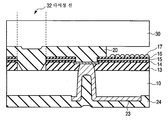
도 2는 제1 실시예의 카메라 모듈의 실리콘 반도체 기판 및 유리 기판의 부분들의 확대 단면도이다.2 is an enlarged cross-sectional view of portions of the silicon semiconductor substrate and the glass substrate of the camera module of the first embodiment.
도 3은 제1 실시예의 카메라 모듈 제조 방법을 도시하는 공정 흐름도이다.3 is a process flowchart showing the camera module manufacturing method of the first embodiment.
도 4는 본 발명의 제2 실시예의 카메라 모듈의 실리콘 반도체 기판 및 유리 기판의 부분들의 확대 단면도이다.4 is an enlarged cross-sectional view of portions of the silicon semiconductor substrate and the glass substrate of the camera module of the second embodiment of the present invention.
도 5는 제2 실시예의 카메라 모듈 제조 방법을 도시하는 공정 흐름도이다.Fig. 5 is a process flowchart showing the camera module manufacturing method of the second embodiment.
도 6은 본 발명의 제3 실시예의 카메라 모듈의 실리콘 반도체 기판 및 유리 기판의 부분들의 확대 단면도이다.6 is an enlarged cross-sectional view of portions of a silicon semiconductor substrate and a glass substrate of the camera module of the third embodiment of the present invention.
도 7은 제3 실시예의 카메라 모듈의 제조 방법을 도시하는 공정 흐름도이다.7 is a process flowchart showing the manufacturing method of the camera module of the third embodiment.
도 8은 제3 실시예의 카메라 모듈의 다른 제조 방법을 도시하는 공정 흐름도이다.8 is a process flowchart showing another manufacturing method of the camera module of the third embodiment.
도 9는 종래의 카메라 모듈의 다이싱 선 구조(dicing line structure)를 도시하는 단면도이다.9 is a cross-sectional view showing a dicing line structure of a conventional camera module.
도 10은 본 발명의 실시예의 카메라 모듈의 다이싱 선 구조를 도시하는 단면도이다.10 is a cross-sectional view showing a dicing line structure of the camera module of the embodiment of the present invention.
도 11은 다른 종래의 카메라 모듈의 다이싱 선 구조를 도시하는 단면도이다.11 is a cross-sectional view showing a dicing line structure of another conventional camera module.
도 12는 본 발명의 실시예의 다른 카메라 모듈의 다이싱 선 구조를 도시하는 단면도이다.12 is a cross-sectional view showing a dicing line structure of another camera module of the embodiment of the present invention.
첨부 도면을 참조하여 본 발명의 실시예들이 이하에서 설명될 것이다. 다음의 설명에서, 동일한 참조 번호는 도면 전체에 걸쳐 동일한 부분들을 표시한다.Embodiments of the present invention will be described below with reference to the accompanying drawings. In the following description, like reference numerals designate like parts throughout the drawings.
[제1 실시예][First Embodiment]
먼저, 본 발명의 제1 실시예의 카메라 모듈이 이하에서 설명될 것이다.First, the camera module of the first embodiment of the present invention will be described below.
도 1은 제1 실시예의 카메라 모듈의 구성을 도시하는 단면도이다. 촬상 소 자들(도시 안됨)은 실리콘 반도체 기판(촬상 소자 칩)(10)의 제1 주면 상에 형성된다. 예를 들어, 유리 기판(30)인 광투과 기판(투명 기판)은 촬상 소자들이 형성되지 않은, 실리콘 반도체 기판(10)의 제1 주면의 해당 영역 상의 접착제(20) 상에 형성된다. IR(InfraRed) 차단 필터(42)가 유리 기판(30) 상의 접착제(41) 상에 형성되고, 촬상 렌즈(40)를 포함하는 렌즈 홀더(50)가 접착제(43)를 개재하여 IR 차단 필터(42)를 덮는다. 이러한 구성요소들을 접착하여 카메라 모듈이 형성된다. 또한, 예를 들어 솔더 볼들(60)인 외부 단자들이 실리콘 반도체 기판(10)의 제2 주면 상에 형성된다. 차광(light-shielding) 전자기 실드(400)가 반도체 기판(10) 및 유리 기판(30) 주위에 형성되고, 접착제(45)에 의해 렌즈 홀더(50)에 접착된다. 그 후에, 예를 들면, 실리콘 반도체 기판(10)이 수지 또는 세라믹으로 만들어진 인쇄 회로 기판(70) 상에 솔더 볼들(60)을 개재하여 (칩 온 보드:COB에 의해) 직접 장착된다.1 is a cross-sectional view showing the configuration of the camera module of the first embodiment. Imaging elements (not shown) are formed on the first main surface of the silicon semiconductor substrate (imaging element chip) 10. For example, the light transmissive substrate (transparent substrate), which is the
도 1에 도시된 실리콘 반도체 기판(10) 및 유리 기판(30)의 단면 구조가 이하에서 자세하게 설명될 것이다.The cross-sectional structures of the
도 2는 카메라 모듈의 반도체 기판(10) 및 유리 기판(30)의 부분들의 확대 단면도이다. 카메라 모듈은 복수의 촬상 소자(12)가 2차원적으로 배열되는 촬상 화소부, 및 이러한 촬상 화소부를 제외한 영역에 형성되고 촬상 화소부로부터 출력된 신호들을 처리하는 주변 회로부를 갖는다.2 is an enlarged cross-sectional view of portions of the
카메라 모듈의 촬상 화소부는 이하의 구성을 갖는다. 도 2에서 도시된 바와 같이, 소자 분리 절연층으로서의 얕은 트렌치 분리(shallow trench isolation, STI)들(11) 및 STI들(11)에 의해 분리된 소자 영역들이 실리콘 반도체 기판(10)의 제1 주면 상에 배열된다. 포토다이오드 및 트랜지스터를 포함하는 촬상 소자(12)가 각 소자 영역에 형성된다. 층간 유전체막(13)이 촬상 소자들(12)이 형성된 제1 주면 상에 형성된다.The imaging pixel portion of the camera module has the following configuration. As shown in FIG. 2, device regions separated by shallow trench isolations (STIs) 11 and
기초층(base layer)(14)이 층간 유전체막(13) 상에 형성된다. 컬러 필터들(15)은 촬상 소자들(12)에 대향하도록 기초층(14) 상에 배열된다. 보호막(overcoat)(16)이 컬러 필터들(15) 상에 형성되고, 마이크로렌즈들(17)이 촬상 소자들(12)(컬러 필터들(15))에 대향하도록 보호막(16) 상에 형성된다. 공동(18)이 마이크로렌즈들(17) 상에 형성되고, 유리 기판(30)이 공동(18) 상에 배치된다.A
전술된 개별적인 부품들은 예를 들면, 이하의 재료들로 만들어진다. STI들(11)은 SiO2로 만들어지고, 층간 유전체막(13)은 Si02 또는 SiN으로 만들어진다. 컬러 필터들(15)은 아크릴 수지로 만들어지고, 마이크로렌즈들(17)은 스티렌계 수지(styrene-based resin)로 만들어진다.The individual parts described above are made of the following materials, for example. The
카메라 모듈의 주변 회로부에, 스루홀 전극과 전극 패드들이 형성되고, 이들은 이하에서 설명될 것이다. 실리콘 반도체 기판(10)에 제1 주면에 대향하는 제2 주면에서 제1 주면까지 스루홀이 형성된다. 절연막(22)이 스루홀의 내주면 및 제2 주면 상에 형성된다. 도체층(23)이 절연막(22) 상에 형성된다. 예를 들면, 솔더 레지스트(24)인 보호막이 도체층(23) 상에 형성된다. 도체층(23) 상의 솔더 레지스트(24)는 부분적으로 개방되어 있고, 솔더볼(60)이 노출된 도체층(23) 상에 형성 된다. 솔더볼(60)이 촬상 화소부의 아래에 있는 실리콘 반도체 기판(10)의 제2 주면 상에도 형성됨에 주목한다.Through-hole electrodes and electrode pads are formed in the peripheral circuit portion of the camera module, which will be described below. Through-holes are formed in the
솔더 레지스트(24)는 예를 들면, 페놀계 수지, 폴리이미드계 수지, 또는 아민계 수지로 만들어진다. 솔더볼(60)은 예를 들면, Sn-Pb(공융의(eutectic)), 95Pb-Sn(고연, 고융점 솔더), 또는 Sn-Ag, Sn-Cu, 또는 Sn-Ag-Cu와 같은 무연 솔더로 만들어진다.The soldering resist 24 is made of phenolic resin, polyimide resin, or amine resin, for example.
또한, 층간 유전체막(13)이 실리콘 반도체 기판의 제1 주면 상에 형성된다. 스루홀에 형성된 도체층(23)은 제1 주면에 이르고, 내부 전극(제1 전극 패드)(26)이 도체층(23) 상에 형성된다. 내부 전극(26)은 촬상 소자(12) 또는 주변 회로부에 형성된 주변 회로(도시 안됨)에 전기적으로 접속된다. 따라서, 스루홀에 형성된 스루홀 전극은 솔더볼(60) 및 촬상 소자(12) 또는 주변 회로에 전기적으로 접속한다.In addition, an
소자 표면 전극(제2 전극 패드)(27)이 층간 유전체막(13)을 개재하여 내부 전극(26) 상에 형성된다. 내부 전극(26)과 소자 표면 전극(27) 사이의 층간 유전체막(13)에, 이들 전극들을 전기적으로 접속하기 위한 접촉 플러그(도시 안됨)가 형성된다. 접촉 플러그 및 내부 전극(26)을 통하여 전압을 인가하거나 또는 신호를 판독하는 데 소자 표면 전극(27)이 이용된다. 특히 다이 분류 테스트를 실시할 때, 바늘이 소자 표면 전극(27)에 접촉한다.An element surface electrode (second electrode pad) 27 is formed on the
기초층(14)이 소자 표면 전극(27) 상에 형성된다. 아크릴 수지(19)가 기초층(14) 상에 형성되고, 보호막(16)이 아크릴 수지(19) 상에 형성된다. 패드 개 구(pad opening)가 소자 표면 전극(27) 상에 형성된 기초층(14), 아크릴 수지(19) 및 보호막(16)을 관통하여 형성된다.The
유리 기판(30)이 보호막(16)과 소자 표면 전극(27) 상의 접착제(20) 상에 형성된다. 접착제(20)는 패터닝되고 촬상 소자들(12)(마이크로렌즈들(17)) 상에 형성되지 않는데, 즉, 촬상 화소부 상에 형성되지 않는다. 전술된 바와 같이, 공동(18)이 촬상 화소부 상에 형성되고, 유리 기판(30)이 공동(18) 상에 배치된다.The
유리 기판(30)으로부터 보았을 때 공동(18)의 아래에 있는 실리콘 반도체 기판(10)의 두께는 접착제(20)의 아래에 있는 실리콘 반도체 기판(10)의 두께보다 크게 만들어진다. 예를 들면, t1를 접착제(20)의 아래에 있는 실리콘 기판(10)의 두께라고 하고 t2를 공동(18)의 아래에 있는 실리콘 기판(10)의 두께라고 하면, t1<t2 이다. 두께 t2는 바람직하게는 두께 t1보다 1.5㎛ 이상만큼 크다. 환언하면, 유리 기판(30)에서 보았을 때 접착제(20)의 아래에 있는 실리콘 기판(10)의 제2 주면은 공동(18)의 아래에 있는 실리콘 기판(10)의 제2 주면보다 더 리세스된다.When viewed from the
전술된 구조를 갖는 제1 실시예에서, 실리콘 기판(10)의 두께는, 유리 기판(30)에서 보았을 때 적어도 접착제(20)의 아래에 있는 스루홀(스루홀 전극)의 주변에서 작다. 이것은 스루홀의 처리를 용이하게 하고, 카메라 모듈의 제조의 효율성을 증가시킨다. 또한, 스루홀의 주변을 제외한 영역의 실리콘 기판(10)은 스루홀 주변의 영역의 실리콘 기판(10)보다 두껍기 때문에, 실리콘 기판(10)의 강도는 높다. 이것은 공동(18)이 형성된 영역의 실리콘 기판(10)이 파괴되거나, 공동(18)이 형성된 영역의 실리콘 기판(10)이 구부러져서 정상적인 이미지 표시가 불가능해 지는 문제를 방지할 수 있다.In the first embodiment having the above-described structure, the thickness of the
환언하면, 유리 기판(30)에서 보았을 때 공동(18)이 형성된 영역의 아래에 있는 실리콘 기판(10)의 두께, 즉 촬상 화소부 아래가 유리 기판(30)이 접착제(20)에 의해 접착된 비공동 영역(non-hollow region)의 아래에 있는 실리콘 기판(10)의 두께보다 크게 만들어진다. 이것은 공동(18)이 형성된 실리콘 기판(10)의 손쉬운 크래킹 및 구부러짐을 방지하고, 매우 믿을 수 있는 카메라 모듈이 형성될 수 있게 한다.In other words, when viewed from the
본 실시예에서, 패드 개구가 소자 표면 전극(27) 상의 기초층(14), 아크릴 수지(19), 및 보호막(16)을 통하여 형성된다. 그러나 이러한 막들을 관통하는 패드 개구가 형성되지 않는 구조를 이용하는 것도 가능하다. In this embodiment, a pad opening is formed through the
본 발명의 제1 실시예의 카메라 모듈 제조 방법이 이하에서 설명될 것이다. 도 3은 제1 실시예의 카메라 모듈 제조 방법을 도시하는 공정 흐름도이다.The camera module manufacturing method of the first embodiment of the present invention will be described below. 3 is a process flowchart showing the camera module manufacturing method of the first embodiment.
먼저, 고체 촬상 디바이스들이 실리콘 반도체 기판(웨이퍼)(10) 상에 형성된다(단계 S1). 즉, 각각이 포토다이오드 및 트랜지스터를 포함하는 촬상 소자들(12)이 실리콘 기판(10) 상에 형성된다. 또한, 내부 전극(26), 층간 유전체막(13), 소자 표면 전극(27), 컬러 필터들(15), 및 마이크로렌즈들(17)이 실리콘 기판(10) 상에 형성된다. 이어서, 다이 분류 테스트가 촬상 소자들(12)을 포함하는 각 칩 상에서 실시되고, 그리하여 칩이 정상적으로 동작하는지의 여부를 검사한다(단계 S2). 다이 분류 테스트에서, 테스터의 바늘이 소자 표면 전극(27)에 닿는다.First, solid-state imaging devices are formed on the silicon semiconductor substrate (wafer) 10 (step S1). That is,
그 후, 스핀 코팅 또는 적층에 의하여 실리콘 기판(10)의 제1 주면(소자 형성면) 상에 접착제(20)가 형성된다. 접착제(20)는 접착하는 기능 외에도 리소그래피에 의한 패터닝을 가능하게 하는 기능 및 패터닝된 형성을 유지하는 기능을 갖는다. 실리콘 기판(10) 위에 형성된 접착제(20)는 촬상 소자들(12)이 노출되도록, 즉 촬상 소자들(12) 상에 접착제가 형성되지 않도록 리소그래피에 의해 패터닝된다(단계 S3). 그 후, 접착제(20)를 갖는 실리콘 기판(10)이 유리 기판(30)에 부착된다(단계 S4).Thereafter, the adhesive 20 is formed on the first main surface (element formation surface) of the
그 후 실리콘 기판(10)은 백 그라인딩 등에 의해 제2 주면을 스크래핑(scraping)함으로써 씨닝된다(단계 S5). 선(streak)들이 실리콘 이면 상에 남고, 표면 거칠기는 수 ㎛ 내지 10㎛에 이른다. 후속 단계들에서 리소그래피 및 RIE로 공정이 바로 진행하면, 리소그래피 오차 또는 RIE 오차가 발생할 수 있다. 그리하여 바람직하게는, 예를 들어, 화학 기계적 연마(chemical mechanical polish, CMP) 또는 습식 에칭에 의해 제2 주면이 평탄화된다.Thereafter, the
또한, 실리콘 기판(10)의 두께의 변화는 평균값 ±5㎛의 범위 내에 속해야 한다. 실리콘 기판의 두께가 평면에서 변화한다면, 다음의 RIE 단계에서 실리콘이 두꺼운 부분에서는 불충분한 에칭이 발생하고 실리콘이 얇은 부분의 바닥 상에 노칭(notching)이라고 불리는 움푹 팬 곳(scoop)이 형성된다.In addition, the change in the thickness of the
그 후, 감광 수지가 도포되고, 공동(18)의 바로 아래에 있는 실리콘 기판(10)의 제2 주면 상에만 수지 마스크 패턴을 남기도록 패터닝된다(단계 S6). 이어서, 수지 마스크 패턴으로 보호되지 않은 실리콘 기판(10)의 제2 주면이 에칭된 다. 즉, 접착제(20)의 바로 아래에 있는 실리콘 기판(10)의 제2 주면이 에칭된다(단계 S7). 이러한 에칭에 의해, 접착제(20)의 바로 아래에 있는 실리콘 기판(10)의 제2 주면이 에칭되어 접착제(20)의 바로 아래에 있는 실리콘 기판(10)의 두께가, 공동(18)의 바로 아래에 있는 실리콘 기판(10)의 두께보다 얇게 된다. 에칭된 영역은 후속 단계에서 스루홀(through hole)이 형성되는 영역을 포함한다. 그 후, 레지스트 마스크 패턴이 제거된다(단계 S8).Thereafter, a photosensitive resin is applied and patterned so as to leave a resin mask pattern only on the second main surface of the
그 후, 실리콘 기판(10)의 제2 주면이 레지스트로 코팅되고, 실리콘 기판(10)의 제1 주면의 패드 개구에 대향하는 위치에, 리소그래피에 의해 구멍(hole)이 형성된다(단계 S9). 이 단계에서, 제2 주면의 개구를 제1 주면 상의 정렬 마크(도시 안됨)와 정렬하기 위해 더블 사이드 정렬기(double-side aligner) 또는 더블 사이드 스테퍼(double-side stepper)와 같은 수단이 이용될 수 있다. 이어서, 패터닝된 레지스트를 마스크로서 이용하여 스루홀이 형성된다(단계 S10).Thereafter, a second main surface of the
먼저, 실리콘 기판(10)의 실리콘만이 RIE에 의해 에칭된다. 촬상 소자들(12) 및 트랜지스터들을 형성하는 실리콘 디바이스 공정은 보통 웰 형성, STI 형성, 소스/드레인 형성, 게이트/전극 형성, 및 배선(interconnection) 형성의 순서로 진행된다. STI 형성에서, CMP 규칙들은 소정 크기를 초과하는 실리콘 힐(hill)도 소정 크기를 초과하는 얕은 트렌치도 형성을 금지한다. 크기가 큰 실리콘 힐이 CMP 동안 존재한다면, CMP 잔류물이 힐 상에 생성될 수 있다. 크기가 큰 얕은 트렌치가 존재하면, 트렌치에서 오버폴리싱(over-polishing)이 발생할 수 있다. 어느 경우에나, 다음 리소그래피 단계에서 부정합(misalignment)이 발생하거나, 또는 상부층의 금속 배선들의 절단(disconnection)이 발생할 수 있다. 그리하여, 통상적으로 더미(dummy) STI가 전극 패드와 같은 대형 패턴이 형성될 실리콘 기판의 부분에 형성되어, CMP 규칙들의 위배를 방지한다.First, only silicon of the
그러나 스루홀 전극을 형성할 때, CMP 규칙들에 반할지라도 전극 패드 아래에 STI를 형성하지 않는 것이 중요하다. 이것은 실리콘의 RIE 기체의 유형이 절연막의 RIE 기체의 유형과 다르기 때문이다. ', 실리콘의 RIE 동안 실리콘에 절연막 패턴이 존재하면, 이러한 부분에 에칭 오차가 발생하여 개구리 같은(frog-like) 에칭 잔류물이 형성될 수 있다. STI의 CMP 동안 CMP 잔류물이 불가피하게 전극 패드 아래에 생성된다면, 잔류물이 생성되는 부분에 리소그래피에 의해 구멍을 형성하고, 습식 에칭 등에 의해 재료가 부분적으로 에칭된 후에 CMP를 행하여 CMP 잔류물을 제거하는 것이 필요하다.However, when forming a through hole electrode, it is important not to form an STI under the electrode pad, even though it is against CMP rules. This is because the type of RIE gas of silicon is different from the type of RIE gas of the insulating film. If an insulating film pattern is present in the silicon during the RIE of the silicon, an etching error may occur in such a portion to form a frog-like etching residue. If CMP residues are inevitably produced under the electrode pads during CMP of the STI, holes are formed by lithography in the areas where the residues are produced, and CMP residues are subjected to CMP after the material is partially etched by wet etching or the like. It is necessary to remove.
또한, RIE에 의해 실리콘 기판에 형성된 스루홀의 형상은 바람직하게는 제2 주면의 개구로부터 안쪽을 향하여 차츰 좁아지는 테이퍼 형상(tapered shape)이다. 역 테이퍼가 노칭 또는 구부러짐(bowing)에 의해 형성되면, 절연막의 형성에서 CVD(chemical vapor deposition)에 의하여 또는 금속 시드층(metal seed layer)의 형성에서 스퍼터링에 의하여 오차가 발생할 수 있다.Further, the shape of the through hole formed in the silicon substrate by the RIE is preferably a tapered shape that gradually narrows inward from the opening of the second main surface. If the reverse taper is formed by notching or bowing, errors may occur by chemical vapor deposition (CVD) in the formation of the insulating film or by sputtering in the formation of the metal seed layer.
실리콘 기판(10)과 직접 접촉하는 층간 유전체막(13)의 층, 또는 실리콘 기판 상에 형성된 게이트 절연막이 실리콘의 RIE에서 스토퍼로서의 역할을 한다. 이어서, 애싱(ashing) 및 습식 클리닝(wet cleaning)에 의해 레지스트가 제거된다(단계 S11). 양호하게는 실리콘 RIE 또는 레지스트 제거 후에 HF계(HF-based) 습식 클리닝을 행함으로써 RIE 잔류물이 제거되는 것에 주목한다.A layer of the
그 후, SiO2, SiON, 또는 SiN으로 만들어진 절연막(22)이 CVD 등에 의하여 전체 제2 주면 상에 형성된다(단계 S12).Thereafter, an insulating film 22 made of SiO 2 , SiON, or SiN is formed on the entire second main surface by CVD or the like (step S12).
다시 레지스트가 도포되고, 실리콘 기판의 스루홀의 바닥에만 구멍이 형성되며(단계 S13), 절연막(22)의 RIE가 레지스트를 마스크로서 이용함으로써 행해진다(단계 S14). 절연막(22)의 RIE에서, 실리콘 디바이스 공정에 의해 미리 형성된 CVD 절연막 및 실리콘 기판(10)과 내부 전극(26) 사이에 형성된 모든 절연막이 에칭된다. 이러한 단계에서, 내부 전극(26)은 절연막들의 RIE 동안 스토퍼로서 기능한다.The resist is applied again, and a hole is formed only in the bottom of the through hole of the silicon substrate (step S13), and the RIE of the insulating film 22 is performed by using the resist as a mask (step S14). In the RIE of the insulating film 22, the CVD insulating film formed in advance by the silicon device process and all the insulating films formed between the
이어서, 애싱 및 습식 클리닝에 의하여 레지스트가 제거된다(단계 S15). 내부 전극(26)의 표면이 약 수 nm 내지 수십 nm만큼 산화될 수 있기 때문에, 바람직하게는 내부 전극(26)의 표면이 알칼리계(alkali-based) 습식 에칭에 의하여 약간 에칭된다는 것에 주목한다.Then, the resist is removed by ashing and wet cleaning (step S15). Note that since the surface of the
스퍼터링에 의해 금속 시드층이 절연막(22) 및 내부 전극(26)상에 형성된다(단계 S16). 이 스퍼터링 공정에서, 내부 전극(26)의 표면 상의 산화물 층이 바람직하게는 역 스퍼터링(reverse sputtering)에 의해 먼저 제거된다. 이어서, Ti 또는 Cu 와 같은 금속 시드가 스퍼터링된다. 내부 전극(26)의 표면 상의 부식을 방지하기 위해, 절연막(22)의 RIE와 금속 시드 스퍼터링 사이의 시간은 바람직하게는 3시간 이하이고, 최장 24시간 이하라는 것에 주목한다.By sputtering, a metal seed layer is formed on the insulating film 22 and the internal electrode 26 (step S16). In this sputtering process, the oxide layer on the surface of the
그 후, 전극 패터닝을 위해 레지스트가 제2 주면 상에 도포되고, 전극이 형성되지 않을 부분에만 남겨지도록 리소그래피에 의해 패터닝된다(단계 S17). 금속 시드층은 전기 도금(electroplating) 등에 의해 도금되고, 스루홀 전극 및 배선들이 형성된다(단계 S18). 그 후, 레지스트가 습식 에칭 등에 의해 제거된다(단계 S19). 이어서, 금속 시드가 예를 들어, 습식 클리닝에 의해 에칭되어 스루홀 전극 및 배선들을 제외한 영역의 절연막(22)을 노출시킨다(단계 S20). 먼저 논마스킹(non-masking) 전기 도금을 행하고, 그 후 리소그래피 및 에칭에 의하여 스루홀 전극 및 배선들을 형성하는 것도 가능하다는 것에 주목한다. 그러나 만약 이러한 방법이 이용된다면, 이용될 도금 용액의 양이 증가하여, 공정 비용을 고가로 만들 것이다.Thereafter, a resist is applied on the second main surface for electrode patterning, and patterned by lithography so as to remain only in the portion where the electrode will not be formed (step S17). The metal seed layer is plated by electroplating or the like, and through hole electrodes and wirings are formed (step S18). Thereafter, the resist is removed by wet etching or the like (step S19). Subsequently, the metal seed is etched by wet cleaning, for example, to expose the insulating film 22 in the region excluding the through hole electrode and the wirings (step S20). Note that it is also possible to first perform non-masking electroplating, and then form through hole electrodes and wirings by lithography and etching. However, if this method is used, the amount of plating solution to be used will increase, making the process cost expensive.
그 후, 솔더 레지스트(24)가 예를 들어, 스핀 코팅에 의해 제2 주면 전체 상에 형성된다. 솔더 볼(60)이 설치될 영역에만 리소그래피에 의해 솔더 레지스트(24)에 구멍이 형성된다(단계 S21). 그 후에, 도전 검사(conduction check)가 행해지고(단계 S22), 솔더볼(60)이 솔더 레지스트(24)의 구멍의 도체층(23) 상에 설치된다(단계 S23).Thereafter, the solder resist 24 is formed on the entire second main surface by, for example, spin coating. Holes are formed in the solder resist 24 by lithography only in the region where the
마지막으로, 실리콘 기판(10)이 다이싱에 의해 분할되고(단계 S24), 픽업(pickup)(단계 S25), 렌즈 탑재(단계 S26), 및 이미지 검사(렌즈 조정)(단계 S27)가 행해진다. 그 후에, 그것을 포장함으로써 카메라 모듈의 제조가 완료된다(단계 S28).Finally, the
[제2 실시예]Second Embodiment
다음으로, 본 발명의 제2 실시예의 카메라 모듈이 설명될 것이다. 전술된 제1 실시예의 구성에서와 동일한 참조 번호들은 동일한 부분들을 표시하고, 반복되는 설명은 생략될 것이다. Next, the camera module of the second embodiment of the present invention will be described. The same reference numerals as in the configuration of the above-described first embodiment denote the same parts, and the repeated description will be omitted.
도 4는 제2 실시예의 카메라 모듈의 실리콘 반도체 기판 및 유리 기판의 부분들의 확대 단면도이다.4 is an enlarged cross-sectional view of portions of the silicon semiconductor substrate and the glass substrate of the camera module of the second embodiment.
공동(18)의 아래에 있는 실리콘 기판(10)의 제2 주면 상에 실리콘 기판(10)의 표면에 수직인 방향으로 보강용 수지 마스크 패턴(31)이 형성된다. 이것은 공동(18)의 아래에 있는 실리콘 기판의 강도를 제1 실시예에 비하여 더 증가시키고, 공동(18)의 아래에 있는 실리콘 기판(10)이 파괴되거나, 이 영역의 실리콘 기판이 구부러져 정상적인 이미지 표시를 불가능하게 하는 문제를 방지할 수 있다. 나머지 구성 및 효과들은 제1 실시예의 구성 및 효과들과 동일하다.A reinforcing
수지 마스크 패턴(31)은 제1 실시예의 제조 방법에 있어서 공동(18)의 아래에 있는 부분을 제외한 영역(접착제(20) 아래)의 실리콘 기판(10)의 제2 주면을 에칭하는 데 이용된 마스크이며, 이러한 마스크를 제거하지 않고 뒤에 남겨놓음으로써 수지 마스크 패턴(31)이 형성될 수 있음에 주목한다. 따라서, 제2 실시예의 제조 방법은 추가적인 공정을 필요로 하지 않고, 수지 마스크 패턴(31)을 제거하는 단계(단계 S8)를 고려하지 않을 수 있다.The
본 발명의 제2 실시예의 카메라 모듈 제조 방법이 아래에서 설명될 것이다. 도 5는 제2 실시예의 카메라 모듈 제조 방법을 도시하는 공정 흐름도이다.The camera module manufacturing method of the second embodiment of the present invention will be described below. Fig. 5 is a process flowchart showing the camera module manufacturing method of the second embodiment.
도 3에 도시된 제1 실시예의 공정 흐름도로부터 단계 S8을 삭제함으로써 제2 실시예의 제조 방법이 획득되고, 나머지 공정 흐름도는 제1 실시예의 공정 흐름도와 동일하다.The manufacturing method of the second embodiment is obtained by deleting step S8 from the process flow diagram of the first embodiment shown in FIG. 3, and the remaining process flow diagrams are the same as the process flow diagram of the first embodiment.
공정 흐름도의 차이가 아래에서 상세하게 설명될 것이다. 수지 마스크 패턴은 공동(18) 바로 아래에 있는 실리콘 기판(10)의 제2 주면 상에만 남겨지고(단계 S6), 수지 마스크 패턴에 의해 보호되지 않은 실리콘 기판(10)의 제2 주면이 에칭된다(단계 S7). 제1 실시예에서, 수지 마스크 패턴은 그 후에 제거된다(단계 S8). 그러나 제2 실시예에서, 수지 마스크 패턴은 제거되지 않고 뒤에 남겨지며, 보강을 위한 수지 마스크 패턴(31)으로서 이용된다.Differences in the process flow chart will be described in detail below. The resin mask pattern is left only on the second main surface of the
[제3 실시예]Third Embodiment
본 발명의 제3 실시예의 카메라 모듈이 아래에서 설명될 것이다. 전술된 제1 실시예의 구성에서와 동일한 참조번호들은 동일한 부분들을 표시하고, 반복되는 설명은 생략될 것이다.The camera module of the third embodiment of the present invention will be described below. The same reference numerals as in the configuration of the above-described first embodiment denote the same parts, and the repeated description will be omitted.
도 6은 제3 실시예의 카메라 모듈의 실리콘 반도체 기판 및 유리 기판의 부분들의 확대 단면도이다.6 is an enlarged cross-sectional view of portions of the silicon semiconductor substrate and the glass substrate of the camera module of the third embodiment.
도 2에 도시된 제1 실시예에서, 공동(18)의 아래에 있는 실리콘 기판(10)의 제2 주면과 접착제(20)의 아래에 있는 실리콘 기판(10)의 제2 주면 사이에 모서리(corner)가 형성된다. 이것은 이 모서리에 응력이 집중되거나, 또는 모서리 상에 형성된 배선 등이 부서진다는 불편을 초래할 수 있다. 제3 실시예는 모서리를 제거함으로써 이러한 불편들을 방지한다. 환언하면, 공동(18)의 아래에 있는 실리콘 기판(10)의 제2 주면과 접착제(20)의 아래에 있는 실리콘 기판(10)의 제2 주면 사이에 만곡된(curved) 형상이 형성된다. 나머지 구성 및 효과들은 제1 실시예의 구성 및 효과들과 동일하다.In the first embodiment shown in FIG. 2, an edge between the second main surface of the
본 발명의 제3 실시예의 카메라 모듈 제조 방법이 아래에서 설명될 것이다. 도 7은 제3 실시예의 카메라 모듈 제조 방법을 도시하는 공정 흐름도이다.The camera module manufacturing method of the third embodiment of the present invention will be described below. 7 is a process flowchart showing the camera module manufacturing method of the third embodiment.
제3 실시예의 제조 방법에서, 단계 S7에서 RIE에 의해 행해지는 에칭이 도 3에서 도시된 제1 실시예의 공정 흐름도의 습식 에칭으로 변경된다. 나머지 공정 흐름도는 제1 실시예의 공정 흐름도와 동일하다.In the manufacturing method of the third embodiment, the etching performed by the RIE in step S7 is changed to the wet etching of the process flowchart of the first embodiment shown in FIG. The remaining process flow diagram is the same as the process flow diagram of the first embodiment.
공정 흐름도의 차이가 아래에서 상세하게 설명될 것이다. 수지 마스크 패턴에 의해 보호되지 않은 실리콘 기판(10)의 제2 주면이 RIE에 의해 행해지는 이방성(anisotropic) 에칭 대신, 습식 에칭에 의해 행해지는 등방성(isotropic) 에칭에 의해 에칭되어, 모서리의 형성을 방지한다.Differences in the process flow chart will be described in detail below. The second main surface of the
도 8에 도시된 공정 흐름도를 이용하여 제3 실시예의 카메라 모듈을 제조하는 것도 가능하다. 도 3에 도시된 수지 마스크 패턴 형성(단계 S6), 실리콘 기판 에칭(단계 S7), 및 수지 마스크 패턴 제거(단계 S8) 대신에, 도 8에 도시된 공정 흐름도의 CMP 또는 습식 에칭에 의해 접착제(20)의 바로 아래에 있는 실리콘 기판(10)의 두께가 공동(18)의 바로 아래에 있는 실리콘 기판(10)의 두께보다 얇게 된다. It is also possible to manufacture the camera module of the third embodiment using the process flow diagram shown in FIG. Instead of forming the resin mask pattern (step S6), etching the silicon substrate (step S7), and removing the resin mask pattern (step S8) shown in FIG. 3, the adhesive ( The thickness of the
신뢰성이 높은 카메라 모듈들을 형성하기 위해 전술된 실시예들에서 사용되는 웨이퍼를 분할하기 위한 다이싱 선 부분의 구조가, 아래에서 설명될 것이다.The structure of the dicing line portion for dividing the wafer used in the above-described embodiments to form highly reliable camera modules will be described below.
도 9는 종래의 카메라 모듈의 단면도이다. 실리콘 기판(10)의 촬상 화소부 상에 공동(18)을 형성할 때, 접착제(20)가 촬상 화소부를 제외한 제1 주면 상에 형성되고, 다이싱 선(32) 상의 금속 및 절연막을 포함하는 다층막, 및 컬러 필터 에이전트(agent) 및 마이크로렌즈 에이전트를 포함하는 수지 재료들이 RIE에 의해 제거된다. 그 결과, 수 ㎛의 단차(step)가 다이싱 선 부분 상에 형성되어, 접착제(20)의 부착력이 감소되어 필링(peeling)을 초래한다.9 is a cross-sectional view of a conventional camera module. When forming the
그리하여, 본 발명의 실시예에서, 도 3, 5, 7 및 8에 도시된 공정 흐름도의 단계 S1에서, 다이싱 선(32) 상의 컬러 필터 에이전트 및 마이크로렌즈 에이전트를 포함하는 수지 재료들 및 다층막은 도 10에 도시된 바와 같이 제거되지 않아서, 다이싱 선(32) 상에 단차가 형성되는 것을 방지한다. 그리하여, 다이싱 선(32) 상에 접착제(20)를 형성할 때, 접착제(20)의 부착력이 증가되기 때문에 필링은 거의 발생하지 않아서, 신뢰성이 높은 카메라 모듈이 형성될 수 있다.Thus, in an embodiment of the present invention, in step S1 of the process flow diagram shown in FIGS. 3, 5, 7 and 8, the resin materials and the multilayer film including the color filter agent and the microlens agent on the dicing line 32 are It is not removed as shown in FIG. 10, thereby preventing the formation of a step on the dicing line 32. Thus, when forming the adhesive 20 on the dicing line 32, peeling hardly occurs because the adhesive force of the adhesive 20 is increased, so that a highly reliable camera module can be formed.
도 11은 스루홀 전극을 갖지 않는 종래의 카메라 모듈의 다이싱 선 구조의 단면도를 도시한다. 도 12는 실시예에 따른 스루홀 전극을 갖지 않는 카메라 모듈의 다이싱 선 구조의 단면을 도시한다. 도 12에 도시된 실시예의 다이싱 선 부분의 구조 및 효과는 전술된 다이싱 선 부분의 구조 및 효과와 동일하다.11 shows a cross-sectional view of a dicing line structure of a conventional camera module having no through hole electrode. 12 illustrates a cross section of a dicing line structure of a camera module without a through hole electrode according to an embodiment. The structure and effect of the dicing line portion of the embodiment shown in FIG. 12 are the same as the structure and effect of the dicing line portion described above.
위에서 설명된 것과 같은 본 발명의 실시예에서, 광투과 기판으로부터 보았을 때 공동의 아래에 있는 반도체 기판의 두께는 접착제의 아래에 있는 반도체 기판의 두께보다 두껍게 된다. 그리하여, 공동이 촬상 소자들 상에 형성되고 기판 두께를 감소시키기 위해 반도체 기판이 얇게 형성된 때에도, 공동이 형성된 영역에서 반도체 기판이 부서지거나 구부러지는 불편을 감소시킬 수 있다.In embodiments of the present invention as described above, the thickness of the semiconductor substrate underneath the cavity when viewed from the light transmissive substrate becomes thicker than the thickness of the semiconductor substrate underneath the adhesive. Thus, even when the cavity is formed on the imaging elements and the semiconductor substrate is thinly formed to reduce the substrate thickness, it is possible to reduce the inconvenience of the semiconductor substrate being broken or bent in the region where the cavity is formed.
본 발명의 실시예는 공동이 촬상 소자들 상에 형성되고 반도체 기판이 씨닝되는 경우에도 공동이 형성된 영역에서 반도체 기판이 부서지거나 구부러지는 불편을 감소시킬 수 있는 반도체 패키지를 제공할 수 있고, 그 반도체 패키지를 이용한 카메라 모듈을 제공할 수 있다.Embodiments of the present invention can provide a semiconductor package that can reduce the inconvenience of breaking or bending a semiconductor substrate in a cavity formed area even when a cavity is formed on the imaging elements and the semiconductor substrate is thinned. A camera module using a package can be provided.
또한, 위에서 설명된 실시예들은 단독으로 실시될 수 있을 뿐만 아니라, 적당한 결합의 형태로도 실시될 수 있다. 또한, 전술된 실시예들은 다양한 단계들에서의 발명들을 포함한다. 그리하여, 다양한 단계들에서의 발명들이 실시예들에 개시된 복수의 구성 요소들을 적절하게 결합함으로써 추출될 수도 있다.In addition, the embodiments described above can be implemented not only alone, but also in the form of suitable combinations. In addition, the above-described embodiments include inventions in various steps. Thus, the inventions in various steps may be extracted by appropriately combining a plurality of components disclosed in the embodiments.
추가적인 장점들 및 수정들이 본 기술분야의 통상의 기술자들에게 쉽게 떠오를 것이다. 그리하여, 본 발명은 그 넓은 측면에서 본 명세서에서 도시되고 설명된 특정한 상세들 및 대표적인 실시예들에 한정되지 않는다. 따라서, 첨부된 청구범위 및 그들의 등가물들에 의해 정의되는 일반적인 발명의 개념의 사상 및 범위로부터 떠나지 않고 다양한 수정들이 이루어질 수 있다.Additional advantages and modifications will readily come to those skilled in the art. As such, the invention is not limited to the specific details and representative embodiments shown and described herein in its broader aspects. Accordingly, various modifications may be made without departing from the spirit and scope of the general inventive concept as defined by the appended claims and their equivalents.
Claims (15)
Applications Claiming Priority (2)
| Application Number | Priority Date | Filing Date | Title |
|---|---|---|---|
| JPJP-P-2007-338200 | 2007-12-27 | ||
| JP2007338200A JP4799543B2 (en) | 2007-12-27 | 2007-12-27 | Semiconductor package and camera module |
Publications (2)
| Publication Number | Publication Date |
|---|---|
| KR20090099552A KR20090099552A (en) | 2009-09-22 |
| KR101032182B1 true KR101032182B1 (en) | 2011-05-02 |
Family
ID=40824414
Family Applications (1)
| Application Number | Title | Priority Date | Filing Date |
|---|---|---|---|
| KR1020097014440A KR101032182B1 (en) | 2007-12-27 | 2008-12-19 | Semiconductor package and camera module |
Country Status (6)
| Country | Link |
|---|---|
| US (1) | US8228426B2 (en) |
| EP (1) | EP2179445A4 (en) |
| JP (1) | JP4799543B2 (en) |
| KR (1) | KR101032182B1 (en) |
| TW (1) | TWI387075B (en) |
| WO (1) | WO2009084701A1 (en) |
Families Citing this family (40)
| Publication number | Priority date | Publication date | Assignee | Title |
|---|---|---|---|---|
| JP4585561B2 (en) * | 2007-09-04 | 2010-11-24 | 株式会社東芝 | Manufacturing method of semiconductor device |
| JP4762264B2 (en) * | 2008-04-01 | 2011-08-31 | 岩手東芝エレクトロニクス株式会社 | Camera module and camera module manufacturing method |
| JP5356742B2 (en) | 2008-07-10 | 2013-12-04 | ラピスセミコンダクタ株式会社 | Semiconductor device, semiconductor device manufacturing method, and semiconductor package manufacturing method |
| JP5150566B2 (en) * | 2009-06-22 | 2013-02-20 | 株式会社東芝 | Semiconductor device and camera module |
| JP2011009645A (en) * | 2009-06-29 | 2011-01-13 | Toshiba Corp | Semiconductor device and method of manufacturing the same |
| FR2948815B1 (en) * | 2009-07-31 | 2012-02-03 | E2V Semiconductors | CONNECTION PLATE STRUCTURE FOR ELECTRONIC COMPONENT |
| JP5356264B2 (en) * | 2010-01-18 | 2013-12-04 | シャープ株式会社 | Camera module, manufacturing method thereof, and electronic information device |
| JP2011187754A (en) * | 2010-03-10 | 2011-09-22 | Toshiba Corp | Solid-state imaging device and method of manufacturing the same |
| JP2011205222A (en) | 2010-03-24 | 2011-10-13 | Toshiba Corp | Camera module |
| JP5017406B2 (en) * | 2010-03-24 | 2012-09-05 | 株式会社東芝 | The camera module |
| JP5757749B2 (en) | 2010-05-19 | 2015-07-29 | 富士フイルム株式会社 | Polymerizable composition |
| JP5352534B2 (en) * | 2010-05-31 | 2013-11-27 | パナソニック株式会社 | Semiconductor device and manufacturing method thereof |
| US8536671B2 (en) * | 2010-06-07 | 2013-09-17 | Tsang-Yu Liu | Chip package |
| US8598695B2 (en) | 2010-07-23 | 2013-12-03 | Tessera, Inc. | Active chip on carrier or laminated chip having microelectronic element embedded therein |
| JP5544239B2 (en) | 2010-07-29 | 2014-07-09 | 富士フイルム株式会社 | Polymerizable composition |
| JP5709435B2 (en) | 2010-08-23 | 2015-04-30 | キヤノン株式会社 | Imaging module and camera |
| JP2012044091A (en) * | 2010-08-23 | 2012-03-01 | Canon Inc | Imaging device, imaging module, and camera |
| JP5682185B2 (en) * | 2010-09-07 | 2015-03-11 | ソニー株式会社 | Semiconductor package, semiconductor package manufacturing method, and optical module |
| JP5221615B2 (en) * | 2010-09-21 | 2013-06-26 | 株式会社東芝 | Imaging device and manufacturing method thereof |
| JP2012084609A (en) * | 2010-10-07 | 2012-04-26 | Sony Corp | Solid state image pickup device, manufacturing method for the device, and electronic apparatus |
| JP5417364B2 (en) | 2011-03-08 | 2014-02-12 | 富士フイルム株式会社 | Curable composition for solid-state imaging device, photosensitive layer, permanent pattern, wafer level lens, solid-state imaging device, and pattern forming method using the same |
| JP5958732B2 (en) * | 2011-03-11 | 2016-08-02 | ソニー株式会社 | Semiconductor device, manufacturing method, and electronic apparatus |
| JP2012242587A (en) * | 2011-05-19 | 2012-12-10 | Toshiba Corp | Camera module and manufacturing method of camera module |
| US8890191B2 (en) * | 2011-06-30 | 2014-11-18 | Chuan-Jin Shiu | Chip package and method for forming the same |
| JP2013041878A (en) | 2011-08-11 | 2013-02-28 | Sony Corp | Imaging apparatus and camera module |
| JP6302650B2 (en) | 2012-11-30 | 2018-03-28 | 富士フイルム株式会社 | Curable resin composition, method for forming dye-containing layer using the same, method for producing image sensor chip, and image sensor chip |
| SG11201504182RA (en) | 2012-11-30 | 2015-06-29 | Fujifilm Corp | Curable resin composition, production method of image sensor chip using the same, and image sensor chip |
| CN104884537A (en) | 2012-12-28 | 2015-09-02 | 富士胶片株式会社 | Curable resin composition, infrared cut-off filter, and solid-state imaging element using same |
| SG11201505047WA (en) | 2012-12-28 | 2015-08-28 | Fujifilm Corp | Curable resin composition for forming infrared reflective film, infrared reflective film and manufacturing method thereof, infrared ray cutoff filter and solid-state imaging device using the same |
| EP2772939B1 (en) | 2013-03-01 | 2016-10-19 | Ams Ag | Semiconductor device for detection of radiation and method of producing a semiconductor device for detection of radiation |
| US9142695B2 (en) | 2013-06-03 | 2015-09-22 | Optiz, Inc. | Sensor package with exposed sensor array and method of making same |
| US20150189204A1 (en) * | 2013-12-27 | 2015-07-02 | Optiz, Inc. | Semiconductor Device On Cover Substrate And Method Of Making Same |
| JP6300029B2 (en) | 2014-01-27 | 2018-03-28 | ソニー株式会社 | Image sensor, manufacturing apparatus, and manufacturing method |
| JP6727948B2 (en) | 2015-07-24 | 2020-07-22 | ソニーセミコンダクタソリューションズ株式会社 | Imaging device and manufacturing method |
| JP6662610B2 (en) * | 2015-11-12 | 2020-03-11 | 旭化成エレクトロニクス株式会社 | Optical sensor device |
| US10466501B2 (en) * | 2016-05-26 | 2019-11-05 | Ams Sensors Singapore Pte. Ltd. | Optoelectronic modules including an optical system tilted with respect to a focal plane |
| TWI826965B (en) * | 2016-06-03 | 2023-12-21 | 日商大日本印刷股份有限公司 | Through-electrode substrate, manufacturing method thereof, and mounting substrate |
| US9996725B2 (en) | 2016-11-03 | 2018-06-12 | Optiz, Inc. | Under screen sensor assembly |
| JP6963396B2 (en) * | 2017-02-28 | 2021-11-10 | キヤノン株式会社 | Manufacturing method of electronic parts |
| KR20220021238A (en) | 2020-08-13 | 2022-02-22 | 삼성전자주식회사 | Semiconductor package and method thereof |
Citations (3)
| Publication number | Priority date | Publication date | Assignee | Title |
|---|---|---|---|---|
| KR20060049323A (en) * | 2004-10-26 | 2006-05-18 | 산요덴키가부시키가이샤 | Semiconductor device and manufacturing method thereof |
| JP2007214360A (en) | 2006-02-09 | 2007-08-23 | Fujitsu Ltd | Semiconductor device and its manufacturing method |
| KR20070102420A (en) * | 2006-04-14 | 2007-10-18 | 샤프 가부시키가이샤 | Semiconductor apparatus and method of producing the same |
Family Cites Families (20)
| Publication number | Priority date | Publication date | Assignee | Title |
|---|---|---|---|---|
| JP2002094082A (en) * | 2000-07-11 | 2002-03-29 | Seiko Epson Corp | Optical element and its manufacturing method and electronic equipment |
| JP2007134735A (en) | 2000-07-11 | 2007-05-31 | Seiko Epson Corp | Optical device and production method thereof as well as electronics |
| JP4000507B2 (en) * | 2001-10-04 | 2007-10-31 | ソニー株式会社 | Method for manufacturing solid-state imaging device |
| US7074638B2 (en) * | 2002-04-22 | 2006-07-11 | Fuji Photo Film Co., Ltd. | Solid-state imaging device and method of manufacturing said solid-state imaging device |
| JP2004226872A (en) * | 2003-01-27 | 2004-08-12 | Sanyo Electric Co Ltd | Camera module and its manufacturing method |
| US7180149B2 (en) * | 2003-08-28 | 2007-02-20 | Fujikura Ltd. | Semiconductor package with through-hole |
| JP4198072B2 (en) * | 2004-01-23 | 2008-12-17 | シャープ株式会社 | Semiconductor device, module for optical device, and method for manufacturing semiconductor device |
| JP4236594B2 (en) * | 2004-01-27 | 2009-03-11 | シャープ株式会社 | Optical device module and method of manufacturing optical device module |
| JP4477956B2 (en) * | 2004-07-14 | 2010-06-09 | 積水化学工業株式会社 | Eaves stopper |
| JP4139803B2 (en) * | 2004-09-28 | 2008-08-27 | シャープ株式会社 | Manufacturing method of semiconductor device |
| KR100922669B1 (en) * | 2005-01-04 | 2009-10-19 | 가부시키가이샤 아이스퀘어리서치 | Solidstate image pickup device and method for manufacturing same |
| JP2007273629A (en) * | 2006-03-30 | 2007-10-18 | Fujifilm Corp | Solid-state image sensing device and manufacturing method of same |
| JP2007305955A (en) * | 2006-04-10 | 2007-11-22 | Toshiba Corp | Semiconductor device and its manufacturing process |
| JP4483896B2 (en) * | 2007-05-16 | 2010-06-16 | ソニー株式会社 | Semiconductor device and manufacturing method thereof |
| JP5159192B2 (en) * | 2007-07-06 | 2013-03-06 | 株式会社東芝 | Manufacturing method of semiconductor device |
| JP2009064839A (en) * | 2007-09-04 | 2009-03-26 | Panasonic Corp | Optical device and method for fabricating the same |
| JP4799542B2 (en) * | 2007-12-27 | 2011-10-26 | 株式会社東芝 | Semiconductor package |
| JP5317586B2 (en) * | 2008-08-28 | 2013-10-16 | ラピスセミコンダクタ株式会社 | Camera module and manufacturing method thereof |
| JP5418044B2 (en) * | 2009-07-30 | 2014-02-19 | ソニー株式会社 | Solid-state imaging device and manufacturing method thereof |
| JP5709435B2 (en) * | 2010-08-23 | 2015-04-30 | キヤノン株式会社 | Imaging module and camera |
-
2007
- 2007-12-27 JP JP2007338200A patent/JP4799543B2/en not_active Expired - Fee Related
-
2008
- 2008-12-19 EP EP08868575.5A patent/EP2179445A4/en not_active Withdrawn
- 2008-12-19 WO PCT/JP2008/073883 patent/WO2009084701A1/en active Application Filing
- 2008-12-19 KR KR1020097014440A patent/KR101032182B1/en not_active IP Right Cessation
- 2008-12-25 TW TW097150750A patent/TWI387075B/en not_active IP Right Cessation
-
2009
- 2009-07-29 US US12/511,099 patent/US8228426B2/en active Active
Patent Citations (3)
| Publication number | Priority date | Publication date | Assignee | Title |
|---|---|---|---|---|
| KR20060049323A (en) * | 2004-10-26 | 2006-05-18 | 산요덴키가부시키가이샤 | Semiconductor device and manufacturing method thereof |
| JP2007214360A (en) | 2006-02-09 | 2007-08-23 | Fujitsu Ltd | Semiconductor device and its manufacturing method |
| KR20070102420A (en) * | 2006-04-14 | 2007-10-18 | 샤프 가부시키가이샤 | Semiconductor apparatus and method of producing the same |
Also Published As
| Publication number | Publication date |
|---|---|
| JP2009158863A (en) | 2009-07-16 |
| JP4799543B2 (en) | 2011-10-26 |
| TWI387075B (en) | 2013-02-21 |
| WO2009084701A1 (en) | 2009-07-09 |
| EP2179445A4 (en) | 2013-08-21 |
| EP2179445A1 (en) | 2010-04-28 |
| US8228426B2 (en) | 2012-07-24 |
| TW200933845A (en) | 2009-08-01 |
| KR20090099552A (en) | 2009-09-22 |
| US20090284631A1 (en) | 2009-11-19 |
Similar Documents
| Publication | Publication Date | Title |
|---|---|---|
| KR101032182B1 (en) | Semiconductor package and camera module | |
| US7808064B2 (en) | Semiconductor package including through-hole electrode and light-transmitting substrate | |
| JP5150566B2 (en) | Semiconductor device and camera module | |
| JP5843475B2 (en) | Solid-state imaging device and method for manufacturing solid-state imaging device | |
| US7923798B2 (en) | Optical device and method for fabricating the same, camera module using optical device, and electronic equipment mounting camera module | |
| US8541820B2 (en) | Semiconductor device including through-electrode | |
| US7919348B2 (en) | Methods for protecting imaging elements of photoimagers during back side processing | |
| US9136291B2 (en) | Solid-state imaging device having penetration electrode formed in semiconductor substrate | |
| US20100237452A1 (en) | Semiconductor device and backside illumination solid-state imaging device | |
| WO2013137049A1 (en) | Semiconductor device, semiconductor-device manufacturing method, semiconductor wafer, and electronic apparatus | |
| US20100013080A1 (en) | Semiconductor device package with insulator ring | |
| JP4987928B2 (en) | Manufacturing method of semiconductor device | |
| JP2005012189A (en) | Photoelectric conversion device and manufacturing method thereof | |
| CN107359210B (en) | Method for manufacturing photoelectric conversion apparatus | |
| JP2010186870A (en) | Semiconductor device | |
| TWI442535B (en) | Electronics device package and fabrication method thereof | |
| WO2008143461A2 (en) | Wafer level chip scale package of an image sensor by means of through hole interconnection and method for manufacturing the same | |
| JP2019195082A (en) | Solid state image pickup device and solid state image pickup device manufacturing method | |
| JP5225233B2 (en) | Photoelectric conversion device |
Legal Events
| Date | Code | Title | Description |
|---|---|---|---|
| A201 | Request for examination | ||
| E701 | Decision to grant or registration of patent right | ||
| GRNT | Written decision to grant | ||
| FPAY | Annual fee payment |
Payment date: 20140320 Year of fee payment: 4 |
|
| FPAY | Annual fee payment |
Payment date: 20160318 Year of fee payment: 6 |
|
| LAPS | Lapse due to unpaid annual fee |