JP4762264B2 - Camera module and camera module manufacturing method - Google Patents
Camera module and camera module manufacturing method Download PDFInfo
- Publication number
- JP4762264B2 JP4762264B2 JP2008095176A JP2008095176A JP4762264B2 JP 4762264 B2 JP4762264 B2 JP 4762264B2 JP 2008095176 A JP2008095176 A JP 2008095176A JP 2008095176 A JP2008095176 A JP 2008095176A JP 4762264 B2 JP4762264 B2 JP 4762264B2
- Authority
- JP
- Japan
- Prior art keywords
- insulating substrate
- shield
- lens holder
- camera module
- substrate
- Prior art date
- Legal status (The legal status is an assumption and is not a legal conclusion. Google has not performed a legal analysis and makes no representation as to the accuracy of the status listed.)
- Expired - Fee Related
Links
- 238000004519 manufacturing process Methods 0.000 title claims description 19
- 239000000758 substrate Substances 0.000 claims description 133
- 229910000679 solder Inorganic materials 0.000 claims description 56
- 239000000853 adhesive Substances 0.000 claims description 50
- 230000001070 adhesive effect Effects 0.000 claims description 50
- 238000003384 imaging method Methods 0.000 claims description 30
- 239000011521 glass Substances 0.000 claims description 7
- 239000011347 resin Substances 0.000 claims description 7
- 229920005989 resin Polymers 0.000 claims description 7
- 239000002184 metal Substances 0.000 claims description 4
- 238000003825 pressing Methods 0.000 claims description 2
- 238000000034 method Methods 0.000 description 7
- 230000000694 effects Effects 0.000 description 6
- 230000002093 peripheral effect Effects 0.000 description 4
- 230000000903 blocking effect Effects 0.000 description 3
- 229920001187 thermosetting polymer Polymers 0.000 description 3
- 230000001413 cellular effect Effects 0.000 description 1
- 239000003795 chemical substances by application Substances 0.000 description 1
- 230000001678 irradiating effect Effects 0.000 description 1
Images


Classifications
-
- G—PHYSICS
- G02—OPTICS
- G02B—OPTICAL ELEMENTS, SYSTEMS OR APPARATUS
- G02B7/00—Mountings, adjusting means, or light-tight connections, for optical elements
- G02B7/02—Mountings, adjusting means, or light-tight connections, for optical elements for lenses
-
- G—PHYSICS
- G03—PHOTOGRAPHY; CINEMATOGRAPHY; ANALOGOUS TECHNIQUES USING WAVES OTHER THAN OPTICAL WAVES; ELECTROGRAPHY; HOLOGRAPHY
- G03B—APPARATUS OR ARRANGEMENTS FOR TAKING PHOTOGRAPHS OR FOR PROJECTING OR VIEWING THEM; APPARATUS OR ARRANGEMENTS EMPLOYING ANALOGOUS TECHNIQUES USING WAVES OTHER THAN OPTICAL WAVES; ACCESSORIES THEREFOR
- G03B17/00—Details of cameras or camera bodies; Accessories therefor
-
- H—ELECTRICITY
- H05—ELECTRIC TECHNIQUES NOT OTHERWISE PROVIDED FOR
- H05K—PRINTED CIRCUITS; CASINGS OR CONSTRUCTIONAL DETAILS OF ELECTRIC APPARATUS; MANUFACTURE OF ASSEMBLAGES OF ELECTRICAL COMPONENTS
- H05K3/00—Apparatus or processes for manufacturing printed circuits
- H05K3/30—Assembling printed circuits with electric components, e.g. with resistor
- H05K3/32—Assembling printed circuits with electric components, e.g. with resistor electrically connecting electric components or wires to printed circuits
- H05K3/34—Assembling printed circuits with electric components, e.g. with resistor electrically connecting electric components or wires to printed circuits by soldering
- H05K3/341—Surface mounted components
- H05K3/3431—Leadless components
- H05K3/3436—Leadless components having an array of bottom contacts, e.g. pad grid array or ball grid array components
Landscapes
- Physics & Mathematics (AREA)
- General Physics & Mathematics (AREA)
- Optics & Photonics (AREA)
- Studio Devices (AREA)
- Lens Barrels (AREA)
- Transforming Light Signals Into Electric Signals (AREA)
Description
本発明はカメラモジュールおよびカメラモジュールの製造方法に係り、特に、実装基板に対して所定の位置に精度よく固定できるカメラモジュールおよびカメラモジュールの製造方法に関する。 The present invention relates to a method of manufacturing a camera module and camera module, more particularly to a method of manufacturing a camera module and camera module that can be precisely fixed in position relative to the mounting board.
携帯電話等の小型カメラに搭載される従来のカメラモジュールは、絶縁基板上に形成された撮像素子と、内部にレンズを有し、上部に開口部を有する筒形のレンズホルダを具備している。このレンズホルダは、撮像素子を覆い囲むように絶縁基板上に配置されており、レンズホルダ下部と絶縁基板とは、接着剤により固定されている。また、レンズホルダ及び絶縁基板は、開口部を有する天板と、この天板の外周部の下に形成され、レンズホルダの形状に対応した筒型の形状の側部とを備えたシールドに覆われており、シールドの天板とレンズホルダとの間に塗布された接着剤によって固定されている。この内部にレンズホルダを有するシールドは、シールド下端部と実装基板との間に塗布された接着剤によって実装基板上に固定されており、また、絶縁基板の下部と実装基板との間に形成された半田ボールによって、導通されている(特許文献1)。 A conventional camera module mounted on a small camera such as a cellular phone includes an imaging element formed on an insulating substrate, and a cylindrical lens holder having a lens inside and an opening on the top. . The lens holder is disposed on the insulating substrate so as to cover the imaging element, and the lower portion of the lens holder and the insulating substrate are fixed by an adhesive. Further, the lens holder and the insulating substrate are covered with a shield having a top plate having an opening and a cylindrical side portion formed under the outer peripheral portion of the top plate and corresponding to the shape of the lens holder. It is fixed by an adhesive applied between the top plate of the shield and the lens holder. The shield having the lens holder inside is fixed on the mounting substrate by an adhesive applied between the lower end of the shield and the mounting substrate, and is formed between the lower portion of the insulating substrate and the mounting substrate. The solder balls are electrically connected (Patent Document 1).
しかし、上述したカメラモジュールは、シールド側部の高さ、レンズホルダの高さ、絶縁基板の厚さ、レンズホルダ下部と絶縁基板との間の接着剤の厚さ、レンズホルダとシールドの天板との間の接着剤の厚さ、といった各部位に製造誤差が発生する。従って、シールド下端部と半田ボール下部とで決定される面を平坦にすることが困難であるという問題がある。このように平坦度が悪い場合、シールドを実装基板に実装する際に、絶縁基板の下に形成された半田ボール、もしくはシールド下端部のどちらか一方だけが実装基板に固定され、他方が実装基板に接しないといった問題がある。
本発明の課題は、内部にレンズホルダを有するシールドを精度よく固定することができるカメラモジュールおよびカメラモジュールの製造方法を提供することにある。 The subject of this invention is providing the manufacturing method of the camera module which can fix the shield which has a lens holder inside accurately, and a camera module .
本発明によるカメラモジュールは、撮像素子を有する絶縁基板と、この絶縁基板または前記撮像素子の下面に形成された複数の半田ボールと、前記絶縁基板上に固着され、上部径大部及び下部径小部からなる筒状のレンズホルダと、このレンズホルダの前記径小部に嵌合し、前記レンズホルダの径大部に接着された筒状の側部および、前記絶縁基板または前記撮像素子の下面と接し、導電用開口部を有する板状の底部からなる有底筒状のシールドと、前記複数の半田ボールを介して前記絶縁基板または前記撮像素子に接続され、前記シールドの前記底部に接する実装基板と、を具備するものである。 The camera module according to the present invention includes an insulating substrate having an image pickup device, a plurality of solder balls formed on the insulating substrate or the lower surface of the image pickup device, and an upper substrate having a large upper diameter and a small lower diameter. A cylindrical lens holder composed of a cylindrical portion, a cylindrical side portion fitted to the small diameter portion of the lens holder and bonded to the large diameter portion of the lens holder, and a lower surface of the insulating substrate or the imaging element A bottomed cylindrical shield composed of a plate-shaped bottom portion having a conductive opening, and a mounting which is connected to the insulating substrate or the imaging element via the plurality of solder balls and is in contact with the bottom portion of the shield it comprising a substrate and is also of the.
また、本発明によるカメラモジュールは、撮像素子を有する絶縁基板と、この絶縁基板または前記撮像素子の下面に形成された複数の半田ボールと、前記絶縁基板上に固着され、上部径大部及び下部径小部からなり、内側部にネジ構造を有する筒状のバレルと、このバレルの内側部のネジ構造に対応したネジ構造を外側部に有し、これによって前記バレルに保持されるレンズホルダと、前記バレルの前記径小部に嵌合し、前記バレルの径大部に接着された筒状の側部および、前記絶縁基板または前記撮像素子の下面と接し、導電用開口部を有する板状の底部からなる有底筒状のシールドと、前記複数の半田ボールを介して前記絶縁基板または前記撮像素子に接続され、前記シールドの前記底部に接続する実装基板と、を具備するものである。 The camera module according to the present invention includes an insulating substrate having an image sensor, a plurality of solder balls formed on the insulating substrate or the lower surface of the image sensor, and an upper diameter large portion and a lower portion fixed on the insulating substrate. A cylindrical barrel having a small-diameter portion and having a screw structure on the inner side, and a lens holder having a screw structure corresponding to the screw structure on the inner side of the barrel on the outer side, thereby being held by the barrel, A plate-like shape having a conductive opening that is in contact with the cylindrical side portion that is fitted to the small-diameter portion of the barrel and is bonded to the large-diameter portion of the barrel, and the lower surface of the insulating substrate or the imaging element. a bottomed cylindrical shield made from the bottom of being connected to the insulating substrate or the imaging element via the plurality of solder balls, also of a is you anda mounting substrate to be connected to the bottom portion of the shield .
また、本発明によるカメラモジュールの製造方法は、撮像素子を有する絶縁基板と、内部にレンズを有し、上部径大部と下部径小部からなるレンズホルダの下端との間に第1の接着剤を塗布することにより、前記絶縁基板上に前記レンズホルダを固定する工程と、この工程により前記絶縁基板上に固定された前記レンズホルダを上下反転させた後に、前記絶縁基板または前記撮像素子の下面に複数の半田ボールを形成する工程と、前記レンズホルダの前記径小部に嵌合する筒状の側部および、導電用開口部を有する板状の底部からなるシールドの前記底部が、前記絶縁基板または前記撮像素子の下面に接するように前記シールドを配置し、この配置された前記シールドの側部上端と前記レンズホルダ径大部の下面との間に、第2の接着剤を塗布する工程と、前記シールドの前記底部を実装基板と前記絶縁基板または前記撮像素子との間にはさみこむように、前記実装基板の表面に前記絶縁基板を押し当てる工程と、前記実装基板と前記絶縁基板または前記撮像素子との間に前記シールドの前記底部がはさみこまれた状態で、前記第2の接着剤を硬化させる工程と、を具備する方法である。 In addition, the method for manufacturing a camera module according to the present invention includes a first adhesion between an insulating substrate having an image sensor and a lower end of a lens holder having a lens inside and having an upper diameter large portion and a lower diameter small portion. A step of fixing the lens holder on the insulating substrate by applying an agent, and after inverting the lens holder fixed on the insulating substrate by this step, the insulating substrate or the imaging device Forming a plurality of solder balls on the lower surface, a cylindrical side portion that fits into the small-diameter portion of the lens holder, and the bottom portion of the shield having a plate-like bottom portion having a conductive opening, The shield is disposed so as to be in contact with the insulating substrate or the lower surface of the imaging device, and a second adhesive is applied between the upper end of the side of the disposed shield and the lower surface of the large diameter portion of the lens holder. Pressing the insulating substrate against the surface of the mounting substrate such that the bottom of the shield is sandwiched between the mounting substrate and the insulating substrate or the imaging device, and the mounting substrate and the insulating substrate. Or curing the second adhesive with the bottom of the shield sandwiched between the imaging element.
本発明によれば、内部にレンズホルダを有するシールドを精度よく固定することができるカメラモジュールおよびカメラモジュールの製造方法を提供することができる。 ADVANTAGE OF THE INVENTION According to this invention, the manufacturing method of a camera module and a camera module which can fix the shield which has a lens holder inside accurately can be provided.
以下に、本実施形態によるカメラモジュールおよびカメラモジュールの製造方法を、図1〜図6を参照して詳細に説明する。 Hereinafter, the camera module and the method for manufacturing the camera module according to the present embodiment will be described in detail with reference to FIGS.
(第1の実施形態)
図1は、第1の実施形態に係るカメラモジュールの構造断面図を示す。
(First embodiment)
FIG. 1 is a structural cross-sectional view of the camera module according to the first embodiment.
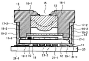
図1に示すように、第1の実施形態に係るカメラモジュールは、受動素子10及び撮像素子11が配置された絶縁基板12と、径大部16−1と、この下部に形成された径小部16−2からなる筒型の形状であり、レンズ13の上部に光入射用開口部15が形成されたレンズホルダ16とを有している。このレンズホルダ16には、内部にレンズ13及び赤外線カットフィルタ14が配置され、更にレンズホルダ16は、径小部16−2の下部と絶縁基板12との間に塗布される接着剤17−1によって固定されている。ここで筒型とは、断面が略円で管状の形状だけでなく、略円以外の形状、例えば多角形の形状の断面を有する管状の形状をも全て含む形状を指すが、本実施形態においては断面が略円で管状の形状である。以下、筒型は全て同様の意味を有する。
As shown in FIG. 1, the camera module according to the first embodiment includes an
このように絶縁基板12上に固定されたレンズホルダ16の径小部16−2は、導電用開口部18を有する板状の底部19−1と、底部19−1の外周部上に形成され、レンズホルダ16の径小部16−2に嵌合した筒型の形状の側部19−2と、を備えた有底筒状のシールド19に覆われている。そして、シールド19は、シールド19の上端部とレンズホルダの径大部16−1の下部との間に塗布された接着剤17−2によって固定されている。このシールド19は、例えば金属または、樹脂表面を導通性の膜で覆った導通性の樹脂によって形成されている。
The small-diameter portion 16-2 of the
このようなレンズホルダ16を内部に有するシールド19は、実装基板20上に形成された半田ペースト21−1によって実装基板20に固定されている。さらに、シールド19の内部の絶縁基板12の下には複数の半田ボール21−2が形成されている。一方で、実装基板20上には、これら複数の半田ボール21−2の位置に対応して半田ペースト21−1が形成されており、これら半田ボール21−2及び半田ペースト21−1を介して、絶縁基板12と実装基板20とは導通されている。
The shield 19 having such a
このようなカメラモジュールにおいて、シールド19は、シールドの底部19−1が絶縁基板12の下面に接するように固定されている。このようにシールド19を固定することにより、シールドの底部19−1の下面と半田ボール21−2の下部で決定される面の平坦度は、レンズホルダ16の高さ、絶縁基板12の厚さ、レンズホルダ16の径小部16−2の下部と絶縁基板12との間の接着剤17−1の厚さ、レンズホルダの径大部16−1の下部とシールド19の上端部との間の接着剤17−2の厚さに係らず、シールドの底部19−1の厚さのみで決定される。すなわち、レンズホルダ16の高さ及び絶縁基板12の厚さの製造誤差は、レンズホルダの径大部16−1の下部とシールド19の上端部との間の接着剤17−2の厚さで補償することができる。従って、従来のカメラモジュールと比較すると、シールドの底部19−1の下面と半田ボール21−2の下部で決定される面の平坦度を容易に制御することが可能となる。よって、シールド19を実装基板20に実装する際に、絶縁基板12の下に形成された半田ボール21−2及びシールド19は共に、容易に実装基板20に接することができる。
In such a camera module, the shield 19 is fixed so that the bottom 19-1 of the shield is in contact with the lower surface of the
また、上述したカメラモジュールは、撮像素子11が配置された絶縁基板12と実装基板20との間にシールドの底部19−1が形成されているため、絶縁基板12または実装基板20から出射される電磁波を、互いに遮断する効果もある。
Moreover, since the bottom 19-1 of the shield is formed between the
次に、本実施形態に係るカメラモジュールの製造方法について図2〜図4を参照して説明する。 Next, a method for manufacturing the camera module according to the present embodiment will be described with reference to FIGS.
はじめに、受動素子10及び撮像素子11が配置された絶縁基板12上の所定の位置に接着剤17−1を塗布し、塗布された接着剤17−1上にレンズホルダ16を配置する。このとき使用される接着剤17−1は、例えばUV硬化型接着剤または、これに熱硬化型接着剤を併用した接着剤である。
First, the adhesive 17-1 is applied to a predetermined position on the
次に、レンズホルダ16の径小部16−2の下部と絶縁基板12との間に塗布された接着剤17−1に紫外線を照射することでこの接着剤17−1を硬化させ、レンズホルダ16を絶縁基板12に固着させる。
Next, the adhesive 17-1 is cured by irradiating the adhesive 17-1 applied between the lower portion of the small-diameter portion 16-2 of the
次に、図2に示すように、レンズホルダ16が固着された絶縁基板12を上下方向に反転させ、絶縁基板12の下面の所定の位置に、複数の半田ボール21−2を形成する。このとき半田ボール21−2の高さは、後に配置されるシールドの底部19−1の高さよりも高くなるように形成する。一方で、実装基板20上の所定の位置には半田ペースト21−1を形成し、上下方向に反転させる。
Next, as shown in FIG. 2, the
次に、図3に示すように、シールドの底部19−1が絶縁基板12の下面に接するようにシールド19を配置し、シールド19の上部(上下反転した状態では下部)とレンズホルダの径大部16−1の下部(上下反転した状態では上部)との間に接着剤17−2を塗布する。このとき使用される接着剤17−2も、例えばUV硬化型接着剤または、これに熱硬化型接着剤を併用した接着剤である。
Next, as shown in FIG. 3, the shield 19 is arranged so that the bottom 19-1 of the shield is in contact with the lower surface of the
最後に、図4に示すように、シールドの底部19−1及び半田ボール21−2が実装基板20に形成された半田ペースト21−1に接するように、絶縁基板12が固着されたレンズホルダ16を下から押し当てる。さらに、下から押し当てたままシールド19の上部とレンズホルダの径大部16−1の下部との間に接着剤17−2に紫外線を照射し、硬化させることでレンズホルダ16をシールド19に固着させる。
Finally, as shown in FIG. 4, the
以上の工程によって、本実施形態に係るカメラモジュールを製造することができる。 The camera module according to the present embodiment can be manufactured through the above steps.
このように、シールドの底部19−1及び半田ボール21−2が実装基板20に形成された半田ペースト21−1に接した状態で、シールド19の上部とレンズホルダの径大部16−1の下部との間の接着剤17−2を硬化させるため、シールドの底部19−1の下面(上下反転した状態では上面)及び半田ボール21−2の下部(上下反転した状態では上部)とで決定される面を平坦にすることができる。さらに、シールドの底部19−1の下面と半田ボール21−2の下部で決定される面が完全に平坦ではなかった場合であっても、実装基板20上に形成された半田ペースト21−1に半田ボール21−2が埋もれるようにシールド19が固着されるため、平坦度を補償することが可能である。
Thus, in the state where the bottom 19-1 of the shield and the solder ball 21-2 are in contact with the solder paste 21-1 formed on the mounting
(第2の実施形態)
図5は、他の実施形態に係るカメラモジュールの構造断面図を示す。
(Second Embodiment)
FIG. 5 is a structural cross-sectional view of a camera module according to another embodiment.
図5に示すように、第2の実施形態に係るカメラモジュールは、接着剤17によって撮像素子11が裏面に固定されたガラス基板12´と、径大部16−1と、この下部に形成された径小部16−2からなる筒型の形状であり、レンズ13の上部に光入射用開口部15が形成されたレンズホルダ16とを有している。このレンズホルダ16には、内部にレンズ13及び赤外線カットフィルタ14が配置され、更にレンズホルダ16は、径小部16−2の下部とガラス基板12´との間に塗布される接着剤17−1によって固定されている。このようにガラス基板12´上に固定されたレンズホルダ16の径小部16−2は、導電用開口部18を有する板状の底部19−1と、底部19−1の外周部上に形成され、レンズホルダ16の径小部16−2に嵌合した筒型の形状の側部19−2と、を備えた有底筒状のシールド19に覆われている。そして、シールド19は、シールド19の上端部とレンズホルダの径大部16−1の下部との間に塗布された接着剤17−2によって固定されている。このシールド19は、例えば金属または、樹脂表面を導通性の膜で覆った導通性の樹脂によって形成されている。
As shown in FIG. 5, the camera module according to the second embodiment is formed in a
このようなレンズホルダ16を内部に有するシールド19は、実装基板20上に形成された半田ペースト21−1によって実装基板20に固定される。さらに、シールド19の内部の撮像素子11の下には複数の半田ボール21−2が形成されている。一方で、実装基板20上には、これら複数の半田ボール21−2の位置に対応して半田ペースト21−1が形成されており、これら半田ボール21−2及び半田ペースト20−1を介して、撮像素子11と実装基板20とは導通されている。
The shield 19 having such a
このような構造であっても、シールドの底部19−1は撮像素子11の下面に固定されるため、シールドの底部19−1と半田ボール21−2の下部で決定される面の平坦度は、レンズホルダ16の高さ、絶縁基板12の厚さ、レンズホルダ16の径小部16−2の下部とガラス基板12´との間に塗布される接着剤17−1の厚さ、シールド19の上端部とレンズホルダの径大部16−1の下部との間に塗布された接着剤17−2の厚さに係らず、シールドの底部19−1の厚さのみで決定される。従って、従来のカメラモジュールと比較して容易に平坦度を制御することが可能となる。よって、シールド19を実装基板20に実装する際に、撮像素子11の下に形成された半田ボール21−2及びシールド19は共に、容易に実装基板20に接することができる。
Even in such a structure, since the bottom 19-1 of the shield is fixed to the lower surface of the
また、上述したカメラモジュールは、撮像素子11と実装基板20との間にシールドの底部19−1が形成されているため、撮像素子11または実装基板20から出射される電磁波を、互いに遮断する効果もある。
Moreover, since the bottom 19-1 of the shield is formed between the
なお、第2の実施形態に係るカメラモジュールの製造方法に関しては、第1の実施形態に係るカメラモジュールの製造方法とほぼ変わらないため、ここでは説明を省略するが、第1の実施形態に係るカメラモジュールの製造方法と同様の効果を得ることが可能である。 Note that the manufacturing method of the camera module according to the second embodiment is not substantially different from the manufacturing method of the camera module according to the first embodiment, and thus the description thereof is omitted here, but according to the first embodiment. It is possible to obtain the same effect as the camera module manufacturing method.
以上は、レンズホルダ16が絶縁基板12または撮像素子11に直接固定されるようなカメラモジュールにおける一実施形態であった。しかし本発明は、レンズホルダ16がバレル22に保持され、このバレル22が絶縁基板12または撮像素子11に固定されるようなカメラモジュールにおいても適用可能である。以下に、レンズホルダ16がバレル22に保持され、このバレル22が絶縁基板12または撮像素子11に固定されるようなカメラモジュールの一実施形態について説明する。
The above is an embodiment of the camera module in which the
(第3の実施形態)
図6は、他の実施形態に係るカメラモジュールの構造断面図を示す。
(Third embodiment)
FIG. 6 is a structural cross-sectional view of a camera module according to another embodiment.
図6に示すように、第3の実施形態に係るカメラモジュールは、受動素子10及び撮像素子11が配置された絶縁基板12と、筒型の形状であり、レンズ13の上部に光入射用開口部15が形成されたレンズホルダ16と、径大部22−1及びこの径大部22−1の下部に形成された径小部22−2からなる筒型の形状のバレル22とを有している。レンズホルダ16には、内部にレンズ13が配置され、バレル22には、内部に赤外線カットフィルタ14が配置されている。このバレル22は内側部にネジ構造23が形成される一方で、レンズホルダ16の外側部にもネジ構造23が形成されており、これらのネジ構造23により、レンズホルダ16はバレル22に固定されている。さらに、バレル22は、バレル22の径小部22−2の下部と絶縁基板12との間に塗布された接着剤17−1によって絶縁基板12上に固定されている。このように絶縁基板12上に固定されたバレル22の径小部22−2は、導電用開口部18を有する板状の底部19−1と、底部19−1の外周部上に形成され、バレル22の径小部22−2に嵌合した筒型の形状の側部19−2と、を備えた有底筒状のシールド19に覆われている。そして、シールド19は、シールド19の上端部とバレルの径大部22−1の下部との間に塗布された接着剤17−2によって固定されている。このシールド19は、例えば金属または、樹脂表面を導通性の膜で覆った導通性の樹脂によって形成されている。
As shown in FIG. 6, the camera module according to the third embodiment has an insulating
このようなバレル22を内部に有するシールド19は、実装基板20上に形成された半田ペースト21−1によって実装基板20に固定されている。さらに、シールド19の内部の絶縁基板12の下には複数の半田ボール21−2が形成されている。一方で、実装基板20上には、これら複数の半田ボール21−2の位置に対応して半田ペースト21−1が形成されており、これら半田ボール21−2及び半田ペースト21−1を介して、絶縁基板12と実装基板20とは導通されている。
The shield 19 having such a
このようなカメラモジュールであっても、第1の実施形態に係るカメラモジュールと同様の効果を得ることができる。 Even with such a camera module, the same effects as those of the camera module according to the first embodiment can be obtained.
また、上述したカメラモジュールは、絶縁基板12と実装基板20との間にシールドの底部19−1が形成されているため、絶縁基板12または実装基板20から出射される電磁波を、互いに遮断する効果もある。
Moreover, since the bottom 19-1 of the shield is formed between the insulating
さらに、第3の実施形態に係るカメラモジュールの製造方法に関しては、第1の実施形態に係るカメラモジュールの組み立て工程とほぼ変わらないため、ここでは説明を省略する。 Furthermore, the method for manufacturing the camera module according to the third embodiment is not substantially different from the assembly process of the camera module according to the first embodiment, and thus the description thereof is omitted here.
以上に本発明の実施形態を示したが、実施形態はこれらに限るものではない。 Although the embodiments of the present invention have been described above, the embodiments are not limited thereto.
例えば、少なくともレンズ13を有するレンズホルダ16が、シールド19を介して実装基板20に固定されるカメラモジュールについては、全てにおいて適用可能である。
For example, the present invention can be applied to all camera modules in which the
また、上記の実施形態において、接着剤17、17−1、17−2は、硬化時間が早く、硬化後の変動が少ない点で製造に有利なUV硬化型接着剤または、これに熱硬化型接着剤を併用した接着剤が好ましい。しかし、接着剤17、17−1、17−2は他のどんな接着剤を用いても本発明の効果が失われるものではない。
In the above embodiment, the
10・・・受動素子
11・・・撮像素子
12・・・絶縁基板
12’・・・ガラス基板
13・・・レンズ
14・・・赤外線カットフィルタ
15・・・光入射用開口部
16・・・レンズホルダ
16−1・・・レンズホルダの径大部
16−2・・・レンズホルダの径小部
17・・・接着剤
17−1・・・レンズホルダ(バレル)の径小部の下部と絶縁基板との間の接着剤
17−2・・・レンズホルダ(バレル)の径大部の下部とシールドの上端部との間の接着剤
18・・・導電用開口部
19・・・シールド
19−1・・・シールドの底部
19−2・・・シールドの側部
20・・・実装基板
21−1・・・半田ペースト
21−2・・・半田ボール
22・・・バレル
22−1・・・バレルの径大部
22−2・・・バレルの径小部
23・・・ネジ構造
DESCRIPTION OF
Claims (11)
この絶縁基板または前記撮像素子の下面に形成された複数の半田ボールと、
前記絶縁基板上に固着され、上部径大部及び下部径小部からなる筒状のレンズホルダと、
このレンズホルダの前記径小部に嵌合し、前記レンズホルダの径大部に接着された筒状の側部および、前記絶縁基板または前記撮像素子の下面と接し、導電用開口部を有する板状の底部からなる有底筒状のシールドと、
前記複数の半田ボールを介して前記絶縁基板または前記撮像素子に接続され、前記シールドの前記底部に接する実装基板と、
を具備することを特徴とするカメラモジュール。 An insulating substrate having an image sensor;
A plurality of solder balls formed on the lower surface of the insulating substrate or the imaging element;
A cylindrical lens holder fixed on the insulating substrate and composed of a large upper diameter portion and a lower lower diameter portion;
A plate that fits into the small diameter portion of the lens holder and is in contact with the cylindrical side portion bonded to the large diameter portion of the lens holder and the lower surface of the insulating substrate or the imaging element, and has a conductive opening. A bottomed cylindrical shield consisting of a bottom of the shape,
A mounting substrate connected to the insulating substrate or the imaging element via the plurality of solder balls and in contact with the bottom of the shield;
A camera module comprising:
前記シールドは、前記レンズホルダの前記径大部の下面と前記シールドの上端部との間に塗布された接着剤により、前記レンズホルダに固着されることを特徴とする請求項1に記載のカメラモジュール。 The lens holder is fixed on the insulating substrate by an adhesive applied between the lower end of the small diameter portion of the lens holder and the insulating substrate,
The camera according to claim 1, wherein the shield is fixed to the lens holder by an adhesive applied between a lower surface of the large-diameter portion of the lens holder and an upper end portion of the shield. module.
この絶縁基板または前記撮像素子の下面に形成された複数の半田ボールと、
前記絶縁基板上に固着され、上部径大部及び下部径小部からなり、内側部にネジ構造を有する筒状のバレルと、
このバレルの内側部のネジ構造に対応したネジ構造を外側部に有し、これによって前記バレルに保持されるレンズホルダと、
前記バレルの前記径小部に嵌合し、前記バレルの径大部に接着された筒状の側部および、前記絶縁基板または前記撮像素子の下面と接し、導電用開口部を有する板状の底部からなる有底筒状のシールドと、
前記複数の半田ボールを介して前記絶縁基板または前記撮像素子に接続され、前記シールドの前記底部に接続する実装基板と、
を具備することを特徴とするカメラモジュール。 An insulating substrate having an image sensor;
A plurality of solder balls formed on the lower surface of the insulating substrate or the imaging element;
A cylindrical barrel fixed on the insulating substrate, consisting of an upper diameter large portion and a lower diameter small portion, and having a screw structure on the inner side;
A lens holder corresponding to the screw structure of the inner part of the barrel on the outer part, thereby holding the lens holder on the barrel;
A plate-like shape that fits into the small diameter portion of the barrel and is in contact with the cylindrical side portion bonded to the large diameter portion of the barrel and the lower surface of the insulating substrate or the imaging element, and has a conductive opening. A bottomed cylindrical shield consisting of the bottom,
A mounting substrate connected to the insulating substrate or the imaging element via the plurality of solder balls and connected to the bottom of the shield;
A camera module comprising:
前記シールドは、前記バレルの前記径大部の下面と前記シールドの上端部との間に塗布された接着剤により、前記バレルに固着されることを特徴とする請求項3に記載のカメラモジュール。 The barrel is fixed on the insulating substrate by an adhesive applied between the lower end of the small diameter portion of the barrel and the insulating substrate,
The camera module according to claim 3, wherein the shield is fixed to the barrel by an adhesive applied between a lower surface of the large-diameter portion of the barrel and an upper end portion of the shield.
前記撮像素子は、前記ガラス基板の裏面に固定されたことを特徴とする請求項1乃至7のいずれかに記載のカメラモジュール。 The insulating substrate is a glass substrate;
The imaging device includes a camera module according to any one of claims 1 to 7, characterized in that it is fixed to the back surface of the glass substrate.
この工程により前記絶縁基板上に固定された前記レンズホルダを上下反転させた後に、前記絶縁基板または前記撮像素子の下面に複数の半田ボールを形成する工程と、
前記レンズホルダの前記径小部に嵌合する筒状の側部および、導電用開口部を有する板状の底部からなるシールドの前記底部が、前記絶縁基板または前記撮像素子の下面に接するように前記シールドを配置し、この配置された前記シールドの側部上端と前記レンズホルダ径大部の下面との間に、第2の接着剤を塗布する工程と、
前記シールドの前記底部を実装基板と前記絶縁基板または前記撮像素子との間にはさみこむように、前記実装基板の表面に前記絶縁基板を押し当てる工程と、
前記実装基板と前記絶縁基板または前記撮像素子との間に前記シールドの前記底部がはさみこまれた状態で、前記第2の接着剤を硬化させる工程と、
を具備することを特徴とするカメラモジュールの製造方法。 By applying a first adhesive between an insulating substrate having an image pickup element and a lower end of a lens holder having an upper diameter large portion and a lower diameter small portion, and having a lens inside, on the insulating substrate Fixing the lens holder;
A step of forming a plurality of solder balls on the lower surface of the insulating substrate or the imaging element after the lens holder fixed on the insulating substrate is turned upside down by this step;
The bottom portion of the shield, which is formed of a cylindrical side portion that fits into the small-diameter portion of the lens holder and a plate-like bottom portion having a conductive opening, is in contact with the lower surface of the insulating substrate or the imaging element. Arranging the shield, and applying a second adhesive between the upper side of the arranged shield and the lower surface of the large diameter part of the lens holder;
Pressing the insulating substrate against the surface of the mounting substrate so that the bottom of the shield is sandwiched between the mounting substrate and the insulating substrate or the imaging element;
Curing the second adhesive with the bottom of the shield sandwiched between the mounting substrate and the insulating substrate or the imaging element;
A method of manufacturing a camera module.
Priority Applications (3)
| Application Number | Priority Date | Filing Date | Title |
|---|---|---|---|
| JP2008095176A JP4762264B2 (en) | 2008-04-01 | 2008-04-01 | Camera module and camera module manufacturing method |
| US12/415,409 US7876513B2 (en) | 2008-04-01 | 2009-03-31 | Camera module and method for manufacturing the same |
| US12/964,450 US8164841B2 (en) | 2008-04-01 | 2010-12-09 | Camera module |
Applications Claiming Priority (1)
| Application Number | Priority Date | Filing Date | Title |
|---|---|---|---|
| JP2008095176A JP4762264B2 (en) | 2008-04-01 | 2008-04-01 | Camera module and camera module manufacturing method |
Publications (3)
| Publication Number | Publication Date |
|---|---|
| JP2009253363A JP2009253363A (en) | 2009-10-29 |
| JP2009253363A5 JP2009253363A5 (en) | 2011-03-03 |
| JP4762264B2 true JP4762264B2 (en) | 2011-08-31 |
Family
ID=41116800
Family Applications (1)
| Application Number | Title | Priority Date | Filing Date |
|---|---|---|---|
| JP2008095176A Expired - Fee Related JP4762264B2 (en) | 2008-04-01 | 2008-04-01 | Camera module and camera module manufacturing method |
Country Status (2)
| Country | Link |
|---|---|
| US (2) | US7876513B2 (en) |
| JP (1) | JP4762264B2 (en) |
Families Citing this family (16)
| Publication number | Priority date | Publication date | Assignee | Title |
|---|---|---|---|---|
| JP2011023889A (en) * | 2009-07-14 | 2011-02-03 | Fujifilm Corp | Imaging module and method of adjusting imaging |
| KR101081997B1 (en) * | 2009-12-04 | 2011-11-09 | 삼성전기주식회사 | Camera module |
| KR20110063158A (en) * | 2009-12-04 | 2011-06-10 | 삼성전기주식회사 | Camera module |
| JP5482231B2 (en) * | 2010-01-26 | 2014-05-07 | 株式会社リコー | Imaging device |
| JP5017406B2 (en) * | 2010-03-24 | 2012-09-05 | 株式会社東芝 | The camera module |
| KR101128931B1 (en) * | 2010-08-11 | 2012-03-27 | 삼성전기주식회사 | Camera module |
| JP5682185B2 (en) * | 2010-09-07 | 2015-03-11 | ソニー株式会社 | Semiconductor package, semiconductor package manufacturing method, and optical module |
| JP2012242587A (en) * | 2011-05-19 | 2012-12-10 | Toshiba Corp | Camera module and manufacturing method of camera module |
| US20130083229A1 (en) * | 2011-09-30 | 2013-04-04 | Omnivision Technologies, Inc. | Emi shield for camera module |
| JP6328799B2 (en) * | 2015-01-19 | 2018-05-23 | シャープ株式会社 | Manufacturing method of camera module and camera module |
| US10070028B2 (en) * | 2016-02-10 | 2018-09-04 | Microsoft Technology Licensing, Llc | Optical systems and methods of use |
| US11019243B2 (en) | 2017-05-30 | 2021-05-25 | Sony Semiconductor Solutions Corporation | Camera unit and mobile body |
| JP6730239B2 (en) * | 2017-09-27 | 2020-07-29 | 京セラ株式会社 | Imaging device, manufacturing method of imaging device, and moving body |
| TWI728467B (en) * | 2019-09-17 | 2021-05-21 | 大陽科技股份有限公司 | Camera module and electronic device |
| CN114460789A (en) * | 2020-11-02 | 2022-05-10 | 阿尔卑斯阿尔派株式会社 | Lens driving device and camera module |
| DE102021209301A1 (en) | 2021-08-25 | 2023-03-02 | Robert Bosch Gesellschaft mit beschränkter Haftung | Image capture device and method for manufacturing an image capture device |
Family Cites Families (6)
| Publication number | Priority date | Publication date | Assignee | Title |
|---|---|---|---|---|
| JP4292383B2 (en) * | 2003-05-19 | 2009-07-08 | セイコーエプソン株式会社 | Optical device manufacturing method |
| JP2005229431A (en) | 2004-02-13 | 2005-08-25 | Toshiba Corp | Camera module of electronic apparatus |
| JP4407339B2 (en) * | 2004-03-26 | 2010-02-03 | パナソニック株式会社 | Imaging device |
| JP2007288755A (en) * | 2006-04-14 | 2007-11-01 | Optopac Co Ltd | Camera module |
| JP4799543B2 (en) * | 2007-12-27 | 2011-10-26 | 株式会社東芝 | Semiconductor package and camera module |
| JP4946921B2 (en) * | 2008-03-05 | 2012-06-06 | ソニー株式会社 | The camera module |
-
2008
- 2008-04-01 JP JP2008095176A patent/JP4762264B2/en not_active Expired - Fee Related
-
2009
- 2009-03-31 US US12/415,409 patent/US7876513B2/en not_active Expired - Fee Related
-
2010
- 2010-12-09 US US12/964,450 patent/US8164841B2/en active Active
Also Published As
| Publication number | Publication date |
|---|---|
| US7876513B2 (en) | 2011-01-25 |
| US20090244728A1 (en) | 2009-10-01 |
| US20110076007A1 (en) | 2011-03-31 |
| JP2009253363A (en) | 2009-10-29 |
| US8164841B2 (en) | 2012-04-24 |
Similar Documents
| Publication | Publication Date | Title |
|---|---|---|
| JP4762264B2 (en) | Camera module and camera module manufacturing method | |
| JP2009253363A5 (en) | ||
| KR102384157B1 (en) | semiconductor package and method for manufacturing of the same | |
| JP2010191345A (en) | Lens unit, camera module, and method for manufacturing lens unit | |
| TW202017358A (en) | Camera module, and photosensitive component thereof and manufacturing method therefor | |
| KR20190113856A (en) | Photographing module and mold photosensitive assembly and manufacturing method thereof, and electronic device | |
| JP2007299929A (en) | Optical device, and optical device module employing it | |
| JP2003283890A (en) | Imaging apparatus and manufacturing method of imaging apparatus | |
| JP2007184801A (en) | Camera module | |
| US8699154B2 (en) | Camera lens assembly and producing method thereof | |
| JP2010219713A (en) | Imaging device | |
| JP2013118230A (en) | Solid-state imaging device | |
| JP2007206337A (en) | Manufacturing method of optical module | |
| JP2007206336A (en) | Optical module and manufacturing method thereof | |
| JP2005260436A (en) | Imaging module and imaging apparatus employing it | |
| US20200186684A1 (en) | Circuit board assembly, camera module, and electronic device including the same | |
| JP2009141406A (en) | Method for manufacturing camera module | |
| TWI589946B (en) | Lens focusing method and optical module | |
| TWM470285U (en) | Image capturing module and image sensing unit | |
| WO2017134972A1 (en) | Imaging element package and imaging device | |
| TWI564610B (en) | Camera module and method for fabricating the same | |
| KR20180130168A (en) | Camera module and method of manufacturing it | |
| JP2011165774A (en) | Production method of solid-state image pickup device | |
| JP2005242242A (en) | Image sensor package and camera module | |
| JP2005229088A (en) | Optical device, method of manufacturing the same, cap component, and method of manufacturing the same |
Legal Events
| Date | Code | Title | Description |
|---|---|---|---|
| A621 | Written request for application examination |
Free format text: JAPANESE INTERMEDIATE CODE: A621 Effective date: 20100728 |
|
| A521 | Request for written amendment filed |
Free format text: JAPANESE INTERMEDIATE CODE: A523 Effective date: 20110114 |
|
| A871 | Explanation of circumstances concerning accelerated examination |
Free format text: JAPANESE INTERMEDIATE CODE: A871 Effective date: 20110114 |
|
| A975 | Report on accelerated examination |
Free format text: JAPANESE INTERMEDIATE CODE: A971005 Effective date: 20110131 |
|
| A131 | Notification of reasons for refusal |
Free format text: JAPANESE INTERMEDIATE CODE: A131 Effective date: 20110208 |
|
| A521 | Request for written amendment filed |
Free format text: JAPANESE INTERMEDIATE CODE: A523 Effective date: 20110223 |
|
| A01 | Written decision to grant a patent or to grant a registration (utility model) |
Free format text: JAPANESE INTERMEDIATE CODE: A01 Effective date: 20110510 |
|
| A61 | First payment of annual fees (during grant procedure) |
Free format text: JAPANESE INTERMEDIATE CODE: A61 Effective date: 20110607 |
|
| FPAY | Renewal fee payment (event date is renewal date of database) |
Free format text: PAYMENT UNTIL: 20140617 Year of fee payment: 3 |
|
| R150 | Certificate of patent or registration of utility model |
Free format text: JAPANESE INTERMEDIATE CODE: R150 |
|
| LAPS | Cancellation because of no payment of annual fees |