JP2017183668A - Manufacturing method for solid-state image pickup device - Google Patents
Manufacturing method for solid-state image pickup device Download PDFInfo
- Publication number
- JP2017183668A JP2017183668A JP2016073178A JP2016073178A JP2017183668A JP 2017183668 A JP2017183668 A JP 2017183668A JP 2016073178 A JP2016073178 A JP 2016073178A JP 2016073178 A JP2016073178 A JP 2016073178A JP 2017183668 A JP2017183668 A JP 2017183668A
- Authority
- JP
- Japan
- Prior art keywords
- gate electrode
- insulating film
- film
- peripheral circuit
- forming
- Prior art date
- Legal status (The legal status is an assumption and is not a legal conclusion. Google has not performed a legal analysis and makes no representation as to the accuracy of the status listed.)
- Pending
Links
- 238000004519 manufacturing process Methods 0.000 title claims abstract description 28
- 230000002093 peripheral effect Effects 0.000 claims abstract description 73
- 239000004065 semiconductor Substances 0.000 claims abstract description 68
- 238000000034 method Methods 0.000 claims abstract description 29
- 238000005530 etching Methods 0.000 claims abstract description 20
- UFHFLCQGNIYNRP-UHFFFAOYSA-N Hydrogen Chemical compound [H][H] UFHFLCQGNIYNRP-UHFFFAOYSA-N 0.000 claims description 32
- 229910052739 hydrogen Inorganic materials 0.000 claims description 32
- 239000001257 hydrogen Substances 0.000 claims description 32
- 229910052581 Si3N4 Inorganic materials 0.000 claims description 30
- HQVNEWCFYHHQES-UHFFFAOYSA-N silicon nitride Chemical compound N12[Si]34N5[Si]62N3[Si]51N64 HQVNEWCFYHHQES-UHFFFAOYSA-N 0.000 claims description 30
- 238000003384 imaging method Methods 0.000 claims description 29
- VYPSYNLAJGMNEJ-UHFFFAOYSA-N Silicium dioxide Chemical compound O=[Si]=O VYPSYNLAJGMNEJ-UHFFFAOYSA-N 0.000 claims description 18
- 229910052814 silicon oxide Inorganic materials 0.000 claims description 18
- 238000001312 dry etching Methods 0.000 claims description 16
- 239000002184 metal Substances 0.000 claims description 7
- 229910052751 metal Inorganic materials 0.000 claims description 7
- 239000000463 material Substances 0.000 claims description 6
- 229910021332 silicide Inorganic materials 0.000 claims description 5
- FVBUAEGBCNSCDD-UHFFFAOYSA-N silicide(4-) Chemical compound [Si-4] FVBUAEGBCNSCDD-UHFFFAOYSA-N 0.000 claims description 5
- 239000012212 insulator Substances 0.000 claims description 3
- 238000001039 wet etching Methods 0.000 claims description 3
- MROCJMGDEKINLD-UHFFFAOYSA-N dichlorosilane Chemical compound Cl[SiH2]Cl MROCJMGDEKINLD-UHFFFAOYSA-N 0.000 claims description 2
- LXEXBJXDGVGRAR-UHFFFAOYSA-N trichloro(trichlorosilyl)silane Chemical compound Cl[Si](Cl)(Cl)[Si](Cl)(Cl)Cl LXEXBJXDGVGRAR-UHFFFAOYSA-N 0.000 claims description 2
- 238000009413 insulation Methods 0.000 abstract 3
- 239000010410 layer Substances 0.000 description 27
- 229910021420 polycrystalline silicon Inorganic materials 0.000 description 19
- 229920005591 polysilicon Polymers 0.000 description 19
- 238000006243 chemical reaction Methods 0.000 description 10
- 230000015572 biosynthetic process Effects 0.000 description 9
- 238000005468 ion implantation Methods 0.000 description 9
- 239000000758 substrate Substances 0.000 description 8
- 239000012535 impurity Substances 0.000 description 7
- BOTDANWDWHJENH-UHFFFAOYSA-N Tetraethyl orthosilicate Chemical compound CCO[Si](OCC)(OCC)OCC BOTDANWDWHJENH-UHFFFAOYSA-N 0.000 description 4
- 239000011229 interlayer Substances 0.000 description 4
- 238000004518 low pressure chemical vapour deposition Methods 0.000 description 4
- 238000005268 plasma chemical vapour deposition Methods 0.000 description 4
- 238000002955 isolation Methods 0.000 description 3
- PXHVJJICTQNCMI-UHFFFAOYSA-N Nickel Chemical compound [Ni] PXHVJJICTQNCMI-UHFFFAOYSA-N 0.000 description 2
- 238000004380 ashing Methods 0.000 description 2
- 238000009792 diffusion process Methods 0.000 description 2
- 230000003287 optical effect Effects 0.000 description 2
- 229920002120 photoresistant polymer Polymers 0.000 description 2
- DYCJFJRCWPVDHY-LSCFUAHRSA-N NBMPR Chemical compound O[C@@H]1[C@H](O)[C@@H](CO)O[C@H]1N1C2=NC=NC(SCC=3C=CC(=CC=3)[N+]([O-])=O)=C2N=C1 DYCJFJRCWPVDHY-LSCFUAHRSA-N 0.000 description 1
- 238000000137 annealing Methods 0.000 description 1
- 239000005380 borophosphosilicate glass Substances 0.000 description 1
- 229910017052 cobalt Inorganic materials 0.000 description 1
- 239000010941 cobalt Substances 0.000 description 1
- GUTLYIVDDKVIGB-UHFFFAOYSA-N cobalt atom Chemical compound [Co] GUTLYIVDDKVIGB-UHFFFAOYSA-N 0.000 description 1
- 239000004020 conductor Substances 0.000 description 1
- 230000007547 defect Effects 0.000 description 1
- 238000000151 deposition Methods 0.000 description 1
- 230000008021 deposition Effects 0.000 description 1
- 230000006866 deterioration Effects 0.000 description 1
- 239000011521 glass Substances 0.000 description 1
- 238000010438 heat treatment Methods 0.000 description 1
- 238000002513 implantation Methods 0.000 description 1
- 238000010849 ion bombardment Methods 0.000 description 1
- 229910052759 nickel Inorganic materials 0.000 description 1
- 230000003647 oxidation Effects 0.000 description 1
- 238000007254 oxidation reaction Methods 0.000 description 1
- 230000001737 promoting effect Effects 0.000 description 1
- 229910052710 silicon Inorganic materials 0.000 description 1
- 239000010703 silicon Substances 0.000 description 1
- 238000005011 time of flight secondary ion mass spectroscopy Methods 0.000 description 1
- 238000002042 time-of-flight secondary ion mass spectrometry Methods 0.000 description 1
Images
Classifications
-
- H—ELECTRICITY
- H01—ELECTRIC ELEMENTS
- H01L—SEMICONDUCTOR DEVICES NOT COVERED BY CLASS H10
- H01L27/00—Devices consisting of a plurality of semiconductor or other solid-state components formed in or on a common substrate
- H01L27/14—Devices consisting of a plurality of semiconductor or other solid-state components formed in or on a common substrate including semiconductor components sensitive to infrared radiation, light, electromagnetic radiation of shorter wavelength or corpuscular radiation and specially adapted either for the conversion of the energy of such radiation into electrical energy or for the control of electrical energy by such radiation
- H01L27/144—Devices controlled by radiation
- H01L27/146—Imager structures
- H01L27/14683—Processes or apparatus peculiar to the manufacture or treatment of these devices or parts thereof
- H01L27/14689—MOS based technologies
-
- H—ELECTRICITY
- H01—ELECTRIC ELEMENTS
- H01L—SEMICONDUCTOR DEVICES NOT COVERED BY CLASS H10
- H01L27/00—Devices consisting of a plurality of semiconductor or other solid-state components formed in or on a common substrate
- H01L27/14—Devices consisting of a plurality of semiconductor or other solid-state components formed in or on a common substrate including semiconductor components sensitive to infrared radiation, light, electromagnetic radiation of shorter wavelength or corpuscular radiation and specially adapted either for the conversion of the energy of such radiation into electrical energy or for the control of electrical energy by such radiation
- H01L27/144—Devices controlled by radiation
- H01L27/146—Imager structures
- H01L27/14601—Structural or functional details thereof
- H01L27/14609—Pixel-elements with integrated switching, control, storage or amplification elements
- H01L27/14612—Pixel-elements with integrated switching, control, storage or amplification elements involving a transistor
- H01L27/14614—Pixel-elements with integrated switching, control, storage or amplification elements involving a transistor having a special gate structure
-
- H—ELECTRICITY
- H01—ELECTRIC ELEMENTS
- H01L—SEMICONDUCTOR DEVICES NOT COVERED BY CLASS H10
- H01L29/00—Semiconductor devices adapted for rectifying, amplifying, oscillating or switching, or capacitors or resistors with at least one potential-jump barrier or surface barrier, e.g. PN junction depletion layer or carrier concentration layer; Details of semiconductor bodies or of electrodes thereof ; Multistep manufacturing processes therefor
- H01L29/40—Electrodes ; Multistep manufacturing processes therefor
- H01L29/43—Electrodes ; Multistep manufacturing processes therefor characterised by the materials of which they are formed
- H01L29/45—Ohmic electrodes
-
- H—ELECTRICITY
- H01—ELECTRIC ELEMENTS
- H01L—SEMICONDUCTOR DEVICES NOT COVERED BY CLASS H10
- H01L29/00—Semiconductor devices adapted for rectifying, amplifying, oscillating or switching, or capacitors or resistors with at least one potential-jump barrier or surface barrier, e.g. PN junction depletion layer or carrier concentration layer; Details of semiconductor bodies or of electrodes thereof ; Multistep manufacturing processes therefor
- H01L29/66—Types of semiconductor device ; Multistep manufacturing processes therefor
- H01L29/66007—Multistep manufacturing processes
- H01L29/66075—Multistep manufacturing processes of devices having semiconductor bodies comprising group 14 or group 13/15 materials
- H01L29/66227—Multistep manufacturing processes of devices having semiconductor bodies comprising group 14 or group 13/15 materials the devices being controllable only by the electric current supplied or the electric potential applied, to an electrode which does not carry the current to be rectified, amplified or switched, e.g. three-terminal devices
- H01L29/66409—Unipolar field-effect transistors
- H01L29/66477—Unipolar field-effect transistors with an insulated gate, i.e. MISFET
- H01L29/665—Unipolar field-effect transistors with an insulated gate, i.e. MISFET using self aligned silicidation, i.e. salicide
Abstract
Description
本発明は、固体撮像装置の製造方法に関する。 The present invention relates to a method for manufacturing a solid-state imaging device.
固体撮像装置において、画素領域での白点キズや暗電流などのノイズの原因の1つとして、半導体基板と半導体基板に接する絶縁膜との界面に形成される界面準位(ダングリングボンド)がある。このダングリングボンド起因のノイズを低減するために画素領域の上に水素供給膜を配し、画素領域に形成されたフォトダイオードなどの受光素子の表面のダングリングボンドを水素供給膜から供給される水素によって終端させることが特許文献1に示されている。特許文献1の製造方法では、基板の画素領域及び周辺回路領域となるそれぞれの部分にゲート電極を形成した後、基板を覆うように絶縁膜を形成し、この絶縁膜をエッチバックすることによってゲート電極の側壁にサイドウォールを形成する。次いで、基板を覆うように水素供給膜を形成し、水素供給膜のうち画素領域の上に配された部分を残し、周辺回路領域の上に配された部分をエッチングによって除去する。画素領域の上に配された水素供給膜によって、画素領域の受光素子に水素を供給することができる。
In solid-state imaging devices, one of the causes of noise such as white spot scratches and dark current in the pixel region is an interface state (dangling bond) formed at the interface between the semiconductor substrate and the insulating film in contact with the semiconductor substrate. is there. In order to reduce noise caused by this dangling bond, a hydrogen supply film is provided on the pixel region, and the dangling bond on the surface of the light receiving element such as a photodiode formed in the pixel region is supplied from the hydrogen supply film.
特許文献1に示される製造方法では、ゲート電極の形成や水素供給膜のうち周辺回路領域の上に配された部分の除去などを行うためのドライエッチングにおいて、半導体層にプラズマダメージなどのダメージが生じる可能性がある。周辺回路領域の半導体層にダメージが生じた場合、周辺回路領域に配されたトランジスタの接合リークの増大などトランジスタの特性がばらつく可能性がある。トランジスタの特性ばらつきは、固体撮像装置を製造する際の歩留まりを低下させる要因となりうる。
In the manufacturing method disclosed in
本発明は、固体撮像装置において周辺回路領域に配されたトランジスタの特性のばらつきを抑制するのに有利な技術を提供することを目的とする。 An object of the present invention is to provide a technique advantageous in suppressing variation in characteristics of transistors arranged in a peripheral circuit region in a solid-state imaging device.
上記課題に鑑みて、本発明の実施形態に係る固体撮像装置の製造方法は、画素領域及び周辺回路領域が半導体層に配された固体撮像装置の製造方法であって、半導体層の上にゲート電極膜を成膜する工程と、ゲート電極膜をエッチングし、周辺回路領域にゲート電極膜を残存させるとともに、画素領域にパターニングされた第1のゲート電極を形成する工程と、第1のゲート電極を形成する工程の後に、半導体層の上に第1の絶縁膜を成膜する工程と、周辺回路領域に形成された第1の絶縁膜を除去する工程と、第1の絶縁膜を除去する工程の後に、周辺回路領域に残存していたゲート電極膜をエッチングし、周辺回路領域にパターニングされた第2のゲート電極を形成する工程と、を含むことを特徴とする。 In view of the above problems, a method for manufacturing a solid-state imaging device according to an embodiment of the present invention is a method for manufacturing a solid-state imaging device in which a pixel region and a peripheral circuit region are arranged in a semiconductor layer, and a gate is formed on the semiconductor layer. Forming an electrode film; etching the gate electrode film to leave a gate electrode film in the peripheral circuit region; and forming a patterned first gate electrode in the pixel region; After the step of forming, a step of forming a first insulating film on the semiconductor layer, a step of removing the first insulating film formed in the peripheral circuit region, and removing the first insulating film A step of etching the gate electrode film remaining in the peripheral circuit region after the step to form a second gate electrode patterned in the peripheral circuit region.
上記手段によって、固体撮像装置において周辺回路領域に配されたトランジスタの特性のばらつきを抑制するのに有利な技術が提供される。 By the above means, a technique advantageous for suppressing variation in characteristics of transistors arranged in the peripheral circuit region in the solid-state imaging device is provided.
以下、本発明に係る固体撮像装置の具体的な実施形態を、添付図面を参照して説明する。なお、以下の説明及び図面において、複数の図面に渡って共通の構成については共通の符号を付している。そのため、複数の図面を相互に参照して共通する構成を説明し、共通の符号を付した構成については適宜説明を省略する。 Hereinafter, specific embodiments of a solid-state imaging device according to the present invention will be described with reference to the accompanying drawings. Note that, in the following description and drawings, common reference numerals are given to common configurations over a plurality of drawings. Therefore, a common configuration is described with reference to a plurality of drawings, and a description of a configuration with a common reference numeral is omitted as appropriate.
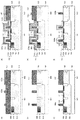
図1、2を参照して、本発明の実施形態による固体撮像装置の構造及び製造方法について説明する。図1、2は、本発明の実施形態における固体撮像装置の製造方法の各工程を示す断面図である。説明のため、図1、2では、画素領域101と周辺回路領域102とを隣接させて描いている。また、固体撮像装置の形成される半導体層100をn型の導電型の半導体領域として説明するが、以下に説明する各構成要素の導電型を含め、導電型はそれぞれ逆の導電型であってもよい。
With reference to FIGS. 1 and 2, the structure and manufacturing method of the solid-state imaging device according to the embodiment of the present invention will be described. 1 and 2 are cross-sectional views illustrating each step of a method for manufacturing a solid-state imaging device according to an embodiment of the present invention. 1 and 2, the
固体撮像装置は、半導体層100及び半導体層100の上に形成される。半導体層100は、シリコンなどのn型の半導体基板であってもよいし、半導体基板に設けられたn型のウェルであってもよい。また例えば、ガラスやプラスチックなどの絶縁基板上に設けられたn型の半導体層であってもよい。
The solid-state imaging device is formed on the
まず、半導体層100には、図1(a)に示すように、STIや選択酸化法(LOCOS)などによって形成された素子分離領域103、画素領域101及び周辺回路領域102に形成されたp型のウェル104、105が、それぞれ配される。また、画素領域101には、n型の半導体領域106が配される。半導体領域106は、ウェル104とpn接合を構成し、光電変換部として機能する。素子分離領域103、ウェル104、105、半導体領域106の形成後、ゲート絶縁膜(不図示)、及び、ゲート電極を形成するためのゲート電極膜としてポリシリコン膜107を半導体層100上に成膜する。素子分離領域103、ウェル104、105、半導体領域106、ゲート絶縁膜、及び、ポリシリコン膜107のそれぞれは、既知の製造方法にて形成することができる。
First, as shown in FIG. 1A, the
ポリシリコン膜107を形成した後、図1(a)に示すように、ポリシリコン膜107のうち画素領域101のゲート電極となる部分、及び、周辺回路領域102の上に配された部分を覆うマスクパターン122aを形成する。マスクパターン122aには、例えばフォトレジストなどが用いられる。次いで、形成されたマスクパターン122aに覆われない開口部を通してポリシリコン膜107をドライエッチングし、図1(b)に示すように、画素領域101にパターニングされたトランジスタのゲート電極108aを形成する。この工程によって、周辺回路領域102のポリシリコン膜107は加工されずに残存するとともに、画素領域101のトランジスタのゲート電極108aが形成される。周辺回路領域102は、ポリシリコン膜107及びマスクパターンによって覆われているため、周辺回路領域102の半導体層100に対するドライエッチングによるプラズマダメージを抑制できる。このドライエッチングを行う際のマスクパターンに、フォトレジストだけでなく酸化シリコンなどの絶縁膜を用いたハードマスクを使用してもよい。ドライエッチング後、マスクパターン122aは除去してもよいし、残存させておいてもよい。マスクパターン122aを周辺回路領域102に残存させた場合には、その後のイオン注入工程におけるダメージが半導体層100に入るのを抑制することができる。
After forming the
次いで、図1(c)に示すように、フローティングディフュージョン部となるn型の半導体領域110、画素領域101のトランジスタのソース・ドレイン領域となるn型の半導体領域111を、イオン注入法によって不純物を注入し形成する。また、図1(c)に示す構成のように、半導体領域106を埋め込み構造とするために、半導体領域106よりも浅い領域にp型の半導体領域109をイオン注入法によって形成してもよい。半導体領域109、110、111を形成する順番は、上述の順番に限られることはなく、適宜、形成すればよい。また、半導体領域106もポリシリコン膜107の成膜前でなく、ゲート電極108aの形成後に形成してもよい。マスクパターン122aをイオン注入工程前に除去した場合であっても、周辺回路領域102はポリシリコン膜107に覆われているため、不純物を注入する際のイオン衝撃に起因するダメージが抑制される。半導体領域109、110、111を形成した後、イオン注入による注入欠陥を回復するために700℃〜1100℃程度の熱処理を行ってもよい。
Next, as shown in FIG. 1C, the n-
半導体領域109、110、111の形成後、画素領域101及び周辺回路領域102を覆うように、半導体層100の上に絶縁膜112を成膜する。本実施形態において、絶縁膜112は、酸化シリコン膜112aと、酸化シリコン膜112aの上に配された窒化シリコン膜112bとを含む。酸化シリコン膜112aは、例えばテトラエトキシシラン(TEOS)を含む材料を用いて減圧CVD法によって形成される。窒化シリコン膜112bは、例えばジクロロシランやヘキサクロロジシランを含む材料を用いてプラズマCVD法によって形成される。これらの材料を用いてプラズマCVD法によって形成された窒化シリコンは、膜中に水素を多く含む水素供給膜として機能しうる。画素領域101の上に窒化シリコン膜112bを含む絶縁膜112を形成することによって、窒化シリコン膜112bから画素領域101に生成されたダングリングボンドに水素を供給し、ダングリングボンドを水素終端することができる。これによって、画素領域101の光電変換部やトランジスタで発生するノイズを低減することができる。本実施形態において、窒化シリコン膜112bの形成はプラズマCVDで行ったが、減圧CVDでもよい。また、本実施形態において、絶縁膜112は、酸化シリコン膜112aと窒化シリコン膜112bとの2層の積層構造を有するが、例えば、窒化シリコン膜112bの上に更に酸化シリコン膜を形成した3層構造であってもよい。
After the formation of the
次いで、図1(d)に示すように、絶縁膜112の形成後、画素領域101に配された絶縁膜112のうち少なくとも半導体領域106の形成された光電変換部を覆うマスクパターン122bを形成する。本実施形態において、絶縁膜112のうち画素領域101の上に配された部分全体を覆うマスクパターン122bを形成する。次いで、形成されたマスクパターン122bに覆われない開口部を通して、酸化シリコン膜112a及び窒化シリコン膜112bを含む絶縁膜112をエッチングする。このエッチングによって、周辺回路領域に形成された絶縁膜112が除去される。酸化シリコン膜112a及び窒化シリコン膜112bをドライエッチングによってエッチングしてもよい。また、窒化シリコン膜112bを等方性のドライエッチングによって除去した後、酸化シリコン膜112aをウエットエッチングによって除去してもよい。ドライエッチングとウエットエッチングとを組み合わせることによって、周辺回路領域102上のポリシリコン膜の側壁に絶縁膜112によるサイドウォールを形成することなく、絶縁膜112を除去することができる。本実施形態において、画素領域101全体を覆うマスクパターン122bによって、画素領域101の全体を覆うように絶縁膜112が残存する。
Next, as illustrated in FIG. 1D, after the formation of the insulating
この周辺回路領域102上の絶縁膜112をエッチングする工程において、画素領域101はマスクパターン122b及び絶縁膜112によって覆われている。このため、画素領域101の半導体層100へのドライエッチングによるプラズマダメージを抑制することができる。また、マスクパターン122bのアッシングなどによる除去及びマスクパターン122bを除去した後も、画素領域101上に絶縁膜112が残存する。このため、絶縁膜112を成膜する工程の後に行われる工程、例えば、周辺回路領域102の各構成要素を形成するためのイオン注入やドライエッチング、アッシングなどの工程によって生じる画素領域101の半導体層100へのダメージを抑制することができる。結果として、画素領域101の光電変換部で発生するノイズやトランジスタの特性のばらつきを抑制できる。マスクパターン122bが、画素領域101のうち光電変換部の上の部分のみを覆う場合であっても、以降の工程において、光電変換部が絶縁膜112によって覆われるため、光電変換部で発生するノイズを抑制できる。
In the step of etching the insulating
また、周辺回路領域102上の絶縁膜112をエッチングする工程において、周辺回路領域102は、ポリシリコン膜107によって覆われている。このため、画素領域101と同様に、周辺回路領域102の半導体層100へのドライエッチングによるプラズマダメージを低減することができる。
In the step of etching the insulating
本実施形態において、図1(e)に示すように、ポリシリコン膜107上の絶縁膜112を全て除去している。しかしこれに限られることなく、例えば、次に説明する周辺回路領域102のトランジスタのゲート電極を形成する際のハードマスクとして用いるために、絶縁膜112の一部を残してもよい。また例えば、絶縁膜112を除去した後、周辺回路領域102のトランジスタのゲート電極を形成する前に、形成されるゲート電極を低背化するために、ポリシリコン膜107をエッチングしてもよい。
In this embodiment, as shown in FIG. 1E, all of the insulating
ポリシリコン膜107上の絶縁膜112をエッチングした後、図1(e)に示すように、ゲート電極108aの形成後も残存するポリシリコン膜107のうち少なくとも周辺回路領域102のゲート電極となる部分を覆うマスクパターン122cを形成する。このとき、マスクパターン122cは、画素領域101の上を覆っていてもよい。例えば、図1(e)に示すように、マスクパターン122cは、画素領域101の上全体を覆っていてもよい。また例えば、マスクパターン122cは、画素領域101のうち少なくとも半導体領域106を含む光電変換部を覆っていてもよい。マスクパターン122cに覆われる領域は、ポリシリコン膜107をエッチングする条件に応じて、適宜決定すればよい。次いで、マスクパターン122cに覆われない開口部を通して、周辺回路領域102に残存していたポリシリコン膜107をドライエッチングし、周辺回路領域102にパターニングされたトランジスタのゲート電極108bを形成する。上述の通り、画素領域101は、このエッチング工程において、絶縁膜112によってプラズマダメージなどから保護される。ゲート電極108bが形成された断面図を図1(f)に示す。
After etching the insulating
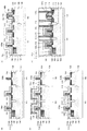
ゲート電極108bの形成後、図2(a)に示すように、ゲート電極108bをマスクとし、ゲート電極108bに近接した部分に、周辺回路領域102のトランジスタのソース・ドレイン領域を構成するn型の半導体領域114を形成する。半導体領域114は、例えばイオン注入法によって不純物を注入することによって形成される。図2(a)に示す構成では、n型のトランジスタのみを示すが、例えば、半導体層100にn型のウェルが形成され、p型の半導体領域で構成されるソース・ドレイン領域を有するp型のトランジスタも、周辺回路領域102に形成されうる。
After the formation of the
次に、図2(b)に示すように、画素領域101及び周辺回路領域102を覆うように、半導体層100の上に、後の工程でゲート電極108bのサイドウォールとなる絶縁膜115を成膜する。本実施形態において、絶縁膜115には、例えばTEOSを含む材料を用いて減圧CVD法によって形成された酸化シリコン膜を用いる。絶縁膜115を形成する際、半導体領域114に注入された不純物の拡散を抑制するために、TEOSを含む材料を用いて減圧CVD法によって形成する酸化シリコン膜112aよりも低温で成膜してもよい。
Next, as illustrated in FIG. 2B, an insulating
絶縁膜115の形成後、画素領域101の上に配された絶縁膜115を覆うマスクパターン122dを形成し、周辺回路領域102の上に配された絶縁膜115をドライエッチングによってエッチバックする。このエッチバックの工程によって、図2(c)に示すように画素領域101の絶縁膜112の上に絶縁膜115の一部を残した状態で、絶縁膜115からゲート電極108bの側壁を覆うサイドウォール116が形成される。絶縁膜115のうち画素領域101の上に配された部分を残すことによって、後の工程で周辺回路領域102の半導体領域114やゲート電極108bの表面に金属シリサイドを形成する際のシリサイドプロテクション膜として絶縁膜115を用いることができる。サイドウォール116の形成後、絶縁膜115が、画素領域101の全体を覆っていてもよい。
After the formation of the insulating
図2(c)に示す構成のように、絶縁膜112は、サイドウォール116を構成する酸化シリコンとは異なる絶縁体である窒化シリコン膜112bを含む。ここで、絶縁膜112の水素濃度が、サイドウォール116の水素濃度よりも高くてもよい。サイドウォール116を形成するための絶縁膜115に用いられる酸化シリコン膜は、絶縁膜112を構成する窒化シリコン膜112bと比較して、膜中に含まれる水素の濃度が低くなりうる。また、絶縁膜115を成膜する際に、絶縁膜115が絶縁膜112よりも水素濃度が低くなるような条件を適宜選択し、絶縁膜115を形成してもよい。ここで、絶縁膜112及びサイドウォール116の水素濃度とは、例えば絶縁膜112、及び、サイドウォール116それぞれのある領域中の平均の水素濃度であってもよい。また例えば、絶縁膜112、及び、サイドウォール116それぞれのうち最も高い水素濃度であってもよい。水素濃度は、例えば飛行時間型の二次イオン質量分析法などを用いて測定することができる。
As illustrated in FIG. 2C, the insulating
画素領域101でダングリングボンドを終端するために必要とされる水素の量は、画素領域101に配されたトランジスタよりも微細化された周辺回路領域102に配されたトランジスタに必要とされる水素の量に対して過剰な場合がある。トランジスタに過剰な水素が供給されると、トランジスタのNBTI特性やホットキャリアによる特性などが悪化する可能性がある。このため本実施形態では、ゲート電極108bのサイドウォールとなる絶縁膜115に、画素領域101への水素供給膜として機能する窒化シリコン膜112bを含む絶縁膜112よりも水素濃度が低い絶縁膜が用いられる。
The amount of hydrogen required to terminate the dangling bond in the
また、サイドウォール116を形成する際に、画素領域101の上に配された絶縁膜115は、本実施形態のように画素領域101上に残存せずに、例えばエッチングされてもよい。例えば、絶縁膜115からサイドウォール116を形成する際、マスクパターン122dを形成せずに、画素領域101及び周辺回路領域102の全面をドライエッチングによってエッチバックしてもよい。マスクパターン122dを形成しないことによって、固体撮像装置の製造コストを低減できる。この場合、サイドウォール116の形成後、画素領域101上に配された絶縁膜112の少なくとも一部が残ることによって、画素領域101の半導体層100に対するダメージを抑制することができる。
Further, when forming the
サイドウォール116の形成後、周辺回路領域102のトランジスタのLDD構造のソース・ドレイン領域を構成するn型の半導体領域117をイオン注入法によって不純物を注入し形成する。ソース・ドレイン領域がLDD構造を有さない場合、半導体領域114を形成する際の不純物の注入量を適宜、調整し、半導体領域117を形成しなくてもよい。次いで、画素領域101及び周辺回路領域102を覆うように半導体層100の上にコバルトやニッケルなどの金属を形成する。形成された金属を周辺回路領域102のゲート電極108bや半導体領域114、117と反応させることによって、ゲート電極108b及び半導体領域114、117によって構成されるソース・ドレイン領域の表面に金属シリサイド118が形成される。
After the formation of the
金属シリサイド118を形成後、周辺回路領域102のエッチストッパとして機能する窒化シリコン膜119を画素領域101及び周辺回路領域102を覆うように半導体層100上に形成する。窒化シリコン膜119は、窒化シリコン膜112bと異なる成膜条件を用いることによって、膜中に含まれる水素濃度を窒化シリコン膜112bよりも低くなるように形成してもよい。次いで、周辺回路領域102を覆うマスクパターンを形成し、画素領域101の上に配された窒化シリコン膜119を等方性ドライエッチングによって除去する。画素領域101の上に配された窒化シリコン膜119をエッチングした際の断面図を図2(d)に示す。窒化シリコン膜119は、周辺回路領域102のトランジスタのストレスライナ膜として機能するような成膜条件で形成されてもよい。図2(d)に示す構成では、画素領域101の窒化シリコン膜119をすべて除去しているが、これに限られるわけではない。例えば、光電変換部の上に光導波路を形成する場合、絶縁膜112上に形成される層間絶縁膜に光導波路を配するための開口部を形成する際のエッチングストッパ膜として機能するように、該当する部分に窒化シリコン膜119を残してもよい。
After the
次いで、層間絶縁膜120を形成する。層間絶縁膜120には、例えば高密度プラズマCVD法によって成膜されたBPSGやBSG、PSGなどの酸化シリコンを用いてもよい。層間絶縁膜120の形成後、画素領域101において、絶縁膜112をエッチングストップ膜として用い、半導体領域110、111やゲート電極108aと電気的な接続をするためのコンタクトホールを開口する。コンタクトホールの開口には、例えば異方性のドライエッチングを用いてもよい。半導体領域110、111に形成されるコンタクトホールは、絶縁膜112がサイドウォールとして機能することによって自己整合的に半導体領域110、111の上に形成されうる。コンタクトホールの開口後、コンタクトホールに形成されるコンタクトプラグと半導体領域110、111との間の電気的な接続がより確実となるように、コンタクトホールの開口部を通してイオン注入法によって不純物を注入してもよい。次に、周辺回路領域102においても、窒化シリコン膜119をエッチングストップ膜として用い、周辺回路領域102のトランジスタのゲート電極108bやソース・ドレイン領域と電気的に接続するためのコンタクトホールを開口する。画素領域101のコンタクトホールの開口と同様に、ドライエッチングを用いてコンタクトホールを形成してもよい。画素領域101と周辺回路領域102とで、コンタクトホールを形成する順番は、本実施形態に限らず、周辺回路領域102の方が先であってもよいし、画素領域101と周辺回路領域102とで同時にコンタクトホールを形成してもよい。続いてコンタクトホールの中に導電体を充填して電極121a、121bを形成する。電極121a、121bの形成された断面図を図2(e)に示す。その後、金属など用いた配線や、カラーフィルタ、マイクロレンズなどを形成し、固体撮像装置が完成する。また、配線を形成する工程の最終工程で画素領域101及び周辺回路領域102に配されたトランジスタへの水素供給を促進させるための水素アニール工程を追加してもよい。
Next, an
以上、説明したように、ポリシリコン膜107から、画素領域101と周辺回路領域102とで、それぞれ別の工程でゲート電極108a及びゲート電極108bを形成する。また、画素領域101のゲート電極108aや他の構成要素を形成する際は、周辺回路領域102がポリシリコン膜107で覆われ、周辺回路領域102のゲート電極108bや他の構成要素を形成する際は、画素領域101が絶縁膜112で覆われる。このような工程を用いることによって、固体撮像装置を製造する際のエッチング処理の際の画素領域101及び周辺回路領域102の半導体層100へのダメージを抑制することが可能となる。結果として、画素領域101の光電変換部で発生するノイズを低減できる。また、画素領域101及び周辺回路領域102にそれぞれ配されたトランジスタの特性のばらつきを抑制することができる。更に、画素領域101を覆う絶縁膜112と周辺回路領域102のサイドウォール116を構成する絶縁膜115とで、それぞれ異なる構成を有する絶縁体を形成する。絶縁膜112が、絶縁膜115から形成されるサイドウォール116の水素濃度よりも高い水素濃度を有することによって、画素領域101ではダングリングボンドを効果的に終端しノイズを低減する。また、周辺回路領域102への過剰な水素の供給を抑制することによって、周辺回路領域102に配されたトランジスタの特性の低下を抑制することができる。
As described above, the
以上、本発明に係る実施形態を示したが、本発明はこれらの実施形態に限定されないことはいうまでもなく、本発明の要旨を逸脱しない範囲で、上述した実施形態は適宜変更、組み合わせが可能である。 As mentioned above, although embodiment which concerns on this invention was shown, it cannot be overemphasized that this invention is not limited to these embodiment, In the range which does not deviate from the summary of this invention, embodiment mentioned above can be changed and combined suitably. Is possible.
100:半導体層、101:画素領域、102:周辺回路領域、108a、b:ゲート電極、112、115:絶縁膜、122a、b、c、d:マスクパターン 100: Semiconductor layer, 101: Pixel region, 102: Peripheral circuit region, 108a, b: Gate electrode, 112, 115: Insulating film, 122a, b, c, d: Mask pattern
Claims (11)
前記半導体層の上にゲート電極膜を成膜する工程と、
前記ゲート電極膜をエッチングし、前記周辺回路領域に前記ゲート電極膜を残存させるとともに、前記画素領域にパターニングされた第1のゲート電極を形成する工程と、
前記第1のゲート電極を形成する工程の後に、前記半導体層の上に第1の絶縁膜を成膜する工程と、
前記周辺回路領域に形成された前記第1の絶縁膜を除去する工程と、
前記第1の絶縁膜を除去する工程の後に、前記周辺回路領域に残存していた前記ゲート電極膜をエッチングし、前記周辺回路領域にパターニングされた第2のゲート電極を形成する工程と、
を含むことを特徴とする固体撮像装置の製造方法。 A manufacturing method of a solid-state imaging device in which a pixel region and a peripheral circuit region are arranged in a semiconductor layer,
Forming a gate electrode film on the semiconductor layer;
Etching the gate electrode film, leaving the gate electrode film in the peripheral circuit region, and forming a patterned first gate electrode in the pixel region;
After the step of forming the first gate electrode, forming a first insulating film on the semiconductor layer;
Removing the first insulating film formed in the peripheral circuit region;
Etching the gate electrode film remaining in the peripheral circuit region after the step of removing the first insulating film, and forming a second gate electrode patterned in the peripheral circuit region;
A method for manufacturing a solid-state imaging device, comprising:
前記第2の絶縁膜をエッチングすることによって、前記第2のゲート電極の側壁にサイドウォールを形成する工程と、
を更に含むことを特徴とする請求項1に記載の固体撮像装置の製造方法。 After the step of forming the second gate electrode, forming a second insulating film on the semiconductor layer;
Etching the second insulating film to form a sidewall on the side wall of the second gate electrode;
The method for manufacturing a solid-state imaging device according to claim 1, further comprising:
前記第1の絶縁膜をエッチングする工程が、前記窒化シリコン膜を等方性ドライエッチングする工程と、前記窒化シリコン膜をエッチングした後に前記酸化シリコン膜をウエットエッチングする工程と、を含むことを特徴とする請求項7に記載の固体撮像装置の製造方法。 The first insulating film is laminated in the order of the silicon oxide film and the silicon nitride film from the semiconductor layer side,
The step of etching the first insulating film includes a step of isotropic dry etching the silicon nitride film, and a step of wet etching the silicon oxide film after etching the silicon nitride film. A method for manufacturing a solid-state imaging device according to claim 7.
前記第2のゲート電極を形成する工程の後、前記半導体層のうち前記第2のゲート電極に近接した部分にソース・ドレイン領域を形成する工程と、
前記第2のゲート電極及び前記ソース・ドレイン領域の表面に金属シリサイドを形成する工程と、を更に含むことを特徴とする請求項1乃至10の何れか1項に記載の固体撮像装置の製造方法。 The manufacturing method includes:
After the step of forming the second gate electrode, forming a source / drain region in a portion of the semiconductor layer adjacent to the second gate electrode;
The method of manufacturing a solid-state imaging device according to claim 1, further comprising: forming a metal silicide on surfaces of the second gate electrode and the source / drain regions. .
Priority Applications (2)
| Application Number | Priority Date | Filing Date | Title |
|---|---|---|---|
| JP2016073178A JP2017183668A (en) | 2016-03-31 | 2016-03-31 | Manufacturing method for solid-state image pickup device |
| US15/455,343 US9917135B2 (en) | 2016-03-31 | 2017-03-10 | Method of manufacturing solid-state image sensor |
Applications Claiming Priority (1)
| Application Number | Priority Date | Filing Date | Title |
|---|---|---|---|
| JP2016073178A JP2017183668A (en) | 2016-03-31 | 2016-03-31 | Manufacturing method for solid-state image pickup device |
Publications (2)
| Publication Number | Publication Date |
|---|---|
| JP2017183668A true JP2017183668A (en) | 2017-10-05 |
| JP2017183668A5 JP2017183668A5 (en) | 2019-05-09 |
Family
ID=59961227
Family Applications (1)
| Application Number | Title | Priority Date | Filing Date |
|---|---|---|---|
| JP2016073178A Pending JP2017183668A (en) | 2016-03-31 | 2016-03-31 | Manufacturing method for solid-state image pickup device |
Country Status (2)
| Country | Link |
|---|---|
| US (1) | US9917135B2 (en) |
| JP (1) | JP2017183668A (en) |
Cited By (1)
| Publication number | Priority date | Publication date | Assignee | Title |
|---|---|---|---|---|
| JP2019067826A (en) * | 2017-09-28 | 2019-04-25 | キヤノン株式会社 | Imaging apparatus, method of manufacturing the same, and apparatus |
Families Citing this family (1)
| Publication number | Priority date | Publication date | Assignee | Title |
|---|---|---|---|---|
| JP2019029448A (en) | 2017-07-27 | 2019-02-21 | キヤノン株式会社 | Imaging device, camera, and manufacturing method of imaging device |
Citations (3)
| Publication number | Priority date | Publication date | Assignee | Title |
|---|---|---|---|---|
| JP2007324306A (en) * | 2006-05-31 | 2007-12-13 | Fujifilm Corp | Method of manufacturing solid-state imaging device |
| JP2008252032A (en) * | 2007-03-30 | 2008-10-16 | Sony Corp | Solid-state imaging element and method for manufacturing the same |
| JP2013084693A (en) * | 2011-10-06 | 2013-05-09 | Canon Inc | Solid state image pickup device and manufacturing method of the same, and camera |
Family Cites Families (3)
| Publication number | Priority date | Publication date | Assignee | Title |
|---|---|---|---|---|
| KR100745596B1 (en) * | 2004-11-29 | 2007-08-02 | 삼성전자주식회사 | Image sensor and method for forming the same |
| JP2015216176A (en) * | 2014-05-08 | 2015-12-03 | キヤノン株式会社 | Method of manufacturing semiconductor device, and semiconductor device |
| JP2016001709A (en) * | 2014-06-12 | 2016-01-07 | キヤノン株式会社 | Solid state image pickup device manufacturing method |
-
2016
- 2016-03-31 JP JP2016073178A patent/JP2017183668A/en active Pending
-
2017
- 2017-03-10 US US15/455,343 patent/US9917135B2/en active Active
Patent Citations (3)
| Publication number | Priority date | Publication date | Assignee | Title |
|---|---|---|---|---|
| JP2007324306A (en) * | 2006-05-31 | 2007-12-13 | Fujifilm Corp | Method of manufacturing solid-state imaging device |
| JP2008252032A (en) * | 2007-03-30 | 2008-10-16 | Sony Corp | Solid-state imaging element and method for manufacturing the same |
| JP2013084693A (en) * | 2011-10-06 | 2013-05-09 | Canon Inc | Solid state image pickup device and manufacturing method of the same, and camera |
Cited By (2)
| Publication number | Priority date | Publication date | Assignee | Title |
|---|---|---|---|---|
| JP2019067826A (en) * | 2017-09-28 | 2019-04-25 | キヤノン株式会社 | Imaging apparatus, method of manufacturing the same, and apparatus |
| JP7076971B2 (en) | 2017-09-28 | 2022-05-30 | キヤノン株式会社 | Imaging equipment and its manufacturing method and equipment |
Also Published As
| Publication number | Publication date |
|---|---|
| US20170287974A1 (en) | 2017-10-05 |
| US9917135B2 (en) | 2018-03-13 |
Similar Documents
| Publication | Publication Date | Title |
|---|---|---|
| KR100761829B1 (en) | semiconductor device, CMOS image sensor, method for manufacturing the semiconductor device and method for manufacturing the CMOS image sensor | |
| US10784303B2 (en) | Method of manufacturing a CMOS image sensor | |
| KR100801053B1 (en) | Method of isolating a device and method of forming an image device using the same | |
| JP2011129935A (en) | Method of manufacturing cmos image sensor | |
| KR20000060693A (en) | Semiconductor device and method for fabricating the same | |
| KR20080062064A (en) | Cmos image sensor and method of manufaturing thereof | |
| US7928483B2 (en) | Semiconductor device and method for manufacturing same | |
| US7989252B2 (en) | Method for fabricating pixel cell of CMOS image sensor | |
| US20080210995A1 (en) | Image sensor and method for fabricating the same | |
| JP2013089652A (en) | Solid state image sensor and manufacturing method therefor | |
| US20120205777A1 (en) | Semiconductor device and method for fabricating the same | |
| US9842871B2 (en) | Method of manufacturing semiconductor device | |
| JP7418383B2 (en) | Imaging device and camera | |
| KR20040061967A (en) | Method for forming isolation layer of semiconductor device | |
| US9917135B2 (en) | Method of manufacturing solid-state image sensor | |
| KR20100138087A (en) | Image sensor and method for manufacuring thereof | |
| JP2017117855A (en) | Method of manufacturing imaging device | |
| US20070023841A1 (en) | Transistor and method for forming the same | |
| KR20070059234A (en) | Apparatus for manufacturing a image sensor for reducing a dark current | |
| JP2009176950A (en) | Solid-state image sensor and method of manufacturing the same process | |
| US6982187B2 (en) | Methods of making shallow trench-type pixels for CMOS image sensors | |
| US8178937B2 (en) | Image sensor and method for manufacturing the same | |
| KR100605908B1 (en) | Semiconductor Device And Method For Manufacturing The Same | |
| JP2010067683A (en) | Semiconductor device and its manufacturing method | |
| KR20070064856A (en) | Method for manufacturing image sensor |
Legal Events
| Date | Code | Title | Description |
|---|---|---|---|
| A521 | Request for written amendment filed |
Free format text: JAPANESE INTERMEDIATE CODE: A523 Effective date: 20190319 |
|
| A621 | Written request for application examination |
Free format text: JAPANESE INTERMEDIATE CODE: A621 Effective date: 20190319 |
|
| A977 | Report on retrieval |
Free format text: JAPANESE INTERMEDIATE CODE: A971007 Effective date: 20200116 |
|
| A131 | Notification of reasons for refusal |
Free format text: JAPANESE INTERMEDIATE CODE: A131 Effective date: 20200225 |
|
| A601 | Written request for extension of time |
Free format text: JAPANESE INTERMEDIATE CODE: A601 Effective date: 20200403 |
|
| A521 | Request for written amendment filed |
Free format text: JAPANESE INTERMEDIATE CODE: A523 Effective date: 20200623 |
|
| A02 | Decision of refusal |
Free format text: JAPANESE INTERMEDIATE CODE: A02 Effective date: 20201130 |
|
| RD01 | Notification of change of attorney |
Free format text: JAPANESE INTERMEDIATE CODE: A7421 Effective date: 20210103 |
|
| A521 | Request for written amendment filed |
Free format text: JAPANESE INTERMEDIATE CODE: A523 Effective date: 20210113 |