JP2017175746A - Current detection circuit and dc-dc converter comprising the same - Google Patents
Current detection circuit and dc-dc converter comprising the same Download PDFInfo
- Publication number
- JP2017175746A JP2017175746A JP2016057925A JP2016057925A JP2017175746A JP 2017175746 A JP2017175746 A JP 2017175746A JP 2016057925 A JP2016057925 A JP 2016057925A JP 2016057925 A JP2016057925 A JP 2016057925A JP 2017175746 A JP2017175746 A JP 2017175746A
- Authority
- JP
- Japan
- Prior art keywords
- transistor
- voltage
- terminal
- current
- detection circuit
- Prior art date
- Legal status (The legal status is an assumption and is not a legal conclusion. Google has not performed a legal analysis and makes no representation as to the accuracy of the status listed.)
- Granted
Links
Images


Classifications
-
- G—PHYSICS
- G01—MEASURING; TESTING
- G01R—MEASURING ELECTRIC VARIABLES; MEASURING MAGNETIC VARIABLES
- G01R19/00—Arrangements for measuring currents or voltages or for indicating presence or sign thereof
- G01R19/0092—Arrangements for measuring currents or voltages or for indicating presence or sign thereof measuring current only
-
- G—PHYSICS
- G01—MEASURING; TESTING
- G01R—MEASURING ELECTRIC VARIABLES; MEASURING MAGNETIC VARIABLES
- G01R15/00—Details of measuring arrangements of the types provided for in groups G01R17/00 - G01R29/00, G01R33/00 - G01R33/26 or G01R35/00
- G01R15/14—Adaptations providing voltage or current isolation, e.g. for high-voltage or high-current networks
- G01R15/146—Measuring arrangements for current not covered by other subgroups of G01R15/14, e.g. using current dividers, shunts, or measuring a voltage drop
-
- G—PHYSICS
- G01—MEASURING; TESTING
- G01R—MEASURING ELECTRIC VARIABLES; MEASURING MAGNETIC VARIABLES
- G01R31/00—Arrangements for testing electric properties; Arrangements for locating electric faults; Arrangements for electrical testing characterised by what is being tested not provided for elsewhere
- G01R31/40—Testing power supplies
-
- H—ELECTRICITY
- H02—GENERATION; CONVERSION OR DISTRIBUTION OF ELECTRIC POWER
- H02M—APPARATUS FOR CONVERSION BETWEEN AC AND AC, BETWEEN AC AND DC, OR BETWEEN DC AND DC, AND FOR USE WITH MAINS OR SIMILAR POWER SUPPLY SYSTEMS; CONVERSION OF DC OR AC INPUT POWER INTO SURGE OUTPUT POWER; CONTROL OR REGULATION THEREOF
- H02M1/00—Details of apparatus for conversion
- H02M1/08—Circuits specially adapted for the generation of control voltages for semiconductor devices incorporated in static converters
-
- H—ELECTRICITY
- H02—GENERATION; CONVERSION OR DISTRIBUTION OF ELECTRIC POWER
- H02M—APPARATUS FOR CONVERSION BETWEEN AC AND AC, BETWEEN AC AND DC, OR BETWEEN DC AND DC, AND FOR USE WITH MAINS OR SIMILAR POWER SUPPLY SYSTEMS; CONVERSION OF DC OR AC INPUT POWER INTO SURGE OUTPUT POWER; CONTROL OR REGULATION THEREOF
- H02M1/00—Details of apparatus for conversion
- H02M1/14—Arrangements for reducing ripples from dc input or output
- H02M1/15—Arrangements for reducing ripples from dc input or output using active elements
-
- H—ELECTRICITY
- H02—GENERATION; CONVERSION OR DISTRIBUTION OF ELECTRIC POWER
- H02M—APPARATUS FOR CONVERSION BETWEEN AC AND AC, BETWEEN AC AND DC, OR BETWEEN DC AND DC, AND FOR USE WITH MAINS OR SIMILAR POWER SUPPLY SYSTEMS; CONVERSION OF DC OR AC INPUT POWER INTO SURGE OUTPUT POWER; CONTROL OR REGULATION THEREOF
- H02M3/00—Conversion of dc power input into dc power output
- H02M3/02—Conversion of dc power input into dc power output without intermediate conversion into ac
- H02M3/04—Conversion of dc power input into dc power output without intermediate conversion into ac by static converters
- H02M3/10—Conversion of dc power input into dc power output without intermediate conversion into ac by static converters using discharge tubes with control electrode or semiconductor devices with control electrode
- H02M3/145—Conversion of dc power input into dc power output without intermediate conversion into ac by static converters using discharge tubes with control electrode or semiconductor devices with control electrode using devices of a triode or transistor type requiring continuous application of a control signal
- H02M3/155—Conversion of dc power input into dc power output without intermediate conversion into ac by static converters using discharge tubes with control electrode or semiconductor devices with control electrode using devices of a triode or transistor type requiring continuous application of a control signal using semiconductor devices only
- H02M3/156—Conversion of dc power input into dc power output without intermediate conversion into ac by static converters using discharge tubes with control electrode or semiconductor devices with control electrode using devices of a triode or transistor type requiring continuous application of a control signal using semiconductor devices only with automatic control of output voltage or current, e.g. switching regulators
- H02M3/1563—Conversion of dc power input into dc power output without intermediate conversion into ac by static converters using discharge tubes with control electrode or semiconductor devices with control electrode using devices of a triode or transistor type requiring continuous application of a control signal using semiconductor devices only with automatic control of output voltage or current, e.g. switching regulators without using an external clock
-
- H—ELECTRICITY
- H02—GENERATION; CONVERSION OR DISTRIBUTION OF ELECTRIC POWER
- H02M—APPARATUS FOR CONVERSION BETWEEN AC AND AC, BETWEEN AC AND DC, OR BETWEEN DC AND DC, AND FOR USE WITH MAINS OR SIMILAR POWER SUPPLY SYSTEMS; CONVERSION OF DC OR AC INPUT POWER INTO SURGE OUTPUT POWER; CONTROL OR REGULATION THEREOF
- H02M3/00—Conversion of dc power input into dc power output
- H02M3/02—Conversion of dc power input into dc power output without intermediate conversion into ac
- H02M3/04—Conversion of dc power input into dc power output without intermediate conversion into ac by static converters
- H02M3/10—Conversion of dc power input into dc power output without intermediate conversion into ac by static converters using discharge tubes with control electrode or semiconductor devices with control electrode
- H02M3/145—Conversion of dc power input into dc power output without intermediate conversion into ac by static converters using discharge tubes with control electrode or semiconductor devices with control electrode using devices of a triode or transistor type requiring continuous application of a control signal
- H02M3/155—Conversion of dc power input into dc power output without intermediate conversion into ac by static converters using discharge tubes with control electrode or semiconductor devices with control electrode using devices of a triode or transistor type requiring continuous application of a control signal using semiconductor devices only
- H02M3/156—Conversion of dc power input into dc power output without intermediate conversion into ac by static converters using discharge tubes with control electrode or semiconductor devices with control electrode using devices of a triode or transistor type requiring continuous application of a control signal using semiconductor devices only with automatic control of output voltage or current, e.g. switching regulators
- H02M3/158—Conversion of dc power input into dc power output without intermediate conversion into ac by static converters using discharge tubes with control electrode or semiconductor devices with control electrode using devices of a triode or transistor type requiring continuous application of a control signal using semiconductor devices only with automatic control of output voltage or current, e.g. switching regulators including plural semiconductor devices as final control devices for a single load
-
- H—ELECTRICITY
- H02—GENERATION; CONVERSION OR DISTRIBUTION OF ELECTRIC POWER
- H02M—APPARATUS FOR CONVERSION BETWEEN AC AND AC, BETWEEN AC AND DC, OR BETWEEN DC AND DC, AND FOR USE WITH MAINS OR SIMILAR POWER SUPPLY SYSTEMS; CONVERSION OF DC OR AC INPUT POWER INTO SURGE OUTPUT POWER; CONTROL OR REGULATION THEREOF
- H02M1/00—Details of apparatus for conversion
- H02M1/0003—Details of control, feedback or regulation circuits
- H02M1/0009—Devices or circuits for detecting current in a converter
Abstract
Description
本発明は、電流検出回路及びそれを備えたDCDCコンバータに関し、例えば低コスト化が可能な電流検出回路及びそれを備えたDCDCコンバータに関する。 The present invention relates to a current detection circuit and a DCDC converter including the current detection circuit, for example, a current detection circuit capable of reducing costs and a DCDC converter including the current detection circuit.
特許文献1には、駆動回路に流れる電流を検出する電流検出回路の構成が開示されている。
具体的には、電流検出回路は、駆動回路のハイサイド側に設けられたNチャネル型のドライブトランジスタに流れる電流を検出する回路であって、ドレイン及びゲートがそれぞれドライブトランジスタのドレイン及びゲートに接続されたセンストランジスタと、センストランジスタのソース電圧とドライブトランジスタのソース電圧との電位差を増幅するオペアンプと、センストランジスタに直列接続され、ゲートにオペアンプの出力電圧が供給されるトランジスタと、を少なくとも有する。 Specifically, the current detection circuit is a circuit that detects a current flowing in an N-channel type drive transistor provided on the high side of the drive circuit, and has a drain and a gate connected to the drain and gate of the drive transistor, respectively. At least a sense transistor, an operational amplifier that amplifies the potential difference between the source voltage of the sense transistor and the source voltage of the drive transistor, and a transistor that is connected in series to the sense transistor and that is supplied with the output voltage of the operational amplifier.
ここで、センストランジスタのゲート−ソース間電圧及びドレイン−ソース間電圧は、それぞれドライブトランジスタのゲート−ソース間電圧及びドレイン−ソース間電圧と同じ値を示す。そのため、センストランジスタには、ドライブトランジスタに流れる電流に比例する電流(例えば1000分の1の電流)が流れる。この電流検出回路は、センストランジスタに流れる電流を検出することによって、駆動回路に流れる電流(より詳しくはドライブトランジスタのドレイン及びソース間に流れる電流)を精度良く検出することができる。 Here, the gate-source voltage and the drain-source voltage of the sense transistor have the same values as the gate-source voltage and the drain-source voltage of the drive transistor, respectively. Therefore, a current proportional to the current flowing through the drive transistor (for example, a current of 1/1000) flows through the sense transistor. This current detection circuit can accurately detect a current flowing through the drive circuit (more specifically, a current flowing between the drain and source of the drive transistor) by detecting the current flowing through the sense transistor.
ここで、特許文献1に開示された電流検出回路の構成では、駆動回路に設けられたドライブトランジスタのスイッチング周波数が高い場合、オペアンプの入力端子に供給される電圧が接地電圧及び入力電圧間を高速に変化することになるため、オペアンプには非常に高速な動作が求められてしまう。そのため、特許文献1に開示された電流検出回路では、高速動作に対応可能な高価なオペアンプが必要になり、その結果、製造コストが増大してしまうという問題があった。その他の課題と新規な特徴は、本明細書の記述および添付図面から明らかになるであろう。
Here, in the configuration of the current detection circuit disclosed in
一実施の形態によれば、電流検出回路は、第1端子と制御端子とが、駆動回路のハイサイド側に設けられた第1ドライブトランジスタの端子のうち、前記駆動回路の外部に出力電圧が出力される外部出力端子側に設けられた第1端子と、制御端子と、にそれぞれ接続された、前記第1ドライブトランジスタと同一導電型の第1センストランジスタと、前記第1ドライブトランジスタの端子のうち、前記駆動回路の外部から入力電圧が供給される外部入力端子側に設けられた第2端子、の電圧と、前記第1センストランジスタの第2端子の電圧と、の電位差を増幅する第1オペアンプと、前記第1センストランジスタに流れる電流が流れる第1電流経路上に設けられ、制御端子に前記第1オペアンプの出力電圧が供給される第1電流制御トランジスタと、を備え、前記第1センストランジスタに流れる電流の値から前記第1ドライブトランジスタに流れる電流の値が検出される。 According to one embodiment, the current detection circuit has a first terminal and a control terminal whose output voltage is external to the drive circuit out of the terminals of the first drive transistor provided on the high side of the drive circuit. A first sense transistor having the same conductivity type as that of the first drive transistor and a terminal of the first drive transistor, which are respectively connected to a first terminal provided on the output side of the output terminal and a control terminal; Of these, a first that amplifies a potential difference between a voltage at a second terminal provided on the side of an external input terminal to which an input voltage is supplied from the outside of the drive circuit, and a voltage at a second terminal of the first sense transistor. An operational amplifier and a first current control transistor provided on a first current path through which a current flowing through the first sense transistor flows, and an output voltage of the first operational amplifier is supplied to a control terminal. It includes static and, the value of current flowing through the first drive transistor from the value of the current flowing through the first sense transistor is detected.
また、一実施の形態によれば、電流検出回路は、ソース及びゲートが、駆動回路のハイサイド側に設けられたNチャネル型の第1ドライブトランジスタのソース及びゲートにそれぞれ接続されたNチャネル型の第1センストランジスタと、前記第1ドライブトランジスタのドレイン電圧と、前記第1センストランジスタのドレイン電圧と、の電位差を増幅する第1オペアンプと、前記第1センストランジスタに流れる電流が流れる第1電流経路上に設けられ、ゲートに前記第1オペアンプの出力電圧が供給される第1電流制御トランジスタと、を備え、前記第1センストランジスタに流れる電流の値から前記第1ドライブトランジスタに流れる電流の値が検出される。 According to one embodiment, the current detection circuit includes an N-channel type in which a source and a gate are respectively connected to a source and a gate of an N-channel type first drive transistor provided on the high side of the drive circuit. A first operational amplifier that amplifies a potential difference between the first sense transistor, the drain voltage of the first drive transistor, and the drain voltage of the first sense transistor, and a first current that flows through the first sense transistor A first current control transistor provided on a path and supplied with an output voltage of the first operational amplifier at a gate, and a value of a current flowing in the first drive transistor from a value of a current flowing in the first sense transistor Is detected.
前記一実施の形態によれば、製造コストの増大を抑制することが可能な電流検出回路及びそれを備えたDCDCコンバータを提供することができる。 According to the embodiment, it is possible to provide a current detection circuit capable of suppressing an increase in manufacturing cost and a DCDC converter including the current detection circuit.
以下、図面を参照しつつ、実施の形態について説明する。なお、図面は簡略的なものであるから、この図面の記載を根拠として実施の形態の技術的範囲を狭く解釈してはならない。また、同一の要素には、同一の符号を付し、重複する説明は省略する。 Hereinafter, embodiments will be described with reference to the drawings. Since the drawings are simple, the technical scope of the embodiments should not be narrowly interpreted based on the description of the drawings. Moreover, the same code | symbol is attached | subjected to the same element and the overlapping description is abbreviate | omitted.
以下の実施の形態においては便宜上その必要があるときは、複数のセクションまたは実施の形態に分割して説明するが、特に明示した場合を除き、それらはお互いに無関係なものではなく、一方は他方の一部または全部の変形例、応用例、詳細説明、補足説明等の関係にある。また、以下の実施の形態において、要素の数等(個数、数値、量、範囲等を含む)に言及する場合、特に明示した場合および原理的に明らかに特定の数に限定される場合等を除き、その特定の数に限定されるものではなく、特定の数以上でも以下でもよい。 In the following embodiments, when it is necessary for the sake of convenience, the description will be divided into a plurality of sections or embodiments. However, unless otherwise specified, they are not irrelevant to each other. Are partly or entirely modified, application examples, detailed explanations, supplementary explanations, and the like. Further, in the following embodiments, when referring to the number of elements (including the number, numerical value, quantity, range, etc.), especially when clearly indicated and when clearly limited to a specific number in principle, etc. Except, it is not limited to the specific number, and may be more or less than the specific number.
さらに、以下の実施の形態において、その構成要素(動作ステップ等も含む)は、特に明示した場合および原理的に明らかに必須であると考えられる場合等を除き、必ずしも必須のものではない。同様に、以下の実施の形態において、構成要素等の形状、位置関係等に言及するときは、特に明示した場合および原理的に明らかにそうでないと考えられる場合等を除き、実質的にその形状等に近似または類似するもの等を含むものとする。このことは、上記数等(個数、数値、量、範囲等を含む)についても同様である。 Further, in the following embodiments, the constituent elements (including operation steps and the like) are not necessarily essential except when clearly indicated and clearly considered essential in principle. Similarly, in the following embodiments, when referring to the shapes, positional relationships, etc. of the components, etc., the shapes are substantially the same unless otherwise specified, or otherwise apparent in principle. And the like are included. The same applies to the above numbers and the like (including the number, numerical value, quantity, range, etc.).
<実施の形態1>
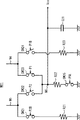
図1は、実施の形態1にかかる電流検出回路10を示すブロック図である。本実施の形態にかかる電流検出回路10は、駆動回路のハイサイド側に設けられたNチャネル型のドライブトランジスタのドレイン−ソース間に流れる電流を検出する回路である。以下、具体的に説明する。
<
FIG. 1 is a block diagram of a
図1に示すように、電流検出回路10は、トランジスタMN1〜MN3,MP1〜MP4と、オペアンプ(第1オペアンプ)A1と、抵抗素子R1と、レギュレータRG1と、を備える。なお、図1には、駆動回路12に設けられた構成要素の一部であるトランジスタTr1、トランジスタTr2及びインダクタL1も示されている。
As shown in FIG. 1, the
駆動回路12は、入力電圧Vinを駆動して出力電圧Voutを出力する回路であって、例えばピーク電流モード制御方式が採用された降圧型のDCDCコンバータの出力段に設けられる。
The
駆動回路12において、トランジスタTr1は、駆動回路12のハイサイド側に設けられたドライブトランジスタ(第1ドライブトランジスタ)であって、高耐圧のNチャネルMOSトランジスタにより構成されている。トランジスタTr2は、駆動回路12のローサイド側に設けられたドライブトランジスタ(第2ドライブトランジスタ)であって、高耐圧のNチャネルMOSトランジスタにより構成されている。
In the
より詳細には、トランジスタTr1では、ドレイン(第2端子)が入力端子INに接続され、ソース(第1端子)がインダクタL1の一端(ノードN1)に接続され、ゲート(制御端子)に制御部(不図示)からのパルス信号P1が供給される。トランジスタTr2では、ドレイン(第2端子)がノードN1に接続され、ソース(第1端子)が接地電圧端子GNDに接続され、ゲート(制御端子)に制御部(不図示)からのパルス信号P2が供給される。なお、入力端子INには、外部から入力電圧Vinが供給され、接地電圧端子GNDには、接地電圧GNDが供給されている。また、インダクタの他端(ノードN2)は、出力端子OUTに接続される。出力端子OUTから、外部(負荷)に向けて出力電圧Voutが出力される。 More specifically, in the transistor Tr1, the drain (second terminal) is connected to the input terminal IN, the source (first terminal) is connected to one end (node N1) of the inductor L1, and the control unit is connected to the gate (control terminal). A pulse signal P1 from (not shown) is supplied. In the transistor Tr2, the drain (second terminal) is connected to the node N1, the source (first terminal) is connected to the ground voltage terminal GND, and a pulse signal P2 from a control unit (not shown) is supplied to the gate (control terminal). Supplied. The input voltage IN is supplied from the outside to the input terminal IN, and the ground voltage GND is supplied to the ground voltage terminal GND. The other end (node N2) of the inductor is connected to the output terminal OUT. An output voltage Vout is output from the output terminal OUT to the outside (load).
駆動回路12では、トランジスタTr1,Tr2のオンオフがデッドタイムを挟んで相補的に制御される。例えば、まず、トランジスタTr1がオンし、トランジスタTr2がオフすることにより、入力端子INからトランジスタTr1及びインダクタL1を介して出力端子OUTに向けて電流が流れる。このとき、インダクタL1には、電流エネルギーが蓄えられる。その後、トランジスタTr1がオフし、トランジスタTr2がオンすることにより、入力端子INからトランジスタTr1を介してインダクタL1に向けて流れていた電流が遮断される。インダクタL1は、直前に流れていた電流の電流値を維持しようとして、蓄えた電流エネルギーを出力端子OUTに向けて放出する。それにより、接地電圧端子GNDからトランジスタTr2を介して出力端子OUTに向けて電流が流れる。このような動作を繰り返すことで、駆動回路12は、入力電圧Vinをパルス信号のデューティ比に応じたレベル分だけ降圧した出力電圧Voutを出力する。
In the
電流検出回路10において、トランジスタ(第1センストランジスタ)MN1は、トランジスタTr1と同じく高耐圧のNチャネルMOSトランジスタにより構成される。例えばトランジスタMN1のトランジスタサイズはトランジスタTr1のトランジスタサイズの1/1000倍である。
In the
トランジスタMN1は、入力電圧Vinよりも高い電圧VinXが供給される高電圧端子INXと、トランジスタTr1のソース(ノードN1)と、の間の電流経路(第1電流経路)上に設けられ、ゲートにパルス信号P1が供給される。 The transistor MN1 is provided on the current path (first current path) between the high voltage terminal INX to which the voltage VinX higher than the input voltage Vin is supplied and the source of the transistor Tr1 (node N1), and has a gate A pulse signal P1 is supplied.
オペアンプA1は、入力電圧Vinが低電位側電源電圧として供給され、入力電圧Vinより高い電圧(第1電圧)Vhighが高電位側電源電圧として供給されることにより動作し、トランジスタTr1のドレイン電圧(即ち、入力電圧Vin)とトランジスタMN1のドレイン電圧との電位差を増幅する。 The operational amplifier A1 operates when the input voltage Vin is supplied as the low-potential side power supply voltage, and the voltage (first voltage) Vhigh higher than the input voltage Vin is supplied as the high-potential side power supply voltage. That is, the potential difference between the input voltage Vin) and the drain voltage of the transistor MN1 is amplified.
ここで、オペアンプA1は、トランジスタTr1のソース電圧とトランジスタMN1のソース電圧との電位差を増幅するのではなく、トランジスタTr1のドレイン電圧とトランジスタMN1のドレイン電圧との電位差を増幅している。それにより、トランジスタTr1のオンオフが高速に切り替わっている場合でも、オペアンプA1の入力端子に供給される電圧は高速に変化しないため、オペアンプA1に高速な動作が求められることはない。それにより、電流検出回路10は、高速動作に対応可能な高価なオペアンプを用いなくて良いため、製造コストの増大を抑制することができる。
Here, the operational amplifier A1 does not amplify the potential difference between the source voltage of the transistor Tr1 and the source voltage of the transistor MN1, but amplifies the potential difference between the drain voltage of the transistor Tr1 and the drain voltage of the transistor MN1. As a result, even when the transistor Tr1 is switched on and off at high speed, the voltage supplied to the input terminal of the operational amplifier A1 does not change at high speed, so that the operational amplifier A1 is not required to operate at high speed. As a result, the
また、オペアンプA1に供給される高電位側電源電圧(電圧Vhigh)及び低電位側電源電圧(入力電圧Vin)の電位差がオペアンプA1を構成する各トランジスタの耐圧以下となるように調整される。具体的には、レギュレータRG1によって生成される電圧Vhighの値を制御することによって調整される。そのため、オペアンプA1は、高耐圧のトランジスタにより構成される場合に限られず、低耐圧のトランジスタにより構成されることも可能である。それにより、オペアンプA1の精度や動作速度を向上させることができる。 Further, the potential difference between the high-potential-side power supply voltage (voltage Vhigh) and the low-potential-side power supply voltage (input voltage Vin) supplied to the operational amplifier A1 is adjusted to be equal to or lower than the withstand voltage of each transistor constituting the operational amplifier A1. Specifically, it is adjusted by controlling the value of the voltage Vhigh generated by the regulator RG1. Therefore, the operational amplifier A1 is not limited to the case of being configured with a high breakdown voltage transistor, and may be configured with a low breakdown voltage transistor. Thereby, the accuracy and operating speed of the operational amplifier A1 can be improved.
オペアンプA1の出力電圧は、トランジスタ(第1電流制御トランジスタ)MN2のゲートに供給される。トランジスタMN2は、低耐圧のNチャネルMOSトランジスタにより構成され、高電圧端子INXとノードN1との間の電流経路上においてトランジスタMN1に直列に設けられている。それにより、トランジスタTr1のドレイン電圧がトランジスタMN1のドレイン電圧にミラーされる。 The output voltage of the operational amplifier A1 is supplied to the gate of the transistor (first current control transistor) MN2. The transistor MN2 is formed of a low breakdown voltage N-channel MOS transistor, and is provided in series with the transistor MN1 on the current path between the high voltage terminal INX and the node N1. Thereby, the drain voltage of the transistor Tr1 is mirrored to the drain voltage of the transistor MN1.
ここで、トランジスタMN1のゲート−ソース間電圧及びドレイン−ソース間電圧がそれぞれトランジスタTr1のゲート−ソース間電圧及びドレイン−ソース間電圧と同じ値を示す。そのため、トランジスタMN1のドレイン−ソース間には、トランジスタTr1のドレイン−ソース間に流れる電流に比例した電流(本例では1/1000倍の電流)が精度良く流れる。 Here, the gate-source voltage and the drain-source voltage of the transistor MN1 have the same values as the gate-source voltage and the drain-source voltage of the transistor Tr1, respectively. Therefore, a current proportional to the current flowing between the drain and the source of the transistor Tr1 (1/1000 times the current in this example) flows between the drain and the source of the transistor MN1 with high accuracy.
トランジスタMN3は、高耐圧のNチャネルMOSトランジスタにより構成され、トランジスタMN2に直列に設けられている。また、トランジスタMN3のゲートにはレギュレータRG1からの電圧Vhighが供給される。なお、トランジスタMN3は、トランジスタMN2に耐圧を超える電圧が印加されるのを防ぐために設けられている。したがって、トランジスタMN2が高耐圧のトランジスタにより構成されている場合には、トランジスタMN3は設けられていなくてもよい。 The transistor MN3 is composed of a high breakdown voltage N-channel MOS transistor, and is provided in series with the transistor MN2. Further, the voltage Vhigh from the regulator RG1 is supplied to the gate of the transistor MN3. The transistor MN3 is provided to prevent a voltage exceeding the withstand voltage from being applied to the transistor MN2. Therefore, when the transistor MN2 is formed of a high breakdown voltage transistor, the transistor MN3 may not be provided.
トランジスタMP2は、低耐圧のPチャネルMOSトランジスタにより構成され、トランジスタMN1〜MN3に直列に設けられている。トランジスタMP4は、低耐圧のPチャネルMOSトランジスタにより構成され、トランジスタMP2とは別の電流経路である高電圧端子INXと接地電圧端子GNDとの間の電流経路上に設けられている。また、トランジスタMP4のゲートは、トランジスタMP2のドレイン及びゲートに接続されている。したがって、トランジスタMP4のドレイン−ソース間には、トランジスタMP2のドレイン−ソース間に流れる電流に比例する電流が流れる。つまり、トランジスタMP2,MP4はカレントミラー回路を構成している。 The transistor MP2 is formed of a low breakdown voltage P-channel MOS transistor, and is provided in series with the transistors MN1 to MN3. The transistor MP4 is formed of a low breakdown voltage P-channel MOS transistor, and is provided on a current path between the high voltage terminal INX and the ground voltage terminal GND, which is a current path different from the transistor MP2. The gate of the transistor MP4 is connected to the drain and gate of the transistor MP2. Therefore, a current proportional to the current flowing between the drain and source of the transistor MP2 flows between the drain and source of the transistor MP4. That is, the transistors MP2 and MP4 constitute a current mirror circuit.
トランジスタMP1は、高耐圧のPチャネルMOSトランジスタにより構成され、トランジスタMP2とともにトランジスタMN1〜MN3に直列に設けられている。トランジスタMP3は、高耐圧のPチャネルMOSトランジスタにより構成され、トランジスタMP4に直列に設けられている。また、トランジスタMP3のゲートは、トランジスタMP1のドレインおよびゲートに接続されている。したがって、トランジスタMP3のドレイン−ソース間には、トランジスタMP1のドレイン−ソース間に流れる電流に比例する電流が流れる。つまり、トランジスタMP1,MP3はカレントミラー回路を構成している。なお、トランジスタMP1,MP3は、それぞれトランジスタMP2,MP4に耐圧を超える電圧が印可されるのを防ぐために設けられている。したがって、トランジスタMP2,MP4が高耐圧のトランジスタにより構成されている場合には、トランジスタMP1,MP3は設けられていなくてもよい。 The transistor MP1 is composed of a high breakdown voltage P-channel MOS transistor, and is provided in series with the transistors MN1 to MN3 together with the transistor MP2. The transistor MP3 is composed of a high breakdown voltage P-channel MOS transistor, and is provided in series with the transistor MP4. The gate of the transistor MP3 is connected to the drain and gate of the transistor MP1. Therefore, a current proportional to the current flowing between the drain and source of the transistor MP1 flows between the drain and source of the transistor MP3. That is, the transistors MP1 and MP3 constitute a current mirror circuit. The transistors MP1 and MP3 are provided in order to prevent a voltage exceeding the withstand voltage from being applied to the transistors MP2 and MP4, respectively. Therefore, in the case where the transistors MP2 and MP4 are composed of high voltage transistors, the transistors MP1 and MP3 may not be provided.
抵抗素子R1は、トランジスタMP3,MP4に直列に設けられている。ここで、抵抗素子R1には、トランジスタMN1に流れる電流に比例する電流が流れ、トランジスタMN1には、トランジスタTr1に流れる電流に比例する電流が流れる。したがって、抵抗素子R1には、トランジスタTr1に流れる電流に比例する電流が流れることになる。そのため、抵抗素子R1に流れる電流の値と抵抗素子R1の抵抗値とに基づいて生成される電圧(トランジスタMP3のドレインと抵抗素子R1との間のノードN4の電圧)から、トランジスタTr1に流れる電流の値を求めることができる。このノードN4の電圧は、検出結果Vcsとして電流検出回路10の外部に出力される。
The resistance element R1 is provided in series with the transistors MP3 and MP4. Here, a current proportional to the current flowing through the transistor MN1 flows through the resistance element R1, and a current proportional to the current flowing through the transistor Tr1 flows through the transistor MN1. Therefore, a current proportional to the current flowing through the transistor Tr1 flows through the resistance element R1. Therefore, from the voltage generated based on the value of the current flowing through the resistance element R1 and the resistance value of the resistance element R1 (the voltage at the node N4 between the drain of the transistor MP3 and the resistance element R1), the current flowing through the transistor Tr1 Can be obtained. The voltage at the node N4 is output to the outside of the
このように、本実施の形態にかかる電流検出回路10では、オペアンプA1が、トランジスタTr1のソース電圧とトランジスタMN1のソース電圧との電位差を増幅するのではなく、トランジスタTr1のドレイン電圧とトランジスタMN1のドレイン電圧との電位差を増幅している。それにより、トランジスタTr1のオンオフが高速に切り替わっている場合でも、オペアンプA1の入力端子に供給される電圧は高速に変化しないため、オペアンプA1に高速な動作が求められることはない。それにより、本実施の形態にかかる電流検出回路10は、高速動作に対応可能な高価なオペアンプを用いなくて良いため、製造コストの増大を抑制することができる。
Thus, in the
また、本実施の形態にかかる電流検出回路10では、オペアンプA1に供給される高電位側電源電圧(電圧Vhigh)及び低電位側電源電圧(入力電圧Vin)との電位差が、当該オペアンプA1を構成する各トランジスタの耐圧以下となるように調整される。そのため、オペアンプA1は、高耐圧のトランジスタにより構成される場合に限られず、低耐圧のトランジスタにより構成されることも可能である。それにより、オペアンプA1の精度や動作速度を向上させることができる。
In the
(電流検出回路10の適用事例)
図2は電流検出回路10が搭載された降圧型のDCDCコンバータ1の構成例を示す図である。また、図3は、DCDCコンバータ1の動作を示すタイミングチャートである。なお、DCDCコンバータ1には、出力電圧の制御方式の一つであるピーク電流モード制御方式が採用されている。
(Application example of the current detection circuit 10)
FIG. 2 is a diagram illustrating a configuration example of the step-down
図2に示すように、DCDCコンバータ1は、電流検出回路10と、駆動回路12と、制御部11と、を備える。駆動回路12は、トランジスタTr1,Tr2と、インダクタL1と、容量素子C1と、抵抗素子R11,R12と、を有する。制御部11は、エラーアンプEA1と、容量素子C2,C3と、抵抗素子R3と、コンパレータCMP1と、ラッチ回路LAT1と、バッファBF1と、インバータINV1と、を有する。
As shown in FIG. 2, the
駆動回路12において、容量素子C1は、出力端子OUTと接地電圧端子GNDとの間に設けられている。抵抗素子R11,R12は、出力端子OUTと接地電圧端子GNDとの間に直列に設けられている。なお、抵抗素子R11,R12間のノードN3の電圧Vfbは、出力電圧Voutを抵抗素子R11,R12で分圧したものであって、制御部11にフィードバックされる。駆動回路12のその他の構成については、既に説明した通りである。また、駆動回路12の動作についても、既に説明した通りである。
In the
電流検出回路10は、上述の通り、駆動回路12のハイサイド側に設けられたトランジスタTr1に流れる電流を検出し、検出結果Vcsを出力する。検出結果Vcsは、制御部11にフィードバックされる。
As described above, the
制御部11において、エラーアンプEA1は、基準電圧Vrefと、駆動回路12からフィードバックされた電圧Vfbと、の電位差を増幅し、電圧Vcを生成する。電圧Vcは、エラーアンプEA1の出力端子と接地電圧端子GNDとの間に設けられた容量素子C2や、エラーアンプEA1の出力端子と接地電圧端子GNDとの間に直列に設けられた容量素子C3及び抵抗素子R3等、によって積分される。
In the control unit 11, the error amplifier EA1 amplifies the potential difference between the reference voltage Vref and the voltage Vfb fed back from the
例えば、出力電圧Voutが低下して、電圧Vfbが基準電圧Vrefより低くなった場合には、エラーアンプEA1の出力電圧Vcは、電圧Vfb及び基準電圧Vrefの電位差に比例する速さで上昇する。他方、出力電圧Voutが上昇して、電圧Vfbが基準電圧Vrefより高くなった場合には、エラーアンプEA1の出力電圧Vcは、電圧Vfb及び基準電圧Vrefの電位差に比例する速さで低下する。図3の例では、出力電圧Voutと基準電圧Vrefとの電位差が小さいため、エラーアンプEA1の出力電圧Vcは一定の値を示している。 For example, when the output voltage Vout decreases and the voltage Vfb becomes lower than the reference voltage Vref, the output voltage Vc of the error amplifier EA1 increases at a rate proportional to the potential difference between the voltage Vfb and the reference voltage Vref. On the other hand, when the output voltage Vout increases and the voltage Vfb becomes higher than the reference voltage Vref, the output voltage Vc of the error amplifier EA1 decreases at a rate proportional to the potential difference between the voltage Vfb and the reference voltage Vref. In the example of FIG. 3, since the potential difference between the output voltage Vout and the reference voltage Vref is small, the output voltage Vc of the error amplifier EA1 shows a constant value.
コンパレータCMP1は、エラーアンプEA1の出力電圧(コンパレータCMP1にとっての基準電圧)Vcと、電流検出回路10の検出結果Vcsと、を比較して比較結果VRを出力する。ラッチ回路LAT1では、セット端子Sにクロック信号CLKが供給され、リセット端子RにコンパレータCMP1の比較結果VRが供給され、出力端子Qから信号Vbuckが出力される。バッファBF1は、信号Vbuckをそのままパルス信号P1として出力する。インバータINV1は、信号Vbuckを反転させてパルス信号P2として出力する。
The comparator CMP1 compares the output voltage Vc of the error amplifier EA1 (reference voltage for the comparator CMP1) Vc with the detection result Vcs of the
図3を参照すると、トランジスタTr1がオフしている場合、検出結果Vcsの電位が0Vを示すため、コンパレータCMP1はLレベルの比較結果VRを出力する。このとき、ラッチ回路LAT1は、クロック信号CLKの立ち上がりに同期して信号Vbuckを立ち上げる。それにより、トランジスタTr1がオンし、トランジスタTr2がオフする。トランジスタTr1がオンすると、トランジスタTr1のドレイン−ソース間に電流が流れるため、その電流の流れる時間の経過に比例して検出結果Vcsの電位が上昇する。そして、検出結果Vcsが電圧Vcに達すると、コンパレータCMP1は、比較結果VRをLレベルからHレベルに切り替えて出力する。このとき、ラッチ回路LAT1は、比較結果VRの立ち上がりに同期して信号Vbuckを立ち下げる。それにより、トランジスタTr1がオンし、トランジスタTr2がオンする。トランジスタTr1がオフすると、検出結果Vcsの電位が0Vを示すため、コンパレータCMP1の比較結果VRはすぐにHレベルからLレベルに切り替わる。このような動作が繰り返されることにより、DCDCコンバータ1は、入力電圧Vinを所望のレベルに降圧して出力電圧Voutとして出力する。
Referring to FIG. 3, when the transistor Tr1 is turned off, the potential of the detection result Vcs indicates 0V, so the comparator CMP1 outputs an L level comparison result VR. At this time, the latch circuit LAT1 raises the signal Vback in synchronization with the rise of the clock signal CLK. Thereby, the transistor Tr1 is turned on and the transistor Tr2 is turned off. When the transistor Tr1 is turned on, a current flows between the drain and source of the transistor Tr1, so that the potential of the detection result Vcs rises in proportion to the passage of time during which the current flows. When the detection result Vcs reaches the voltage Vc, the comparator CMP1 switches the comparison result VR from the L level to the H level and outputs it. At this time, the latch circuit LAT1 falls the signal Vback in synchronization with the rise of the comparison result VR. Thereby, the transistor Tr1 is turned on and the transistor Tr2 is turned on. When the transistor Tr1 is turned off, since the potential of the detection result Vcs indicates 0 V, the comparison result VR of the comparator CMP1 is immediately switched from the H level to the L level. By repeating such an operation, the
このDCDCコンバータ1は、例えば車両に搭載される。近年では、車両に搭載されるDCDCコンバータには高速なスイッチング動作が求められているため、高速なスイッチング動作の影響を受けない電流検出回路10の適用は特に有効である。さらに、電流検出回路10は低耐圧トランジスタで構成されたオペアンプA1を用いることで高精度な動作を実現することができるため、この場合、精度のばらつきが小さいことを前提にしてDCDCコンバータ1を設計することが可能である。それにより、DCDCコンバータ1は、ループの帯域を増加させることができる。
The
続いて、以下では電流検出回路10のいくつかの変形例について説明する。
Subsequently, some modifications of the
(電流検出回路10の第1変形例)
図4は、電流検出回路10の第1変形例を電流検出回路10aとして示す図である。
図4に示す電流検出回路10aでは、図1に示す電流検出回路10と比較して、トランジスタMN1のドレインと接地電圧端子GNDとの間に、トランジスタMN1のソースからドレインに流れ込む電流を放出するための電流経路(第3電流経路)がさらに設けられている。
(First Modification of Current Detection Circuit 10)
FIG. 4 is a diagram showing a first modification of the
Compared with the
より具体的には、トランジスタMN1のドレインと接地電圧端子GNDとの間に、トランジスタMN1のドレインから接地電圧端子GNDに向けて定電流を流す定電流源(第1定電流源)CC1が設けられている。電流検出回路10aのその他の構成については、電流検出回路10の場合と同様であるため、その説明を省略する。
More specifically, a constant current source (first constant current source) CC1 for supplying a constant current from the drain of the transistor MN1 toward the ground voltage terminal GND is provided between the drain of the transistor MN1 and the ground voltage terminal GND. ing. Since the other configuration of the
ここで、オペアンプA1のオフセット電圧の影響により、トランジスタMN1のドレイン電圧がソース電圧よりも低くなってしまう場合がある。仮にトランジスタMN1のソースからドレインに流れ込む電流を放出するための電流経路が設けられていなければ、トランジスタMN1のソースからドレインに電流が流れなくなってしまうため、オフセット電圧を考慮した電流検出ができなくなってしまう。 Here, the drain voltage of the transistor MN1 may be lower than the source voltage due to the influence of the offset voltage of the operational amplifier A1. If a current path for discharging a current flowing from the source to the drain of the transistor MN1 is not provided, the current does not flow from the source to the drain of the transistor MN1, so that current detection in consideration of the offset voltage cannot be performed. End up.
それに対し、電流検出回路10aは、トランジスタMN1のソースからドレインに流れ込む電流を放出するための電流経路を設けている。それにより、電流検出回路10aは、オフセット電圧の影響でトランジスタMN1のドレイン電圧がソース電圧よりも低い場合でも、トランジスタMN1のソースからドレインに電流を流すことができるため、オフセット電圧を考慮した電流検出を行うことができる。
On the other hand, the
(電流検出回路10の第2変形例)
図5は、電流検出回路10の第2変形例を電流検出回路10bとして示す図である。
図5に示す電流検出回路10bは、図1に示す電流検出回路10と比較して、抵抗素子(第1抵抗素子)R2及びスイッチ素子(第1スイッチ素子)SW1をさらに備える。
(Second Modification of Current Detection Circuit 10)
FIG. 5 is a diagram showing a second modification of the
The current detection circuit 10b illustrated in FIG. 5 further includes a resistance element (first resistance element) R2 and a switch element (first switch element) SW1 as compared with the
抵抗素子R2及びスイッチ素子SW1は、オペアンプA1の2つの入力端子間に直列に設けられている。スイッチ素子SW1のオンオフは、パルス信号P1の反転信号P1Bによって制御される。つまり、スイッチ素子SW1は、トランジスタTr1,MN1と相補的にオンオフが制御される。例えば、抵抗素子R2の抵抗値は、トランジスタMN1のオン時の抵抗値と同じ値を示す。電流検出回路10bのその他の構成については、電流検出回路10の場合と同様であるため、その説明を省略する。
The resistor element R2 and the switch element SW1 are provided in series between the two input terminals of the operational amplifier A1. On / off of the switch element SW1 is controlled by an inverted signal P1B of the pulse signal P1. That is, on / off of the switch element SW1 is controlled complementarily to the transistors Tr1 and MN1. For example, the resistance value of the resistance element R2 shows the same value as the resistance value when the transistor MN1 is turned on. Since the other configuration of the current detection circuit 10b is the same as that of the
ここで、トランジスタMN1がオフしても、スイッチ素子SW1がオンするため、オペアンプA1に対する抵抗素子による負荷が一定に保たれる。それにより、電流検出回路10bは、トランジスタMN1のオンオフ切り替え後のオペアンプA1のセトリング時間を抑制することができるため、高速動作を実現することができる。 Here, even if the transistor MN1 is turned off, the switch element SW1 is turned on, so that the load on the operational amplifier A1 by the resistance element is kept constant. As a result, the current detection circuit 10b can suppress the settling time of the operational amplifier A1 after the transistor MN1 is switched on and off, thereby realizing high-speed operation.
なお、抵抗素子R2及びスイッチ素子SW1の代わりに、トランジスタMN1と相補的にオンオフが制御されるトランジスタが設けられてもよい。このトランジスタは、例えばトランジスタMN1と同じサイズの高耐圧のNチャネルMOSトランジスタにより構成される。 Instead of the resistance element R2 and the switch element SW1, a transistor whose on / off is controlled complementarily to the transistor MN1 may be provided. This transistor is formed of, for example, a high breakdown voltage N-channel MOS transistor having the same size as the transistor MN1.
(電流検出回路10の第3変形例)
図6は、電流検出回路10の第3変形例を電流検出回路10cとして示す図である。
図6に示す電流検出回路10cは、図1に示す電流検出回路10と比較して、トランジスタMN1のドレインと接地電圧端子GNDとの間に定電流源CC1を含む電流経路をさらに備えるとともに、オペアンプA1の2つの入力端子間に直列に設けられた抵抗素子R2及びスイッチ素子SW1をさらに備える。つまり、電流検出回路10cは、電流検出回路10aにおいて追加された構成要素と、電流検出回路10bにおいて追加された構成要素と、を共に備える。
(Third Modification of Current Detection Circuit 10)
FIG. 6 is a diagram showing a third modification of the
The
それにより、電流検出回路10cは、オフセット電圧の影響でトランジスタMN1のドレイン電圧がソース電圧よりも低い場合でも、トランジスタMN1のソースからドレインに電流を流すことができるため、オフセット電圧を考慮した電流検出を行うことができる。また、電流検出回路10cは、トランジスタMN1のオンオフ切り替え後のオペアンプA1のセトリング時間を抑制することができるため、高速動作を実現することができる。
Thereby, the
<実施の形態2>
図7は、実施の形態2にかかる電流検出回路20の構成例を示す図である。本実施の形態にかかる電流検出回路20は、駆動回路のハイサイド側に設けられたトランジスタTr1に流れる電流を検出するとともに、駆動回路のローサイド側に設けられたトランジスタTr2に流れる電流を検出することで、インダクタL1に流れる電流を検出している。以下、具体的に説明する。
<
FIG. 7 is a diagram of a configuration example of the
図7に示すように、電流検出回路20は、トランジスタMN1〜MN5,MP1〜MP8と、オペアンプA1,A2と、合成部MX1と、抵抗素子R2と、スイッチ素子SW1と、定電流源CC1と、レギュレータRG1と、を備える。なお、図7には、駆動回路22に設けられた構成要素の一部であるトランジスタTr1、トランジスタTr2及びインダクタL1も示されている。
As shown in FIG. 7, the
駆動回路22は、入力電圧Vinを駆動して出力電圧Voutを出力する回路であって、例えば平均電流モード制御方式が採用された昇降圧型のDCDCコンバータの出力段に設けられる。駆動回路22におけるトランジスタTr1,Tr2及びインダクタL1の構成については、駆動回路12におけるトランジスタTr1,Tr2及びインダクタL1の構成と同様であるため、その説明を省略する。
The
電流検出回路20の回路構成のうち、駆動回路22のハイサイド側に設けられたトランジスタTr1に流れる電流を検出する回路の構成については、電流検出回路10cの構成と同様である。そのため、以下では、電流検出回路20の回路構成のうち、駆動回路22のローサイド側に設けられたトランジスタTr2に流れる電流を検出する回路の構成について説明する。
Of the circuit configuration of the
電流検出回路20において、トランジスタ(第2センストランジスタ)MN4は、トランジスタTr2と同じく高耐圧のNチャネルMOSトランジスタにより構成される。例えばトランジスタMN4のトランジスタサイズはトランジスタTr2のトランジスタサイズの1/1000倍である。
In the
トランジスタMN4は、電源電圧VDDが供給される電源電圧端子(以下、電源電圧端子VDD)と、トランジスタTr2のドレイン(ノードN1)と、の間の電流経路(第2電流経路)上に設けられ、ゲートにパルス信号P2が供給される。 The transistor MN4 is provided on a current path (second current path) between a power supply voltage terminal (hereinafter, power supply voltage terminal VDD) to which the power supply voltage VDD is supplied and a drain (node N1) of the transistor Tr2. A pulse signal P2 is supplied to the gate.
オペアンプ(第2オペアンプ)A2は、トランジスタTr2のソース電圧(即ち、接地電圧GND)とトランジスタMN4のソース電圧との電位差を増幅する。なお、オペアンプA2は、低耐圧のトランジスタにより構成されている。 The operational amplifier (second operational amplifier) A2 amplifies the potential difference between the source voltage of the transistor Tr2 (that is, the ground voltage GND) and the source voltage of the transistor MN4. The operational amplifier A2 is composed of a low breakdown voltage transistor.
ここで、オペアンプA2は、トランジスタTr2のドレイン電圧とトランジスタMN4のドレイン電圧との電位差を増幅するのではなく、トランジスタTr2のソース電圧とトランジスタMN4のソース電圧との電位差を増幅している。それにより、トランジスタTr2のオンオフが高速に切り替わっている場合でも、オペアンプA2の入力端子に供給される電圧が高速に変化しないため、オペアンプA2に高速な動作が求められることはない。それにより、電流検出回路20は、高速動作に対応可能な高価なオペアンプを用いなくて良いため、製造コストの増大を抑制することができる。
Here, the operational amplifier A2 does not amplify the potential difference between the drain voltage of the transistor Tr2 and the drain voltage of the transistor MN4, but amplifies the potential difference between the source voltage of the transistor Tr2 and the source voltage of the transistor MN4. As a result, even when the transistor Tr2 is turned on and off at high speed, the voltage supplied to the input terminal of the operational amplifier A2 does not change at high speed, so that the operational amplifier A2 is not required to operate at high speed. As a result, the
オペアンプA2の出力電圧は、トランジスタ(第2電流制御トランジスタ)MN5のゲートに供給される。トランジスタMN5は、低耐圧のNチャネルMOSトランジスタにより構成され、電源電圧端子VDDとノードN1との間の電流経路上においてトランジスタMN4に直列に設けられている。それにより、トランジスタTr2のソース電圧がトランジスタMN4のソース電圧にミラーされる。 The output voltage of the operational amplifier A2 is supplied to the gate of the transistor (second current control transistor) MN5. The transistor MN5 is formed of a low breakdown voltage N-channel MOS transistor, and is provided in series with the transistor MN4 on the current path between the power supply voltage terminal VDD and the node N1. Thereby, the source voltage of the transistor Tr2 is mirrored to the source voltage of the transistor MN4.
ここで、トランジスタMN4のゲート−ソース間電圧及びドレイン−ソース間電圧がそれぞれトランジスタTr2のゲート−ソース間電圧及びドレイン−ソース間電圧と同じ値を示す。そのため、トランジスタMN4のドレイン−ソース間には、トランジスタTr2のドレイン−ソース間に流れる電流に比例した電流(本例では1/1000倍の電流)が精度良く流れる。 Here, the gate-source voltage and the drain-source voltage of the transistor MN4 have the same values as the gate-source voltage and the drain-source voltage of the transistor Tr2, respectively. Therefore, a current proportional to the current flowing between the drain and source of the transistor Tr2 (in this example, a current 1/1000 times) flows between the drain and source of the transistor MN4 with high accuracy.
トランジスタMP5,MP6は、何れも低耐圧のPチャネルMOSトランジスタにより構成され、トランジスタMN5に直列に設けられている。トランジスタMP7,MP8は、何れも低耐圧のPチャネルMOSトランジスタにより構成され、トランジスタMP5,MP6とは別の電流経路である電源電圧端子VDDと合成部MX1との間の電流経路上に直列に設けられている。また、トランジスタMP5,MP7のそれぞれのゲートには、バイアス電圧Vbiasが供給される。さらに、トランジスタMP8のゲートは、トランジスタMP6のゲート及びトランジスタMP5のドレインに接続されている。したがって、トランジスタMP7,MP8には、トランジスタMP5,MP6に流れる電流に比例する電流が流れる。つまり、トランジスタMP5〜MP8はカレントミラー回路を構成している。 Each of the transistors MP5 and MP6 is formed of a low breakdown voltage P-channel MOS transistor, and is provided in series with the transistor MN5. The transistors MP7 and MP8 are both constituted by low-breakdown-voltage P-channel MOS transistors, and are provided in series on the current path between the power supply voltage terminal VDD and the combining unit MX1, which is a different current path from the transistors MP5 and MP6. It has been. A bias voltage Vbias is supplied to the gates of the transistors MP5 and MP7. Further, the gate of the transistor MP8 is connected to the gate of the transistor MP6 and the drain of the transistor MP5. Therefore, a current proportional to the current flowing through the transistors MP5 and MP6 flows through the transistors MP7 and MP8. That is, the transistors MP5 to MP8 constitute a current mirror circuit.
合成部MX1は、トランジスタMP3,MP4に流れる電流(ノードN4の電流)と、トランジスタMP7,MP8に流れる電流(ノードN5の電流)と、を合成した電流を電圧に変換して検出結果Vcsとして出力する。 The combining unit MX1 converts the combined current of the current flowing through the transistors MP3 and MP4 (current of the node N4) and the current flowing through the transistors MP7 and MP8 (current of the node N5) into a voltage and outputs the result as a detection result Vcs. To do.
(合成部MX1の具体的構成例)
図8は、合成部MX1の具体的構成を示す図である。
図8に示すように、合成部MX1は、スイッチ素子SW21〜SW25と、抵抗素子R21〜R23と、容量素子C21と、を備える。なお、抵抗素子R21〜R23の抵抗値は同じ値を示すものとする。
(Specific configuration example of the synthesis unit MX1)
FIG. 8 is a diagram illustrating a specific configuration of the synthesis unit MX1.
As illustrated in FIG. 8, the combining unit MX1 includes switch elements SW21 to SW25, resistance elements R21 to R23, and a capacitive element C21. Note that the resistance values of the resistance elements R21 to R23 have the same value.
スイッチ素子SW21及び抵抗素子R21は、トランジスタMP7のドレイン(ノードN5)と接地電圧端子GNDとの間に直列に設けられている。スイッチ素子SW21のオンオフは、パルス信号P2の反転信号P2Bによって制御される。スイッチ素子SW22は、ノードN5と、合成部MX1の出力端子(ノードN6)と、の間に設けられている。スイッチ素子SW22のオンオフは、パルス信号P2によって制御される。スイッチ素子SW23は、ノードN4とノードN6との間に設けられている。スイッチ素子SW23のオンオフは、パルス信号P1によって制御される。抵抗素子R22及びスイッチ素子SW25は、ノードN6と接地電圧端子GNDとの間に直列に設けられている。スイッチ素子SW25のオンオフは、パルス信号PSLによって制御される。スイッチ素子SW24及び抵抗素子R23は、トランジスタMP3のドレイン(ノードN4)と接地電圧端子GNDとの間に直列に設けられている。スイッチ素子SW24のオンオフは、パルス信号P1の反転信号P1Bによって制御される。容量素子C21は、ノードN6と接地電圧端子GNDとの間に設けられている。 The switch element SW21 and the resistance element R21 are provided in series between the drain (node N5) of the transistor MP7 and the ground voltage terminal GND. On / off of the switch element SW21 is controlled by an inverted signal P2B of the pulse signal P2. The switch element SW22 is provided between the node N5 and the output terminal (node N6) of the synthesis unit MX1. On / off of the switch element SW22 is controlled by a pulse signal P2. The switch element SW23 is provided between the node N4 and the node N6. On / off of the switch element SW23 is controlled by the pulse signal P1. The resistor element R22 and the switch element SW25 are provided in series between the node N6 and the ground voltage terminal GND. On / off of the switch element SW25 is controlled by a pulse signal PSL. The switch element SW24 and the resistor element R23 are provided in series between the drain (node N4) of the transistor MP3 and the ground voltage terminal GND. On / off of the switch element SW24 is controlled by an inverted signal P1B of the pulse signal P1. The capacitive element C21 is provided between the node N6 and the ground voltage terminal GND.
図9は、合成部MX1のスイッチング動作を示すタイミングチャートである。
図9に示すように、パルス信号P1は、パルス信号P2が立ち下がった後、所定期間(デッドタイムと称す)経過後に立ち上がる。同様に、パルス信号P2は、パルス信号P1が立ち下がった後、デッドタイム経過後に立ち上がる。それにより、トランジスタTr1,Tr2が瞬間的に同時にオンするのを防ぐことができる。
FIG. 9 is a timing chart showing the switching operation of the synthesis unit MX1.
As shown in FIG. 9, the pulse signal P1 rises after a predetermined period (referred to as dead time) has elapsed after the pulse signal P2 has fallen. Similarly, the pulse signal P2 rises after the dead time elapses after the pulse signal P1 falls. Thereby, the transistors Tr1 and Tr2 can be prevented from being simultaneously turned on instantaneously.
パルス信号P1,P2は、デッドタイムを挟んで相補的にHレベル及びLレベルが切り替わっている。パルス信号P1B,P2Bは、それぞれパルス信号P1,P2の反転信号である。パルス信号PSLは、デッドタイム期間中にLレベルを示し、それ以外ではHレベルを示す。 The pulse signals P1 and P2 are complementarily switched between the H level and the L level with a dead time interposed therebetween. The pulse signals P1B and P2B are inverted signals of the pulse signals P1 and P2, respectively. The pulse signal PSL indicates the L level during the dead time period, and indicates the H level otherwise.
例えば、パルス信号P1がHレベルを示し、パルス信号P2がLレベルを示す場合、トランジスタTr1に電流が流れ、トランジスタTr2に電流が流れない。そのため、ノードN4から合成部MX1に電流が供給され、ノードN5から合成部MX1に電流が供給されない。ここで、合成部MX1では、スイッチ素子SW21,SW23,SW25がオンし、スイッチ素子SW22,SW24がオフしている。そのため、ノードN4から供給された電流は、スイッチ素子SW23、抵抗素子R22及びスイッチ素子SW25を介して、接地電圧端子GNDに流れる。そして、抵抗素子R22に流れるノードN4からの電流の値と抵抗素子R22の抵抗値とに基づいて生成されるノードN6の電圧が、検出結果Vcsとして出力される。 For example, when the pulse signal P1 indicates the H level and the pulse signal P2 indicates the L level, a current flows through the transistor Tr1, and no current flows through the transistor Tr2. Therefore, a current is supplied from the node N4 to the combining unit MX1, and no current is supplied from the node N5 to the combining unit MX1. Here, in the synthesis unit MX1, the switch elements SW21, SW23, and SW25 are turned on, and the switch elements SW22 and SW24 are turned off. Therefore, the current supplied from the node N4 flows to the ground voltage terminal GND through the switch element SW23, the resistance element R22, and the switch element SW25. Then, the voltage of the node N6 generated based on the value of the current from the node N4 flowing through the resistance element R22 and the resistance value of the resistance element R22 is output as the detection result Vcs.
なお、スイッチ素子SW21がオンしているため、電流が流れていないノードN5には、抵抗素子R21が接続された状態となっている。そのため、次回スイッチ素子SW21がオフしてスイッチ素子SW22がオンした場合でも、ノードN5に対する抵抗素子による負荷を一定にすることができる。 Since the switch element SW21 is on, the resistor element R21 is connected to the node N5 where no current flows. Therefore, even when the switch element SW21 is turned off next time and the switch element SW22 is turned on, the load by the resistance element on the node N5 can be made constant.
また、例えば、パルス信号P2がHレベルを示し、パルス信号P1がLレベルを示す場合、トランジスタTr2に電流が流れ、トランジスタTr1に電流が流れない。そのため、ノードN5から合成部MX1に電流が供給され、ノードN4から合成部MX1に電流が供給されない。ここで、合成部MX1では、スイッチ素子SW22,SW24,SW25がオンし、スイッチ素子SW21,SW23がオフしている。そのため、ノードN5から供給された電流は、スイッチ素子SW22、抵抗素子R22及びスイッチ素子SW25を介して、接地電圧端子GNDに流れる。そして、抵抗素子R22に流れるノードN5からの電流の値と抵抗素子R22の抵抗値とに基づいて生成されるノードN6の電圧が、検出結果Vcsとして出力される。 For example, when the pulse signal P2 indicates the H level and the pulse signal P1 indicates the L level, a current flows through the transistor Tr2, and no current flows through the transistor Tr1. Therefore, a current is supplied from the node N5 to the combining unit MX1, and a current is not supplied from the node N4 to the combining unit MX1. Here, in the synthesis unit MX1, the switch elements SW22, SW24, and SW25 are turned on, and the switch elements SW21 and SW23 are turned off. Therefore, the current supplied from the node N5 flows to the ground voltage terminal GND through the switch element SW22, the resistor element R22, and the switch element SW25. Then, the voltage of the node N6 generated based on the value of the current from the node N5 flowing through the resistance element R22 and the resistance value of the resistance element R22 is output as the detection result Vcs.
なお、スイッチ素子SW24がオンしているため、電流が流れていないノードN4には、抵抗素子R23が接続された状態となっている。そのため、次回スイッチ素子SW24がオフしてスイッチ素子SW23がオンした場合でも、ノードN4に対する抵抗素子による負荷を一定にすることができる。 Since the switch element SW24 is on, the resistor element R23 is connected to the node N4 where no current flows. Therefore, even when the switch element SW24 is turned off next time and the switch element SW23 is turned on, the load by the resistance element on the node N4 can be made constant.
このように、本実施の形態にかかる電流検出回路20では、電流検出回路10の場合と同様に、オペアンプA1がトランジスタTr1のドレイン電圧とトランジスタMN1のドレイン電圧との電位差を増幅している。それにより、トランジスタTr1のオンオフが高速に切り替わっている場合でも、オペアンプA1の入力端子に供給される電圧が高速に変化しないため、オペアンプA1に高速な動作が求められることはない。また、本実施の形態にかかる電流検出回路20では、オペアンプA2がトランジスタTr2のソース電圧とトランジスタMN4のソース電圧との電位差を増幅している。それにより、トランジスタTr2のオンオフが高速に切り替わっている場合でも、オペアンプA2の入力端子に供給される電圧が高速に変化しないため、オペアンプA2に高速な動作が求められることはない。それにより、電流検出回路20は、オペアンプA1,A2に高価なオペアンプを用いなくて良いため、製造コストの増大を抑制することができる。
Thus, in the
また、本実施の形態にかかる電流検出回路20では、電流検出回路10の場合と同様に、オペアンプA1に供給される高電位側電源電圧(電圧Vhigh)と低電位側電源電圧(入力電圧Vin)との電位差が、当該オペアンプA1を構成する各トランジスタの耐圧以下となるように調整される。そのため、オペアンプA1は、高耐圧のトランジスタにより構成される場合に限られず、低耐圧のトランジスタにより構成されることも可能である。それにより、オペアンプA1の精度や動作速度を向上させることができる。なお、オペアンプA2は、低耐圧のトランジスタにより構成されているため、高精度かつ高速な動作が可能である。
In the
本実施の形態では、電流検出回路20の回路構成のうちトランジスタTr1に流れる電流を検出する回路の構成が、電流検出回路10cの構成と同様である場合を例に説明したが、これに限られない。電流検出回路20の回路構成のうちトランジスタTr1に流れる電流を検出する回路の構成は、電流検出回路10、10a,10bの何れかの構成と同様であってもよい。
In the present embodiment, the case where the configuration of the circuit that detects the current flowing through the transistor Tr1 in the circuit configuration of the
(電流検出回路20の適用事例)
図10は、電流検出回路20が搭載された昇降圧型のDCDCコンバータ2の構成例を示す図である。また、図11は、DCDCコンバータ2の動作を示すタイミングチャートである。なお、DCDCコンバータ2には、出力電圧の制御方式の一つである平均電流モード制御方式が採用されている。
(Application example of the current detection circuit 20)
FIG. 10 is a diagram illustrating a configuration example of the step-up / step-down
図10に示すように、DCDCコンバータ2は、電流検出回路20と、駆動回路22と、制御部21と、を備える。駆動回路22は、トランジスタTr1〜Tr4と、インダクタL1と、容量素子C1と、抵抗素子R11,R12と、を有する。制御部21は、エラーアンプEA1,EA2と、容量素子C2〜C5と、抵抗素子R3,R5と、レベルダウン回路LD1と、コンパレータCMP21,CMP22と、バッファBF1,BF2と、インバータINV1,IVN2と、を有する。
As shown in FIG. 10, the
駆動回路22において、トランジスタ(第3ドライブトランジスタ)Tr3は、インダクタL1の他端(ノードN2)と出力端子OUTとの間に設けられ、ゲートに制御部21からのパルス信号P3が供給される。トランジスタTr4(第4ドライブトランジスタ)は、インダクタL1の他端と接地電圧端子GNDとの間に設けられ、ゲートに制御部21からのパルス信号P4が供給される。駆動回路22のその他の構成については、駆動回路12の場合と同様であるため、その説明を省略する。
In the
駆動回路22の降圧動作では、トランジスタTr3がオンに固定され、トランジスタTr4がオフに固定されたうえで、トランジスタTr1,Tr2のオンオフがデッドタイムを挟んで相補的に制御される。
In the step-down operation of the
駆動回路22の降圧動作では、まず、トランジスタTr1がオンし、トランジスタTr2がオフすることにより、入力端子INからトランジスタTr1及びインダクタL1を介して出力端子OUTに向けて電流が流れる。このとき、インダクタL1には、電流エネルギーが蓄えられる。その後、トランジスタTr1がオフし、トランジスタTr2がオンすることにより、入力端子INからトランジスタTr1を介してインダクタL1に向けて流れていた電流が遮断される。インダクタL1は、直前に流れていた電流の電流値を維持しようとして、蓄えた電流エネルギーを出力端子OUTに向けて放出する。それにより、接地電圧端子GNDからトランジスタTr2を介して出力端子OUTに向けて電流が流れる。このような動作を繰り返すことで、駆動回路22は、入力電圧Vinをパルス信号P1,P2のデューティ比に応じたレベル分だけ降圧した出力電圧Voutを出力する。
In the step-down operation of the
また、駆動回路22の昇圧動作では、トランジスタTr1がオンに固定され、トランジスタTr2がオフに固定されたうえで、トランジスタTr3,Tr4のオンオフがデッドタイムを挟んで相補的に制御される。
In the boosting operation of the
駆動回路22の昇圧動作では、まず、トランジスタTr4がオンし、トランジスタTr3がオフすることにより、入力端子INからインダクタL1及びトランジスタTr4を介して接地電圧端子GNDに向けて電流が流れる。このとき、インダクタL1には、電流エネルギーが蓄えられる。その後、トランジスタTr4がオフし、トランジスタTr3がオンすることにより、インダクタL1からトランジスタTr4を介して接地電圧端子GNDに向けて流れていた電流が遮断される。インダクタL1は、直前に流れていた電流の電流値を維持しようとして、蓄えた電流エネルギーを出力端子OUTに向けて放出する。このような動作を繰り返すことで、駆動回路22は、入力電圧Vinをパルス信号P3,P4のデューティ比に応じたレベル分だけ昇圧した出力電圧Voutを生成する。
In the boosting operation of the
さらに、駆動回路22の昇降圧動作では、上記した昇圧及び降圧の動作が組み合わせて行われる。
Further, in the step-up / step-down operation of the
電流検出回路20は、上述の通り、駆動回路22のハイサイド側に設けられたトランジスタTr1に流れる電流を検出するとともに、駆動回路22のローサイド側に設けられたトランジスタTr2に流れる電流を検出することで、インダクタL1に流れる電流を検出し、検出結果Vcsを出力する。この検出結果Vcsは、制御部21にフィードバックされる。
As described above, the
制御部21において、エラーアンプEA1は、基準電圧Vrefと、駆動回路22からフィードバックされた電圧Vfbと、の電位差を増幅し、電圧Vcを生成する。電圧Vcは、エラーアンプEA1の出力端子と接地電圧端子GNDとの間に設けられた容量素子C2や、エラーアンプEA1の出力端子と接地電圧端子GNDとの間に直列に設けられた容量素子C3及び抵抗素子R3等、によって積分される。
In the
例えば、出力電圧Voutが低下して、電圧Vfbが基準電圧Vrefより低くなった場合には、エラーアンプEA1の出力電圧Vcは、電圧Vfb及び基準電圧Vrefの電位差に比例する速さで上昇する。他方、出力電圧Voutが上昇して、電圧Vfbが基準電圧Vrefより高くなった場合には、エラーアンプEA1の出力電圧Vcは、電圧Vfb及び基準電圧Vrefの電位差に比例する速さで低下する。図11の例では、出力電圧Voutと基準電圧Vrefとの電位差が小さいため、エラーアンプEA1の出力電圧Vcは一定の値を示している。 For example, when the output voltage Vout decreases and the voltage Vfb becomes lower than the reference voltage Vref, the output voltage Vc of the error amplifier EA1 increases at a rate proportional to the potential difference between the voltage Vfb and the reference voltage Vref. On the other hand, when the output voltage Vout increases and the voltage Vfb becomes higher than the reference voltage Vref, the output voltage Vc of the error amplifier EA1 decreases at a rate proportional to the potential difference between the voltage Vfb and the reference voltage Vref. In the example of FIG. 11, since the potential difference between the output voltage Vout and the reference voltage Vref is small, the output voltage Vc of the error amplifier EA1 shows a constant value.
エラーアンプEA2は、エラーアンプEA1の出力電圧(エラーアンプEA2にとっての基準電圧)Vcと、電流検出回路20の検出結果Vcsと、の電位差を増幅し、電圧VR1を生成する。電圧VR1は、エラーアンプEA2の出力端子と接地電圧端子GNDとの間に設けられた容量素子C4や、エラーアンプEA2の出力端子と接地電圧端子GNDとの間に直列に設けられた容量素子C5及び抵抗素子R5等、によって積分される。
The error amplifier EA2 amplifies the potential difference between the output voltage of the error amplifier EA1 (reference voltage for the error amplifier EA2) Vc and the detection result Vcs of the
例えば、インダクタL1に流れる電流が低下して、検出結果Vcsが電圧Vcより低くなった場合には、エラーアンプEA2の出力電圧VR1は、検出結果Vcs及び電圧Vcの電位差に比例する速さで上昇する。他方、インダクタL1に流れる電流が増加して、検出結果Vcsが電圧Vcより高くなった場合には、エラーアンプEA2の出力電圧VR1は、検出結果Vcs及び電圧Vcの電位差に比例する速さで低下する。図11の例では、検出結果Vcsの緩やかな上昇に伴って、エラーアンプEA2の出力電圧VR1は上昇速度を弱めながら緩やかに上昇している。 For example, when the current flowing through the inductor L1 decreases and the detection result Vcs becomes lower than the voltage Vc, the output voltage VR1 of the error amplifier EA2 increases at a rate proportional to the potential difference between the detection result Vcs and the voltage Vc. To do. On the other hand, when the current flowing through the inductor L1 increases and the detection result Vcs becomes higher than the voltage Vc, the output voltage VR1 of the error amplifier EA2 decreases at a rate proportional to the potential difference between the detection result Vcs and the voltage Vc. To do. In the example of FIG. 11, the output voltage VR1 of the error amplifier EA2 gradually increases while decreasing the increase speed as the detection result Vcs increases gradually.
レベルダウン回路LD1は、電圧VR1を所定電圧だけ低下させて電圧VR2として出力する。 The level down circuit LD1 lowers the voltage VR1 by a predetermined voltage and outputs it as a voltage VR2.
コンパレータCMP21は、電圧VR1と三角波Vrrとを比較して比較結果Vbuckを出力する。バッファBF1は、比較結果Vbuckをそのままパルス信号P1として出力する。インバータINV1は、比較結果Vbuckを反転させてパルス信号P2として出力する。 The comparator CMP21 compares the voltage VR1 with the triangular wave Vrr and outputs a comparison result Vback. The buffer BF1 outputs the comparison result Vback as it is as the pulse signal P1. The inverter INV1 inverts the comparison result Vback and outputs it as a pulse signal P2.
コンパレータCMP22は、電圧VR2と三角波Vrrとを比較して比較結果Vboostを出力する。インバータINV2は、比較結果Vboostを反転させてパルス信号P3として出力する。バッファBF2は、比較結果Vboostをそのままパルス信号P4として出力する。 The comparator CMP22 compares the voltage VR2 with the triangular wave Vrr and outputs a comparison result Vboost. The inverter INV2 inverts the comparison result Vboost and outputs it as a pulse signal P3. The buffer BF2 outputs the comparison result Vboo as it is as the pulse signal P4.
ここで、図11を参照すると、トランジスタTr1がオンし、かつ、トランジスタTr2がオフしている場合、インダクタL1に流れる電流が増加するため、電流検出回路20の検出結果Vcsが上昇する。他方、トランジスタTr2がオンし、かつ、トランジスタTr1がオフしている場合、インダクタL1に流れる電流が減少するため、電流検出回路20の検出結果Vcsが低下する。この検出結果Vcsは、上昇及び低下を繰り返しながら全体としては緩やかに上昇している。それに伴い、エラーアンプEA2の出力電圧VR1及び電圧VR2は上昇速度を弱めながら緩やかに上昇している。
Here, referring to FIG. 11, when the transistor Tr1 is turned on and the transistor Tr2 is turned off, the current flowing through the inductor L1 increases, so that the detection result Vcs of the
図11の例では、三角波Vrrが電圧VR1の付近を上下しており、電圧VR2よりも常に高い値を示している。したがって、コンパレータCMP21の比較結果VbuckはHレベル及びLレベルの切り替わりを繰り返すのに対し、コンパレータCMP22の比較結果VboostはLレベルに固定されている。つまり、図11の例では、昇圧動作は行われておらず、降圧動作のみが行われている。 In the example of FIG. 11, the triangular wave Vrr fluctuates in the vicinity of the voltage VR1, and always shows a higher value than the voltage VR2. Therefore, the comparison result Vback of the comparator CMP21 is repeatedly switched between the H level and the L level, whereas the comparison result Vboost of the comparator CMP22 is fixed to the L level. That is, in the example of FIG. 11, the step-up operation is not performed and only the step-down operation is performed.
例えば、電圧VR1が三角波Vrrより高い場合には、コンパレータCMP21がHレベルの比較結果Vbuckを出力するため、トランジスタTr1はオンし、トランジスタTr2はオフする。それにより、インダクタL1に流れる電流が増加するため、その電流の流れる時間の経過に比例して検出結果Vcsの電位が上昇する。他方、電圧VR1が三角波Vrr以下の場合には、コンパレータCMP21がLレベルの比較結果Vbuckを出力するため、トランジスタTr1はオフし、トランジスタTr2はオンする。それにより、インダクタL1に流れる電流が減少するため、その電流の流れる時間の経過に比例して検出結果Vcsの電位が低下する。このような動作が繰り返されることにより、DCDCコンバータ2は、入力電圧Vinを所望のレベルに降圧(又は昇圧)して出力電圧Voutとして出力する。
For example, when the voltage VR1 is higher than the triangular wave Vrr, the comparator CMP21 outputs an H level comparison result Vback, so that the transistor Tr1 is turned on and the transistor Tr2 is turned off. As a result, the current flowing through the inductor L1 increases, and the potential of the detection result Vcs increases in proportion to the passage of time for the current to flow. On the other hand, when the voltage VR1 is equal to or lower than the triangular wave Vrr, the comparator CMP21 outputs an L level comparison result Vback, so that the transistor Tr1 is turned off and the transistor Tr2 is turned on. As a result, the current flowing through the inductor L1 decreases, and the potential of the detection result Vcs decreases in proportion to the passage of the current flowing time. By repeating such an operation, the
このDCDCコンバータ2は、例えば車両に搭載される。近年では、車両に搭載されるDCDCコンバータには高速なスイッチング動作が求められているため、高速なスイッチング動作の影響を受けない電流検出回路20の適用は特に有効である。さらに、電流検出回路20は低耐圧トランジスタで構成されたオペアンプA1,A2を用いることで高精度な動作を実現することができるため、この場合、精度のばらつきが小さいことを前提にしてDCDCコンバータ2を設計することが可能である。それにより、DCDCコンバータ2は、ループの帯域を増加させることができる。
The
続いて、以下では電流検出回路20のいくつかの変形例について説明する。
Subsequently, some modifications of the
(電流検出回路20の第1変形例)
図12は、電流検出回路20の第1変形例を電流検出回路20aとして示す図である。
図12に示す電流検出回路20aでは、図10に示す電流検出回路20と比較して、オペアンプA2の2つの入力端子のうち接地電圧端子GNDに接続される一方の入力端子に対して、接地電圧GNDより高い電圧を供給する電圧供給部がさらに設けられている。
(First Modification of Current Detection Circuit 20)
FIG. 12 is a diagram showing a first modification of the
In the
電圧供給部は、トランジスタMN6及び定電流源(第2定電流源)CC2を有する。 The voltage supply unit includes a transistor MN6 and a constant current source (second constant current source) CC2.
トランジスタMN6は、例えばトランジスタMN4と同じサイズの高耐圧のNチャネルMOSトランジスタにより構成されている。トランジスタMN6は、オペアンプA2の一方の入力端子(非反転入力端子)と、接地電圧端子GNDと、の間に設けられ、ゲートに電源電圧VDDが供給されることで常にオンした状態となっている。つまり、トランジスタMN6は、抵抗素子(第2抵抗素子)として機能する。 The transistor MN6 is composed of, for example, a high breakdown voltage N-channel MOS transistor having the same size as the transistor MN4. The transistor MN6 is provided between one input terminal (non-inverting input terminal) of the operational amplifier A2 and the ground voltage terminal GND, and is always turned on when the power supply voltage VDD is supplied to the gate. . That is, the transistor MN6 functions as a resistance element (second resistance element).
定電流源CC2は、電源電圧端子VDDと、オペアンプA2の一方の入力端子と、の間に設けられ、オペアンプA2の一方の入力端子に定電流を供給する。それにより、オペアンプA2の一方の入力端子には、接地電圧GNDよりも所定電圧高い電圧が供給される。電流検出回路20aのその他の構成については、電流検出回路20の場合と同様であるため、その説明を省略する。
The constant current source CC2 is provided between the power supply voltage terminal VDD and one input terminal of the operational amplifier A2, and supplies a constant current to one input terminal of the operational amplifier A2. As a result, a voltage higher than the ground voltage GND by a predetermined voltage is supplied to one input terminal of the operational amplifier A2. Since the other configuration of the
ここで、オペアンプA2のオフセット電圧の影響により、本来であればトランジスタMN4のソース電圧がドレイン電圧よりも低くなるはずの場合がある。しかしながら、仮に電圧供給部が設けられていなければ、オペアンプA2の他方の入力端子(反転入力端子)の電圧は、一方の入力端子(非反転入力端子)に供給される接地電圧GNDよりも低いマイナスの電圧になることができないため、トランジスタMN4のソース電圧が想定されるよりも低くならず、その結果、オフセット電圧の影響を考慮した電流検出ができなくなってしまう。 Here, due to the influence of the offset voltage of the operational amplifier A2, there is a case where the source voltage of the transistor MN4 should be lower than the drain voltage. However, if the voltage supply unit is not provided, the voltage at the other input terminal (inverting input terminal) of the operational amplifier A2 is minus lower than the ground voltage GND supplied to one input terminal (non-inverting input terminal). Therefore, the source voltage of the transistor MN4 does not become lower than expected, and as a result, current detection in consideration of the influence of the offset voltage cannot be performed.
それに対し、電流検出回路20aは、電圧供給部を用いてオペアンプA2の一方の入力端子に接地電圧GNDよりも高い電圧を供給している。それにより、電流検出回路20aは、オフセット電圧の影響に応じて想定通りにトランジスタMN4のソース電圧をドレイン電圧よりも低くすることができるため、オフセット電圧を考慮した電流検出を行うことができる。
On the other hand, the
(電流検出回路20の第2変形例)
図13は、電流検出回路20の第2変形例を電流検出回路20bとして示す図である。
図13に示す電流検出回路20bは、図7に示す電流検出回路20と比較して、トランジスタ(スイッチトランジスタ)MN7をさらに備える。
(Second Modification of Current Detection Circuit 20)
FIG. 13 is a diagram showing a second modification of the
Compared with the
トランジスタMN7は、例えばトランジスタMN4と同じサイズの高耐圧のNチャネルMOSトランジスタにより構成されている。トランジスタMN7は、オペアンプA2の2つの入力端子間に設けられている。トランジスタMN7のオンオフは、パルス信号P2の反転信号P2Bによって制御される。つまり、トランジスタMN7は、トランジスタTr2,MN4と相補的にオンオフが制御される。なお、トランジスタMN7のオン時の抵抗値は、トランジスタMN4のオン時の抵抗値と同じ値を示す。電流検出回路20bのその他の構成については、電流検出回路20の場合と同様であるため、その説明を省略する。
The transistor MN7 is composed of, for example, a high breakdown voltage N-channel MOS transistor having the same size as the transistor MN4. The transistor MN7 is provided between the two input terminals of the operational amplifier A2. On / off of the transistor MN7 is controlled by an inverted signal P2B of the pulse signal P2. That is, on / off of the transistor MN7 is controlled complementarily to the transistors Tr2 and MN4. Note that the resistance value when the transistor MN7 is turned on is the same value as the resistance value when the transistor MN4 is turned on. Since the other configuration of the
ここで、トランジスタMN4がオフしても、トランジスタMN7がオンするため、オペアンプA2に対する抵抗素子による負荷が一定に保たれる。それにより、電流検出回路20bは、トランジスタMN4のオンオフ切り替え後のオペアンプA2のセトリング時間を抑制することができるため、高速動作を実現することができる。
Here, even if the transistor MN4 is turned off, the transistor MN7 is turned on, so that the load by the resistance element on the operational amplifier A2 is kept constant. As a result, the
(電流検出回路20の第3変形例)
図14は、電流検出回路20の第3変形例を電流検出回路20cとして示す図である。
図14に示す電流検出回路20cは、図7に示す電流検出回路20と比較して、オペアンプA2の一方の入力端子に接地電圧GNDより高い電圧を供給する電圧供給部をさらに備えるとともに、オペアンプA2の2つの入力端子間に設けられたトランジスタMN7をさらに備える。つまり、電流検出回路20cは、電流検出回路20aにおいて追加された構成要素と、電流検出回路20bにおいて追加された構成要素と、を共に備える。
(Third Modification of Current Detection Circuit 20)
FIG. 14 is a diagram showing a third modification of the
Compared to the
それにより、電流検出回路20cは、オフセット電圧の影響に応じて想定通りにトランジスタMN4のソース電圧をドレイン電圧よりも低くすることができるため、オフセット電圧を考慮した電流検出を行うことができる。また、電流検出回路20cは、トランジスタMN4のオンオフ切り替え後のオペアンプA2のセトリング時間を抑制することができるため、高速動作を実現することができる。 Thereby, the current detection circuit 20c can make the source voltage of the transistor MN4 lower than the drain voltage as expected according to the influence of the offset voltage, and thus can perform current detection in consideration of the offset voltage. Further, since the current detection circuit 20c can suppress the settling time of the operational amplifier A2 after the on / off switching of the transistor MN4, high-speed operation can be realized.
<実施の形態3>
本実施の形態では、電流検出回路20の他の適用事例について説明する。
図15は、電流検出回路20が搭載された昇降圧型のDCDCコンバータ3の構成例を示す図である。
<
In the present embodiment, another application example of the
FIG. 15 is a diagram illustrating a configuration example of the step-up / step-down
図15に示すように、DCDCコンバータ3は、電流検出回路20と、駆動回路22と、制御部31と、を備える。電流検出回路20及び駆動回路22については既に説明した通りであるため、以下では、制御部31について説明する。
As shown in FIG. 15, the
制御部31は、PID制御器111と、PI制御器112と、PWM生成部113と、フィルタ115と、昇圧降圧判定部(判定部)116と、減算器117,118と、記憶部119と、乗算器120と、選択回路121と、抵抗素子122と、減算器123と、加算器124と、除算器125と、バッファBF1,BF2と、インバータINV1,INV2と、を備える。
The
減算器117は、基準電圧Vrefと、駆動回路22からフィードバックされた電圧Vfbと、の差分を差分信号eとして出力する。
The
PID制御器111は、出力電圧Voutをフィードバック制御する回路であって、減算器117から出力された差分信号eのPID制御(比例制御、積分制御及び微分制御)を行って制御信号Sとして出力する。
The PID controller 111 is a circuit that performs feedback control of the output voltage Vout, and performs PID control (proportional control, integral control, and differential control) on the difference signal e output from the
なお、PID制御器111において、差分信号eに対する比例制御、積分制御及び微分制御は、それぞれ以下の式(1)、式(2)及び式(3)に基づいて行われる。ここで、KPは基準比例定数、KIは積分定数、KDは微分定数を示し、tは時刻を示す。 In the PID controller 111, proportional control, integral control, and differential control with respect to the difference signal e are performed based on the following equations (1), (2), and (3), respectively. Here, KP is a reference proportional constant, KI is an integral constant, KD is a differential constant, and t is time.
比例制御:KP×e(t) ・・・(1)
積分制御:KI×∫e(t)dt ・・・(2)
微分制御:KD×d/dt・e(t) ・・・(3)
Proportional control: KP × e (t) (1)
Integration control: KI × ∫e (t) dt (2)
Differential control: KD × d / dt · e (t) (3)
そして、PID制御器111は、差分信号eを比例制御、積分制御及び微分制御した結果を加算したうえで、制御信号Sとして出力する。 The PID controller 111 adds the results of proportional control, integral control, and differential control of the difference signal e, and outputs the result as a control signal S.
フィルタ115は、電流検出回路20の検出結果Vcsのノイズ成分を除去する。
The
減算器118は、PID制御器111から出力された制御信号Sと、電流検出回路20の検出結果Vcsをフィルタ115によってフィルタリングしたものと、の差分を差分信号eiとして出力する。
The
PI制御器112は、インダクタL1に流れる平均的な電流をフィードバック制御する回路であって、減算器118から出力された差分信号eiのPI制御(比例制御及び積分制御)を行って制御信号Dとして出力する。
The
ここで、降圧時、即ち、入力電圧Vin≧出力電圧Voutの時、インダクタL1に流れる平均電流は、入力電圧Vinに比例する。したがって、何も対策しなければ、インダクタL1に流れる電流をフィードバック制御するための電流ループの帯域も入力電圧に比例してしまい、電流ループの広帯域化が困難になってしまう。 Here, at the time of step-down, that is, when the input voltage Vin ≧ the output voltage Vout, the average current flowing through the inductor L1 is proportional to the input voltage Vin. Therefore, if no countermeasure is taken, the current loop band for feedback control of the current flowing through the inductor L1 is also proportional to the input voltage, making it difficult to widen the current loop.
そこで、発明者は、降圧時に制御信号Dが入力電圧Vinに反比例することに着目し、降圧時、基準比例定数KPに対して制御信号Dを乗じるとともに誤差成分Errを除した比例定数を用いて差分信号eiを比例制御する構成を採用した。それにより、DCDCコンバータ3では、降圧時、電流ループの帯域の入力電圧依存性が相殺されるため、入力電圧Vinのレベルに依らず安定した出力電圧Voutの生成が可能となる。なお、昇圧時には、電流ループの帯域は入力電圧依存性を持たない。
Therefore, the inventor pays attention to the fact that the control signal D is inversely proportional to the input voltage Vin at the time of step-down, and uses the proportional constant obtained by multiplying the reference proportional constant KP by the control signal D and dividing the error component Err at the time of step-down. A configuration in which the differential signal ei is proportionally controlled is adopted. As a result, the
具体的には、昇圧降圧判定部116は、PI制御器112から出力される制御信号Dに基づいて、駆動回路22が昇圧中か降圧中かを判定する。除算器125は、制御信号Dを誤差成分Errで除した結果D/Errを出力する。なお、誤差成分Errは、減算器123により算出された差分信号eと出力電圧Voutの目標電圧Vsetとの差分(Vset−e)と、検出結果Vcsから求められるインダクタL1に流れる電流Ioutとドライブラインの寄生抵抗Rpとにより生成された電圧(Iout×Rp)とを、加算器124を用いて加算した結果である。
Specifically, the step-up / step-down
乗算器120は、除算器125の出力D/Errと、記憶部119に格納された基準比例定数KPと、を乗算した結果KP×D/Errを出力する。選択回路121は、昇圧降圧判定部116の判定結果に基づいて、基準比例定数KP及び乗算結果KP×D/Errの何れかを選択して出力する。例えば、昇圧降圧判定部116により昇圧中(又は昇降圧中)と判定された場合、選択回路121は、基準比例定数KPを選択して出力する。他方、昇圧降圧判定部116により降圧中と判定された場合、選択回路121は、乗算結果KP×D/Errを選択して出力する。
The
選択回路121の出力結果は、PI制御器112の比例制御で比例定数として用いられる。即ち、PI制御器112は、昇圧時には、基準比例定数KPを比例定数として用いて差分信号eiを比例制御し、降圧時には、乗算結果KP×D/Errを比例定数として用いて差分信号eiを比例制御する。
The output result of the
なお、PI制御器112において、差分信号eiに対する比例制御及び積分制御は、それぞれ以下の式(4)及び式(5)に基づいて行われる。
In the
比例制御(昇圧時):KP×ei(t)
(降圧時):KP×D/Err×ei(t) ・・・(4)
積分制御:KI×∫ei(t)dt ・・・(5)
Proportional control (when boosting): KP x ei (t)
(Step-down): KP × D / Err × ei (t) (4)
Integration control: KI × ∫ei (t) dt (5)
そして、PI制御器112は、差分信号eiを比例制御及び積分制御した結果を加算したうえで、制御信号Dとして出力する。
The
PWM生成部113は、制御信号Dに応じたデューティ比のパルス信号Vbuck,Vboostを生成する。バッファBF1は、パルス信号Vbuckをそのままパルス信号P1として出力する。インバータINV1は、パルス信号Vbuckを反転させてパルス信号P2として出力する。インバータINV2は、パルス信号Vboostを反転させてパルス信号P3として出力する。
The
このように、本実施の形態に係るDCDCコンバータ3は、降圧時、入力電圧Vinに反比例する制御信号D及び誤差成分Errを乗じた比例定数を用いて差分信号ei(電流ループ)を比例制御する。それにより、DCDCコンバータ3は、降圧時、電流ループの帯域の入力電圧依存性を相殺することができるため、入力電力の全範囲に亘って電流ループを広帯域化することができる。また、電流ループの広帯域化に伴って、出力電圧Voutをフィードバック制御するための電圧ループの広帯域化も可能となる。その結果、DCDCコンバータ3は、入力電圧Vinのレベルに依らず安定した出力電圧Voutを生成することができる。換言すると、Line Transient特性及びLoad Transient特性を向上させることができる。
As described above, the
本実施の形態では、DCDCコンバータ3が昇降圧型である場合を例に説明したが、これに限られず、少なくとも降圧する機能を有していれば良い。
In the present embodiment, the case where the
また、PID制御器111は、比例制御及び積分制御のみを行うPI制御器に置き換えられてもよい。 The PID controller 111 may be replaced with a PI controller that performs only proportional control and integral control.
また、PI制御器112は、比例制御及び積分制御に加えて微分制御を行うPID制御器に置き換えられてもよい。
The
さらに、PI制御器112では、降圧時、D/Errを乗じた比例定数を用いて比例制御が行われるだけでなく、D/Errを乗じた積分定数を用いて積分制御が行われてもよい。さらに、PI制御器112がPID制御器に置き換えられた場合には、降圧時、D/Errを乗じた微分定数を用いて微分制御が行われてもよい。
Further, at the time of step-down, the
以上のように、上記実施の形態1〜3にかかる電流検出回路10,20では、オペアンプA1が、トランジスタTr1のソース電圧とトランジスタMN1のソース電圧との電位差を増幅するのではなく、トランジスタTr1のドレイン電圧とトランジスタMN1のドレイン電圧との電位差を増幅している。それにより、トランジスタTr1のオンオフが高速に切り替わっている場合でも、オペアンプA1の入力端子に供給される電圧が高速に変化しないため、オペアンプA1に高速な動作が求められることはない。それにより、上記実施の形態1〜3にかかる電流検出回路10,20は、オペアンプA1に高価なオペアンプを用いなくて良いため、製造コストの増大を抑制することができる。
As described above, in the
また、上記実施の形態1〜3にかかる電流検出回路10,20では、オペアンプA1に供給される高電位側電源電圧(電圧Vhigh)及び低電位側電源電圧(入力電圧Vin)との電位差が、当該オペアンプA1を構成する各トランジスタの耐圧以下となるように調整される。そのため、オペアンプA1は、高耐圧のトランジスタにより構成される場合に限られず、低耐圧のトランジスタにより構成されることも可能である。それにより、オペアンプA1の精度や動作速度を向上させることができる。
In the
さらに、上記実施の形態2,3にかかる電流検出回路20では、オペアンプA2がトランジスタTr2のソース電圧とトランジスタMN4のソース電圧との電位差を増幅している。それにより、トランジスタTr2のオンオフが高速に切り替わっている場合でも、オペアンプA2の入力端子に供給される電圧が高速に変化しないため、オペアンプA2に高速な動作が求められることはない。それにより、上記実施の形態2,3にかかる電流検出回路20は、オペアンプA2に高価なオペアンプを用いなくて良いため、製造コストの増大を抑制することができる。
Further, in the
上記実施の形態1〜3では、電流検出回路がDCDCコンバータに搭載される場合を例に説明したが、これに限られず、例えば車両のソレノイドドライバやモータ制御装置に搭載されてもよい。 In the first to third embodiments, the case where the current detection circuit is mounted on the DCDC converter has been described as an example. However, the present invention is not limited to this. For example, the current detection circuit may be mounted on a vehicle solenoid driver or a motor control device.
以上、本発明者によってなされた発明を実施の形態に基づき具体的に説明したが、本発明は既に述べた実施の形態に限定されるものではなく、その要旨を逸脱しない範囲において種々の変更が可能であることはいうまでもない。 As mentioned above, the invention made by the present inventor has been specifically described based on the embodiments. However, the present invention is not limited to the embodiments already described, and various modifications can be made without departing from the scope of the invention. It goes without saying that it is possible.
例えば、上記の実施の形態に係る半導体装置では、半導体基板、半導体層、拡散層(拡散領域)などの導電型(p型もしくはn型)を反転させた構成としてもよい。そのため、n型、及びp型の一方の導電型を第1の導電型とし、他方の導電型を第2の導電型とした場合、第1の導電型をp型、第2の導電型をn型とすることもできるし、反対に第1の導電型をn型、第2の導電型をp型とすることもできる。 For example, the semiconductor device according to the above embodiment may have a configuration in which conductivity types (p-type or n-type) such as a semiconductor substrate, a semiconductor layer, and a diffusion layer (diffusion region) are inverted. Therefore, when one of n-type and p-type conductivity is the first conductivity type and the other conductivity type is the second conductivity type, the first conductivity type is p-type and the second conductivity type is The first conductivity type can be n-type and the second conductivity type can be p-type.
1〜3 DCDCコンバータ
10 電流検出回路
10a〜10c 電流検出回路
11 制御部
12 駆動回路
20 電流検出回路
20a〜20c 電流検出回路
21 制御部
22 駆動回路
31 制御部
111 PID制御器
112 PI制御器
113 PWM生成部
115 フィルタ
116 昇圧降圧判定部
117,118 減算器
119 記憶部
120 乗算器
121 選択回路
123 減算器
124 加算器
125 除算器
A1,A2 オペアンプ
BF1,BF2 バッファ
C1〜C5 容量素子
C21 容量素子
CC1,CC2 定電流源
CMP1 コンパレータ
CMP21,CMP22 コンパレータ
EA1,EA2 エラーアンプ
INV1,INV2 インバータ
L1 インダクタ
LAT1 ラッチ回路
LD1 レベルダウン回路
MN1〜MN7 トランジスタ
MP1〜MP8 トランジスタ
MX1 合成部
R1〜R3,R5 抵抗素子
R11,R12 抵抗素子
R21〜R23 抵抗素子
RG1 レギュレータ
Rp 寄生抵抗
SW1 スイッチ素子
SW21〜SW25 スイッチ素子
Tr1〜Tr4 トランジスタ
1 to 3
Claims (18)
前記第1ドライブトランジスタの端子のうち、前記駆動回路の外部から入力電圧が供給される外部入力端子側に設けられた第2端子、の電圧と、前記第1センストランジスタの第2端子の電圧と、の電位差を増幅する第1オペアンプと、
前記第1センストランジスタに流れる電流が流れる第1電流経路上に設けられ、制御端子に前記第1オペアンプの出力電圧が供給される第1電流制御トランジスタと、を備え、
前記第1センストランジスタに流れる電流の値から前記第1ドライブトランジスタに流れる電流の値が検出される、電流検出回路。 A first terminal provided on the external output terminal side that outputs an output voltage to the outside of the drive circuit, among the terminals of the first drive transistor provided on the high side of the drive circuit, the first terminal and the control terminal And a first sense transistor of the same conductivity type as the first drive transistor, respectively connected to the control terminal,
Among the terminals of the first drive transistor, the voltage of the second terminal provided on the external input terminal side to which the input voltage is supplied from the outside of the drive circuit, and the voltage of the second terminal of the first sense transistor A first operational amplifier that amplifies the potential difference between
A first current control transistor provided on a first current path through which a current flowing through the first sense transistor flows, and having a control terminal supplied with an output voltage of the first operational amplifier;
A current detection circuit in which a value of a current flowing through the first drive transistor is detected from a value of a current flowing through the first sense transistor.
請求項3に記載の電流検出回路。 A regulator for generating the first voltage;
The current detection circuit according to claim 3.
請求項1に記載の電流検出回路。 A first constant current source provided between a second terminal of the first sense transistor and a ground voltage terminal;
The current detection circuit according to claim 1.
前記第1抵抗素子に直列接続され、前記第1センストランジスタと相補的にオンオフが制御される第1スイッチ素子と、
をさらに備えた、請求項1に記載の電流検出回路。 A first resistance element provided between one input terminal and the other input terminal of the first operational amplifier;
A first switch element connected in series to the first resistance element and controlled to be turned on and off in a complementary manner with the first sense transistor;
The current detection circuit according to claim 1, further comprising:
ローサイド側に設けられ、パルス信号により前記第1ドライブトランジスタとデッドタイムを挟んで相補的にオンオフが制御される第2ドライブトランジスタと、
前記第1及び前記第2ドライブトランジスタと前記外部出力端子との間に設けられたインダクタと、をさらに有し、
前記駆動回路と、
前記第1ドライブトランジスタに流れる電流の値を検出する請求項1に記載の電流検出回路と、
前記電流検出回路の検出結果と基準電圧とを比較する第1コンパレータと、
前記第1コンパレータの比較結果に応じたデューティ比の前記パルス信号を生成するパルス信号生成部と、
を備えた、DCDCコンバータ。 The drive circuit is
A second drive transistor which is provided on the low side and whose on / off is complementarily controlled by a pulse signal across the dead time with the first drive transistor;
An inductor provided between the first and second drive transistors and the external output terminal;
The drive circuit;
The current detection circuit according to claim 1, wherein a value of a current flowing through the first drive transistor is detected.
A first comparator for comparing a detection result of the current detection circuit with a reference voltage;
A pulse signal generation unit that generates the pulse signal having a duty ratio according to a comparison result of the first comparator;
The DCDC converter provided with.
ローサイド側に設けられ、前記第1ドライブトランジスタとデッドタイムを挟んで相補的にオンオフが制御される第2ドライブトランジスタと、
前記第1及び前記第2ドライブトランジスタと前記外部出力端子との間に設けられたインダクタと、をさらに有し、
前記電流検出回路は、
第2端子と制御端子とが、前記第2ドライブトランジスタの端子のうち、前記外部出力端子側に設けられた第2端子と、制御端子と、にそれぞれ接続された、前記第2ドライブトランジスタと同一導電型の第2センストランジスタと、
前記第2ドライブトランジスタの端子のうち、接地電圧端子側に設けられた第1端子、の電圧と、前記第2センストランジスタの第1端子の電圧と、の電位差を増幅する第2オペアンプと、
前記第2センストランジスタに流れる電流が流れる第2電流経路上に設けられ、制御端子に前記第2オペアンプの出力電圧が供給される第2電流制御トランジスタと、をさらに備え、
前記第1及び前記第2センストランジスタのそれぞれに流れる電流の値から前記インダクタに流れる電流が検出される、請求項1に記載の電流検出回路。 The drive circuit is
A second drive transistor which is provided on the low side and whose on / off is controlled complementarily with the first drive transistor across a dead time;
An inductor provided between the first and second drive transistors and the external output terminal;
The current detection circuit includes:
The second terminal and the control terminal are the same as the second drive transistor respectively connected to the second terminal provided on the external output terminal side and the control terminal among the terminals of the second drive transistor. A conductive second sense transistor;
A second operational amplifier that amplifies a potential difference between a voltage of a first terminal provided on a ground voltage terminal side among terminals of the second drive transistor and a voltage of a first terminal of the second sense transistor;
A second current control transistor provided on a second current path through which a current flowing through the second sense transistor flows, and having an output voltage of the second operational amplifier supplied to a control terminal;
The current detection circuit according to claim 1, wherein a current flowing through the inductor is detected from a value of a current flowing through each of the first and second sense transistors.
請求項10に記載の電流検出回路。 One input terminal connected to the ground voltage terminal together with the first terminal of the second drive transistor among the two input terminals of the second operational amplifier is more predetermined than the ground voltage supplied to the ground voltage terminal. A voltage supply unit for supplying a high voltage;
The current detection circuit according to claim 10.
前記第2抵抗素子と前記第2オペアンプの一方の入力端子との間に電流を供給する第2定電流源と、
をさらに備えた、請求項10に記載の電流検出回路。 A second resistor provided between one input terminal connected to the ground voltage terminal together with the first terminal of the second drive transistor among the two input terminals of the second operational amplifier, and the ground voltage terminal. Elements,
A second constant current source for supplying a current between the second resistance element and one input terminal of the second operational amplifier;
The current detection circuit according to claim 10, further comprising:
請求項10に記載の電流検出回路。 A switch transistor provided between one input terminal and the other input terminal of the second operational amplifier and controlled to be turned on / off in a complementary manner with the second sense transistor;
The current detection circuit according to claim 10.
前記インダクタと、
降圧時に第1パルス信号に基づいてオンオフが制御されることにより、前記外部入力端子から前記インダクタを介して前記外部出力端子に向けて流れる電流を制御する前記第1ドライブトランジスタと、
降圧時に前記第1ドライブトランジスタとデッドタイムを挟んで相補的にオンオフが制御されることにより、接地電圧端子から前記インダクタを介して前記外部出力端子に向けて流れる電流を制御する前記第2ドライブトランジスタと、
昇圧時に第2パルス信号に基づいてオンオフが制御されることにより、前記外部入力端子から前記インダクタを介して前記接地電圧端子に向けて流れる電流を制御する第3ドライブトランジスタと、
昇圧時に前記第3ドライブトランジスタとデッドタイムを挟んで相補的にオンオフが制御されることにより、前記外部入力端子から前記インダクタを介して前記外部出力端子に向けて流れる電流を制御する第4ドライブトランジスタと、
を有し、
前記駆動回路と、
前記インダクタに流れる電流の値を検出する請求項10に記載の電流検出回路と、
前記電流検出回路の検出結果と基準電圧との差分を増幅するエラーアンプと、
前記エラーアンプの出力結果に応じたデューティ比の前記第1及び前記第2パルス信号を生成するパルス信号生成部と、
を備えた、DCDCコンバータ。 The drive circuit is
The inductor;
The first drive transistor that controls the current flowing from the external input terminal to the external output terminal through the inductor by being controlled to be turned on / off based on the first pulse signal at the time of step-down;
The second drive transistor that controls the current flowing from the ground voltage terminal to the external output terminal through the inductor by controlling on / off complementarily with the first drive transistor across the dead time at the time of step-down When,
A third drive transistor that controls a current flowing from the external input terminal to the ground voltage terminal through the inductor by controlling on / off based on a second pulse signal during boosting;
A fourth drive transistor that controls a current flowing from the external input terminal to the external output terminal via the inductor by controlling on / off complementarily with the third drive transistor across a dead time during boosting When,
Have
The drive circuit;
The current detection circuit according to claim 10 for detecting a value of a current flowing through the inductor;
An error amplifier that amplifies a difference between a detection result of the current detection circuit and a reference voltage;
A pulse signal generator for generating the first and second pulse signals having a duty ratio according to an output result of the error amplifier;
The DCDC converter provided with.
前記第1ドライブトランジスタのドレイン電圧と、前記第1センストランジスタのドレイン電圧と、の電位差を増幅する第1オペアンプと、
前記第1センストランジスタに流れる電流が流れる第1電流経路上に設けられ、ゲートに前記第1オペアンプの出力電圧が供給される第1電流制御トランジスタと、を備え、
前記第1センストランジスタに流れる電流の値から前記第1ドライブトランジスタに流れる電流の値が検出される、電流検出回路。 An N-channel first sense transistor having a source and a gate respectively connected to a source and a gate of an N-channel first drive transistor provided on the high side of the drive circuit;
A first operational amplifier for amplifying a potential difference between a drain voltage of the first drive transistor and a drain voltage of the first sense transistor;
A first current control transistor provided on a first current path through which a current flowing through the first sense transistor flows and having a gate supplied with an output voltage of the first operational amplifier;
A current detection circuit in which a value of a current flowing through the first drive transistor is detected from a value of a current flowing through the first sense transistor.
ローサイド側に設けられ、前記第1ドライブトランジスタとデッドタイムを挟んで相補的にオンオフが制御される第2ドライブトランジスタと、
前記第1及び前記第2ドライブトランジスタと外部出力端子との間に設けられたインダクタと、をさらに有し、
前記電流検出回路は、
ドレイン及びゲートが、前記第2ドライブトランジスタのドレイン及びゲートにそれぞれ接続されたNチャネル型の第2センストランジスタと、
前記第2ドライブトランジスタのソース電圧と、前記第2センストランジスタのソース電圧と、の電位差を増幅する第2オペアンプと、
前記第2センストランジスタに流れる電流が流れる第2電流経路上に設けられ、ゲートに前記第2オペアンプの出力電圧が供給される第2電流制御トランジスタと、をさらに備え、
前記第1及び前記第2センストランジスタのそれぞれに流れる電流の値から前記インダクタに流れる電流が検出される、請求項16に記載の電流検出回路。 The drive circuit is
A second drive transistor which is provided on the low side and whose on / off is controlled complementarily with the first drive transistor across a dead time;
An inductor provided between the first and second drive transistors and an external output terminal;
The current detection circuit includes:
An N-channel second sense transistor having a drain and a gate connected to the drain and gate of the second drive transistor, respectively;
A second operational amplifier for amplifying a potential difference between a source voltage of the second drive transistor and a source voltage of the second sense transistor;
A second current control transistor provided on a second current path through which a current flowing through the second sense transistor flows, and having a gate supplied with an output voltage of the second operational amplifier;
The current detection circuit according to claim 16, wherein a current flowing through the inductor is detected from a value of a current flowing through each of the first and second sense transistors.
Priority Applications (4)
| Application Number | Priority Date | Filing Date | Title |
|---|---|---|---|
| JP2016057925A JP6594810B2 (en) | 2016-03-23 | 2016-03-23 | Current detection circuit and DCDC converter having the same |
| US15/461,687 US10256725B2 (en) | 2016-03-23 | 2017-03-17 | Current detection circuit and DCDC converter including the same |
| CN201710173365.8A CN107370340B (en) | 2016-03-23 | 2017-03-22 | Current detection circuit and DCDC converter including the same |
| US16/277,011 US20190260292A1 (en) | 2016-03-23 | 2019-02-15 | Current detection circuit and dcdc converter including the same |
Applications Claiming Priority (1)
| Application Number | Priority Date | Filing Date | Title |
|---|---|---|---|
| JP2016057925A JP6594810B2 (en) | 2016-03-23 | 2016-03-23 | Current detection circuit and DCDC converter having the same |
Publications (2)
| Publication Number | Publication Date |
|---|---|
| JP2017175746A true JP2017175746A (en) | 2017-09-28 |
| JP6594810B2 JP6594810B2 (en) | 2019-10-23 |
Family
ID=59898867
Family Applications (1)
| Application Number | Title | Priority Date | Filing Date |
|---|---|---|---|
| JP2016057925A Active JP6594810B2 (en) | 2016-03-23 | 2016-03-23 | Current detection circuit and DCDC converter having the same |
Country Status (3)
| Country | Link |
|---|---|
| US (2) | US10256725B2 (en) |
| JP (1) | JP6594810B2 (en) |
| CN (1) | CN107370340B (en) |
Cited By (3)
| Publication number | Priority date | Publication date | Assignee | Title |
|---|---|---|---|---|
| EP3517981A1 (en) | 2018-01-30 | 2019-07-31 | Renesas Electronics Corporation | Semiconductor device, current detecting method, and load drive system |
| JP7161432B2 (en) | 2019-03-25 | 2022-10-26 | ルネサスエレクトロニクス株式会社 | CURRENT DETECTION CIRCUIT, SEMICONDUCTOR DEVICE, AND SEMICONDUCTOR SYSTEM |
| KR20230134835A (en) * | 2022-03-15 | 2023-09-22 | 주식회사 애크멕스시스템아이씨 | Load current detection apparatus |
Families Citing this family (22)
| Publication number | Priority date | Publication date | Assignee | Title |
|---|---|---|---|---|
| JP6978952B2 (en) * | 2018-01-25 | 2021-12-08 | ルネサスエレクトロニクス株式会社 | Semiconductor device, load drive system and inductor current detection method |
| CN108418427B (en) * | 2018-02-13 | 2020-07-14 | 昂宝电子(上海)有限公司 | System and method for adjusting one or more thresholds in a power converter |
| JP7063651B2 (en) * | 2018-02-19 | 2022-05-09 | エイブリック株式会社 | Signal detection circuit and signal detection method |
| JP7026531B2 (en) * | 2018-02-23 | 2022-02-28 | ルネサスエレクトロニクス株式会社 | Semiconductor devices, semiconductor systems, and control systems |
| US10679938B2 (en) * | 2018-07-31 | 2020-06-09 | Texas Instruments Incorporated | Power transistor coupled to multiple sense transistors |
| US10666147B1 (en) | 2018-11-14 | 2020-05-26 | Navitas Semiconductor, Inc. | Resonant converter control based on zero current detection |
| CN109696578B (en) * | 2019-01-22 | 2020-10-27 | 东莞市长工微电子有限公司 | Current detection circuit and method |
| CN209545428U (en) * | 2019-03-20 | 2019-10-25 | 力智电子股份有限公司 | Power supply switch circuit |
| JP7173915B2 (en) * | 2019-03-28 | 2022-11-16 | ラピスセミコンダクタ株式会社 | power circuit |
| DE102019108192A1 (en) * | 2019-03-29 | 2020-10-01 | Inficon Gmbh | Amplifier device for amplifying small currents |
| TWI706616B (en) * | 2020-02-12 | 2020-10-01 | 新唐科技股份有限公司 | Glitch detection circuit |
| JP7293151B2 (en) * | 2020-03-03 | 2023-06-19 | 株式会社東芝 | Current sensing circuit and current sensing system |
| US11870348B1 (en) * | 2020-08-28 | 2024-01-09 | Empower Semiconductor, Inc. | High speed, low quiescent current comparator |
| US11614233B2 (en) | 2020-08-31 | 2023-03-28 | General Electric Company | Impingement panel support structure and method of manufacture |
| US11460191B2 (en) | 2020-08-31 | 2022-10-04 | General Electric Company | Cooling insert for a turbomachine |
| US11371702B2 (en) | 2020-08-31 | 2022-06-28 | General Electric Company | Impingement panel for a turbomachine |
| US11255545B1 (en) | 2020-10-26 | 2022-02-22 | General Electric Company | Integrated combustion nozzle having a unified head end |
| CN112730957B (en) * | 2020-12-21 | 2021-11-19 | 华中科技大学 | Current detection circuit |
| US11777483B1 (en) | 2022-03-18 | 2023-10-03 | Nvidia Corporation | On-die techniques for asynchnorously comparing voltages |
| US11619661B1 (en) * | 2022-03-18 | 2023-04-04 | Nvidia Corporation | On-die techniques for converting currents to frequencies |
| CN115001478B (en) * | 2022-06-21 | 2022-11-22 | 深圳市诚芯微科技股份有限公司 | Isolation circuit |
| US11767766B1 (en) | 2022-07-29 | 2023-09-26 | General Electric Company | Turbomachine airfoil having impingement cooling passages |
Citations (5)
| Publication number | Priority date | Publication date | Assignee | Title |
|---|---|---|---|---|
| US6377034B1 (en) * | 2000-12-11 | 2002-04-23 | Texas Instruments Incorporated | Method and circuits for inductor current measurement in MOS switching regulators |
| JP2006158067A (en) * | 2004-11-29 | 2006-06-15 | Renesas Technology Corp | Power supply driver circuit |
| JP2007215391A (en) * | 2005-11-08 | 2007-08-23 | Renesas Technology Corp | Switching power supply, semiconductor integrated circuit device and power system |
| JP2013012669A (en) * | 2011-06-30 | 2013-01-17 | Renesas Electronics Corp | Semiconductor device |
| JP2013062986A (en) * | 2011-09-14 | 2013-04-04 | Ricoh Co Ltd | Current limiting circuit |
Family Cites Families (16)
| Publication number | Priority date | Publication date | Assignee | Title |
|---|---|---|---|---|
| US5917312A (en) * | 1998-06-16 | 1999-06-29 | Lucent Technologies Inc. | System and method for voltage positioning a regulator and regulator employing the same |
| JP4899624B2 (en) * | 2006-05-11 | 2012-03-21 | 富士通セミコンダクター株式会社 | DC-DC converter and control circuit for DC-DC converter |
| EP2009776A1 (en) * | 2007-06-26 | 2008-12-31 | Austriamicrosystems AG | Buck-boost switching regulator and method thereof |
| KR101507405B1 (en) * | 2008-12-30 | 2015-04-06 | 주식회사 동부하이텍 | Current mode DC-DC Converter |
| JP5330084B2 (en) * | 2009-05-12 | 2013-10-30 | パナソニック株式会社 | Current detection circuit and switching regulator using the same |
| JP5691158B2 (en) * | 2009-11-13 | 2015-04-01 | ミツミ電機株式会社 | Output current detection circuit and transmission circuit |
| CN102118109A (en) * | 2009-12-31 | 2011-07-06 | 意法半导体研发(深圳)有限公司 | Voltage reduction-boosting type DC (Direct Current)-DC controller in current mode |
| CN101860243B (en) * | 2010-05-14 | 2012-12-19 | 西安英洛华微电子有限公司 | Line loss compensation circuit for switch power supply |
| US20130320960A1 (en) * | 2012-05-29 | 2013-12-05 | David Soriano Fosas | Apparatus and methods for measuring a current |
| US8937467B2 (en) * | 2013-03-08 | 2015-01-20 | Analog Devices Technology | Apparatus and methods for switching regulator current sensing |
| US9046905B2 (en) * | 2013-03-08 | 2015-06-02 | Analog Devices Global | Apparatus and methods for bidirectional current sensing in a switching regulator |
| US9791480B2 (en) * | 2013-05-21 | 2017-10-17 | Analog Devices Global | Current sensing of switching power regulators |
| CN103280971B (en) * | 2013-05-28 | 2016-01-13 | 成都芯源系统有限公司 | Buck-boost converter and controller and control method thereof |
| EP2843425B1 (en) * | 2013-08-27 | 2018-11-21 | Nxp B.V. | Current measuring circuit |
| US9720020B2 (en) * | 2014-05-28 | 2017-08-01 | Nxp B.V. | Broad-range current measurement using variable resistance |
| DE102015213971B4 (en) * | 2015-07-23 | 2022-07-28 | Dialog Semiconductor (Uk) Limited | Combined high-side and low-side current sensing |
-
2016
- 2016-03-23 JP JP2016057925A patent/JP6594810B2/en active Active
-
2017
- 2017-03-17 US US15/461,687 patent/US10256725B2/en active Active
- 2017-03-22 CN CN201710173365.8A patent/CN107370340B/en active Active
-
2019
- 2019-02-15 US US16/277,011 patent/US20190260292A1/en not_active Abandoned
Patent Citations (5)
| Publication number | Priority date | Publication date | Assignee | Title |
|---|---|---|---|---|
| US6377034B1 (en) * | 2000-12-11 | 2002-04-23 | Texas Instruments Incorporated | Method and circuits for inductor current measurement in MOS switching regulators |
| JP2006158067A (en) * | 2004-11-29 | 2006-06-15 | Renesas Technology Corp | Power supply driver circuit |
| JP2007215391A (en) * | 2005-11-08 | 2007-08-23 | Renesas Technology Corp | Switching power supply, semiconductor integrated circuit device and power system |
| JP2013012669A (en) * | 2011-06-30 | 2013-01-17 | Renesas Electronics Corp | Semiconductor device |
| JP2013062986A (en) * | 2011-09-14 | 2013-04-04 | Ricoh Co Ltd | Current limiting circuit |
Cited By (6)
| Publication number | Priority date | Publication date | Assignee | Title |
|---|---|---|---|---|
| EP3517981A1 (en) | 2018-01-30 | 2019-07-31 | Renesas Electronics Corporation | Semiconductor device, current detecting method, and load drive system |
| JP2019134245A (en) * | 2018-01-30 | 2019-08-08 | ルネサスエレクトロニクス株式会社 | Semiconductor device, current detecting method, and load driving system |
| US10873300B2 (en) | 2018-01-30 | 2020-12-22 | Renesas Electronics Corporation | Semiconductor device, current detecting method, and load drive system |
| JP7161432B2 (en) | 2019-03-25 | 2022-10-26 | ルネサスエレクトロニクス株式会社 | CURRENT DETECTION CIRCUIT, SEMICONDUCTOR DEVICE, AND SEMICONDUCTOR SYSTEM |
| KR20230134835A (en) * | 2022-03-15 | 2023-09-22 | 주식회사 애크멕스시스템아이씨 | Load current detection apparatus |
| KR102600553B1 (en) | 2022-03-15 | 2023-11-09 | 주식회사 애크멕스시스템아이씨 | Load current detection apparatus |
Also Published As
| Publication number | Publication date |
|---|---|
| US20190260292A1 (en) | 2019-08-22 |
| CN107370340B (en) | 2020-12-08 |
| US10256725B2 (en) | 2019-04-09 |
| US20170279357A1 (en) | 2017-09-28 |
| CN107370340A (en) | 2017-11-21 |
| JP6594810B2 (en) | 2019-10-23 |
Similar Documents
| Publication | Publication Date | Title |
|---|---|---|
| JP6594810B2 (en) | Current detection circuit and DCDC converter having the same | |
| JP4997891B2 (en) | DC-DC converter and control method of DC-DC converter | |
| US7777468B2 (en) | Semiconductor apparatus | |
| US7248030B2 (en) | Circuit and method for controlling step-up/step-down DC-DC converter | |
| JP5287030B2 (en) | DC-DC converter and control method | |
| US10374413B2 (en) | Switching power supply and method of short-circuit-to-ground detection therefor | |
| JP6403973B2 (en) | Switching regulator | |
| JP2010152451A (en) | Voltage regulator | |
| JP5867012B2 (en) | Constant voltage circuit | |
| JP2017126259A (en) | Power supply unit | |
| WO2007074866A1 (en) | Light emitting device driving circuit | |
| JP6581757B2 (en) | Switching power supply | |
| US9531259B2 (en) | Power supply circuit | |
| JP4845549B2 (en) | POWER SUPPLY DEVICE AND ELECTRIC DEVICE HAVING THE SAME | |
| JP6805798B2 (en) | Overcurrent detection circuit, semiconductor device, and power supply device | |
| JP6447573B2 (en) | Power supply device and electronic control device | |
| US20140241017A1 (en) | Input circuit and power supply circuit | |
| JP5626175B2 (en) | Overvoltage protection circuit | |
| JP2007252197A (en) | Non-insulated step-down type dc-dc converter | |
| JP2007174764A (en) | Power system | |
| JP2018007307A (en) | Switching regulator of synchronous rectification system | |
| JP2010226821A (en) | Output current limiting circuit and power unit using the same | |
| JP2006033974A (en) | Power supply circuit | |
| JP6610522B2 (en) | Switching regulator | |
| JP5094512B2 (en) | Switching regulator |
Legal Events
| Date | Code | Title | Description |
|---|---|---|---|
| A621 | Written request for application examination |
Free format text: JAPANESE INTERMEDIATE CODE: A621 Effective date: 20181012 |
|
| A977 | Report on retrieval |
Free format text: JAPANESE INTERMEDIATE CODE: A971007 Effective date: 20190822 |
|
| TRDD | Decision of grant or rejection written | ||
| A01 | Written decision to grant a patent or to grant a registration (utility model) |
Free format text: JAPANESE INTERMEDIATE CODE: A01 Effective date: 20190827 |
|
| A61 | First payment of annual fees (during grant procedure) |
Free format text: JAPANESE INTERMEDIATE CODE: A61 Effective date: 20190925 |
|
| R150 | Certificate of patent or registration of utility model |
Ref document number: 6594810 Country of ref document: JP Free format text: JAPANESE INTERMEDIATE CODE: R150 |