JP5330084B2 - Current detection circuit and switching regulator using the same - Google Patents
Current detection circuit and switching regulator using the same Download PDFInfo
- Publication number
- JP5330084B2 JP5330084B2 JP2009115848A JP2009115848A JP5330084B2 JP 5330084 B2 JP5330084 B2 JP 5330084B2 JP 2009115848 A JP2009115848 A JP 2009115848A JP 2009115848 A JP2009115848 A JP 2009115848A JP 5330084 B2 JP5330084 B2 JP 5330084B2
- Authority
- JP
- Japan
- Prior art keywords
- transistor
- current
- detection
- output
- period
- Prior art date
- Legal status (The legal status is an assumption and is not a legal conclusion. Google has not performed a legal analysis and makes no representation as to the accuracy of the status listed.)
- Expired - Fee Related
Links
Images


Classifications
-
- H—ELECTRICITY
- H02—GENERATION; CONVERSION OR DISTRIBUTION OF ELECTRIC POWER
- H02M—APPARATUS FOR CONVERSION BETWEEN AC AND AC, BETWEEN AC AND DC, OR BETWEEN DC AND DC, AND FOR USE WITH MAINS OR SIMILAR POWER SUPPLY SYSTEMS; CONVERSION OF DC OR AC INPUT POWER INTO SURGE OUTPUT POWER; CONTROL OR REGULATION THEREOF
- H02M3/00—Conversion of dc power input into dc power output
- H02M3/02—Conversion of dc power input into dc power output without intermediate conversion into ac
- H02M3/04—Conversion of dc power input into dc power output without intermediate conversion into ac by static converters
- H02M3/10—Conversion of dc power input into dc power output without intermediate conversion into ac by static converters using discharge tubes with control electrode or semiconductor devices with control electrode
- H02M3/145—Conversion of dc power input into dc power output without intermediate conversion into ac by static converters using discharge tubes with control electrode or semiconductor devices with control electrode using devices of a triode or transistor type requiring continuous application of a control signal
- H02M3/155—Conversion of dc power input into dc power output without intermediate conversion into ac by static converters using discharge tubes with control electrode or semiconductor devices with control electrode using devices of a triode or transistor type requiring continuous application of a control signal using semiconductor devices only
- H02M3/156—Conversion of dc power input into dc power output without intermediate conversion into ac by static converters using discharge tubes with control electrode or semiconductor devices with control electrode using devices of a triode or transistor type requiring continuous application of a control signal using semiconductor devices only with automatic control of output voltage or current, e.g. switching regulators
-
- H—ELECTRICITY
- H02—GENERATION; CONVERSION OR DISTRIBUTION OF ELECTRIC POWER
- H02M—APPARATUS FOR CONVERSION BETWEEN AC AND AC, BETWEEN AC AND DC, OR BETWEEN DC AND DC, AND FOR USE WITH MAINS OR SIMILAR POWER SUPPLY SYSTEMS; CONVERSION OF DC OR AC INPUT POWER INTO SURGE OUTPUT POWER; CONTROL OR REGULATION THEREOF
- H02M1/00—Details of apparatus for conversion
- H02M1/0003—Details of control, feedback or regulation circuits
- H02M1/0009—Devices or circuits for detecting current in a converter
Landscapes
- Engineering & Computer Science (AREA)
- Power Engineering (AREA)
- Dc-Dc Converters (AREA)
- Control Of Electrical Variables (AREA)
Abstract
Description
本明細書で開示される技術は、各種電子機器に直流電圧を供給するスイッチングレギュレータ及びそれに用いられる電流検出回路に関する。 The technology disclosed in this specification relates to a switching regulator that supplies a DC voltage to various electronic devices and a current detection circuit used for the switching regulator.
高効率な電力変換が可能であるので、近年、スイッチングレギュレータが多くの電子機器の電源回路として用いられている。その1つの例としての降圧型のスイッチングレギュレータは、例えばリチウムイオンバッテリーから供給されるDC3〜4Vの入力電圧を高周波で断続するスイッチングトランジスタと、パルス状になったスイッチングトランジスタの出力を平滑するインダクタと、出力キャパシタと、制御回路とを有し、負荷へDC1〜2V程度の電源電圧を供給する。 Since high-efficiency power conversion is possible, in recent years, switching regulators have been used as power supply circuits for many electronic devices. As one example thereof, a step-down switching regulator includes a switching transistor that intermittently cuts an input voltage of 3 to 4 VDC supplied from a lithium ion battery at a high frequency, and an inductor that smoothes the output of the pulsed switching transistor, for example. , Having an output capacitor and a control circuit, and supplying a power supply voltage of about 1 to 2 VDC to the load.
制御回路は、出力キャパシタから負荷へ供給される出力電圧を監視して、この出力電圧を安定化するようにスイッチングトランジスタのオンオフ時間を制御する。スイッチングレギュレータの制御方法としては、インダクタに流れる電流を検出してスイッチングトランジスタを制御することによって出力電圧を安定化する、カレントモード制御方式が多用されている。 The control circuit monitors the output voltage supplied from the output capacitor to the load, and controls the on / off time of the switching transistor so as to stabilize the output voltage. As a control method of the switching regulator, a current mode control method is often used in which an output voltage is stabilized by detecting a current flowing through an inductor and controlling a switching transistor.
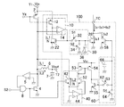
図8は、従来のスイッチングレギュレータの構成例を示す回路図である。図8のスイッチングレギュレータは、インダクタ電流検出回路900を有しており、特許文献1に開示されている。図9は、図8のスイッチングレギュレータにおける信号の波形を示すグラフである。図8において、入力端子T1には直流電圧Vinが入力されている。スイッチングトランジスタ2のゲートには、トランジスタ2をスイッチングする駆動信号が供給されている。整流トランジスタ4は、ドレインがトランジスタ2のドレインに接続されている。比較器5は、トランジスタ4のドレイン電圧と接地電位とを比較し、その結果を示す信号でトランジスタ4を駆動する。
FIG. 8 is a circuit diagram showing a configuration example of a conventional switching regulator. The switching regulator of FIG. 8 has an inductor
インダクタ6の一端は、トランジスタ2とトランジスタ4との接続点に接続されている。出力キャパシタ7は、インダクタ6の他端である出力端子T2に接続され、出力端子T2から負荷に出力電圧Voutが供給される。トランジスタ2に流れる電流をIL1とし、トランジスタ4に流れる電流をIL2とすると、インダクタ6に流れる電流はIL1+IL2となる。
One end of the
検出トランジスタ912のソース及びゲートは、トランジスタ2のソース及びゲートに接続されている。検出トランジスタ912のサイズはトランジスタ2の1/Nとする。差動増幅器914によって、トランジスタ2と検出トランジスタ912の各ドレイン電位が等しくなるようにトランジスタ922のドレイン−ソース間インピーダンスが調整されるので、トランジスタ912及び922には電流IL1/Nが流れる。トランジスタ928はトランジスタ922とカレントミラーを構成し、トランジスタ928にも電流IL1/Nが流れる。
The source and gate of the
検出トランジスタ942のドレイン及びゲートは、トランジスタ4のドレイン及びゲートに接続されている。検出トランジスタ942のサイズはトランジスタ4の1/Nとする。差動増幅器944によって、トランジスタ942のソース電位と接地電位とが等しくなるようにトランジスタ958のドレイン−ソース間インピーダンスが調整されるので、トランジスタ942及び958には電流IL2/Nが流れる。端子TCから流入する電流は(IL1+IL2)/Nとなるので、インダクタ電流IL1+IL2を検出することができる。
The drain and gate of the
しかしながら、図8の電流検出回路900では、トランジスタ2とトランジスタ4とがともにオフとなるデッドタイム等において、電流が検出されないという問題がある。例えば図9に示されているように、インダクタに流れる電流ILは連続であるが、電流検出回路900で得られる電流(IL1+IL2)/Nは不連続になってしまう。特にインダクタ電流の平均値を制御する平均カレントモード制御方式では、このような不連続な信号に従ってスイッチングレギュレータの制御を行うことは難しいという問題がある。
However, the
本発明は、スイッチングレギュレータのインダクタに流れる電流に応じた連続的な信号を得ることを目的とする。 An object of the present invention is to obtain a continuous signal corresponding to a current flowing through an inductor of a switching regulator.
本発明の実施形態による電流検出回路は、インダクタに接続され、電源から前記インダクタに流れる電流をスイッチングする第1のトランジスタと、前記インダクタ及び前記第1のトランジスタが接続されたノードに接続され、前記第1のトランジスタのオフ期間の一部においてオンになる第2のトランジスタとを有するスイッチングレギュレータの電流検出回路であって、前記第1のトランジスタを流れる電流に応じた検出電流を生成する電流生成回路と、前記第1のトランジスタのオン期間において前記検出電流に応じた電圧を出力し、前記第1のトランジスタのオフ期間において前記検出電流に応じた電圧を保持して出力する保持回路と、前記保持回路の出力電圧に応じた電流を生成する出力トランジスタとを有する。 A current detection circuit according to an embodiment of the present invention is connected to an inductor, connected to a first transistor that switches a current flowing from a power source to the inductor, and a node to which the inductor and the first transistor are connected, A current detection circuit for a switching regulator having a second transistor that is turned on in a part of an off period of the first transistor, wherein the current generation circuit generates a detection current corresponding to a current flowing through the first transistor A holding circuit that outputs a voltage corresponding to the detected current in an on period of the first transistor and holds and outputs a voltage corresponding to the detected current in an off period of the first transistor; And an output transistor for generating a current corresponding to the output voltage of the circuit.
これによると、第1のトランジスタのオフ期間では検出電流に応じた電圧を保持するので、第2のトランジスタの電流を検出することなく、インダクタに流れる電流に応じた連続的な信号を得ることができる。 According to this, since the voltage corresponding to the detected current is held in the off period of the first transistor, it is possible to obtain a continuous signal corresponding to the current flowing through the inductor without detecting the current of the second transistor. it can.
本発明の実施形態による他の電流検出回路は、インダクタに接続され、電源から前記インダクタに流れる電流をスイッチングする第1のトランジスタと、前記インダクタ及び前記第1のトランジスタが接続されたノードに接続され、前記第1のトランジスタのオフ期間の一部においてオンになる第2のトランジスタとを有するスイッチングレギュレータの電流検出回路であって、前記第2のトランジスタを流れる電流に応じた検出電流を生成する電流生成回路と、前記第2のトランジスタのオン期間において前記検出電流に応じた電圧を出力し、前記第2のトランジスタのオフ期間において前記検出電流に応じた電圧を保持して出力する保持回路と、前記保持回路の出力電圧に応じた電流を生成する出力トランジスタとを有する。 Another current detection circuit according to an embodiment of the present invention is connected to an inductor, and is connected to a first transistor that switches a current flowing from a power source to the inductor, and a node to which the inductor and the first transistor are connected. A current detection circuit of a switching regulator having a second transistor that is turned on during a part of an off period of the first transistor, and a current that generates a detection current according to a current flowing through the second transistor A generation circuit; and a holding circuit that outputs a voltage according to the detection current in an on period of the second transistor and holds and outputs a voltage according to the detection current in an off period of the second transistor; And an output transistor for generating a current corresponding to the output voltage of the holding circuit.
これによると、第2のトランジスタのオフ期間では検出電流に応じた電圧を保持するので、第1のトランジスタの電流を検出することなく、インダクタに流れる電流に応じた連続的な信号を得ることができる。 According to this, since the voltage corresponding to the detected current is held in the off period of the second transistor, it is possible to obtain a continuous signal corresponding to the current flowing through the inductor without detecting the current of the first transistor. it can.
本発明の実施形態による更に他の電流検出回路は、インダクタに接続され、電源から前記インダクタに流れる電流をスイッチングする第1のトランジスタと、前記インダクタ及び前記第1のトランジスタが接続されたノードに接続され、前記第1のトランジスタのオフ期間の一部においてオンになる第2のトランジスタとを有するスイッチングレギュレータの電流検出回路であって、前記第1のトランジスタを流れる電流に応じた第1の検出電流を生成する第1の電流生成回路と、前記第1のトランジスタのオン期間において前記第1の検出電流に応じた電圧を出力し、前記第1及び第2のトランジスタがともにオフである期間において前記第1の検出電流に応じた電圧を保持して出力する第1の保持回路と、前記第1の保持回路の出力電圧に応じた電流を生成する第1の出力トランジスタと、前記第2のトランジスタを流れる電流に応じた第2の検出電流を生成する第2の電流生成回路と、前記第2のトランジスタのオン期間において前記第2の検出電流に応じた電圧を出力し、前記第1及び第2のトランジスタがともにオフである期間において前記第2の検出電流に応じた電圧を保持して出力する第2の保持回路と、前記第2の保持回路の出力電圧に応じた電流を生成する第2の出力トランジスタとを有する。前記第1の出力トランジスタと前記第2の出力トランジスタとは並列に接続されている。 Still another current detection circuit according to an embodiment of the present invention is connected to an inductor, and is connected to a first transistor that switches a current flowing from a power source to the inductor, and a node to which the inductor and the first transistor are connected. And a second transistor that is turned on during a part of the off-period of the first transistor, and a first detection current corresponding to a current flowing through the first transistor. And a voltage corresponding to the first detection current in an on period of the first transistor, and the period in which both the first and second transistors are off. A first holding circuit that holds and outputs a voltage corresponding to the first detection current, and an output voltage of the first holding circuit A first output transistor that generates a current corresponding thereto, a second current generation circuit that generates a second detection current according to a current flowing through the second transistor, and the on-period of the second transistor A second holding circuit that outputs a voltage corresponding to the second detection current and holds and outputs a voltage corresponding to the second detection current in a period in which both the first and second transistors are off; And a second output transistor for generating a current corresponding to the output voltage of the second holding circuit. The first output transistor and the second output transistor are connected in parallel.
これによると、第1のトランジスタのオフ期間では第1の検出電流に応じた電圧を保持し、第2のトランジスタのオフ期間では第2の検出電流に応じた電圧を保持するので、デッドタイムにおいても出力信号の値が急変しない。したがって、インダクタに流れる電流に応じた連続的な信号を得ることができる。 According to this, since the voltage according to the first detection current is held in the off period of the first transistor and the voltage according to the second detection current is held in the off period of the second transistor, The output signal value does not change suddenly. Therefore, a continuous signal corresponding to the current flowing through the inductor can be obtained.
本発明の実施形態によるスイッチングレギュレータは、インダクタと、前記インダクタに接続され、電源から前記インダクタに流れる電流をスイッチングする第1のトランジスタと、前記インダクタ及び前記第1のトランジスタが接続されたノードに接続され、前記第1のトランジスタのオフ期間の一部においてオンになる第2のトランジスタと、電流検出回路とを有する。前記電流検出回路は、前記第1のトランジスタを流れる電流に応じた検出電流を生成する電流生成回路と、前記第1のトランジスタのオン期間において前記検出電流に応じた電圧を出力し、前記第1のトランジスタのオフ期間において前記検出電流に応じた電圧を保持して出力する保持回路と、前記保持回路の出力電圧に応じた電流を生成する出力トランジスタとを有する。 A switching regulator according to an embodiment of the present invention is connected to an inductor, a first transistor that is connected to the inductor and switches a current flowing from a power source to the inductor, and a node to which the inductor and the first transistor are connected. And a second transistor that is turned on during a part of the off-period of the first transistor, and a current detection circuit. The current detection circuit generates a detection current according to a current flowing through the first transistor, and outputs a voltage according to the detection current during an ON period of the first transistor, A holding circuit that holds and outputs a voltage corresponding to the detected current during an off period of the transistor, and an output transistor that generates a current corresponding to the output voltage of the holding circuit.
本発明の実施形態による他のスイッチングレギュレータは、インダクタと、前記インダクタに接続され、電源から前記インダクタに流れる電流をスイッチングする第1のトランジスタと、前記インダクタ及び前記第1のトランジスタが接続されたノードに接続され、前記第1のトランジスタのオフ期間の一部においてオンになる第2のトランジスタと、電流検出回路とを有する。前記電流検出回路は、前記第2のトランジスタを流れる電流に応じた検出電流を生成する電流生成回路と、前記第2のトランジスタのオン期間において前記検出電流に応じた電圧を出力し、前記第2のトランジスタのオフ期間において前記検出電流に応じた電圧を保持して出力する保持回路と、前記保持回路の出力電圧に応じた電流を生成する出力トランジスタとを有する。 Another switching regulator according to an embodiment of the present invention includes an inductor, a first transistor connected to the inductor and switching a current flowing from the power source to the inductor, and a node to which the inductor and the first transistor are connected. And a current detection circuit, and a second transistor that is turned on during a part of the off-period of the first transistor. The current detection circuit generates a detection current according to a current flowing through the second transistor, and outputs a voltage according to the detection current during an ON period of the second transistor, A holding circuit that holds and outputs a voltage corresponding to the detected current during an off period of the transistor, and an output transistor that generates a current corresponding to the output voltage of the holding circuit.
本発明の実施形態による更に他のスイッチングレギュレータは、インダクタと、前記インダクタに接続され、電源から前記インダクタに流れる電流をスイッチングする第1のトランジスタと、前記インダクタ及び前記第1のトランジスタが接続されたノードに接続され、前記第1のトランジスタのオフ期間の一部においてオンになる第2のトランジスタと、電流検出回路とを有する。前記電流検出回路は、前記第1のトランジスタを流れる電流に応じた第1の検出電流を生成する第1の電流生成回路と、前記第1のトランジスタのオン期間において前記第1の検出電流に応じた電圧を出力し、前記第1及び第2のトランジスタがともにオフである期間において前記第1の検出電流に応じた電圧を保持して出力する第1の保持回路と、前記第1の保持回路の出力電圧に応じた電流を生成する第1の出力トランジスタと、前記第2のトランジスタを流れる電流に応じた第2の検出電流を生成する第2の電流生成回路と、前記第2のトランジスタのオン期間において前記第2の検出電流に応じた電圧を出力し、前記第1及び第2のトランジスタがともにオフである期間において前記第2の検出電流に応じた電圧を保持して出力する第2の保持回路と、前記第2の保持回路の出力電圧に応じた電流を生成する第2の出力トランジスタとを有する。前記第1の出力トランジスタと前記第2の出力トランジスタとは並列に接続されている。 Still another switching regulator according to an embodiment of the present invention includes an inductor, a first transistor connected to the inductor and switching a current flowing from a power source to the inductor, and the inductor and the first transistor connected to each other. A second transistor connected to the node and turned on in a part of the off-period of the first transistor; and a current detection circuit. The current detection circuit generates a first detection current corresponding to a current flowing through the first transistor, and responds to the first detection current during an ON period of the first transistor. A first holding circuit that outputs and outputs a voltage corresponding to the first detection current in a period in which both the first and second transistors are off, and the first holding circuit A first output transistor that generates a current according to the output voltage of the first transistor, a second current generation circuit that generates a second detection current according to a current flowing through the second transistor, and A voltage corresponding to the second detection current is output in the on period, and a voltage corresponding to the second detection current is held and output in a period in which both the first and second transistors are off. It has a second holding circuit, and a second output transistor for generating a current corresponding to the output voltage of the second holding circuit. The first output transistor and the second output transistor are connected in parallel.
本発明の実施形態によれば、インダクタに流れる電流に応じた連続的な信号を得ることができる。また、得られた信号を用いて例えば平均カレントモード制御をスイッチングレギュレータに対して行うことにより、スイッチングノイズによる誤動作のない出力電圧の安定化制御が可能となる。 According to the embodiment of the present invention, a continuous signal corresponding to the current flowing through the inductor can be obtained. Further, by performing, for example, average current mode control on the switching regulator using the obtained signal, it is possible to control the stabilization of the output voltage without malfunction due to switching noise.
以下、本発明の実施形態を、図面を参照しながら説明する。図面において下2桁が同じ参照番号で示された構成要素は、互いに対応しており、同一の又は類似の構成要素である。 Embodiments of the present invention will be described below with reference to the drawings. In the drawings, the components indicated by the same reference numerals in the last two digits correspond to each other and are the same or similar components.
(第1の実施形態)
図1は、本発明の第1の実施形態に係る電流検出回路を有するスイッチングレギュレータの構成例を示す回路図である。図1のスイッチングレギュレータは、スイッチングトランジスタ2と、整流トランジスタ4と、比較器5と、インダクタ6と、出力キャパシタ7と、AND回路8と電流検出回路100とを有している。スイッチングトランジスタ2及び整流トランジスタ4は、図1のスイッチングレギュレータの出力回路を構成している。
(First embodiment)
FIG. 1 is a circuit diagram showing a configuration example of a switching regulator having a current detection circuit according to the first embodiment of the present invention. The switching regulator in FIG. 1 includes a switching
電流検出回路100は、電流生成回路10,40と、補助トランジスタ22,52と、出力トランジスタ28,58と、保持回路30,60と、PMOSFET(p-channel Metal Oxide Semiconductor Field-Effect Transistor)53,54と、NMOSFET(n-channel Metal Oxide Semiconductor Field-Effect Transistor)55とを有している。電流生成回路10は、検出トランジスタ12と、差動増幅器14とを有している。保持回路30は、スイッチ32と、補助スイッチ34と、キャパシタ36とを有している。電流生成回路40は、検出トランジスタ42と、差動増幅器44とを有している。保持回路60は、スイッチ62と、補助スイッチ64と、キャパシタ66とを有している。
The
入力端子T1には、バッテリー等の電源が接続され、直流電圧Vinが入力される。スイッチングトランジスタ2は、PMOSFETであって、そのソースは入力端子T1に接続され、ゲートにはスイッチングトランジスタ2をスイッチングする駆動信号Vgが入力されている。インダクタ6の一端は、スイッチングトランジスタ2のドレインに接続されている。整流トランジスタ4はNMOSFETであって、そのドレインはスイッチングトランジスタ2とインダクタ6とが接続されたノードに接続されている。整流トランジスタ4のソースは接地されている。出力キャパシタ7は、インダクタ6の他端である出力端子T2に接続されている。出力キャパシタ7は、出力電圧Voutを平滑化して、出力端子T2から負荷に供給する。
A power source such as a battery is connected to the input terminal T1, and a DC voltage Vin is input thereto. The switching
スイッチングトランジスタ2と整流トランジスタ4とは交互にオンになり、インダクタ6にインダクタ電流を流して出力キャパシタ7へ電流を供給する。ここで、スイッチングの際にスイッチングトランジスタ2及び整流トランジスタ4が同時にオンする期間が発生しないように、スイッチングトランジスタ2及び整流トランジスタ4がともにオフであるデッドタイム期間が設けられる。このため、実際には整流トランジスタ4は、スイッチングトランジスタ2のオフ期間の一部においてオンになる。スイッチングトランジスタ2からインダクタ6へ流れるインダクタ電流をIL1、整流トランジスタ4からインダクタ6へ流れるインダクタ電流をIL2とする。電流検出回路100は、インダクタ電流IL=IL1+IL2にほぼ比例する電流Isを生成する。
The switching
比較器5は、整流トランジスタ4のドレイン電圧を接地電位と比較し、比較結果をAND回路8に出力する。AND回路8は、比較器5の出力と制御信号S2との論理和を求め、整流トランジスタ4のゲートに出力する。
The
このような構成により、整流トランジスタ4は整流機能を有する。すなわち、整流トランジスタ4のソースからドレインに電流が流れるとき、電圧降下によって整流トランジスタ4のドレイン電圧は接地電圧を下回るので、比較器5はHレベルを出力して整流トランジスタ4をオンにする。このとき、制御信号S2はHレベル、駆動信号Vg2はLレベルであるとする。一方、逆方向に電流が流れようとすると、比較器5はLレベルを出力して整流トランジスタ4をオフにする。
With such a configuration, the rectifying
図1の電流検出回路100において、第1の検出トランジスタ12は、PMOSFETであって、そのソース及びゲートがスイッチングトランジスタ2のソース及びゲートにそれぞれ接続され、スイッチングトランジスタ2に同期して同様に動作する。第1の検出トランジスタ12のサイズは、スイッチングトランジスタ2のサイズの1/Nであるとする。Nの値は、例えば数千〜数万である。トランジスタのサイズは、例えばトランジスタのゲート幅や、ゲート幅/ゲート長を意味する。トランジスタ22のサイズとトランジスタ28のサイズとは等しいとする。
In the
第1の検出トランジスタ12の電流はNMOSFETである補助トランジスタ22に流れる。差動増幅器14は、スイッチングトランジスタ2及び第1の検出トランジスタ12のそれぞれのドレイン電位の差を増幅して、補助トランジスタ22のゲートに出力する。この構成によって、スイッチングトランジスタ2及び第1の検出トランジスタ12の各ドレイン電位が等しくなるように補助トランジスタ22のドレイン−ソース間インピーダンスが調整されるので、トランジスタ12は、電流IL1に精度良く比例する電流IL1/Nを生成する。補助トランジスタ22にも電流IL1/Nが流れる。
The current of the
トランジスタ28のゲートは、スイッチ32を介してトランジスタ22のゲートと接続され、トランジスタ28とトランジスタ22とはカレントミラーを構成する。スイッチ32がオンのとき、トランジスタ28にはトランジスタ22と同じく電流IL1/Nが流れる。トランジスタ28のゲート−ソース間には補助スイッチ34とキャパシタ36とが並列に接続され、トランジスタ28のドレインは出力端子TCに接続されている。スイッチ32及び補助スイッチ34は、それぞれ制御信号S1,S2に従って動作する。
The gate of the transistor 28 is connected to the gate of the
NMOSFETである第2の検出トランジスタ42は、そのドレイン及びゲートが整流トランジスタ4のドレイン及びゲートにそれぞれ接続され、整流トランジスタ4に同期して同様に動作する。第2の検出トランジスタ42のサイズは、整流トランジスタ4のサイズの1/Nであるとする。また、トランジスタ42のサイズとトランジスタ52のサイズとは等しいとする。トランジスタ53のサイズとトランジスタ54のサイズとは等しいとする。トランジスタ55のサイズとトランジスタ58のサイズとは等しいとする。
The
差動増幅器44は、トランジスタ42のソース電位と接地電位との差を増幅して、補助トランジスタ52のゲートに出力する。トランジスタ52のソースはトランジスタ42のソースに接続され、トランジスタ52のドレインはPMOSFETであるトランジスタ53のゲート及びドレインに接続される。
The
トランジスタ53はトランジスタ54とカレントミラーを構成し、トランジスタ53及びトランジスタ54のソースは入力端子T1に接続されている。トランジスタ54のドレインは、NMOSFETであるトランジスタ55のドレイン及びゲートに接続されている。トランジスタ55のソースは接地されている。この構成によって、トランジスタ42のソース電位と接地電位とが等しくなるように補助トランジスタ52のドレイン−ソース間インピーダンスが調整されるので、トランジスタ42は、電流IL2に精度良く比例する電流IL2/Nを生成する。補助トランジスタ52にも電流IL2/Nが流れる。
The
トランジスタ53及びトランジスタ54のカレントミラーによってトランジスタ54のドレインからも電流IL2/Nが流れ、この電流は更にトランジスタ55を流れる。トランジスタ58のゲートは、スイッチ62を介してトランジスタ55のゲートと接続され、トランジスタ58とトランジスタ55とはカレントミラーを構成する。スイッチ62がオンのとき、トランジスタ58にはトランジスタ55と同じく電流IL2/Nが流れる。トランジスタ58のゲート−ソース間には補助スイッチ64とキャパシタ66とが並列に接続され、トランジスタ58のドレインは出力端子TCに接続されている。スイッチ62及び補助スイッチ64は、それぞれ制御信号S3,S4に従って動作する。
The current IL2 / N also flows from the drain of the
以上のような電流生成回路10,40は一例であって、それぞれ電流IL1,IL2に比例する電流を生成する回路であれば、他の構成を有していてもよい。
The
図2は、図1のスイッチングレギュレータにおける信号の波形を示すグラフである。図2には、スイッチングトランジスタ2への駆動信号Vg、インダクタ6に流れる電流IL、第1の検出トランジスタ12を流れる検出電流IL1/N、第2の検出トランジスタ42を流れる検出電流IL2/N、スイッチ32の制御信号S1、補助スイッチ34の制御信号S2、スイッチ62の制御信号S3、補助スイッチ64の制御信号S4、トランジスタ28を流れる検出電流Is1、トランジスタ58を流れる検出電流Is2、及び出力端子TCから流入する検出電流Is1+Is2が示されている。図1及び図2を参照して、図1の電流検出回路の動作を説明する。
FIG. 2 is a graph showing signal waveforms in the switching regulator of FIG. In FIG. 2, the drive signal Vg to the switching
スイッチ32,62及び補助スイッチ34,64は、それぞれに入力される制御信号がHレベルのときにオンになる。スイッチングトランジスタ2はPチャンネルトランジスタなので、駆動信号VgがLレベルのときにオンになる。これと連動して検出電流IL1/Nを流すために、スイッチ32の制御信号S1は駆動信号Vgの反転信号とする。一方、補助スイッチ34の制御信号S2は、制御信号S1のLレベルの期間及びその前後のデッドタイム期間にLレベルとなる。すなわち、制御信号S2は、整流トランジスタ4を駆動する比較器5の出力に同期する。
The
スイッチングトランジスタ2のオン期間において、スイッチ32がオンになり、出力トランジスタ28のゲートには、トランジスタ22のゲート電圧、すなわち、電流Is1(=IL1/N)に応じた電圧が与えられる。出力トランジスタ28は、ゲートに与えられた電圧に応じた電流Is1を生成する。
In the on period of the switching
スイッチ32がターンオフ後のデッドタイム期間中には、キャパシタ36は出力トランジスタ28のゲート電圧を保持する。このため、デッドタイム期間中も出力トランジスタ28には電流Is1が流れ続ける。デッドタイム期間が終了して整流トランジスタ4がターンオンすると同時に補助スイッチ34がオンとなり、出力トランジスタ28のゲートは接地されるので、出力トランジスタ28には電流Is1が流れなくなる。
During the dead time period after the
スイッチ62の制御信号S3は制御信号S2に等しく、補助スイッチ64の制御信号S4は制御信号S1に等しい。整流トランジスタ4のオン期間において、スイッチ62がオンになり、出力トランジスタ58のゲートには、トランジスタ55のゲート電圧、すなわち、電流Is2(=IL2/N)に応じた電圧が与えられる。出力トランジスタ58は、ゲートに与えられた電圧に応じた電流Is2を生成する。
The control signal S3 of the
スイッチ62がターンオフ後のデッドタイム期間中には、キャパシタ66は出力トランジスタ58のゲート電圧を保持する。このため、デッドタイム期間中も出力トランジスタ58には電流Is2が流れ続ける。デッドタイム期間が終了してスイッチングトランジスタ2がターンオンすると同時に補助スイッチ64がオンとなり、出力トランジスタ58のゲートは接地されるので、出力トランジスタ58には電流Is2が流れなくなる。
During the dead time period after the
図2に示されているように、出力トランジスタ28及び58のドレインが接続される出力端子TCから流入する電流Is(=Is1+Is2)は、デッドタイム期間中にも保持される。スイッチングトランジスタ2がスイッチングする毎に電流Isがゼロになることがないので、インダクタ電流ILに高精度に比例する連続的な信号である電流Isを生成することができる。
As shown in FIG. 2, the current Is (= Is1 + Is2) flowing from the output terminal TC to which the drains of the
(第2の実施形態)
図3は、本発明の第2の実施形態に係る電流検出回路を有するスイッチングレギュレータの構成例を示す回路図である。図3のスイッチングレギュレータは、電流検出回路100に代えて電流検出回路200を有し、平均化回路70と、駆動信号生成部80と、誤差増幅器91と、基準電圧源92と、抵抗93とを更に有している点が、図1のスイッチングレギュレータとは異なっている。図3のスイッチングレギュレータは、出力端子TCから出力される検出電流Isを用いて、出力端子T2から出力される出力電圧Voutを安定化制御する。
(Second Embodiment)
FIG. 3 is a circuit diagram showing a configuration example of a switching regulator having a current detection circuit according to the second embodiment of the present invention. The switching regulator of FIG. 3 includes a
電流検出回路200は、電流生成回路10と、補助トランジスタ22と、NMOSFET22と、PMOSFET24と、PMOSFETである出力トランジスタ29と、保持回路230とを有している。電流生成回路10及び補助トランジスタ22は、図1を参照して説明したものと同様である。保持回路230は、スイッチ32と、キャパシタ36とを有している。
The
補助トランジスタ22とトランジスタ23とは、カレントミラーを構成している。PMOSFET24と出力トランジスタ29とは、カレントミラーを構成している。補助トランジスタ22のサイズとトランジスタ23のサイズとは等しいとする。トランジスタ24のサイズと出力トランジスタ29のサイズとは等しいとする。
The
出力トランジスタ29のゲートは、スイッチ32を介してトランジスタ24のゲートと接続されている。スイッチ32がオンのとき、出力トランジスタ29にはトランジスタ24と同じく電流IL1/Nが流れ、この電流が検出電流Isとして出力端子TCから出力される。出力トランジスタ29のゲート−ソース間にはキャパシタ36が並列に接続され、トランジスタ29のドレインは出力端子TCに接続されている。スイッチ32は、制御信号S1に従って動作する。
The gate of the
平均化回路70は、オペアンプ72と、基準電圧Vr2を出力する基準電圧源74と、キャパシタ76と、抵抗78とを有している。駆動信号生成部80は、三角波発生器82と、PWM比較器84と、インバータ86とを有している。
The averaging
誤差増幅器91は、出力電圧Voutと目標電圧である基準電圧源92の基準電圧Vr1との差を増幅して、出力電圧Voutと基準電圧Vr1との間の誤差を示す誤差信号を生成し、抵抗93を介してオペアンプ72に出力する。オペアンプ72は、入力された信号を平滑化して、平均化信号VaとしてPWM比較器84に出力する。三角波発生器82は、三角波電圧Vtを発生する。PWM比較器84は、平均化信号Vaと三角波電圧Vtとに基づいてパルス電圧を生成する。インバータ86は、パルス電圧を反転して駆動信号Vgとして出力する。駆動信号Vgは、スイッチングトランジスタ2に与えられる。
The
以上の構成で行われる平均カレントモード制御と呼ばれる制御について説明する。まず、電流Isはインダクタ6に流れる電流を示す検出電流であるとし、誤差増幅器91から出力される誤差信号の電圧をVe、抵抗93の抵抗値をRiとすると、オペアンプ72の反転入力端子には電圧(Ve+Ri×Is)が与えられる。オペアンプ72は、この反転入力端子の電圧と基準電圧Vr2との差を平滑化及び増幅し、得られた平均化信号Vaを出力する。
A control called average current mode control performed in the above configuration will be described. First, assuming that the current Is is a detection current indicating the current flowing through the
PWM比較器84は、平均化信号Vaと三角波電圧Vtとを比較し、比較結果をパルス電圧として出力する。このパルス電圧の1周期に占めるHレベルの期間の割合は、スイッチングトランジスタ2の1周期に占めるオン時間の割合であるデューティ比Dに等しい。三角波電圧Vtが一定の周期で電圧0〜Etの間での増減を繰り返すとすると、デューティ比Dは、
D=Va/Et
で表される。
The
D = Va / Et
It is represented by
例えば、出力端子T2からの出力電流が減少したり、入力電圧Vinが上昇したりすると、出力電圧Voutも上昇する。上昇した出力電圧Voutが基準電圧Vr1を越えると、誤差電圧Veは上昇する。誤差電圧Veの上昇によって、オペアンプ72の反転入力端子に与えられる電圧も上昇し、オペアンプ72が出力する平均化信号Vaは低下する。平均化信号Vaの低下に伴い、デューティ比Dは低下する。すなわちスイッチングトランジスタ2のオン時間が短縮されるため、インダクタ6に蓄えられる励磁エネルギーは減少し、インダクタ6を流れる電流は減少する。
For example, when the output current from the output terminal T2 decreases or the input voltage Vin increases, the output voltage Vout also increases. When the increased output voltage Vout exceeds the reference voltage Vr1, the error voltage Ve increases. As the error voltage Ve increases, the voltage applied to the inverting input terminal of the
このため、インダクタ6を介して出力端子T2へ供給される電力が減少するので、上昇した出力電圧Voutを低下させるように負帰還がかかる。誤差電圧Veの上昇によってインダクタ6を流れる電流が減少する関係は、平均化回路70におけるオペアンプ72の入力のイマジナリーショートを考慮して、
Ve+Ri×Is=Vr2
のように表される。つまり、誤差電圧Veの変動に対し検出電流Isが逆に変動する。
For this reason, since the electric power supplied to the output terminal T2 via the
Ve + Ri × Is = Vr2
It is expressed as That is, the detection current Is fluctuates in reverse with respect to the fluctuation of the error voltage Ve.
ここで、キャパシタ76及び抵抗78によって、検出電流Isに重畳している交流分が減衰されているので、検出電流Isの平均値が誤差電圧Veの変動に従って変動する。また、負帰還によって出力電圧Voutは基準電圧Vr1に等しくなる。
Here, since the AC component superimposed on the detection current Is is attenuated by the
図4は、図3のスイッチングレギュレータにおける信号の波形を示すグラフである。図4には、スイッチングトランジスタ2への駆動信号Vg、インダクタ6に流れる電流IL、検出トランジスタ12を流れる検出電流IL1/N、スイッチ32の制御信号S1、出力トランジスタ29を流れる検出電流Is、三角波電圧Vt、及び平均化信号Vaが示されている。図3及び図4を参照して、図3の電流検出回路200の動作を説明する。
FIG. 4 is a graph showing signal waveforms in the switching regulator of FIG. FIG. 4 shows the drive signal Vg to the switching
スイッチングトランジスタ2はPチャンネルトランジスタなので、駆動信号VgがLレベルのときにオンとなる。これと連動して検出電流IL1/Nを流すために、スイッチ32の制御信号S1は駆動信号Vgの反転信号とする。
Since the switching
スイッチングトランジスタ2のオン期間において、スイッチ32がオンになり、出力トランジスタ29のゲートには、トランジスタ22のゲート電圧、すなわち、電流Is(=IL1/N)に応じた電圧が与えられる。出力トランジスタ29は、ゲートに与えられた電圧に応じた電流Isを生成する。
In the on period of the switching
スイッチ32がターンオフしてから再びオンするまでの期間、すなわちスイッチングトランジスタ2のオフ期間には、キャパシタ36は出力トランジスタ29のゲート電圧を保持する。このため、オフ期間中も出力トランジスタ29には電流Isが流れ続ける。したがって、検出電流Isは、実際のインダクタ電流ILとは、スイッチングトランジスタ2のオン期間だけ比例関係にあり、検出電流Isはインダクタ電流ILに近似した波形を有する。しかし、平均カレントモード制御においては、厳密にインダクタ電流を検出する必要はなく、インダクタ電流ILのおおよそのレベルを検出制御することによっても出力電圧Voutの制御が可能である。
The
このような平均カレントモード制御方法は、インダクタ電流を平均化した信号を用いて駆動信号を生成するので、スイッチングノイズの影響を受け難いという特徴がある。しかし、第1の実施形態のようにスイッチングトランジスタ2と整流トランジスタ4との両方の電流を検出して加算する場合には、各トランジスタ電流を検出する回路においてミラー比の不一致があると、電流の急峻な変動が生じてしまう。その変動の影響は平均化しても取り除くことはできず、チャタリングのような誤作動の危険性が生じる。
Such an average current mode control method is characterized in that the drive signal is generated using a signal obtained by averaging the inductor current, so that it is hardly affected by switching noise. However, when the currents of both the switching
これに対し、本実施形態のように、スイッチングトランジスタ2のオン期間のみインダクタ電流を検出し、オフ期間は検出電流値を保持すると、検出電流の急変はターンオン時に限定される。しかもその影響は、図4に示すように、平均化信号Vaが三角波電圧Vtを上回った直後に急増することとして現れるので、むしろチャタリング等が防止され、スイッチングレギュレータの動作が安定する。
On the other hand, when the inductor current is detected only during the ON period of the switching
以上のように本実施形態の電流検出回路によれば、スイッチングトランジスタ2のオン時の電流を検出した後、オフ時には検出値を保持することによって近似的にインダクタ電流を検出することができる。
As described above, according to the current detection circuit of this embodiment, after detecting the current when the switching
(第2の実施形態の変形例)
第2の実施形態のように、スイッチングトランジスタ2のオン時の電流を検出した後、オフ時には検出値を保持することによって近似的にインダクタ電流を検出する場合には、デューティ比がゼロになると要注意である。なぜなら、実際のインダクタ電流ILは減少していくのに対し、検出電流Isは保持されたままだからである。
(Modification of the second embodiment)
As in the second embodiment, after detecting the current when the switching
図5は、第2の実施形態の変形例に係る電流検出回路を有するスイッチングレギュレータの構成例を示す回路図である。図5のスイッチングレギュレータは、駆動信号生成部80に代えて駆動信号生成部380を有している点が、図3のスイッチングレギュレータとは異なっている。駆動信号生成部380は、三角波発生器82と、基準電圧源383と、PWM比較器384と、NAND回路386と、オフセット電圧源387と、ヒステリシス比較器388とを有している。
FIG. 5 is a circuit diagram showing a configuration example of a switching regulator having a current detection circuit according to a modification of the second embodiment. The switching regulator of FIG. 5 is different from the switching regulator of FIG. 3 in that a driving
PWM比較器384は、基準電圧源383の電圧が与えられる非反転入力端子を更に有している点が、PWM比較器84とは異なっている。ヒステリシス比較器388は、基準電圧Vr1にオフセット電圧源387の電圧が加算された基準電圧Vr3と、出力電圧Voutとを比較する。ヒステリシス比較器388のヒステリシスは、オフセット電圧源387の電圧又はそれに近い値に設定される。NAND回路386は、PWM比較器384の比較結果と、ヒステリシス比較器388の比較結果との論理和を駆動信号Vgとして出力する。
The
PWM比較器384は、2つの非反転入力のうちの電位が高い方を優先して用いるものとし、基準電圧源383の電圧は、三角波電圧Vtの波形と所定の低電位で交差するように設定される。PWM比較器384は、平均化信号Vaが基準電圧源383の電圧より小さい場合には、基準電圧源383の電圧と三角波電圧Vtの波形との交点で決まる幅を有するパルスを出力する。つまり、平均化信号Vaがどんなに低下しても、PWM比較器384が出力するパルスの幅は、所定値より小さくならない。言い換えると、PWM比較器384は、スイッチングトランジスタ2のオン期間の長さが所定の閾値以上となるように(デューティ比が最小デューティ比Dmin以上となるように)、パルスを出力する。ヒステリシス比較器388がHレベルを出力しているときには、NAND回路386は、PWM比較器384の出力信号を反転させて、駆動信号Vgとして出力する。
The
図5のスイッチングレギュレータは、電流検出回路200がインダクタ電流を近似的に検出し、これを用いて平均カレントモード制御によって出力電圧Voutを安定化制御する点は、図3のスイッチングレギュレータと同様である。ところが、デューティ比が非常に小さくなる軽負荷時には、以下のように動作する。
The switching regulator of FIG. 5 is similar to the switching regulator of FIG. 3 in that the
まず、軽負荷であっても、出力電圧Voutを安定化するために、出力端子T2へ供給するインダクタ電流を減少しようとして平均化信号Vaが低下する。ところが、基準電圧源383の電圧で設定される最小デューティ比Dmin以下にはならないので、出力端子T2への供給電力が過剰となり、出力電圧Voutは目標電圧である基準電圧Vr1を越えて増加する。出力電圧Voutが基準電圧Vr3を越えると、ヒステリシス比較器388はLレベルを出力し、NAND回路386を介して駆動信号VgをHレベルにしてスイッチングトランジスタ2をオフにする。
First, in order to stabilize the output voltage Vout even when the load is light, the average signal Va is lowered in an attempt to reduce the inductor current supplied to the output terminal T2. However, since it is not less than the minimum duty ratio Dmin set by the voltage of the
スイッチングトランジスタ2のオフ状態ではインダクタ電流の出力端子T2への供給はなくなり、出力電圧Voutは低下していく。出力電圧Voutが基準電圧Vr1まで下がると、ヒステリシス比較器388は出力をHレベルに戻す。このとき、PWM比較器384が平均化信号Vaと三角波電圧Vtとを比較することによって駆動信号VgがNAND回路386を介して出力されるようになる。この駆動信号Vgによってスイッチングトランジスタ2はスイッチング動作を再開する。出力端子T2からの供給電力が軽負荷状態のままであれば、最小デューティ比Dminでのスイッチング動作によって再び出力電圧Voutは上昇し、上記動作を繰り返す。
When the switching
なお、ヒステリシス比較器388によるスイッチング動作の停止期間には、図5のスイッチングレギュレータを構成する各回路の動作を必要最小限となるようにして、低消費電力化を図ってもよい。
Note that, during the stop period of the switching operation by the
以上のように図5のスイッチングレギュレータによれば、最小デューティ比Dminを設定するので、実際のインダクタ電流ILは減少していくのに、検出電流Isは保持されたままという状態を回避することができる。また、そのために発生する軽負荷時の出力電圧Voutの上昇をヒステリシス比較器383によって検出し、検出された場合にはスイッチング動作を停止する。このことにより、出力電圧Voutの過電圧状態を回避するとともに、停止期間があるので軽負荷時の低消費電力化も達成できる。
As described above, according to the switching regulator of FIG. 5, since the minimum duty ratio Dmin is set, it is possible to avoid a state in which the detected current Is is held while the actual inductor current IL is decreased. it can. Further, the
(第3の実施形態)
図3及び図5のスイッチングレギュレータでは、スイッチングトランジスタのオン時の電流を検出した後、オフ時には検出値を保持するが、本実施形態では、整流トランジスタの電流を検出した後、スイッチングトランジスタのオン時には検出値を保持するような電流検出方法について説明する。
(Third embodiment)
In the switching regulators of FIGS. 3 and 5, the detected value is retained when the switching transistor is turned on after being detected, but in this embodiment, the current of the rectifying transistor is detected and then the switching transistor is turned on. A current detection method for holding the detection value will be described.
図6は、本発明の第3の実施形態に係る電流検出回路を有するスイッチングレギュレータの構成例を示す回路図である。図6のスイッチングレギュレータは、電流検出回路200及び駆動信号生成部80に代えて電流検出回路400及び駆動信号生成部480を有する点が、図3のスイッチングレギュレータとは異なっている。図5のスイッチングレギュレータは、出力端子TCから出力される検出電流Isを用いて、出力端子T2から出力される出力電圧Voutを安定化制御する。
FIG. 6 is a circuit diagram showing a configuration example of a switching regulator having a current detection circuit according to the third embodiment of the present invention. The switching regulator of FIG. 6 is different from the switching regulator of FIG. 3 in that it includes a
電流検出回路400は、電流生成回路40と、補助トランジスタ52と、PMOSFET53と、PMOSFETである出力トランジスタ59と、保持回路460とを有している。電流生成回路40、補助トランジスタ52、及びPMOSFET53は、図1を参照して説明したものと同様である。
The
出力トランジスタ59のゲートは、スイッチ62を介してトランジスタ53のゲートと接続されている。トランジスタ53と出力トランジスタ59とはカレントミラーを構成している。トランジスタ53のサイズと出力トランジスタ59のサイズとは等しいとする。スイッチ62がオンのとき、出力トランジスタ59にはトランジスタ53と同じく電流IL2/Nが流れる。出力トランジスタ59のゲート−ソース間にはキャパシタ66が並列に接続され、出力トランジスタ59のドレインは出力端子TCに接続されている。スイッチ62は、制御信号S3に従って動作する。
The gate of the
駆動信号生成部480は、三角波発生器82と、基準電圧源483と、PWM比較器484と、インバータ86とを有している。PWM比較器484は、基準電圧源483の電圧Vr4が与えられる非反転入力端子を更に有している点が、PWM比較器84とは異なっている。
The drive
PWM比較器484は、2つの非反転入力のうちの電位が低い方を優先して用いるものとし、基準電圧源483の電圧Vr4は、三角波電圧Vtの波形と所定の高電位で交差するように設定される。PWM比較器484は、平均化信号Vaが電圧Vr4より大きい場合には、電圧Vr4と三角波電圧Vtの波形との交点で決まる幅を有するパルスを出力する。つまり、平均化信号Vaがどんなに上昇しても、PWM比較器484が出力するパルスの幅は、所定値より大きくならない。言い換えると、PWM比較器484は、スイッチングトランジスタ2のオン期間の長さが所定の閾値以下となるように(デューティ比が最大デューティ比Dmax以下となるように)、パルスを出力する。インバータ86は、PWM比較器484の出力信号を反転させて、駆動信号Vgとして出力する。
The
図6のスイッチングレギュレータは、電流検出回路400がインダクタ電流を近似的に検出し、これを用いて平均カレントモード制御によって出力電圧Voutを安定化制御する点は、図3のスイッチングレギュレータと同様である。
The switching regulator of FIG. 6 is similar to the switching regulator of FIG. 3 in that the
次に、電流検出回路400が、インダクタ6を流れる電流ILをこれに近似した検出電流Isとして検出する動作を説明する。図7は、図6のスイッチングレギュレータにおける信号の波形を示すグラフである。図7には、スイッチングトランジスタ2への駆動信号Vg、整流トランジスタ4への駆動信号Vgl、インダクタ6に流れる電流IL、検出トランジスタ42を流れる検出電流IL1/N、スイッチ62の制御信号S3、出力トランジスタ59を流れる検出電流Is、三角波電圧Vt、及び平均化信号Vaが示されている。図6及び図7を参照して、図6の電流検出回路400の動作を説明する。
Next, the operation in which the
整流トランジスタ4はNチャンネルトランジスタなので、駆動信号VglがHレベルのときにオンとなる。これと連動して検出電流IL2/Nを流すために、スイッチ62の制御信号S3は駆動信号Vglと同じ信号とする。
Since the rectifying
整流トランジスタ4のオン期間において、スイッチ62がオンになり、出力トランジスタ59のゲートには、トランジスタ53のゲート電圧、すなわち、電流Is(=IL2/N)に応じた電圧が与えられる。出力トランジスタ59は、ゲートに与えられた電圧に応じた電流Isを生成する。
During the ON period of the rectifying
スイッチ62がターンオフしてから再びオンするまでの期間、すなわち整流トランジスタ4のオフ期間には、キャパシタ66は出力トランジスタ59のゲート電圧を保持する。このため、オフ期間中も出力トランジスタ59には電流Isが流れ続ける。したがって、検出電流Isは、実際のインダクタ電流ILとは、整流トランジスタ4のオン期間だけ比例関係にあり、検出電流Isはインダクタ電流ILに近似した波形を有する。しかし、平均カレントモード制御においては、厳密にインダクタ電流を検出する必要はなく、インダクタ電流ILのおおよそのレベルを検出制御することによっても出力電圧Voutの制御が可能である。
The
本実施形態のように、整流トランジスタ4のオン期間のみインダクタ電流を検出し、オフ期間は検出電流値を保持すると、検出電流の急変はスイッチングトランジスタ2のターンオフ時に限定される。しかもその影響は、図7に示すように、平均化信号が三角波電圧Vtを下回った直後に急減することとして現れるので、むしろチャタリング等が防止され、スイッチングレギュレータの動作が安定する。
As in the present embodiment, if the inductor current is detected only during the on period of the rectifying
さて、本実施形態のように、スイッチングトランジスタのオフ時の電流を検出した後、オン時には検出値を保持することによって近似的にインダクタ電流を検出する場合、デューティ比が1になると要注意である。なぜなら、実際のインダクタ電流ILは増加していくのに対し、検出電流Isは保持されたままだからである。PWM比較器484が出力するパルスのデューティ比が最大デューティ比Dmax以下となるようにしたのはこのためである。
Now, as in this embodiment, after detecting the current when the switching transistor is off, when the inductor current is approximately detected by holding the detection value when the switching transistor is on, it is necessary to pay attention to the duty ratio of 1. . This is because the actual inductor current IL increases while the detected current Is remains held. This is the reason why the duty ratio of the pulse output from the
以上のように本実施形態の電流検出回路によれば、整流トランジスタ4のオン時の電流を検出した後、オフ時には検出値を保持することによって近似的にインダクタ電流を検出することができる。
As described above, according to the current detection circuit of this embodiment, after detecting the current when the rectifying
以上の各実施形態においては、電流検出回路が降圧型スイッチングレギュレータの電流を検出する場合を例として説明したが、本発明はこの構成には限定されない。本発明の電流検出回路は、直列接続された2つのスイッチの接続点から連続的に電流を出力するスイッチングレギュレータに対して同様に適用することができる。すなわち、本発明は、降圧型に限らず、昇圧型や反転型のスイッチングレギュレータにも適用することができる。 In each of the above embodiments, the case where the current detection circuit detects the current of the step-down switching regulator has been described as an example, but the present invention is not limited to this configuration. The current detection circuit of the present invention can be similarly applied to a switching regulator that continuously outputs current from the connection point of two switches connected in series. That is, the present invention can be applied not only to a step-down type but also to a step-up type or an inverting type switching regulator.
本発明の多くの特徴及び優位性は、記載された説明から明らかであり、よって添付の特許請求の範囲によって、本発明のそのような特徴及び優位性の全てをカバーすることが意図される。更に、多くの変更及び改変が当業者には容易に可能であるので、本発明は、図示され記載されたものと全く同じ構成及び動作に限定されるべきではない。したがって、全ての適切な改変物及び等価物は本発明の範囲に入るものとされる。 The many features and advantages of the present invention are apparent from the written description, and thus, it is intended by the appended claims to cover all such features and advantages of the invention. Further, since many changes and modifications will readily occur to those skilled in the art, the present invention should not be limited to the exact construction and operation as illustrated and described. Accordingly, all suitable modifications and equivalents are intended to be within the scope of the present invention.
以上説明したように、本発明の実施形態によると、インダクタに流れる電流に応じた連続的な信号を得ることができるので、本発明は、電流検出回路及びスイッチングレギュレータ等について有用である。 As described above, according to the embodiment of the present invention, since a continuous signal corresponding to the current flowing through the inductor can be obtained, the present invention is useful for a current detection circuit, a switching regulator, and the like.
10,40 電流生成回路
22,52 補助トランジスタ
28,29,58,59 出力トランジスタ
30,60,230,460 保持回路
32,62 スイッチ
34,64 補助スイッチ
36,66 キャパシタ
70 平均化回路
80,380,480 駆動信号生成部
82 三角波発生器
84,384,484 PWM比較器
91 誤差増幅器
100,200,400 電流検出回路
10, 40
Claims (17)
前記第1のトランジスタを流れる電流に応じた検出電流を生成する電流生成回路と、
前記第1のトランジスタのオン期間において前記検出電流に応じた電圧を出力し、前記第1のトランジスタのオフ期間において前記検出電流に応じた電圧を保持して出力する保持回路と、
前記保持回路の出力電圧に応じた電流を生成する出力トランジスタとを備える
電流検出回路。 A first transistor connected to an inductor and configured to switch a current flowing from the power source to the inductor; and a node to which the inductor and the first transistor are connected; and in a part of an off period of the first transistor A switching regulator current detection circuit having a second transistor to be turned on;
A current generation circuit for generating a detection current according to a current flowing through the first transistor;
A holding circuit that outputs a voltage corresponding to the detection current in an on period of the first transistor, and holds and outputs a voltage corresponding to the detection current in an off period of the first transistor;
A current detection circuit comprising: an output transistor that generates a current corresponding to an output voltage of the holding circuit.
前記検出電流が流れる補助トランジスタを更に備え、
前記保持回路は、
一端が前記補助トランジスタの制御端子、又は前記検出電流に比例する電流が流れるように構成されたトランジスタの制御端子に接続され、前記第1のトランジスタのオン期間にオンになるスイッチと、
前記スイッチの他端に接続されたキャパシタとを有し、
前記出力トランジスタは、制御端子が前記スイッチの他端に接続されている
電流検出回路。 The current detection circuit according to claim 1,
An auxiliary transistor through which the detection current flows;
The holding circuit is
A switch having one end connected to a control terminal of the auxiliary transistor or a control terminal of a transistor configured to flow a current proportional to the detection current, and turned on during an on period of the first transistor;
A capacitor connected to the other end of the switch;
The output transistor is a current detection circuit having a control terminal connected to the other end of the switch.
前記第2のトランジスタを流れる電流に応じた検出電流を生成する電流生成回路と、
前記第2のトランジスタのオン期間において前記検出電流に応じた電圧を出力し、前記第2のトランジスタのオフ期間において前記検出電流に応じた電圧を保持して出力する保持回路と、
前記保持回路の出力電圧に応じた電流を生成する出力トランジスタとを備える
電流検出回路。 A first transistor connected to an inductor and configured to switch a current flowing from the power source to the inductor; and a node to which the inductor and the first transistor are connected; and in a part of an off period of the first transistor A switching regulator current detection circuit having a second transistor to be turned on;
A current generation circuit that generates a detection current according to a current flowing through the second transistor;
A holding circuit that outputs a voltage corresponding to the detection current in an on period of the second transistor and holds and outputs a voltage corresponding to the detection current in an off period of the second transistor;
A current detection circuit comprising: an output transistor that generates a current corresponding to an output voltage of the holding circuit.
前記検出電流が流れる補助トランジスタを更に備え、
前記保持回路は、
一端が前記補助トランジスタの制御端子、又は前記検出電流に比例する電流が流れるように構成されたトランジスタの制御端子に接続され、前記第2のトランジスタのオン期間にオンになるスイッチと、
前記スイッチの他端に接続されたキャパシタとを有し、
前記出力トランジスタは、制御端子が前記スイッチの他端に接続されている
電流検出回路。 The current detection circuit according to claim 3,
An auxiliary transistor through which the detection current flows;
The holding circuit is
A switch having one end connected to a control terminal of the auxiliary transistor or a control terminal of a transistor configured to flow a current proportional to the detection current, and turned on during an on period of the second transistor;
A capacitor connected to the other end of the switch;
The output transistor is a current detection circuit having a control terminal connected to the other end of the switch.
前記第1のトランジスタを流れる電流に応じた第1の検出電流を生成する第1の電流生成回路と、
前記第1のトランジスタのオン期間において前記第1の検出電流に応じた電圧を出力し、前記第1及び第2のトランジスタがともにオフである期間において前記第1の検出電流に応じた電圧を保持して出力する第1の保持回路と、
前記第1の保持回路の出力電圧に応じた電流を生成する第1の出力トランジスタと、
前記第2のトランジスタを流れる電流に応じた第2の検出電流を生成する第2の電流生成回路と、
前記第2のトランジスタのオン期間において前記第2の検出電流に応じた電圧を出力し、前記第1及び第2のトランジスタがともにオフである期間において前記第2の検出電流に応じた電圧を保持して出力する第2の保持回路と、
前記第2の保持回路の出力電圧に応じた電流を生成する第2の出力トランジスタとを備え、
前記第1の出力トランジスタと前記第2の出力トランジスタとは並列に接続されている
電流検出回路。 A first transistor connected to an inductor and configured to switch a current flowing from the power source to the inductor; and a node to which the inductor and the first transistor are connected; and in a part of an off period of the first transistor A switching regulator current detection circuit having a second transistor to be turned on;
A first current generation circuit that generates a first detection current according to a current flowing through the first transistor;
A voltage corresponding to the first detection current is output during an ON period of the first transistor, and a voltage corresponding to the first detection current is maintained during a period in which both the first and second transistors are OFF. A first holding circuit that outputs the
A first output transistor that generates a current according to an output voltage of the first holding circuit;
A second current generation circuit for generating a second detection current according to the current flowing through the second transistor;
A voltage corresponding to the second detection current is output during an ON period of the second transistor, and a voltage corresponding to the second detection current is maintained during a period in which both the first and second transistors are OFF. And a second holding circuit that outputs
A second output transistor for generating a current corresponding to the output voltage of the second holding circuit,
A current detection circuit in which the first output transistor and the second output transistor are connected in parallel.
前記第1の検出電流が流れる第1の補助トランジスタと、
前記第2の検出電流が流れる第2の補助トランジスタとを更に備え、
前記第1の保持回路は、
一端が前記第1の補助トランジスタの制御端子、又は前記第1の検出電流に比例する電流が流れるように構成されたトランジスタの制御端子に接続され、前記第1のトランジスタのオン期間にオンになる第1のスイッチと、
前記第1のスイッチの他端に接続された第1のキャパシタとを有し、
前記第1の出力トランジスタは、制御端子が前記第1のスイッチの他端に接続されており、
前記第2の保持回路は、
一端が前記第2の補助トランジスタの制御端子、又は前記第2の検出電流に比例する電流が流れるように構成されたトランジスタの制御端子に接続され、前記第2のトランジスタのオン期間にオンになる第2のスイッチと、
前記第2のスイッチの他端に接続された第2のキャパシタとを有し、
前記第2の出力トランジスタは、制御端子が前記第2のスイッチの他端に接続されている
電流検出回路。 The current detection circuit according to claim 5,
A first auxiliary transistor through which the first detection current flows;
A second auxiliary transistor through which the second detection current flows,
The first holding circuit includes:
One end is connected to the control terminal of the first auxiliary transistor or the control terminal of a transistor configured to flow a current proportional to the first detection current, and is turned on during the on-period of the first transistor. A first switch;
A first capacitor connected to the other end of the first switch;
The control terminal of the first output transistor is connected to the other end of the first switch,
The second holding circuit includes:
One end is connected to a control terminal of the second auxiliary transistor or a control terminal of a transistor configured to flow a current proportional to the second detection current, and is turned on during an on period of the second transistor. A second switch;
A second capacitor connected to the other end of the second switch;
The second output transistor is a current detection circuit in which a control terminal is connected to the other end of the second switch.
前記第1の保持回路は、前記第2のスイッチと同様に動作する第1の補助スイッチを更に有し、
前記第2の保持回路は、前記第1のスイッチと同様に動作する第2の補助スイッチを更に有する
電流検出回路。 The current detection circuit according to claim 6,
The first holding circuit further includes a first auxiliary switch that operates in the same manner as the second switch,
The second holding circuit further includes a second auxiliary switch that operates in the same manner as the first switch.
前記インダクタに接続され、電源から前記インダクタに流れる電流をスイッチングする第1のトランジスタと、
前記インダクタ及び前記第1のトランジスタが接続されたノードに接続され、前記第1のトランジスタのオフ期間の一部においてオンになる第2のトランジスタと、
電流検出回路とを備え、
前記電流検出回路は、
前記第1のトランジスタを流れる電流に応じた検出電流を生成する電流生成回路と、
前記第1のトランジスタのオン期間において前記検出電流に応じた電圧を出力し、前記第1のトランジスタのオフ期間において前記検出電流に応じた電圧を保持して出力する保持回路と、
前記保持回路の出力電圧に応じた電流を生成する出力トランジスタとを有する
スイッチングレギュレータ。 An inductor;
A first transistor connected to the inductor and switching a current flowing from a power source to the inductor;
A second transistor connected to a node to which the inductor and the first transistor are connected and turned on during a part of an off period of the first transistor;
And a current detection circuit,
The current detection circuit includes:
A current generation circuit for generating a detection current according to a current flowing through the first transistor;
A holding circuit that outputs a voltage corresponding to the detection current in an on period of the first transistor, and holds and outputs a voltage corresponding to the detection current in an off period of the first transistor;
A switching regulator having an output transistor for generating a current corresponding to an output voltage of the holding circuit;
前記出力トランジスタで生成された電流を平均化し、得られた平均化信号を出力する平均化回路と、
前記平均化信号に基づいて、前記第1のトランジスタを制御する駆動信号を生成する駆動信号生成部とを更に備える
スイッチングレギュレータ。 The switching regulator according to claim 8, wherein
An averaging circuit that averages the current generated by the output transistor and outputs the obtained average signal;
A switching regulator further comprising: a drive signal generation unit that generates a drive signal for controlling the first transistor based on the averaged signal.
前記スイッチングレギュレータの出力電圧と目標電圧との間の誤差を示す誤差信号を生成する誤差増幅器を更に備え、
前記平均化回路は、前記出力トランジスタで生成された電流と前記誤差信号との和を平均化して前記平均化信号を生成し、
前記駆動信号生成部は、
三角波信号を生成する三角波発生器と、
前記平均化信号と前記三角波信号とを比較して前記駆動信号を生成する比較器とを有する
スイッチングレギュレータ。 The switching regulator according to claim 9, wherein
An error amplifier that generates an error signal indicating an error between the output voltage of the switching regulator and a target voltage;
The averaging circuit generates the averaged signal by averaging the sum of the current generated by the output transistor and the error signal,
The drive signal generator is
A triangular wave generator for generating a triangular wave signal;
A switching regulator having a comparator that compares the averaged signal with the triangular wave signal to generate the drive signal.
前記駆動信号生成部は、前記第1のトランジスタのオン期間の長さが所定の閾値以上となるように前記駆動信号を生成する
スイッチングレギュレータ。 The switching regulator according to claim 9, wherein
The drive signal generation unit is a switching regulator that generates the drive signal so that an ON period length of the first transistor is equal to or greater than a predetermined threshold.
前記駆動信号生成部は、前記スイッチングレギュレータの出力電圧が前記目標電圧より高い所定の電圧に達すると、前記第1のトランジスタを停止させるように前記駆動信号を生成する
スイッチングレギュレータ。 The switching regulator according to claim 11, wherein
The drive signal generation unit generates the drive signal so as to stop the first transistor when an output voltage of the switching regulator reaches a predetermined voltage higher than the target voltage.
前記インダクタに接続され、電源から前記インダクタに流れる電流をスイッチングする第1のトランジスタと、
前記インダクタ及び前記第1のトランジスタが接続されたノードに接続され、前記第1のトランジスタのオフ期間の一部においてオンになる第2のトランジスタと、
電流検出回路とを備え、
前記電流検出回路は、
前記第2のトランジスタを流れる電流に応じた検出電流を生成する電流生成回路と、
前記第2のトランジスタのオン期間において前記検出電流に応じた電圧を出力し、前記第2のトランジスタのオフ期間において前記検出電流に応じた電圧を保持して出力する保持回路と、
前記保持回路の出力電圧に応じた電流を生成する出力トランジスタとを有する
スイッチングレギュレータ。 An inductor;
A first transistor connected to the inductor and switching a current flowing from a power source to the inductor;
A second transistor connected to a node to which the inductor and the first transistor are connected and turned on during a part of an off period of the first transistor;
And a current detection circuit,
The current detection circuit includes:
A current generation circuit that generates a detection current according to a current flowing through the second transistor;
A holding circuit that outputs a voltage corresponding to the detection current in an on period of the second transistor and holds and outputs a voltage corresponding to the detection current in an off period of the second transistor;
A switching regulator having an output transistor for generating a current corresponding to an output voltage of the holding circuit;
前記出力トランジスタで生成された電流を平均化し、得られた平均化信号を出力する平均化回路と、
前記平均化信号に基づいて、前記第1のトランジスタを制御する駆動信号を生成する駆動信号生成部とを更に備える
スイッチングレギュレータ。 The switching regulator according to claim 13,
An averaging circuit that averages the current generated by the output transistor and outputs the obtained average signal;
A switching regulator further comprising: a drive signal generation unit that generates a drive signal for controlling the first transistor based on the averaged signal.
前記スイッチングレギュレータの出力電圧と目標電圧との間の誤差を示す誤差信号を生成する誤差増幅器を更に備え、
前記平均化回路は、前記出力トランジスタで生成された電流と前記誤差信号との和を平均化して前記平均化信号を生成し、
前記駆動信号生成部は、
三角波信号を生成する三角波発生器と、
前記平均化信号と前記三角波信号とを比較して前記駆動信号を生成する比較器とを有する
スイッチングレギュレータ。 The switching regulator according to claim 14, wherein
An error amplifier that generates an error signal indicating an error between the output voltage of the switching regulator and a target voltage;
The averaging circuit generates the averaged signal by averaging the sum of the current generated by the output transistor and the error signal,
The drive signal generator is
A triangular wave generator for generating a triangular wave signal;
A switching regulator having a comparator that compares the averaged signal with the triangular wave signal to generate the drive signal.
前記駆動信号生成部は、前記第1のトランジスタのオン期間の長さが所定の閾値以下となるように前記駆動信号を生成する
スイッチングレギュレータ。 The switching regulator according to claim 14, wherein
The drive signal generation unit is a switching regulator that generates the drive signal so that an ON period length of the first transistor is equal to or less than a predetermined threshold.
前記インダクタに接続され、電源から前記インダクタに流れる電流をスイッチングする第1のトランジスタと、
前記インダクタ及び前記第1のトランジスタが接続されたノードに接続され、前記第1のトランジスタのオフ期間の一部においてオンになる第2のトランジスタと、
電流検出回路とを備え、
前記電流検出回路は、
前記第1のトランジスタを流れる電流に応じた第1の検出電流を生成する第1の電流生成回路と、
前記第1のトランジスタのオン期間において前記第1の検出電流に応じた電圧を出力し、前記第1及び第2のトランジスタがともにオフである期間において前記第1の検出電流に応じた電圧を保持して出力する第1の保持回路と、
前記第1の保持回路の出力電圧に応じた電流を生成する第1の出力トランジスタと、
前記第2のトランジスタを流れる電流に応じた第2の検出電流を生成する第2の電流生成回路と、
前記第2のトランジスタのオン期間において前記第2の検出電流に応じた電圧を出力し、前記第1及び第2のトランジスタがともにオフである期間において前記第2の検出電流に応じた電圧を保持して出力する第2の保持回路と、
前記第2の保持回路の出力電圧に応じた電流を生成する第2の出力トランジスタとを有し、
前記第1の出力トランジスタと前記第2の出力トランジスタとは並列に接続されている
スイッチングレギュレータ。 An inductor;
A first transistor connected to the inductor and switching a current flowing from a power source to the inductor;
A second transistor connected to a node to which the inductor and the first transistor are connected and turned on during a part of an off period of the first transistor;
And a current detection circuit,
The current detection circuit includes:
A first current generation circuit that generates a first detection current according to a current flowing through the first transistor;
A voltage corresponding to the first detection current is output during an ON period of the first transistor, and a voltage corresponding to the first detection current is maintained during a period in which both the first and second transistors are OFF. A first holding circuit that outputs the
A first output transistor that generates a current according to an output voltage of the first holding circuit;
A second current generation circuit for generating a second detection current according to the current flowing through the second transistor;
A voltage corresponding to the second detection current is output during an ON period of the second transistor, and a voltage corresponding to the second detection current is maintained during a period in which both the first and second transistors are OFF. And a second holding circuit that outputs
A second output transistor that generates a current according to the output voltage of the second holding circuit;
The switching regulator in which the first output transistor and the second output transistor are connected in parallel.
Priority Applications (2)
| Application Number | Priority Date | Filing Date | Title |
|---|---|---|---|
| JP2009115848A JP5330084B2 (en) | 2009-05-12 | 2009-05-12 | Current detection circuit and switching regulator using the same |
| US12/721,054 US8686704B2 (en) | 2009-05-12 | 2010-03-10 | Current sense circuit and switching regulator using the same |
Applications Claiming Priority (1)
| Application Number | Priority Date | Filing Date | Title |
|---|---|---|---|
| JP2009115848A JP5330084B2 (en) | 2009-05-12 | 2009-05-12 | Current detection circuit and switching regulator using the same |
Publications (3)
| Publication Number | Publication Date |
|---|---|
| JP2010268542A JP2010268542A (en) | 2010-11-25 |
| JP2010268542A5 JP2010268542A5 (en) | 2012-05-17 |
| JP5330084B2 true JP5330084B2 (en) | 2013-10-30 |
Family
ID=43067978
Family Applications (1)
| Application Number | Title | Priority Date | Filing Date |
|---|---|---|---|
| JP2009115848A Expired - Fee Related JP5330084B2 (en) | 2009-05-12 | 2009-05-12 | Current detection circuit and switching regulator using the same |
Country Status (2)
| Country | Link |
|---|---|
| US (1) | US8686704B2 (en) |
| JP (1) | JP5330084B2 (en) |
Families Citing this family (11)
| Publication number | Priority date | Publication date | Assignee | Title |
|---|---|---|---|---|
| EP2354882B1 (en) * | 2010-02-10 | 2017-04-26 | Nxp B.V. | Switchable current source circuit and method |
| US8373449B2 (en) * | 2010-12-30 | 2013-02-12 | Infineon Technologies Ag | Circuit arrangement including a common source sense-FET |
| DE102011101916B4 (en) | 2011-05-18 | 2019-05-02 | Austriamicrosystems Ag | DC / DC converter and method for controlling the current of a DC / DC converter |
| JP6315321B2 (en) * | 2014-04-07 | 2018-04-25 | 株式会社ケーヒン | Fuel injection control device |
| EP2933645B1 (en) * | 2014-04-16 | 2020-02-12 | Dialog Semiconductor (UK) Limited | Duty cycle independent comparator |
| CN104362850A (en) * | 2014-11-19 | 2015-02-18 | 中国科学院微电子研究所 | Control method for voltage-reduction direct-current to direct-current converter |
| DE102015216796B4 (en) * | 2015-09-02 | 2018-02-08 | Dialog Semiconductor (Uk) Limited | Offset-neutral compensation for current detection with high accuracy |
| JP6594810B2 (en) * | 2016-03-23 | 2019-10-23 | ルネサスエレクトロニクス株式会社 | Current detection circuit and DCDC converter having the same |
| IT201800004794A1 (en) * | 2018-04-23 | 2019-10-23 | A MEASUREMENT SYSTEM INCLUDING A FET AND A MEASURING CIRCUIT CONFIGURED TO MEASURE THE CURRENT THROUGH THE FET, ITS INTEGRATED CIRCUIT, ELECTRONIC CONVERTER AND PROCEDURE FOR OPERATING AN ELECTRONIC CONVERTER | |
| US10958174B1 (en) * | 2019-07-08 | 2021-03-23 | Dialog Semiconductor Inc. | Light load detector circuit for inductive DC-DC converter |
| US11811298B2 (en) * | 2020-11-27 | 2023-11-07 | Stmicroelectronics S.R.L. | Control circuit for an electronic converter, related integrated circuit, electronic converter and method of operating an electronic converter |
Family Cites Families (15)
| Publication number | Priority date | Publication date | Assignee | Title |
|---|---|---|---|---|
| US6377034B1 (en) | 2000-12-11 | 2002-04-23 | Texas Instruments Incorporated | Method and circuits for inductor current measurement in MOS switching regulators |
| JP4104868B2 (en) * | 2001-01-31 | 2008-06-18 | 松下電器産業株式会社 | Switching power supply |
| GB0227790D0 (en) | 2002-11-29 | 2003-01-08 | Koninkl Philips Electronics Nv | Feedback signal for power switching circuit |
| JP4717515B2 (en) * | 2005-05-26 | 2011-07-06 | ローム株式会社 | STEP-DOWN SWITCHING REGULATOR, ITS CONTROL CIRCUIT, AND ELECTRONIC DEVICE USING THE SAME |
| JP4481879B2 (en) * | 2005-06-03 | 2010-06-16 | パナソニック株式会社 | Switching power supply |
| JP4841329B2 (en) * | 2005-07-20 | 2011-12-21 | パナソニック株式会社 | DC-DC converter |
| JP4936315B2 (en) | 2005-11-08 | 2012-05-23 | ルネサスエレクトロニクス株式会社 | Switching power supply device and semiconductor integrated circuit device |
| JP2008042521A (en) * | 2006-08-07 | 2008-02-21 | Matsushita Electric Ind Co Ltd | Current glitch reducing circuit |
| JP4789768B2 (en) * | 2006-09-29 | 2011-10-12 | パナソニック株式会社 | Power supply |
| JP4854451B2 (en) * | 2006-09-29 | 2012-01-18 | パナソニック株式会社 | Boost converter |
| JP2008104285A (en) * | 2006-10-18 | 2008-05-01 | Ac Technologies Kk | Switching power supply method |
| JP4970153B2 (en) * | 2007-06-06 | 2012-07-04 | 新日本無線株式会社 | Switching power supply |
| JP5228416B2 (en) * | 2007-09-12 | 2013-07-03 | 株式会社リコー | Constant current output control type switching regulator |
| JP5634028B2 (en) * | 2009-03-05 | 2014-12-03 | スパンション エルエルシー | DC-DC converter control circuit, DC-DC converter, and DC-DC converter control method |
| JP2012039761A (en) * | 2010-08-06 | 2012-02-23 | Sanken Electric Co Ltd | Switching power supply device |
-
2009
- 2009-05-12 JP JP2009115848A patent/JP5330084B2/en not_active Expired - Fee Related
-
2010
- 2010-03-10 US US12/721,054 patent/US8686704B2/en not_active Expired - Fee Related
Also Published As
| Publication number | Publication date |
|---|---|
| JP2010268542A (en) | 2010-11-25 |
| US8686704B2 (en) | 2014-04-01 |
| US20100289473A1 (en) | 2010-11-18 |
Similar Documents
| Publication | Publication Date | Title |
|---|---|---|
| JP5330084B2 (en) | Current detection circuit and switching regulator using the same | |
| JP4689377B2 (en) | STEP-DOWN SWITCHING REGULATOR, ITS CONTROL CIRCUIT, AND ELECTRONIC DEVICE USING THE SAME | |
| JP5169333B2 (en) | Current mode control switching regulator | |
| JP4366335B2 (en) | Boost converter | |
| JP4984777B2 (en) | Power supply system and output voltage control method | |
| US20150028830A1 (en) | Current-mode buck converter and electronic system using the same | |
| US20100134078A1 (en) | Step-down switching regulator | |
| KR102151179B1 (en) | Hysteretic switching regulator | |
| JP2010068671A (en) | Dc-dc converter | |
| US7777468B2 (en) | Semiconductor apparatus | |
| JP2004062331A (en) | Dc power supply device | |
| US8836294B2 (en) | Switching regulator and control circuit and method therefor | |
| JP2010035357A (en) | Power supplying apparatus | |
| JP2007124748A (en) | Dc-dc converter, and control circuit and control method of dc-dc converter | |
| JP2010045947A (en) | Abnormal-current preventive circuit for dc-dc converter | |
| WO2012164787A1 (en) | Buck-boost converter | |
| JP2006311634A (en) | Switching regulator and electronic apparatus equipped therewith | |
| JP6539534B2 (en) | Power supply circuit | |
| JP2009278713A (en) | Switching regulator | |
| JP2010154706A (en) | Control circuit and method of switching regulator, and switching regulator using the same | |
| US10637357B1 (en) | Ramp offset compensation circuit in a buck boost converter | |
| JP4673350B2 (en) | DC power supply | |
| JP5839863B2 (en) | STEP-DOWN SWITCHING REGULATOR, ITS CONTROL CIRCUIT, AND ELECTRONIC DEVICE USING THE SAME | |
| JP2009225642A (en) | Power supply apparatus and semiconductor integrated circuit apparatus | |
| CN107086778B (en) | Low power standby mode for buck regulator |
Legal Events
| Date | Code | Title | Description |
|---|---|---|---|
| A521 | Request for written amendment filed |
Free format text: JAPANESE INTERMEDIATE CODE: A523 Effective date: 20120327 |
|
| A621 | Written request for application examination |
Free format text: JAPANESE INTERMEDIATE CODE: A621 Effective date: 20120327 |
|
| RD02 | Notification of acceptance of power of attorney |
Free format text: JAPANESE INTERMEDIATE CODE: A7422 Effective date: 20120327 |
|
| A977 | Report on retrieval |
Free format text: JAPANESE INTERMEDIATE CODE: A971007 Effective date: 20130628 |
|
| TRDD | Decision of grant or rejection written | ||
| A01 | Written decision to grant a patent or to grant a registration (utility model) |
Free format text: JAPANESE INTERMEDIATE CODE: A01 Effective date: 20130709 |
|
| A61 | First payment of annual fees (during grant procedure) |
Free format text: JAPANESE INTERMEDIATE CODE: A61 Effective date: 20130725 |
|
| R150 | Certificate of patent or registration of utility model |
Ref document number: 5330084 Country of ref document: JP Free format text: JAPANESE INTERMEDIATE CODE: R150 Free format text: JAPANESE INTERMEDIATE CODE: R150 |
|
| S111 | Request for change of ownership or part of ownership |
Free format text: JAPANESE INTERMEDIATE CODE: R313113 |
|
| R350 | Written notification of registration of transfer |
Free format text: JAPANESE INTERMEDIATE CODE: R350 |
|
| R250 | Receipt of annual fees |
Free format text: JAPANESE INTERMEDIATE CODE: R250 |
|
| LAPS | Cancellation because of no payment of annual fees |