JP2017156718A - 表示装置 - Google Patents
表示装置 Download PDFInfo
- Publication number
- JP2017156718A JP2017156718A JP2016042808A JP2016042808A JP2017156718A JP 2017156718 A JP2017156718 A JP 2017156718A JP 2016042808 A JP2016042808 A JP 2016042808A JP 2016042808 A JP2016042808 A JP 2016042808A JP 2017156718 A JP2017156718 A JP 2017156718A
- Authority
- JP
- Japan
- Prior art keywords
- substrate
- light
- layer
- thin film
- film transistor
- Prior art date
- Legal status (The legal status is an assumption and is not a legal conclusion. Google has not performed a legal analysis and makes no representation as to the accuracy of the status listed.)
- Pending
Links
Images


Classifications
-
- G—PHYSICS
- G02—OPTICS
- G02F—OPTICAL DEVICES OR ARRANGEMENTS FOR THE CONTROL OF LIGHT BY MODIFICATION OF THE OPTICAL PROPERTIES OF THE MEDIA OF THE ELEMENTS INVOLVED THEREIN; NON-LINEAR OPTICS; FREQUENCY-CHANGING OF LIGHT; OPTICAL LOGIC ELEMENTS; OPTICAL ANALOGUE/DIGITAL CONVERTERS
- G02F1/00—Devices or arrangements for the control of the intensity, colour, phase, polarisation or direction of light arriving from an independent light source, e.g. switching, gating or modulating; Non-linear optics
- G02F1/01—Devices or arrangements for the control of the intensity, colour, phase, polarisation or direction of light arriving from an independent light source, e.g. switching, gating or modulating; Non-linear optics for the control of the intensity, phase, polarisation or colour
- G02F1/13—Devices or arrangements for the control of the intensity, colour, phase, polarisation or direction of light arriving from an independent light source, e.g. switching, gating or modulating; Non-linear optics for the control of the intensity, phase, polarisation or colour based on liquid crystals, e.g. single liquid crystal display cells
- G02F1/133—Constructional arrangements; Operation of liquid crystal cells; Circuit arrangements
- G02F1/136—Liquid crystal cells structurally associated with a semi-conducting layer or substrate, e.g. cells forming part of an integrated circuit
- G02F1/1362—Active matrix addressed cells
- G02F1/136209—Light shielding layers, e.g. black matrix, incorporated in the active matrix substrate, e.g. structurally associated with the switching element
-
- G—PHYSICS
- G02—OPTICS
- G02F—OPTICAL DEVICES OR ARRANGEMENTS FOR THE CONTROL OF LIGHT BY MODIFICATION OF THE OPTICAL PROPERTIES OF THE MEDIA OF THE ELEMENTS INVOLVED THEREIN; NON-LINEAR OPTICS; FREQUENCY-CHANGING OF LIGHT; OPTICAL LOGIC ELEMENTS; OPTICAL ANALOGUE/DIGITAL CONVERTERS
- G02F1/00—Devices or arrangements for the control of the intensity, colour, phase, polarisation or direction of light arriving from an independent light source, e.g. switching, gating or modulating; Non-linear optics
- G02F1/01—Devices or arrangements for the control of the intensity, colour, phase, polarisation or direction of light arriving from an independent light source, e.g. switching, gating or modulating; Non-linear optics for the control of the intensity, phase, polarisation or colour
- G02F1/13—Devices or arrangements for the control of the intensity, colour, phase, polarisation or direction of light arriving from an independent light source, e.g. switching, gating or modulating; Non-linear optics for the control of the intensity, phase, polarisation or colour based on liquid crystals, e.g. single liquid crystal display cells
- G02F1/133—Constructional arrangements; Operation of liquid crystal cells; Circuit arrangements
- G02F1/1333—Constructional arrangements; Manufacturing methods
- G02F1/133345—Insulating layers
-
- G—PHYSICS
- G02—OPTICS
- G02F—OPTICAL DEVICES OR ARRANGEMENTS FOR THE CONTROL OF LIGHT BY MODIFICATION OF THE OPTICAL PROPERTIES OF THE MEDIA OF THE ELEMENTS INVOLVED THEREIN; NON-LINEAR OPTICS; FREQUENCY-CHANGING OF LIGHT; OPTICAL LOGIC ELEMENTS; OPTICAL ANALOGUE/DIGITAL CONVERTERS
- G02F1/00—Devices or arrangements for the control of the intensity, colour, phase, polarisation or direction of light arriving from an independent light source, e.g. switching, gating or modulating; Non-linear optics
- G02F1/01—Devices or arrangements for the control of the intensity, colour, phase, polarisation or direction of light arriving from an independent light source, e.g. switching, gating or modulating; Non-linear optics for the control of the intensity, phase, polarisation or colour
- G02F1/13—Devices or arrangements for the control of the intensity, colour, phase, polarisation or direction of light arriving from an independent light source, e.g. switching, gating or modulating; Non-linear optics for the control of the intensity, phase, polarisation or colour based on liquid crystals, e.g. single liquid crystal display cells
- G02F1/133—Constructional arrangements; Operation of liquid crystal cells; Circuit arrangements
- G02F1/1333—Constructional arrangements; Manufacturing methods
- G02F1/1334—Constructional arrangements; Manufacturing methods based on polymer dispersed liquid crystals, e.g. microencapsulated liquid crystals
-
- G—PHYSICS
- G02—OPTICS
- G02F—OPTICAL DEVICES OR ARRANGEMENTS FOR THE CONTROL OF LIGHT BY MODIFICATION OF THE OPTICAL PROPERTIES OF THE MEDIA OF THE ELEMENTS INVOLVED THEREIN; NON-LINEAR OPTICS; FREQUENCY-CHANGING OF LIGHT; OPTICAL LOGIC ELEMENTS; OPTICAL ANALOGUE/DIGITAL CONVERTERS
- G02F1/00—Devices or arrangements for the control of the intensity, colour, phase, polarisation or direction of light arriving from an independent light source, e.g. switching, gating or modulating; Non-linear optics
- G02F1/01—Devices or arrangements for the control of the intensity, colour, phase, polarisation or direction of light arriving from an independent light source, e.g. switching, gating or modulating; Non-linear optics for the control of the intensity, phase, polarisation or colour
- G02F1/13—Devices or arrangements for the control of the intensity, colour, phase, polarisation or direction of light arriving from an independent light source, e.g. switching, gating or modulating; Non-linear optics for the control of the intensity, phase, polarisation or colour based on liquid crystals, e.g. single liquid crystal display cells
- G02F1/133—Constructional arrangements; Operation of liquid crystal cells; Circuit arrangements
- G02F1/1333—Constructional arrangements; Manufacturing methods
- G02F1/1335—Structural association of cells with optical devices, e.g. polarisers or reflectors
- G02F1/133509—Filters, e.g. light shielding masks
- G02F1/133512—Light shielding layers, e.g. black matrix
-
- G—PHYSICS
- G02—OPTICS
- G02F—OPTICAL DEVICES OR ARRANGEMENTS FOR THE CONTROL OF LIGHT BY MODIFICATION OF THE OPTICAL PROPERTIES OF THE MEDIA OF THE ELEMENTS INVOLVED THEREIN; NON-LINEAR OPTICS; FREQUENCY-CHANGING OF LIGHT; OPTICAL LOGIC ELEMENTS; OPTICAL ANALOGUE/DIGITAL CONVERTERS
- G02F1/00—Devices or arrangements for the control of the intensity, colour, phase, polarisation or direction of light arriving from an independent light source, e.g. switching, gating or modulating; Non-linear optics
- G02F1/01—Devices or arrangements for the control of the intensity, colour, phase, polarisation or direction of light arriving from an independent light source, e.g. switching, gating or modulating; Non-linear optics for the control of the intensity, phase, polarisation or colour
- G02F1/13—Devices or arrangements for the control of the intensity, colour, phase, polarisation or direction of light arriving from an independent light source, e.g. switching, gating or modulating; Non-linear optics for the control of the intensity, phase, polarisation or colour based on liquid crystals, e.g. single liquid crystal display cells
- G02F1/133—Constructional arrangements; Operation of liquid crystal cells; Circuit arrangements
- G02F1/1333—Constructional arrangements; Manufacturing methods
- G02F1/1335—Structural association of cells with optical devices, e.g. polarisers or reflectors
- G02F1/133553—Reflecting elements
-
- G—PHYSICS
- G02—OPTICS
- G02F—OPTICAL DEVICES OR ARRANGEMENTS FOR THE CONTROL OF LIGHT BY MODIFICATION OF THE OPTICAL PROPERTIES OF THE MEDIA OF THE ELEMENTS INVOLVED THEREIN; NON-LINEAR OPTICS; FREQUENCY-CHANGING OF LIGHT; OPTICAL LOGIC ELEMENTS; OPTICAL ANALOGUE/DIGITAL CONVERTERS
- G02F1/00—Devices or arrangements for the control of the intensity, colour, phase, polarisation or direction of light arriving from an independent light source, e.g. switching, gating or modulating; Non-linear optics
- G02F1/01—Devices or arrangements for the control of the intensity, colour, phase, polarisation or direction of light arriving from an independent light source, e.g. switching, gating or modulating; Non-linear optics for the control of the intensity, phase, polarisation or colour
- G02F1/13—Devices or arrangements for the control of the intensity, colour, phase, polarisation or direction of light arriving from an independent light source, e.g. switching, gating or modulating; Non-linear optics for the control of the intensity, phase, polarisation or colour based on liquid crystals, e.g. single liquid crystal display cells
- G02F1/133—Constructional arrangements; Operation of liquid crystal cells; Circuit arrangements
- G02F1/1333—Constructional arrangements; Manufacturing methods
- G02F1/1339—Gaskets; Spacers; Sealing of cells
- G02F1/13394—Gaskets; Spacers; Sealing of cells spacers regularly patterned on the cell subtrate, e.g. walls, pillars
-
- G—PHYSICS
- G02—OPTICS
- G02F—OPTICAL DEVICES OR ARRANGEMENTS FOR THE CONTROL OF LIGHT BY MODIFICATION OF THE OPTICAL PROPERTIES OF THE MEDIA OF THE ELEMENTS INVOLVED THEREIN; NON-LINEAR OPTICS; FREQUENCY-CHANGING OF LIGHT; OPTICAL LOGIC ELEMENTS; OPTICAL ANALOGUE/DIGITAL CONVERTERS
- G02F1/00—Devices or arrangements for the control of the intensity, colour, phase, polarisation or direction of light arriving from an independent light source, e.g. switching, gating or modulating; Non-linear optics
- G02F1/01—Devices or arrangements for the control of the intensity, colour, phase, polarisation or direction of light arriving from an independent light source, e.g. switching, gating or modulating; Non-linear optics for the control of the intensity, phase, polarisation or colour
- G02F1/13—Devices or arrangements for the control of the intensity, colour, phase, polarisation or direction of light arriving from an independent light source, e.g. switching, gating or modulating; Non-linear optics for the control of the intensity, phase, polarisation or colour based on liquid crystals, e.g. single liquid crystal display cells
- G02F1/133—Constructional arrangements; Operation of liquid crystal cells; Circuit arrangements
- G02F1/136—Liquid crystal cells structurally associated with a semi-conducting layer or substrate, e.g. cells forming part of an integrated circuit
- G02F1/1362—Active matrix addressed cells
- G02F1/136286—Wiring, e.g. gate line, drain line
-
- G—PHYSICS
- G02—OPTICS
- G02F—OPTICAL DEVICES OR ARRANGEMENTS FOR THE CONTROL OF LIGHT BY MODIFICATION OF THE OPTICAL PROPERTIES OF THE MEDIA OF THE ELEMENTS INVOLVED THEREIN; NON-LINEAR OPTICS; FREQUENCY-CHANGING OF LIGHT; OPTICAL LOGIC ELEMENTS; OPTICAL ANALOGUE/DIGITAL CONVERTERS
- G02F1/00—Devices or arrangements for the control of the intensity, colour, phase, polarisation or direction of light arriving from an independent light source, e.g. switching, gating or modulating; Non-linear optics
- G02F1/01—Devices or arrangements for the control of the intensity, colour, phase, polarisation or direction of light arriving from an independent light source, e.g. switching, gating or modulating; Non-linear optics for the control of the intensity, phase, polarisation or colour
- G02F1/13—Devices or arrangements for the control of the intensity, colour, phase, polarisation or direction of light arriving from an independent light source, e.g. switching, gating or modulating; Non-linear optics for the control of the intensity, phase, polarisation or colour based on liquid crystals, e.g. single liquid crystal display cells
- G02F1/133—Constructional arrangements; Operation of liquid crystal cells; Circuit arrangements
- G02F1/136—Liquid crystal cells structurally associated with a semi-conducting layer or substrate, e.g. cells forming part of an integrated circuit
- G02F1/1362—Active matrix addressed cells
- G02F1/1368—Active matrix addressed cells in which the switching element is a three-electrode device
-
- G—PHYSICS
- G02—OPTICS
- G02F—OPTICAL DEVICES OR ARRANGEMENTS FOR THE CONTROL OF LIGHT BY MODIFICATION OF THE OPTICAL PROPERTIES OF THE MEDIA OF THE ELEMENTS INVOLVED THEREIN; NON-LINEAR OPTICS; FREQUENCY-CHANGING OF LIGHT; OPTICAL LOGIC ELEMENTS; OPTICAL ANALOGUE/DIGITAL CONVERTERS
- G02F1/00—Devices or arrangements for the control of the intensity, colour, phase, polarisation or direction of light arriving from an independent light source, e.g. switching, gating or modulating; Non-linear optics
- G02F1/01—Devices or arrangements for the control of the intensity, colour, phase, polarisation or direction of light arriving from an independent light source, e.g. switching, gating or modulating; Non-linear optics for the control of the intensity, phase, polarisation or colour
- G02F1/13—Devices or arrangements for the control of the intensity, colour, phase, polarisation or direction of light arriving from an independent light source, e.g. switching, gating or modulating; Non-linear optics for the control of the intensity, phase, polarisation or colour based on liquid crystals, e.g. single liquid crystal display cells
- G02F1/137—Devices or arrangements for the control of the intensity, colour, phase, polarisation or direction of light arriving from an independent light source, e.g. switching, gating or modulating; Non-linear optics for the control of the intensity, phase, polarisation or colour based on liquid crystals, e.g. single liquid crystal display cells characterised by the electro-optical or magneto-optical effect, e.g. field-induced phase transition, orientation effect, guest-host interaction or dynamic scattering
-
- G—PHYSICS
- G02—OPTICS
- G02F—OPTICAL DEVICES OR ARRANGEMENTS FOR THE CONTROL OF LIGHT BY MODIFICATION OF THE OPTICAL PROPERTIES OF THE MEDIA OF THE ELEMENTS INVOLVED THEREIN; NON-LINEAR OPTICS; FREQUENCY-CHANGING OF LIGHT; OPTICAL LOGIC ELEMENTS; OPTICAL ANALOGUE/DIGITAL CONVERTERS
- G02F1/00—Devices or arrangements for the control of the intensity, colour, phase, polarisation or direction of light arriving from an independent light source, e.g. switching, gating or modulating; Non-linear optics
- G02F1/01—Devices or arrangements for the control of the intensity, colour, phase, polarisation or direction of light arriving from an independent light source, e.g. switching, gating or modulating; Non-linear optics for the control of the intensity, phase, polarisation or colour
- G02F1/13—Devices or arrangements for the control of the intensity, colour, phase, polarisation or direction of light arriving from an independent light source, e.g. switching, gating or modulating; Non-linear optics for the control of the intensity, phase, polarisation or colour based on liquid crystals, e.g. single liquid crystal display cells
- G02F1/133—Constructional arrangements; Operation of liquid crystal cells; Circuit arrangements
- G02F1/1333—Constructional arrangements; Manufacturing methods
- G02F1/1335—Structural association of cells with optical devices, e.g. polarisers or reflectors
- G02F1/1336—Illuminating devices
- G02F1/133615—Edge-illuminating devices, i.e. illuminating from the side
-
- G—PHYSICS
- G02—OPTICS
- G02F—OPTICAL DEVICES OR ARRANGEMENTS FOR THE CONTROL OF LIGHT BY MODIFICATION OF THE OPTICAL PROPERTIES OF THE MEDIA OF THE ELEMENTS INVOLVED THEREIN; NON-LINEAR OPTICS; FREQUENCY-CHANGING OF LIGHT; OPTICAL LOGIC ELEMENTS; OPTICAL ANALOGUE/DIGITAL CONVERTERS
- G02F1/00—Devices or arrangements for the control of the intensity, colour, phase, polarisation or direction of light arriving from an independent light source, e.g. switching, gating or modulating; Non-linear optics
- G02F1/01—Devices or arrangements for the control of the intensity, colour, phase, polarisation or direction of light arriving from an independent light source, e.g. switching, gating or modulating; Non-linear optics for the control of the intensity, phase, polarisation or colour
- G02F1/13—Devices or arrangements for the control of the intensity, colour, phase, polarisation or direction of light arriving from an independent light source, e.g. switching, gating or modulating; Non-linear optics for the control of the intensity, phase, polarisation or colour based on liquid crystals, e.g. single liquid crystal display cells
- G02F1/133—Constructional arrangements; Operation of liquid crystal cells; Circuit arrangements
- G02F1/1333—Constructional arrangements; Manufacturing methods
- G02F1/1339—Gaskets; Spacers; Sealing of cells
- G02F1/13398—Spacer materials; Spacer properties
-
- G—PHYSICS
- G02—OPTICS
- G02F—OPTICAL DEVICES OR ARRANGEMENTS FOR THE CONTROL OF LIGHT BY MODIFICATION OF THE OPTICAL PROPERTIES OF THE MEDIA OF THE ELEMENTS INVOLVED THEREIN; NON-LINEAR OPTICS; FREQUENCY-CHANGING OF LIGHT; OPTICAL LOGIC ELEMENTS; OPTICAL ANALOGUE/DIGITAL CONVERTERS
- G02F1/00—Devices or arrangements for the control of the intensity, colour, phase, polarisation or direction of light arriving from an independent light source, e.g. switching, gating or modulating; Non-linear optics
- G02F1/01—Devices or arrangements for the control of the intensity, colour, phase, polarisation or direction of light arriving from an independent light source, e.g. switching, gating or modulating; Non-linear optics for the control of the intensity, phase, polarisation or colour
- G02F1/13—Devices or arrangements for the control of the intensity, colour, phase, polarisation or direction of light arriving from an independent light source, e.g. switching, gating or modulating; Non-linear optics for the control of the intensity, phase, polarisation or colour based on liquid crystals, e.g. single liquid crystal display cells
- G02F1/137—Devices or arrangements for the control of the intensity, colour, phase, polarisation or direction of light arriving from an independent light source, e.g. switching, gating or modulating; Non-linear optics for the control of the intensity, phase, polarisation or colour based on liquid crystals, e.g. single liquid crystal display cells characterised by the electro-optical or magneto-optical effect, e.g. field-induced phase transition, orientation effect, guest-host interaction or dynamic scattering
- G02F1/13756—Devices or arrangements for the control of the intensity, colour, phase, polarisation or direction of light arriving from an independent light source, e.g. switching, gating or modulating; Non-linear optics for the control of the intensity, phase, polarisation or colour based on liquid crystals, e.g. single liquid crystal display cells characterised by the electro-optical or magneto-optical effect, e.g. field-induced phase transition, orientation effect, guest-host interaction or dynamic scattering the liquid crystal selectively assuming a light-scattering state
-
- G—PHYSICS
- G02—OPTICS
- G02F—OPTICAL DEVICES OR ARRANGEMENTS FOR THE CONTROL OF LIGHT BY MODIFICATION OF THE OPTICAL PROPERTIES OF THE MEDIA OF THE ELEMENTS INVOLVED THEREIN; NON-LINEAR OPTICS; FREQUENCY-CHANGING OF LIGHT; OPTICAL LOGIC ELEMENTS; OPTICAL ANALOGUE/DIGITAL CONVERTERS
- G02F2201/00—Constructional arrangements not provided for in groups G02F1/00 - G02F7/00
- G02F2201/12—Constructional arrangements not provided for in groups G02F1/00 - G02F7/00 electrode
- G02F2201/121—Constructional arrangements not provided for in groups G02F1/00 - G02F7/00 electrode common or background
-
- G—PHYSICS
- G02—OPTICS
- G02F—OPTICAL DEVICES OR ARRANGEMENTS FOR THE CONTROL OF LIGHT BY MODIFICATION OF THE OPTICAL PROPERTIES OF THE MEDIA OF THE ELEMENTS INVOLVED THEREIN; NON-LINEAR OPTICS; FREQUENCY-CHANGING OF LIGHT; OPTICAL LOGIC ELEMENTS; OPTICAL ANALOGUE/DIGITAL CONVERTERS
- G02F2201/00—Constructional arrangements not provided for in groups G02F1/00 - G02F7/00
- G02F2201/12—Constructional arrangements not provided for in groups G02F1/00 - G02F7/00 electrode
- G02F2201/123—Constructional arrangements not provided for in groups G02F1/00 - G02F7/00 electrode pixel
Abstract
Description
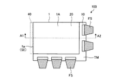
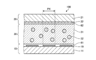
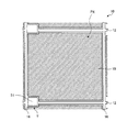
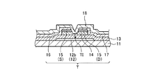
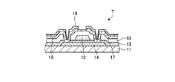
図1は、第一の実施形態に係る表示装置100の断面図である。図2は、表示装置100の平面図である。図1は、図2のA1−A2線に沿う断面図である。図3は、液晶層30の構成を示す断面図である。図4は、非散乱状態の液晶層30を示す断面図である。図5は、散乱状態の液晶層30を示す断面図である。図6は、表示装置100の一画素PXの模式的な平面図である。図7は、薄膜トランジスタTおよびその周辺の構造を示す平面図である。図8は、図7のA3−A4線に沿う断面図である。以下、液晶層30の層厚方向から見た状態を平面視といい、液晶層30の層厚方向と直交する方向から見た状態を断面視という。
図11は、第二の実施形態に係る表示装置200の断面図である。図12は、表示装置200の平面図である。図11は、図12のA5−A6線に沿う断面図である。本実施形態において第一の実施形態と共通する構成要素については、同じ符号を付し、詳細な説明は省略する。
図13は、第三の実施形態に係る表示装置300の断面図である。図14は、表示装置300の平面図である。図13は、図14のA7−A8線に沿う断面図である。本実施形態において第一の実施形態と共通する構成要素については、同じ符号を付し、詳細な説明は省略する。
図15および図16は、薄膜トランジスタTのバリエーションを示す断面図である。本実施形態において第一の実施形態と共通する構成要素については、同じ符号を付し、詳細な説明は省略する。
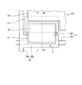
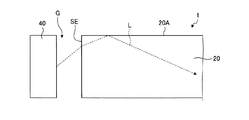
図18は、光源部40の配置のバリエーションを示す断面図である。
共通電極を有する第二の基板と、
前記第一の基板の前記薄膜トランジスタと重畳する位置に配置され、前記第一の基板から前記第二の基板に向けて突出した有機絶縁層と、
前記有機絶縁層の上面および側面を覆い、前記共通電極と電気的に接続された導電性の遮光層と、を有し、
前記有機絶縁層および前記遮光層は、前記第一の基板と前記第二の基板との間の間隙を保持する、表示装置。
前記遮光層は、前記光を反射する
(1)に記載の表示装置。
(1)または(2)に記載の表示装置。
(1)ないし(3)のいずれか1項に記載の表示装置。
(1)ないし(4)のいずれか一つに記載の表示装置。
前記第二の基板側から見て、前記遮光層は、前記ゲート線からはみ出さないように設けられている
(5)に記載の表示装置。
14 半導体層
19 画素電極
20 第二の基板
22 共通電極
30 液晶層
50 有機絶縁層
51 遮光層
100 表示装置
L 光
T 薄膜トランジスタ
Claims (6)
- 薄膜トランジスタを有する第一の基板と、
共通電極を有する第二の基板と、
前記第一の基板の前記薄膜トランジスタと重畳する位置に配置され、前記第一の基板から前記第二の基板に向けて突出した有機絶縁層と、
前記有機絶縁層の上面および側面を覆い、前記共通電極と電気的に接続された導電性の遮光層と、を有し、
前記有機絶縁層および前記遮光層は、前記第一の基板と前記第二の基板との間の間隙を保持する、表示装置。 - 前記第一の基板と前記第二の基板との間に配置され、前記第一の基板と前記第二の基板との間を反射しながら伝播する光を変調する液晶層を有し、
前記遮光層は、前記光を反射する
請求項1に記載の表示装置。 - 前記液晶層は、高分子分散型の液晶層である
請求項1または2に記載の表示装置。 - 前記有機絶縁層は、前記第一の基板と対向する底面が前記第二の基板と対向する上面よりも大きくなるようなテーパー形状を有する
請求項1ないし3のいずれか1項に記載の表示装置。 - 前記薄膜トランジスタは、ボトムゲート型の薄膜トランジスタである
請求項1ないし4のいずれか1項に記載の表示装置。 - 前記薄膜トランジスタと電気的に接続されたゲート線を有し、
前記第二の基板側から見て、前記遮光層は、前記ゲート線からはみ出さないように設けられている
請求項5に記載の表示装置。
Priority Applications (3)
| Application Number | Priority Date | Filing Date | Title |
|---|---|---|---|
| JP2016042808A JP2017156718A (ja) | 2016-03-04 | 2016-03-04 | 表示装置 |
| US15/440,180 US10067392B2 (en) | 2016-03-04 | 2017-02-23 | Display device |
| US16/045,268 US20180329265A1 (en) | 2016-03-04 | 2018-07-25 | Display device |
Applications Claiming Priority (1)
| Application Number | Priority Date | Filing Date | Title |
|---|---|---|---|
| JP2016042808A JP2017156718A (ja) | 2016-03-04 | 2016-03-04 | 表示装置 |
Publications (2)
| Publication Number | Publication Date |
|---|---|
| JP2017156718A true JP2017156718A (ja) | 2017-09-07 |
| JP2017156718A5 JP2017156718A5 (ja) | 2019-04-11 |
Family
ID=59722133
Family Applications (1)
| Application Number | Title | Priority Date | Filing Date |
|---|---|---|---|
| JP2016042808A Pending JP2017156718A (ja) | 2016-03-04 | 2016-03-04 | 表示装置 |
Country Status (2)
| Country | Link |
|---|---|
| US (2) | US10067392B2 (ja) |
| JP (1) | JP2017156718A (ja) |
Cited By (7)
| Publication number | Priority date | Publication date | Assignee | Title |
|---|---|---|---|---|
| JP2019053186A (ja) * | 2017-09-14 | 2019-04-04 | 株式会社ジャパンディスプレイ | 表示装置 |
| JP2019053097A (ja) * | 2017-09-12 | 2019-04-04 | 株式会社ジャパンディスプレイ | 表示装置 |
| JP2019066640A (ja) * | 2017-09-29 | 2019-04-25 | 株式会社ジャパンディスプレイ | 表示装置 |
| CN111221190A (zh) * | 2020-03-18 | 2020-06-02 | Tcl华星光电技术有限公司 | 显示装置 |
| JP2020086089A (ja) * | 2018-11-22 | 2020-06-04 | 株式会社ジャパンディスプレイ | 表示装置 |
| US11694647B2 (en) | 2018-12-11 | 2023-07-04 | Japan Display Inc. | Display device |
| JP7375238B2 (ja) | 2019-02-14 | 2023-11-07 | 株式会社ジャパンディスプレイ | 表示装置 |
Families Citing this family (5)
| Publication number | Priority date | Publication date | Assignee | Title |
|---|---|---|---|---|
| JP2017167214A (ja) | 2016-03-14 | 2017-09-21 | 株式会社ジャパンディスプレイ | 表示装置 |
| JP6720008B2 (ja) | 2016-07-22 | 2020-07-08 | 株式会社ジャパンディスプレイ | 表示装置および表示装置の駆動方法 |
| CN108051961B (zh) * | 2018-01-02 | 2021-05-07 | 京东方科技集团股份有限公司 | 一种液晶显示面板及其显示方法和液晶显示装置 |
| JP2019191230A (ja) | 2018-04-19 | 2019-10-31 | 株式会社ジャパンディスプレイ | 表示装置 |
| CN113287058A (zh) * | 2019-01-11 | 2021-08-20 | 株式会社日本显示器 | 显示装置 |
Family Cites Families (27)
| Publication number | Priority date | Publication date | Assignee | Title |
|---|---|---|---|---|
| TWI236556B (en) | 1996-10-16 | 2005-07-21 | Seiko Epson Corp | Substrate for a liquid crystal equipment, liquid crystal equipment and projection type display equipment |
| JP2001228454A (ja) | 2000-02-14 | 2001-08-24 | Toshiba Corp | 液晶表示装置及びそれを用いた投射型液晶表示装置 |
| JP2001337330A (ja) | 2000-05-26 | 2001-12-07 | Toshiba Corp | 液晶表示装置 |
| JP4299584B2 (ja) | 2003-05-23 | 2009-07-22 | Nec液晶テクノロジー株式会社 | 液晶表示装置 |
| JP2006220702A (ja) | 2005-02-08 | 2006-08-24 | Seiko Epson Corp | 液晶表示装置の製造方法、液晶表示装置および電子機器 |
| JP2007072114A (ja) | 2005-09-06 | 2007-03-22 | Sony Corp | 液晶表示素子およびその製造方法、並びに投射型表示装置 |
| CN100504543C (zh) * | 2007-03-06 | 2009-06-24 | 孙润光 | 显示装置以及含有该显示装置的手机、计算机和电视机 |
| JP5481790B2 (ja) | 2008-02-29 | 2014-04-23 | セイコーエプソン株式会社 | 電気光学装置 |
| JP2009223245A (ja) * | 2008-03-19 | 2009-10-01 | Hitachi Displays Ltd | 液晶表示装置 |
| JP5263593B2 (ja) | 2008-10-07 | 2013-08-14 | ソニー株式会社 | 照明装置および表示装置 |
| JP4752911B2 (ja) | 2008-12-26 | 2011-08-17 | ソニー株式会社 | 照明装置、表示装置、およびエッジライト方式のバックライトに用いる光変調素子の製造方法 |
| TWI408449B (zh) * | 2009-11-03 | 2013-09-11 | Wintek Corp | 液晶顯示面板 |
| JP5467389B2 (ja) | 2009-11-06 | 2014-04-09 | ソニー株式会社 | 照明装置および表示装置 |
| CN102640041A (zh) * | 2009-11-27 | 2012-08-15 | 株式会社半导体能源研究所 | 液晶显示装置 |
| KR101840623B1 (ko) * | 2009-12-04 | 2018-03-21 | 가부시키가이샤 한도오따이 에네루기 켄큐쇼 | 표시 장치 및 이를 포함하는 전자 기기 |
| JP5756931B2 (ja) | 2009-12-11 | 2015-07-29 | ソニー株式会社 | 照明装置および表示装置 |
| JP5467388B2 (ja) | 2010-04-06 | 2014-04-09 | ソニー株式会社 | 照明装置および表示装置 |
| JP2012088486A (ja) | 2010-10-19 | 2012-05-10 | Sony Corp | 表示パネルおよび表示装置 |
| JP5699786B2 (ja) | 2011-04-28 | 2015-04-15 | ソニー株式会社 | 表示装置および照明装置 |
| JP6014308B2 (ja) | 2011-06-08 | 2016-10-25 | 株式会社ジャパンディスプレイ | 表示装置 |
| TW201400946A (zh) | 2012-05-09 | 2014-01-01 | Sony Corp | 照明裝置及顯示裝置 |
| TWI545377B (zh) * | 2012-05-11 | 2016-08-11 | Sony Corp | Lighting device and display device |
| JP2015044795A (ja) * | 2013-07-31 | 2015-03-12 | 株式会社半導体エネルギー研究所 | トリフルオロフェニル誘導体、液晶組成物及び液晶表示装置 |
| KR102130545B1 (ko) * | 2013-11-27 | 2020-07-07 | 삼성디스플레이 주식회사 | 액정 표시 장치 |
| TWI599818B (zh) | 2014-10-22 | 2017-09-21 | 日本顯示器股份有限公司 | 顯示裝置 |
| JP6364335B2 (ja) | 2014-12-04 | 2018-07-25 | 株式会社ジャパンディスプレイ | 表示装置 |
| JP2017032782A (ja) | 2015-07-31 | 2017-02-09 | 株式会社ジャパンディスプレイ | 表示装置 |
-
2016
- 2016-03-04 JP JP2016042808A patent/JP2017156718A/ja active Pending
-
2017
- 2017-02-23 US US15/440,180 patent/US10067392B2/en active Active
-
2018
- 2018-07-25 US US16/045,268 patent/US20180329265A1/en not_active Abandoned
Cited By (11)
| Publication number | Priority date | Publication date | Assignee | Title |
|---|---|---|---|---|
| JP2019053097A (ja) * | 2017-09-12 | 2019-04-04 | 株式会社ジャパンディスプレイ | 表示装置 |
| JP7043204B2 (ja) | 2017-09-12 | 2022-03-29 | 株式会社ジャパンディスプレイ | 表示装置 |
| JP2019053186A (ja) * | 2017-09-14 | 2019-04-04 | 株式会社ジャパンディスプレイ | 表示装置 |
| JP7005243B2 (ja) | 2017-09-14 | 2022-01-21 | 株式会社ジャパンディスプレイ | 表示装置 |
| JP2019066640A (ja) * | 2017-09-29 | 2019-04-25 | 株式会社ジャパンディスプレイ | 表示装置 |
| JP7030468B2 (ja) | 2017-09-29 | 2022-03-07 | 株式会社ジャパンディスプレイ | 表示装置 |
| JP2020086089A (ja) * | 2018-11-22 | 2020-06-04 | 株式会社ジャパンディスプレイ | 表示装置 |
| JP7160334B2 (ja) | 2018-11-22 | 2022-10-25 | 株式会社ジャパンディスプレイ | 表示装置 |
| US11694647B2 (en) | 2018-12-11 | 2023-07-04 | Japan Display Inc. | Display device |
| JP7375238B2 (ja) | 2019-02-14 | 2023-11-07 | 株式会社ジャパンディスプレイ | 表示装置 |
| CN111221190A (zh) * | 2020-03-18 | 2020-06-02 | Tcl华星光电技术有限公司 | 显示装置 |
Also Published As
| Publication number | Publication date |
|---|---|
| US20170255072A1 (en) | 2017-09-07 |
| US10067392B2 (en) | 2018-09-04 |
| US20180329265A1 (en) | 2018-11-15 |
Similar Documents
| Publication | Publication Date | Title |
|---|---|---|
| JP2017156718A (ja) | 表示装置 | |
| US10782558B2 (en) | Display device | |
| US20230359087A1 (en) | Display device | |
| US10877306B2 (en) | Display device | |
| US9454032B2 (en) | Display device | |
| JP2017167527A (ja) | 表示装置 | |
| JP6460148B2 (ja) | 電気光学装置および電子機器 | |
| KR102614676B1 (ko) | 액정 표시 장치 | |
| JP2019148683A (ja) | 電気光学装置および電子機器 | |
| JP7083675B2 (ja) | 表示装置 | |
| JP2022053996A (ja) | 電気光学装置および電子機器 | |
| US11754892B2 (en) | Electro-optical device and electronic apparatus | |
| KR102589859B1 (ko) | 색필터 표시판 및 이를 포함하는 표시 장치 | |
| US11003010B2 (en) | Optical waveguide display substrate, and display device | |
| JP2007322766A (ja) | 液晶表示装置及び電子機器 | |
| JP7218467B2 (ja) | 表示装置 | |
| US11624960B2 (en) | Electro-optical device and electronic apparatus | |
| CN114253022B (zh) | 显示装置 | |
| US11614668B2 (en) | Display device | |
| JP5009114B2 (ja) | 液晶表示装置及び電子機器 | |
| JP2020027191A (ja) | 表示装置 | |
| JP2012118297A (ja) | 表示パネルおよびその製造方法、表示装置、ならびに電子機器 | |
| JP2016224305A (ja) | 液晶表示装置 | |
| JP2005338500A (ja) | 液晶表示素子及び液晶表示装置 |
Legal Events
| Date | Code | Title | Description |
|---|---|---|---|
| A521 | Written amendment |
Free format text: JAPANESE INTERMEDIATE CODE: A523 Effective date: 20190227 |
|
| A621 | Written request for application examination |
Free format text: JAPANESE INTERMEDIATE CODE: A621 Effective date: 20190227 |
|
| A977 | Report on retrieval |
Free format text: JAPANESE INTERMEDIATE CODE: A971007 Effective date: 20200128 |
|
| A131 | Notification of reasons for refusal |
Free format text: JAPANESE INTERMEDIATE CODE: A131 Effective date: 20200204 |
|
| A02 | Decision of refusal |
Free format text: JAPANESE INTERMEDIATE CODE: A02 Effective date: 20200728 |