JP2017143096A - Wiring board, semiconductor device and wiring board manufacturing method - Google Patents
Wiring board, semiconductor device and wiring board manufacturing method Download PDFInfo
- Publication number
- JP2017143096A JP2017143096A JP2016021698A JP2016021698A JP2017143096A JP 2017143096 A JP2017143096 A JP 2017143096A JP 2016021698 A JP2016021698 A JP 2016021698A JP 2016021698 A JP2016021698 A JP 2016021698A JP 2017143096 A JP2017143096 A JP 2017143096A
- Authority
- JP
- Japan
- Prior art keywords
- opening
- hole
- holes
- core substrate
- wiring board
- Prior art date
- Legal status (The legal status is an assumption and is not a legal conclusion. Google has not performed a legal analysis and makes no representation as to the accuracy of the status listed.)
- Granted
Links
Images


Classifications
-
- H—ELECTRICITY
- H01—ELECTRIC ELEMENTS
- H01L—SEMICONDUCTOR DEVICES NOT COVERED BY CLASS H10
- H01L25/00—Assemblies consisting of a plurality of individual semiconductor or other solid state devices ; Multistep manufacturing processes thereof
- H01L25/03—Assemblies consisting of a plurality of individual semiconductor or other solid state devices ; Multistep manufacturing processes thereof all the devices being of a type provided for in the same subgroup of groups H01L27/00 - H01L33/00, or in a single subclass of H10K, H10N, e.g. assemblies of rectifier diodes
- H01L25/10—Assemblies consisting of a plurality of individual semiconductor or other solid state devices ; Multistep manufacturing processes thereof all the devices being of a type provided for in the same subgroup of groups H01L27/00 - H01L33/00, or in a single subclass of H10K, H10N, e.g. assemblies of rectifier diodes the devices having separate containers
- H01L25/11—Assemblies consisting of a plurality of individual semiconductor or other solid state devices ; Multistep manufacturing processes thereof all the devices being of a type provided for in the same subgroup of groups H01L27/00 - H01L33/00, or in a single subclass of H10K, H10N, e.g. assemblies of rectifier diodes the devices having separate containers the devices being of a type provided for in group H01L29/00
- H01L25/117—Stacked arrangements of devices
-
- H—ELECTRICITY
- H01—ELECTRIC ELEMENTS
- H01L—SEMICONDUCTOR DEVICES NOT COVERED BY CLASS H10
- H01L21/00—Processes or apparatus adapted for the manufacture or treatment of semiconductor or solid state devices or of parts thereof
- H01L21/02—Manufacture or treatment of semiconductor devices or of parts thereof
- H01L21/04—Manufacture or treatment of semiconductor devices or of parts thereof the devices having at least one potential-jump barrier or surface barrier, e.g. PN junction, depletion layer or carrier concentration layer
- H01L21/50—Assembly of semiconductor devices using processes or apparatus not provided for in a single one of the subgroups H01L21/06 - H01L21/326, e.g. sealing of a cap to a base of a container
- H01L21/56—Encapsulations, e.g. encapsulation layers, coatings
- H01L21/563—Encapsulation of active face of flip-chip device, e.g. underfilling or underencapsulation of flip-chip, encapsulation preform on chip or mounting substrate
-
- H—ELECTRICITY
- H01—ELECTRIC ELEMENTS
- H01L—SEMICONDUCTOR DEVICES NOT COVERED BY CLASS H10
- H01L23/00—Details of semiconductor or other solid state devices
- H01L23/28—Encapsulations, e.g. encapsulating layers, coatings, e.g. for protection
- H01L23/31—Encapsulations, e.g. encapsulating layers, coatings, e.g. for protection characterised by the arrangement or shape
- H01L23/3107—Encapsulations, e.g. encapsulating layers, coatings, e.g. for protection characterised by the arrangement or shape the device being completely enclosed
- H01L23/3121—Encapsulations, e.g. encapsulating layers, coatings, e.g. for protection characterised by the arrangement or shape the device being completely enclosed a substrate forming part of the encapsulation
- H01L23/3128—Encapsulations, e.g. encapsulating layers, coatings, e.g. for protection characterised by the arrangement or shape the device being completely enclosed a substrate forming part of the encapsulation the substrate having spherical bumps for external connection
-
- H—ELECTRICITY
- H01—ELECTRIC ELEMENTS
- H01L—SEMICONDUCTOR DEVICES NOT COVERED BY CLASS H10
- H01L23/00—Details of semiconductor or other solid state devices
- H01L23/48—Arrangements for conducting electric current to or from the solid state body in operation, e.g. leads, terminal arrangements ; Selection of materials therefor
- H01L23/488—Arrangements for conducting electric current to or from the solid state body in operation, e.g. leads, terminal arrangements ; Selection of materials therefor consisting of soldered or bonded constructions
- H01L23/498—Leads, i.e. metallisations or lead-frames on insulating substrates, e.g. chip carriers
- H01L23/49822—Multilayer substrates
-
- H—ELECTRICITY
- H01—ELECTRIC ELEMENTS
- H01L—SEMICONDUCTOR DEVICES NOT COVERED BY CLASS H10
- H01L23/00—Details of semiconductor or other solid state devices
- H01L23/48—Arrangements for conducting electric current to or from the solid state body in operation, e.g. leads, terminal arrangements ; Selection of materials therefor
- H01L23/488—Arrangements for conducting electric current to or from the solid state body in operation, e.g. leads, terminal arrangements ; Selection of materials therefor consisting of soldered or bonded constructions
- H01L23/498—Leads, i.e. metallisations or lead-frames on insulating substrates, e.g. chip carriers
- H01L23/49827—Via connections through the substrates, e.g. pins going through the substrate, coaxial cables
-
- H—ELECTRICITY
- H01—ELECTRIC ELEMENTS
- H01L—SEMICONDUCTOR DEVICES NOT COVERED BY CLASS H10
- H01L23/00—Details of semiconductor or other solid state devices
- H01L23/52—Arrangements for conducting electric current within the device in operation from one component to another, i.e. interconnections, e.g. wires, lead frames
- H01L23/538—Arrangements for conducting electric current within the device in operation from one component to another, i.e. interconnections, e.g. wires, lead frames the interconnection structure between a plurality of semiconductor chips being formed on, or in, insulating substrates
- H01L23/5389—Arrangements for conducting electric current within the device in operation from one component to another, i.e. interconnections, e.g. wires, lead frames the interconnection structure between a plurality of semiconductor chips being formed on, or in, insulating substrates the chips being integrally enclosed by the interconnect and support structures
-
- H—ELECTRICITY
- H01—ELECTRIC ELEMENTS
- H01L—SEMICONDUCTOR DEVICES NOT COVERED BY CLASS H10
- H01L24/00—Arrangements for connecting or disconnecting semiconductor or solid-state bodies; Methods or apparatus related thereto
- H01L24/01—Means for bonding being attached to, or being formed on, the surface to be connected, e.g. chip-to-package, die-attach, "first-level" interconnects; Manufacturing methods related thereto
- H01L24/02—Bonding areas ; Manufacturing methods related thereto
- H01L24/07—Structure, shape, material or disposition of the bonding areas after the connecting process
- H01L24/09—Structure, shape, material or disposition of the bonding areas after the connecting process of a plurality of bonding areas
-
- H—ELECTRICITY
- H01—ELECTRIC ELEMENTS
- H01L—SEMICONDUCTOR DEVICES NOT COVERED BY CLASS H10
- H01L24/00—Arrangements for connecting or disconnecting semiconductor or solid-state bodies; Methods or apparatus related thereto
- H01L24/01—Means for bonding being attached to, or being formed on, the surface to be connected, e.g. chip-to-package, die-attach, "first-level" interconnects; Manufacturing methods related thereto
- H01L24/10—Bump connectors ; Manufacturing methods related thereto
- H01L24/15—Structure, shape, material or disposition of the bump connectors after the connecting process
- H01L24/17—Structure, shape, material or disposition of the bump connectors after the connecting process of a plurality of bump connectors
-
- H—ELECTRICITY
- H01—ELECTRIC ELEMENTS
- H01L—SEMICONDUCTOR DEVICES NOT COVERED BY CLASS H10
- H01L24/00—Arrangements for connecting or disconnecting semiconductor or solid-state bodies; Methods or apparatus related thereto
- H01L24/01—Means for bonding being attached to, or being formed on, the surface to be connected, e.g. chip-to-package, die-attach, "first-level" interconnects; Manufacturing methods related thereto
- H01L24/18—High density interconnect [HDI] connectors; Manufacturing methods related thereto
- H01L24/19—Manufacturing methods of high density interconnect preforms
-
- H—ELECTRICITY
- H01—ELECTRIC ELEMENTS
- H01L—SEMICONDUCTOR DEVICES NOT COVERED BY CLASS H10
- H01L24/00—Arrangements for connecting or disconnecting semiconductor or solid-state bodies; Methods or apparatus related thereto
- H01L24/01—Means for bonding being attached to, or being formed on, the surface to be connected, e.g. chip-to-package, die-attach, "first-level" interconnects; Manufacturing methods related thereto
- H01L24/18—High density interconnect [HDI] connectors; Manufacturing methods related thereto
- H01L24/20—Structure, shape, material or disposition of high density interconnect preforms
-
- H—ELECTRICITY
- H01—ELECTRIC ELEMENTS
- H01L—SEMICONDUCTOR DEVICES NOT COVERED BY CLASS H10
- H01L24/00—Arrangements for connecting or disconnecting semiconductor or solid-state bodies; Methods or apparatus related thereto
- H01L24/01—Means for bonding being attached to, or being formed on, the surface to be connected, e.g. chip-to-package, die-attach, "first-level" interconnects; Manufacturing methods related thereto
- H01L24/18—High density interconnect [HDI] connectors; Manufacturing methods related thereto
- H01L24/23—Structure, shape, material or disposition of the high density interconnect connectors after the connecting process
- H01L24/25—Structure, shape, material or disposition of the high density interconnect connectors after the connecting process of a plurality of high density interconnect connectors
-
- H—ELECTRICITY
- H01—ELECTRIC ELEMENTS
- H01L—SEMICONDUCTOR DEVICES NOT COVERED BY CLASS H10
- H01L24/00—Arrangements for connecting or disconnecting semiconductor or solid-state bodies; Methods or apparatus related thereto
- H01L24/93—Batch processes
- H01L24/95—Batch processes at chip-level, i.e. with connecting carried out on a plurality of singulated devices, i.e. on diced chips
- H01L24/96—Batch processes at chip-level, i.e. with connecting carried out on a plurality of singulated devices, i.e. on diced chips the devices being encapsulated in a common layer, e.g. neo-wafer or pseudo-wafer, said common layer being separable into individual assemblies after connecting
-
- H—ELECTRICITY
- H01—ELECTRIC ELEMENTS
- H01L—SEMICONDUCTOR DEVICES NOT COVERED BY CLASS H10
- H01L21/00—Processes or apparatus adapted for the manufacture or treatment of semiconductor or solid state devices or of parts thereof
- H01L21/02—Manufacture or treatment of semiconductor devices or of parts thereof
- H01L21/04—Manufacture or treatment of semiconductor devices or of parts thereof the devices having at least one potential-jump barrier or surface barrier, e.g. PN junction, depletion layer or carrier concentration layer
- H01L21/50—Assembly of semiconductor devices using processes or apparatus not provided for in a single one of the subgroups H01L21/06 - H01L21/326, e.g. sealing of a cap to a base of a container
- H01L21/56—Encapsulations, e.g. encapsulation layers, coatings
- H01L21/568—Temporary substrate used as encapsulation process aid
-
- H—ELECTRICITY
- H01—ELECTRIC ELEMENTS
- H01L—SEMICONDUCTOR DEVICES NOT COVERED BY CLASS H10
- H01L2224/00—Indexing scheme for arrangements for connecting or disconnecting semiconductor or solid-state bodies and methods related thereto as covered by H01L24/00
- H01L2224/01—Means for bonding being attached to, or being formed on, the surface to be connected, e.g. chip-to-package, die-attach, "first-level" interconnects; Manufacturing methods related thereto
- H01L2224/02—Bonding areas; Manufacturing methods related thereto
- H01L2224/04—Structure, shape, material or disposition of the bonding areas prior to the connecting process
- H01L2224/0401—Bonding areas specifically adapted for bump connectors, e.g. under bump metallisation [UBM]
-
- H—ELECTRICITY
- H01—ELECTRIC ELEMENTS
- H01L—SEMICONDUCTOR DEVICES NOT COVERED BY CLASS H10
- H01L2224/00—Indexing scheme for arrangements for connecting or disconnecting semiconductor or solid-state bodies and methods related thereto as covered by H01L24/00
- H01L2224/01—Means for bonding being attached to, or being formed on, the surface to be connected, e.g. chip-to-package, die-attach, "first-level" interconnects; Manufacturing methods related thereto
- H01L2224/02—Bonding areas; Manufacturing methods related thereto
- H01L2224/04—Structure, shape, material or disposition of the bonding areas prior to the connecting process
- H01L2224/04105—Bonding areas formed on an encapsulation of the semiconductor or solid-state body, e.g. bonding areas on chip-scale packages
-
- H—ELECTRICITY
- H01—ELECTRIC ELEMENTS
- H01L—SEMICONDUCTOR DEVICES NOT COVERED BY CLASS H10
- H01L2224/00—Indexing scheme for arrangements for connecting or disconnecting semiconductor or solid-state bodies and methods related thereto as covered by H01L24/00
- H01L2224/01—Means for bonding being attached to, or being formed on, the surface to be connected, e.g. chip-to-package, die-attach, "first-level" interconnects; Manufacturing methods related thereto
- H01L2224/10—Bump connectors; Manufacturing methods related thereto
- H01L2224/12—Structure, shape, material or disposition of the bump connectors prior to the connecting process
- H01L2224/12105—Bump connectors formed on an encapsulation of the semiconductor or solid-state body, e.g. bumps on chip-scale packages
-
- H—ELECTRICITY
- H01—ELECTRIC ELEMENTS
- H01L—SEMICONDUCTOR DEVICES NOT COVERED BY CLASS H10
- H01L2224/00—Indexing scheme for arrangements for connecting or disconnecting semiconductor or solid-state bodies and methods related thereto as covered by H01L24/00
- H01L2224/01—Means for bonding being attached to, or being formed on, the surface to be connected, e.g. chip-to-package, die-attach, "first-level" interconnects; Manufacturing methods related thereto
- H01L2224/10—Bump connectors; Manufacturing methods related thereto
- H01L2224/15—Structure, shape, material or disposition of the bump connectors after the connecting process
- H01L2224/16—Structure, shape, material or disposition of the bump connectors after the connecting process of an individual bump connector
- H01L2224/161—Disposition
- H01L2224/16151—Disposition the bump connector connecting between a semiconductor or solid-state body and an item not being a semiconductor or solid-state body, e.g. chip-to-substrate, chip-to-passive
- H01L2224/16221—Disposition the bump connector connecting between a semiconductor or solid-state body and an item not being a semiconductor or solid-state body, e.g. chip-to-substrate, chip-to-passive the body and the item being stacked
- H01L2224/16225—Disposition the bump connector connecting between a semiconductor or solid-state body and an item not being a semiconductor or solid-state body, e.g. chip-to-substrate, chip-to-passive the body and the item being stacked the item being non-metallic, e.g. insulating substrate with or without metallisation
- H01L2224/16227—Disposition the bump connector connecting between a semiconductor or solid-state body and an item not being a semiconductor or solid-state body, e.g. chip-to-substrate, chip-to-passive the body and the item being stacked the item being non-metallic, e.g. insulating substrate with or without metallisation the bump connector connecting to a bond pad of the item
-
- H—ELECTRICITY
- H01—ELECTRIC ELEMENTS
- H01L—SEMICONDUCTOR DEVICES NOT COVERED BY CLASS H10
- H01L2224/00—Indexing scheme for arrangements for connecting or disconnecting semiconductor or solid-state bodies and methods related thereto as covered by H01L24/00
- H01L2224/01—Means for bonding being attached to, or being formed on, the surface to be connected, e.g. chip-to-package, die-attach, "first-level" interconnects; Manufacturing methods related thereto
- H01L2224/18—High density interconnect [HDI] connectors; Manufacturing methods related thereto
- H01L2224/23—Structure, shape, material or disposition of the high density interconnect connectors after the connecting process
- H01L2224/25—Structure, shape, material or disposition of the high density interconnect connectors after the connecting process of a plurality of high density interconnect connectors
- H01L2224/251—Disposition
- H01L2224/2518—Disposition being disposed on at least two different sides of the body, e.g. dual array
-
- H—ELECTRICITY
- H01—ELECTRIC ELEMENTS
- H01L—SEMICONDUCTOR DEVICES NOT COVERED BY CLASS H10
- H01L2224/00—Indexing scheme for arrangements for connecting or disconnecting semiconductor or solid-state bodies and methods related thereto as covered by H01L24/00
- H01L2224/01—Means for bonding being attached to, or being formed on, the surface to be connected, e.g. chip-to-package, die-attach, "first-level" interconnects; Manufacturing methods related thereto
- H01L2224/26—Layer connectors, e.g. plate connectors, solder or adhesive layers; Manufacturing methods related thereto
- H01L2224/31—Structure, shape, material or disposition of the layer connectors after the connecting process
- H01L2224/32—Structure, shape, material or disposition of the layer connectors after the connecting process of an individual layer connector
- H01L2224/321—Disposition
- H01L2224/32151—Disposition the layer connector connecting between a semiconductor or solid-state body and an item not being a semiconductor or solid-state body, e.g. chip-to-substrate, chip-to-passive
- H01L2224/32221—Disposition the layer connector connecting between a semiconductor or solid-state body and an item not being a semiconductor or solid-state body, e.g. chip-to-substrate, chip-to-passive the body and the item being stacked
- H01L2224/32225—Disposition the layer connector connecting between a semiconductor or solid-state body and an item not being a semiconductor or solid-state body, e.g. chip-to-substrate, chip-to-passive the body and the item being stacked the item being non-metallic, e.g. insulating substrate with or without metallisation
-
- H—ELECTRICITY
- H01—ELECTRIC ELEMENTS
- H01L—SEMICONDUCTOR DEVICES NOT COVERED BY CLASS H10
- H01L2224/00—Indexing scheme for arrangements for connecting or disconnecting semiconductor or solid-state bodies and methods related thereto as covered by H01L24/00
- H01L2224/73—Means for bonding being of different types provided for in two or more of groups H01L2224/10, H01L2224/18, H01L2224/26, H01L2224/34, H01L2224/42, H01L2224/50, H01L2224/63, H01L2224/71
- H01L2224/732—Location after the connecting process
- H01L2224/73201—Location after the connecting process on the same surface
- H01L2224/73203—Bump and layer connectors
- H01L2224/73204—Bump and layer connectors the bump connector being embedded into the layer connector
-
- H—ELECTRICITY
- H01—ELECTRIC ELEMENTS
- H01L—SEMICONDUCTOR DEVICES NOT COVERED BY CLASS H10
- H01L2224/00—Indexing scheme for arrangements for connecting or disconnecting semiconductor or solid-state bodies and methods related thereto as covered by H01L24/00
- H01L2224/91—Methods for connecting semiconductor or solid state bodies including different methods provided for in two or more of groups H01L2224/80 - H01L2224/90
- H01L2224/92—Specific sequence of method steps
- H01L2224/921—Connecting a surface with connectors of different types
- H01L2224/9212—Sequential connecting processes
- H01L2224/92122—Sequential connecting processes the first connecting process involving a bump connector
- H01L2224/92125—Sequential connecting processes the first connecting process involving a bump connector the second connecting process involving a layer connector
-
- H—ELECTRICITY
- H01—ELECTRIC ELEMENTS
- H01L—SEMICONDUCTOR DEVICES NOT COVERED BY CLASS H10
- H01L2225/00—Details relating to assemblies covered by the group H01L25/00 but not provided for in its subgroups
- H01L2225/03—All the devices being of a type provided for in the same subgroup of groups H01L27/00 - H01L33/648 and H10K99/00
- H01L2225/10—All the devices being of a type provided for in the same subgroup of groups H01L27/00 - H01L33/648 and H10K99/00 the devices having separate containers
- H01L2225/1005—All the devices being of a type provided for in the same subgroup of groups H01L27/00 - H01L33/648 and H10K99/00 the devices having separate containers the devices being of a type provided for in group H01L27/00
- H01L2225/1011—All the devices being of a type provided for in the same subgroup of groups H01L27/00 - H01L33/648 and H10K99/00 the devices having separate containers the devices being of a type provided for in group H01L27/00 the containers being in a stacked arrangement
- H01L2225/1017—All the devices being of a type provided for in the same subgroup of groups H01L27/00 - H01L33/648 and H10K99/00 the devices having separate containers the devices being of a type provided for in group H01L27/00 the containers being in a stacked arrangement the lowermost container comprising a device support
- H01L2225/1035—All the devices being of a type provided for in the same subgroup of groups H01L27/00 - H01L33/648 and H10K99/00 the devices having separate containers the devices being of a type provided for in group H01L27/00 the containers being in a stacked arrangement the lowermost container comprising a device support the device being entirely enclosed by the support, e.g. high-density interconnect [HDI]
-
- H—ELECTRICITY
- H01—ELECTRIC ELEMENTS
- H01L—SEMICONDUCTOR DEVICES NOT COVERED BY CLASS H10
- H01L23/00—Details of semiconductor or other solid state devices
- H01L23/12—Mountings, e.g. non-detachable insulating substrates
- H01L23/13—Mountings, e.g. non-detachable insulating substrates characterised by the shape
-
- H—ELECTRICITY
- H01—ELECTRIC ELEMENTS
- H01L—SEMICONDUCTOR DEVICES NOT COVERED BY CLASS H10
- H01L23/00—Details of semiconductor or other solid state devices
- H01L23/48—Arrangements for conducting electric current to or from the solid state body in operation, e.g. leads, terminal arrangements ; Selection of materials therefor
- H01L23/488—Arrangements for conducting electric current to or from the solid state body in operation, e.g. leads, terminal arrangements ; Selection of materials therefor consisting of soldered or bonded constructions
- H01L23/498—Leads, i.e. metallisations or lead-frames on insulating substrates, e.g. chip carriers
- H01L23/49811—Additional leads joined to the metallisation on the insulating substrate, e.g. pins, bumps, wires, flat leads
- H01L23/49816—Spherical bumps on the substrate for external connection, e.g. ball grid arrays [BGA]
-
- H—ELECTRICITY
- H01—ELECTRIC ELEMENTS
- H01L—SEMICONDUCTOR DEVICES NOT COVERED BY CLASS H10
- H01L2924/00—Indexing scheme for arrangements or methods for connecting or disconnecting semiconductor or solid-state bodies as covered by H01L24/00
- H01L2924/15—Details of package parts other than the semiconductor or other solid state devices to be connected
- H01L2924/151—Die mounting substrate
- H01L2924/153—Connection portion
- H01L2924/1531—Connection portion the connection portion being formed only on the surface of the substrate opposite to the die mounting surface
- H01L2924/15311—Connection portion the connection portion being formed only on the surface of the substrate opposite to the die mounting surface being a ball array, e.g. BGA
Abstract
Description
本発明は、配線基板、半導体装置及び配線基板の製造方法に関するものである。 The present invention relates to a wiring board, a semiconductor device, and a manufacturing method of the wiring board.
従来、電子部品を内蔵した配線基板が知られている(例えば、特許文献1参照)。電子部品は、配線基板のコア基板に形成された開口部内に配置されている。このような配線基板は、次のような工程により得られる。まず、電子部品より大きな開口部が形成されたコア基板の片面に、開口部を塞ぐように仮止めテープを貼付する。次に、開口部内に電子部品を配置した後、開口部内に絶縁樹脂を充填する。そして、仮止めテープを剥離し、その仮止めテープが貼付されていた面に絶縁樹脂をラミネートする。このとき、図11(a)に示すような構造体が得られる。この構造体では、コア基板201の開口部202に電子部品203が配置され、その電子部品203を被覆する絶縁樹脂204が、開口部202内に充填されるとともにコア基板201の上下両面に形成されている。このときの絶縁樹脂204は半硬化状態である。次に、図11(b)に示すように、半硬化状態の絶縁樹脂204を150〜180℃程度の温度雰囲気で熱硬化処理を行うことにより硬化させる。この熱硬化処理では、コア基板201と電子部品203との双方が高温により膨張し(図中矢印参照)、絶縁樹脂204の硬化によって各材料の位置が固定される。続いて、図11(c)に示す工程では、図11(b)に示した構造体が冷却される。その後、絶縁樹脂204の上下両面に所定数の絶縁層と配線層を積層する。
Conventionally, a wiring board having a built-in electronic component is known (see, for example, Patent Document 1). The electronic component is disposed in an opening formed in the core substrate of the wiring substrate. Such a wiring board is obtained by the following process. First, a temporary fixing tape is affixed to one side of the core substrate having an opening larger than the electronic component so as to close the opening. Next, after an electronic component is disposed in the opening, an insulating resin is filled in the opening. Then, the temporary fixing tape is peeled off, and an insulating resin is laminated on the surface on which the temporary fixing tape has been applied. At this time, a structure as shown in FIG. In this structure, the
ところで、コア基板201の熱膨張率(CTE:Coefficient of Thermal Expansion)よりも電子部品203の熱膨張率が低いと、上記の冷却時に、電子部品203よりもコア基板201の収縮が大きくなる。このため、電子部品203に圧縮応力がかかる(図11(c)の矢印参照)。この圧縮応力が大きくなると、図11(d)に示すように、圧縮応力に耐えられず、電子部品203周辺が座屈変形し、電子部品203周辺が片面側に突出する。この場合には、絶縁樹脂204上に配線を形成することが困難になる。
By the way, when the thermal expansion coefficient of the
これに対し、電子部品203と開口部202の内面との隙間を広く確保し、その隙間に絶縁樹脂204を充填することにより、上記の冷却時に電子部品203にかかる圧縮応力を緩和することができる。しかし、開口部202が大きくなると、その開口部202内に絶縁樹脂204を十分に充填することができずに、開口部202の上部に形成された絶縁樹脂204に窪みが形成される場合がある。すると、その絶縁樹脂204上に配線層を形成する際に支障が生じる。
On the other hand, by ensuring a wide gap between the
本発明の一観点によれば、コア基板と、前記コア基板の第1面と該第1面と反対側の第2面との間を貫通し、平面形状が矩形状に形成された開口部と、前記コア基板の第1面と第2面との間を貫通し、前記開口部と離間して形成された複数の第1貫通孔と、前記開口部内に配置された電子部品と、前記第1貫通孔に充填された第1絶縁材と、前記開口部の内面と前記電子部品との間に充填された第2絶縁材と、を有し、前記第1貫通孔は、平面視において、前記開口部の角部の周囲に、前記角部を構成する前記開口部の2つの辺に沿ってL字形に連続して形成されている。 According to one aspect of the present invention, an opening having a rectangular planar shape penetrating between a core substrate and a first surface of the core substrate and a second surface opposite to the first surface. A plurality of first through holes formed between the first surface and the second surface of the core substrate and spaced apart from the opening, and the electronic components disposed in the opening, A first insulating material filled in the first through-hole, and a second insulating material filled between the inner surface of the opening and the electronic component, the first through-hole in plan view , Around the corner of the opening, and continuously formed in an L shape along the two sides of the opening constituting the corner.
本発明の一観点によれば、配線形成性を向上できるという効果を奏する。 According to one aspect of the present invention, there is an effect that the wiring formability can be improved.
以下、一実施形態について添付図面を参照して説明する。
なお、添付図面は、部分的に拡大して示している場合があり、寸法、比率などは実際と異なる場合がある。また、断面図では、各部材の断面構造を分かりやすくするために、一部のハッチングを省略している。
Hereinafter, an embodiment will be described with reference to the accompanying drawings.
Note that the attached drawings may be partially enlarged, and dimensions and ratios may differ from actual ones. In the cross-sectional view, some hatchings are omitted for easy understanding of the cross-sectional structure of each member.
図1に示すように、配線基板20はコア部21を有している。コア部21は、コア基板31と、コア基板31の第1面31A(図1では、上面)に形成された配線層41と、コア基板31の第2面31B(図1では、下面)に形成された配線層42とを有している。コア基板31は、例えば補強材であるガラスクロス(ガラス織布)にエポキシ樹脂を主成分とする熱硬化性の絶縁性樹脂を含浸させ硬化させた、いわゆるガラスエポキシ基板である。なお、補強材として、ガラスやアラミドの織布や不織布、液晶ポリマ(LCP:Liquid Crystal Polymer)織布やLCP不織布を用いることができる。また、絶縁性樹脂として、エポキシ樹脂に限らず、ポリイミド樹脂やシアネート樹脂を用いることができる。
As shown in FIG. 1, the
コア基板31は、所定位置に形成された貫通孔32を有している。貫通孔32は、コア基板31の第1面31Aと第2面31Bとの間、つまり厚さ方向に貫通するように形成されている。貫通孔32内には、コア基板31の第1面31Aと第2面31Bとの間を貫通する貫通電極33が形成されている。貫通電極33の材料は、例えば銅や銅合金である。
The
コア基板31は、所定の位置に開口部34を有している。開口部34は、コア基板31の第1面31Aと第2面31Bとの間を貫通するように形成されている。開口部34は、図1において下側(コア基板31の第2面31B側)から上側(コア基板31の第1面31A側)に向かうに連れて開口幅が小さくなるテーパ状に形成されている。
The
コア基板31は、開口部34の周囲に、互いに離間して形成された複数の貫通孔35を有している。各貫通孔35は、開口部34と離間して形成されている。各貫通孔35は、例えば貫通孔32よりも開口部34側の領域に形成されている。各貫通孔35は、コア基板31の第1面31Aと第2面31Bとの間を貫通するように形成されている。各貫通孔35は、開口部34と同様に、図1において下側(第2面31B側)から上側(第1面31A側)に向かうに連れて開口幅が小さくなるテーパ状に形成されている。
The
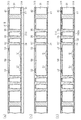
図2(a)に示すように、開口部34の平面形状は、例えば矩形状に形成されている。なお、本明細書における「矩形状」とは、厳密に矩形である場合のみならず、矩形の角部が面取りされた形状や、部分的に凹部や凸部が形成されているものも含むものとする。
As shown in FIG. 2A, the planar shape of the
貫通孔35は、開口部34の外周縁(開口縁)を囲む配置で複数列(ここでは、三列)に設けられている。以下の説明では、便宜上、三列の貫通孔35を、開口部34の外周縁側から順に、「1列目の貫通孔35」、「2列目の貫通孔35」、「3列目の貫通孔35」と称する。
The through holes 35 are provided in a plurality of rows (here, three rows) so as to surround the outer peripheral edge (opening edge) of the
1,2列目の複数の貫通孔35は、開口部34の外周縁を全周に亘って囲むように配置されている。1列目の貫通孔35と2列目の貫通孔35とは互いに離間して設けられている。これにより、1列目の貫通孔35と2列目の貫通孔35との間には、梁状に形成されたコア基板31(以下、「梁部31C」という。)が存在する。換言すると、コア基板31は、1列目の貫通孔35と2列目の貫通孔35との間に設けられた梁部31Cを有している。本例の梁部31Cは、例えば平面視において開口部34の外周縁を全周に亘って囲むように矩形の枠状に形成されている。
The plurality of through
また、1,2列目の貫通孔35は各々、開口部34の四隅周辺に形成された複数の貫通孔36と、隣り合う2つの貫通孔36の間に形成され、開口部34の外周縁(平面形状)をなす四辺の各辺に沿って形成された複数の貫通孔37とを有している。
The first and second rows of through-
図2(b)に示すように、各貫通孔37は、例えば長孔状に形成されている。各貫通孔37の平面形状は、例えば対向する開口部34の辺に沿って長手が延びる長円形状又は長方形状に形成されている。ここで、本明細書における「長方形状」とは、厳密に長方形である場合のみならず、長方形の角部が面取りされた形状や、部分的に凹部や凸部が形成されているものも含むものとする。
As shown in FIG.2 (b), each through-
1,2列目の各列では、隣接する2つの貫通孔36の間に、開口部34の1つの辺に沿って複数個(1列目は3個、2列目は4個)の貫通孔37が所定の間隔を置いて並設されている。なお、各列の貫通孔37は、その貫通孔37の長手方向に隣接する貫通孔36と離間して設けられている。このため、1,2列目の各列では、貫通孔37の長手方向に隣り合う2つの貫通孔35(貫通孔36,37)の間に、コア基板31(以下、「橋部31D」という。)が存在する。換言すると、コア基板31は、1,2列目の各列に配置された貫通孔35同士の間に設けられた橋部31Dを有している。
In each of the first and second rows, a plurality of (three in the first row, four in the second row) through one side of the
また、1列目の貫通孔37と2列目の貫通孔37とは、例えば平面視において千鳥状に配列されている。具体的には、貫通孔37の短手方向に隣接する2つの貫通孔37は、長手(長辺)の位置が貫通孔37の長手方向にずれるように配置されている。より具体的には、貫通孔37の短手方向に隣接する2列の貫通孔37は、2列のうち一方の列に設けられた橋部31Dと、他方の列に設けられた貫通孔37とが対向するように配列されている。
Further, the first row of through
ここで、開口部34の大きさは、平面視で10mm×10mm程度である。貫通孔37の幅(短手方向の長さ)L1は、例えば200μm程度である。また、貫通孔37の長手方向の長さL2は、例えば1mm程度である。例えば、幅L1と長さL2との比(L1:L2)は、1:5〜1:20程度とすることができる。梁部31Cの幅L3(つまり、貫通孔37の短手方向に隣接する2つの貫通孔35の間の長さ)は、例えば貫通孔37の幅L1の1〜2倍程度の長さに設定することができる。橋部31Dの幅L4(つまり、貫通孔37の長手方向に隣接する2つの貫通孔35の間の長さ)は、例えば貫通孔37の幅L1の1〜2倍程度の長さに設定することができる。
Here, the size of the
図2(a)に示すように、貫通孔36は、平面視において開口部34の角部に沿って形成されている。具体的には、貫通孔36は、平面視において、開口部34の外周縁をなす辺であって、開口部34の角部を構成する2つの辺に沿ってL字形に連続して形成されている。貫通孔36は、所定の幅を有している。本例の貫通孔36は、貫通孔37の幅L1(図2(b)参照)と同じ幅を有している。また、貫通孔36の孔端の角部は丸みを帯びた形状(R形状)に形成されている。
As shown in FIG. 2A, the through
また、3列目の貫通孔35は、開口部34の四隅周辺に形成された貫通孔36のみを有している。すなわち、配線基板20では、開口部34の各角部の周囲に位置する貫通孔36の列数(ここでは、3列)を、開口部34の各辺の周囲に位置する貫通孔37の列数(ここでは、2列)よりも多くなるように設定されている。
Further, the through
図1に示すように、配線層41は、コア基板31の第1面31Aに形成されている。本例の配線層41は、開口部34と貫通孔35との間に位置するコア基板31、梁部31C及び橋部31D(図2(b)参照)の第1面31A上にも形成されている。また、配線層42は、コア基板31の第2面31Bに形成されている。本例の配線層42は、開口部34と貫通孔35との間に位置するコア基板31、梁部31C及び橋部31D(図2(b)参照)の第2面31B上にも形成されている。配線層41,42の一部は、例えば、貫通孔35の形成領域及びその周辺領域にベタ状に形成されている。配線層41,42の材料は、例えば銅や銅合金である。
As shown in FIG. 1, the
開口部34内には、電子部品50が配置されている。電子部品50の第1面(図1では、上面)には電極51が形成され、電子部品50の第2面(図1では、下面)には電極52が形成されている。電極51は、例えば配線層41と同一平面上に形成されている。電極52は、例えば配線層42と同一平面上に形成されている。電子部品50は、例えば半導体チップである。電子部品50の熱膨張率は、例えばコア基板31の熱膨張率よりも低い。電極51,52の材料は、例えば銅や銅合金である。
An
電子部品50は、開口部34内に充填された絶縁材60により固定されている。絶縁材60は、電子部品50と開口部34の内面との隙間を充填するように形成されている。この絶縁材60は、電子部品50の側面全面に接し、その側面全面を被覆するように形成されている。絶縁材60は、電極51から露出する電子部品50の第1面全面を被覆し、且つ電極51の側面全面及び第1面の一部を被覆するように形成されている。絶縁材60は、電極52から露出する電子部品50の第2面全面を被覆し、且つ電極52の側面全面及び第2面の一部を被覆するように形成されている。また、絶縁材60は、貫通孔35を充填するように形成されている。さらに、絶縁材60は、配線層41から露出するコア基板31の第1面31A全面を被覆し、且つ配線層41の側面全面及び第1面の一部を被覆するように形成されている。絶縁材60は、配線層42から露出するコア基板31の第2面31B全面を被覆し、且つ配線層42の側面全面及び第2面の一部を被覆するように形成されている。
The
絶縁材60の材料としては、例えばコア基板31よりも熱膨張率が高い材料を用いることが好ましい。また、絶縁材60の材料としては、例えばコア基板31よりも弾性率が低い材料を用いることが好ましい。このような絶縁材60の材料としては、例えばエポキシ樹脂、ポリイミド樹脂、アクリル樹脂、またはこれらの樹脂にシリカやアルミナ等のフィラーを混入した樹脂材を用いることができる。
As a material of the insulating
配線基板20は、絶縁材60の第1面60A(図1では、上面)に形成された配線部22と、絶縁材60の第2面60B(図1では、下面)に形成された配線部23とを有している。
The
配線部22は、交互に積層された配線層と絶縁層を含む。配線層の層数は任意であり、絶縁層の膜厚は、各配線層を互いに絶縁するように設定される。例えば、配線部22は、配線層71、絶縁層72、配線層73、絶縁層74、配線層75を含み、これらは絶縁材60の第1面60Aからこの順番で積層されている。配線層71,73,75の材料は、例えば銅や銅合金である。絶縁層72,74の材料は、例えばエポキシ樹脂、ポリイミド樹脂やアクリル樹脂などの絶縁性樹脂である。
The
配線層71は、絶縁材60を貫通するビアを介して配線層41又は電極51に接続されている。配線層73は、絶縁層72を貫通するビアを介して配線層71に接続されている。最外層(図1において最上層)の配線層75は、絶縁層74を貫通するビアを介して配線層73に接続されている。この配線層75は、半導体チップ91(図3参照)等の電子部品と電気的に接続するための電子部品接続用のパッドP1として利用される。
The
同様に、配線部23は、交互に積層された配線層と絶縁層を含む。配線層の層数は任意であり、絶縁層の膜厚は、各配線層を互いに絶縁するように設定される。例えば、配線部23は、配線層81、絶縁層82、配線層83、絶縁層84、配線層85を含み、これらは絶縁材60の第2面60Bからこの順番で積層されている。配線層81,83,85の材料は、例えば銅や銅合金である。絶縁層82,84の材料は、例えばエポキシ樹脂、ポリイミド樹脂やアクリル樹脂などの絶縁性樹脂である。
Similarly, the
配線層81は、絶縁材60を貫通するビアを介して配線層42又は電極52に接続されている。配線層83は、絶縁層82を貫通するビアを介して配線層81に接続されている。最外層(図1において最下層)の配線層85は、絶縁層84を貫通するビアを介して配線層83に接続されている。この配線層85は、外部接続用のパッドP2として利用される。
The
次に、図3に従って、半導体装置90について説明する。
半導体装置90は、配線基板20と、配線基板20に実装された半導体チップ91と、配線基板20と半導体チップ91との間のアンダーフィル樹脂95と、バンプ96とを有している。
Next, the
The
半導体チップ91は、配線基板20にフリップチップ実装されている。すなわち、半導体チップ91の回路形成面(図3では、下面)に配設された接続端子92を、接合部材93を介して配線基板20のパッドP1に接合することにより、半導体チップ91は、接続端子92及び接合部材93を介してパッドP1(配線層75)と接続されている。このとき、接合部材93は、パッドP1に接合されるとともに、接続端子92に接合されている。
The
なお、接続端子92の材料は、例えば銅や銅合金である。接合部材93としては、例えば錫(Sn)層やはんだめっきを用いることができる。はんだめっきの材料は、例えば鉛(Pb)フリーはんだである。
Note that the material of the
バンプ96は、配線基板20のパッドP2上に形成されている。バンプ96は、半導体装置90をマザーボード等の実装基板に実装する際に使用される。バンプ96の材料は、例えばはんだである。なお、パッドP2にリードピン等の端子を接続してもよい。
The
次に、上記の配線基板20の製造方法を説明する。
なお、各図の説明に必要な部材について符号を付し、説明しない部材については符号を省略する場合がある。
Next, the manufacturing method of said
In addition, a code | symbol is attached | subjected about the member required for description of each figure, and a code | symbol may be abbreviate | omitted about the member which is not demonstrated.
まず、図4(a)に示す構造を得るまでの工程を説明する。
所定の厚さのコア基板31に貫通孔32を形成する。貫通孔32の形成には、例えばレーザ加工機やドリル機を用いることができる。例えば、レーザ加工機により貫通孔32を形成した場合、デスミア処理を行い、貫通孔32内に残留する樹脂スミア等を除去する。デスミア処理として、例えば過マンガン酸カリウム等を用いることができる。
First, steps required until a structure shown in FIG.
A through
次いで、貫通孔32内に貫通電極33を形成し、コア基板31の第1面31A(ここでは、下面)に配線層41を形成し、コア基板31の第2面31B(ここでは、上面)に配線層42を形成する。例えば、無電解銅めっき及び電解銅めっきにより貫通孔32内に貫通電極33を形成した後に、サブトラクティブ法により配線層41,42を形成する。
Next, the through
次いで、図4(b)に示す工程では、コア基板31に開口部34及び貫通孔35を形成する。このとき、複数の貫通孔35は、互いに離間して形成されるとともに、開口部34と離間して形成される。開口部34及び貫通孔35の形成には、例えば、レーザ加工機を用いることができる。このとき、コア基板31の第2面31B側からレーザ光が照射されて開口部34及び貫通孔35が形成される。このため、開口部34及び貫通孔35は、コア基板31の第2面31B側から第1面31A側に向かうに連れて開口幅が小さくなるテーパ状に形成される。なお、本工程では、コア基板31と併せて、配線層41の一部及び配線層42の一部を除去して貫通孔35を形成するようにしてもよい。また、開口部34及び貫通孔35の形成には、レーザ加工機の他に、金型を用いたパンチングプレス装置、ドリル機、ルータ機を用いることができる。
Next, in the step shown in FIG. 4B, the
次いで、図4(c)に示す工程では、コア基板31の一方の面(ここでは、第1面31A)側に、仮止めのためのフィルム100を貼着する。フィルム100は、例えば配線層41の第1面(ここでは、下面)に貼着される。フィルム100の材料としては、例えば耐薬品性や耐熱性に優れた材料を用いることができる。このようなフィルム100は、例えば接着剤層を設けたポリイミドフィルムやポリエステルフィルムを用いることができる。
Next, in the step shown in FIG. 4C, a
次に、図5(a)に示す工程では、マウンタを用いて、コア基板31の開口部34内において、フィルム100上に電子部品50を仮止めする。このとき、電子部品50は、電極51の第1面(ここでは、下面)がフィルム100の上面に接するように固定される。
Next, in the step shown in FIG. 5A, the
続いて、図5(b)に示す工程では、コア基板31の第2面31B側に、絶縁樹脂101を配置する。絶縁樹脂101は、例えばコア基板31よりも熱膨張率が高く、且つコア基板31よりも弾性率が低い樹脂材である。この絶縁樹脂101は、例えばエポキシ樹脂、ポリイミド樹脂、アクリル樹脂、又はこれらの樹脂にシリカやアルミナ等のフィラーを混入した樹脂材である。本工程における絶縁樹脂101は、半硬化状態(B−ステージ)である。
Subsequently, in the step illustrated in FIG. 5B, the insulating
次いで、図6(a)に示す工程では、減圧雰囲気(例えば真空中)にてプレス装置等により、絶縁樹脂101を、フィルム100に向かって加圧する。この加圧により、絶縁樹脂101は、開口部34内及び貫通孔35内に充填される。また、絶縁樹脂101は、コア基板31とフィルム100との間の空間と、電子部品50とフィルム100との間の空間とに充填される。さらに、配線層42から露出するコア基板31の第2面31Bと、配線層42の側面全面及び第2面(ここでは、上面)全面と、電極52から露出する電子部品50の第2面(ここでは、上面)と、電極52の側面全面及び第2面(ここでは、上面)全面とが絶縁樹脂101により被覆される。すなわち、フィルム100が貼着された面とは反対側の面全面が絶縁樹脂101によって被覆される。なお、本工程では、絶縁樹脂101の熱硬化は行わずに、半硬化状態のままにしておく。
Next, in the step shown in FIG. 6A, the insulating
本工程において、複数の貫通孔35が互いに離間して形成され、各貫通孔35が開口部34と離間して形成されているため、各貫通孔35はコア基板31(例えば、梁部31Cや橋部31D)によって囲まれている。このため、絶縁樹脂101を貫通孔35内に充填する際に、その貫通孔35の周囲に位置するコア基板31上の絶縁樹脂101が貫通孔35内に流入される。これにより、貫通孔35内を充填する樹脂量を十分に確保することができるため、貫通孔35内に絶縁樹脂101を好適に充填することができる。したがって、絶縁樹脂101中にボイド(空隙)が発生することを抑制でき、絶縁樹脂101の第2面101B(ここでは、上面)に窪みが生じることを好適に抑制できる。
In this step, since the plurality of through
次に、図6(b)に示す工程では、図6(a)に示したフィルム100を剥離する。このとき、フィルム100と接していた部分、つまり絶縁樹脂101、配線層41及び電極51の第1面(ここでは、下面)は平坦に、略面一に形成される。
Next, in the step shown in FIG. 6B, the
続いて、図6(c)に示す工程では、絶縁樹脂101の第1面に、配線層41の第1面を被覆する絶縁樹脂102を形成する。このとき、図6(a)に示した工程と同様に、貫通孔35の周囲に位置するコア基板31上の絶縁樹脂102が貫通孔35内に流入される。これにより、貫通孔35内に絶縁樹脂102を好適に埋め込むことができるため、絶縁樹脂102の第1面102A(ここでは、下面)に窪みが生じることを好適に抑制できる。
6C, the insulating resin 102 that covers the first surface of the
なお、図6(a)に示したフィルム100の代わりに、粘着性のある絶縁樹脂を用いて部品固定を行ってもよい。この場合には、図6(a)に示した工程において、絶縁樹脂101と上記粘着性のある絶縁樹脂との両方が開口部34及び貫通孔35に流入して充填される。このため、この場合には、図6(b)及び図6(c)に示した工程(つまり、フィルム100を剥離し、絶縁樹脂102を形成する工程)を省略することができる。
In addition, instead of the
次いで、半硬化状態の絶縁樹脂101,102を150〜200℃程度の温度雰囲気で熱硬化処理を行うことにより硬化させる。これにより、図7(a)に示すように、開口部34及び貫通孔35を充填し、コア基板31の第1面31A及び第2面31Bを被覆する絶縁材60が形成される。このとき、開口部34に充填された絶縁材60は、電子部品50全体を被覆する。そして、開口部34内の絶縁材60により、電子部品50が開口部34内に固定される。なお、図7(a)、図8及び図9では、硬化後の絶縁樹脂101,102(つまり、絶縁材60)を一体にして図示している。
Next, the semi-cured
上記の熱硬化処理では、コア基板31と電子部品50とが高温により膨張し、絶縁材60の硬化によって各材料の位置が固定される。その後、図7(a)に示した構造体が冷却される。このとき、コア基板31の熱膨張率よりも電子部品50の熱膨張率が低いため、電子部品50に比べてコア基板31の収縮が大きくなる。このため、電子部品50に圧縮応力がかかる。但し、本実施形態では、開口部34の周囲に貫通孔35を形成し、その貫通孔35に、コア基板31よりも熱膨張率の高い絶縁材60を充填するようにした。このため、上記の冷却時に、貫通孔35に充填された絶縁材60がコア基板31よりも大きく収縮する。この貫通孔35に充填された絶縁材60は貫通孔35の内部に向かって収縮する。これにより、開口部34の外周縁が外側に引っ張られるため(図中矢印参照)、電子部品50にかかる圧縮応力を緩和することができる。なお、貫通孔35に、コア基板31よりも弾性率の低い絶縁材60を充填した場合であっても、その絶縁材60の弾性変形によって応力を緩和できるため、電子部品50にかかる圧縮応力を緩和することができる。
In the above thermosetting treatment, the
ここで、上記の冷却時に電子部品50にかかる圧縮応力は、電子部品50の角部に最も集中する。これは、開口部34では角部の収縮量が最も大きくなるためである。これに対し、本実施形態では、図2(a)に示すように、開口部34の各角部の周囲に形成された貫通孔36が、開口部34の角部を構成する2つの辺に沿ってL字形に連続して設けられている。これにより、開口部34の外周縁の角部における電子部品50に向かう方向への収縮量を抑制し、電子部品50の角部にかかる圧縮応力を好適に緩和することができる。また、図2(a)に示すように、開口部34の各角部の周囲に形成された貫通孔36の列数が、他の部分、つまり開口部34の各辺の周囲に形成された貫通孔37の列数よりも多くなるように設定されている。このように貫通孔36の列数を増やすことで、電子部品50の角部にかかる圧縮応力を更に効果的に緩和することができる。
Here, the compressive stress applied to the
さらに、本工程では、図7(b)に示すように、各貫通孔35が長孔状に形成され、1列目の貫通孔35と2列目の貫通孔35とが千鳥状に配置されている。これにより、1列目の貫通孔35と2列目の貫通孔35との間に梁部31Cが形成され、一方の列で隣り合う貫通孔35の間に形成された橋部31Dが他方の列の貫通孔35に対向される。このとき、上記の冷却に伴う応力が梁部31C及び橋部31Dに集中し、それら梁部31C及び橋部31Dが優先的に変形する。これにより、電子部品50にかかる圧縮応力を緩和することができる。換言すると、本実施形態では、1列目の貫通孔35と2列目の貫通孔35とを千鳥状に配置し、変形しやすい部分(梁部31C及び橋部31D等)を形成することにより、電子部品50にかかる圧縮応力を緩和している。
Further, in this step, as shown in FIG. 7B, each through
なお、図7(c)に示すように、1列目の貫通孔35と2列目の貫通孔35とを、長辺の位置が一致するように並列に配置した場合には、各列の橋部31Dが互いに対向するため、橋部31Dを優先的に変形させることができない。このため、1,2列目の貫通孔35を千鳥状に配置した場合の方が変形しやすい部分が多くなる。したがって、貫通孔35を千鳥状に配置した場合の方が電子部品50にかかる圧縮応力を緩和することができる。
As shown in FIG. 7C, when the through
以上のように、上記冷却時の圧縮応力に起因して電子部品50の周辺が座屈変形することが抑制されるため、絶縁材60の第1面60A及び第2面60Bに凹凸が形成されることが抑制される。さらに、上述のように絶縁樹脂101の第2面101B(図6(a)参照)及び絶縁樹脂102の第1面102A(図6(c)参照)に窪みが形成されるのが抑制されるため、絶縁材60の第1面60A及び第2面60Bに窪みが形成されるのが抑制される。これにより、絶縁材60の第1面60A及び第2面60Bの平坦性を確保することができる。このため、絶縁材60の第1面60A上に配線部22、絶縁材60の第2面60B上に配線部23を容易に形成することができる。
As described above, since the periphery of the
次に、図8(a)に示す工程では、絶縁材60の第1面60Aに、配線層41の第1面の一部を露出するビアホール61と、電極51の第1面の一部を露出するビアホール62とを形成する。また、絶縁材60の第2面60Bに、配線層42の第2面の一部を露出するビアホール63と、電極52の第2面の一部を露出するビアホール64とを形成する。ビアホール61〜64の形成には、例えばレーザ加工機を用いることができる。なお、図8(a)において、同図に示す構造体は図7(a)とは上下反転して描かれている。
Next, in the process shown in FIG. 8A, a via
続いて、図8(b)に示す工程では、ビアホール61,62内にそれぞれビアを形成し、それらビアを介して配線層41又は電極51と電気的に接続される配線層71を絶縁材60の第1面60A上に積層する。また、ビアホール63,64内にそれぞれビアを形成し、それらビアを介して配線層42又は電極52と電気的に接続される配線層81を絶縁材60の第2面60B上に積層する。これら配線層71,81は、例えば、セミアディティブ法やサブトラクティブ法などの各種の配線形成方法を用いて形成することができる。
8B, vias are formed in the via holes 61 and 62, respectively, and the
次いで、図9(a)に示す工程では、ビルドアップ工程により、絶縁材60の第1面60Aに配線部22を形成するとともに、絶縁材60の第2面60Bに配線部23を形成する。以上の製造工程により、図1に示した配線基板20を製造することができる。
Next, in the process illustrated in FIG. 9A, the
次に、図9(b)に従って、半導体装置90の製造方法について説明する。
図9(b)に示す工程では、配線基板20のパッドP2上にバンプ96を形成する。また、図9(b)に示す工程では、回路形成面に形成された接続端子92と、その接続端子92の下面に形成された接合部材93とを有する半導体チップ91を準備する。続いて、パッドP1上に、半導体チップ91をフリップチップ接合する。
Next, a method for manufacturing the
In the step shown in FIG. 9B, bumps 96 are formed on the pads P2 of the
その後、フリップチップ接合された半導体チップ91と配線基板20との間に、アンダーフィル樹脂95(図3参照)を充填し、そのアンダーフィル樹脂95を硬化する。
以上の製造工程により、図3に示した半導体装置90を製造することができる。
Thereafter, an underfill resin 95 (see FIG. 3) is filled between the flip chip bonded
The
以上記述したように、本実施形態によれば、以下の効果を奏する。
(1)開口部34の各角部の周囲に、その角部を構成する開口部34の2つの辺に沿ってL字形に連続して形成された貫通孔35(貫通孔36)を開口部34と離間して形成し、その貫通孔35を充填する絶縁材60を形成した。これにより、絶縁材60の熱硬化後の冷却時に、開口部34の角部における外周縁が外側に引っ張られるため、応力の集中する電子部品50の角部にかかる圧縮応力を緩和することができる。したがって、その圧縮応力に起因して電子部品50の周辺が座屈変形することを抑制でき、絶縁材60の第1面60A及び第2面60Bに凹凸が形成されることを抑制できる。
As described above, according to the present embodiment, the following effects can be obtained.
(1) Around each corner of the
また、各貫通孔35はコア基板31によって囲まれている。このため、絶縁樹脂101,102を貫通孔35内に充填する際に、貫通孔35の周囲に位置するコア基板31上の絶縁樹脂101,102が貫通孔35内に流入される。これにより、貫通孔35内を充填する樹脂量を十分に確保することができるため、貫通孔35内に絶縁樹脂101,102を好適に充填することができる。したがって、絶縁樹脂101の第2面101B及び絶縁樹脂102の第1面102Aに窪みが生じることを好適に抑制できる。この結果、熱硬化後の絶縁材60の第1面60A及び第2面60Bに窪みが形成されることを好適に抑制できる。
Each through
以上のことから、絶縁材60の第1面60A及び第2面60Bを平坦に形成できる。このため、絶縁材60の第1面60A上及び第2面60B上に配線を容易に形成することができる。
From the above, the
(2)開口部34の各辺の周囲に、互いに離間して形成された複数の貫通孔35(貫通孔37)を開口部34と離間して形成し、それら貫通孔35を充填する絶縁材60を形成した。これにより、絶縁材60の熱硬化後の冷却時に、開口部34の各辺における外周縁が外側に引っ張られるため、電子部品50にかかる圧縮応力を緩和することができる。
(2) A plurality of through-holes 35 (through-holes 37) that are formed apart from each other around each side of the
(3)各貫通孔35を長孔状に形成し、1列目の貫通孔35と2列目の貫通孔35とを千鳥状に配置した。これにより、開口部34の周囲に変形しやすい部分(梁部31C及び橋部31D等)を多数形成できるため、電子部品50にかかる圧縮応力を緩和することができる。
(3) Each through
(4)梁部31Cの幅L3を、貫通孔37の幅L1の1〜2倍程度の長さに設定した。これにより、絶縁樹脂101,102を貫通孔35内に充填する際に、貫通孔35内を充填する樹脂量を十分に確保することができるため、貫通孔35内に絶縁樹脂101,102をより好適に充填することができる。
(4) The width L3 of the
(5)開口部34及び貫通孔35の開口幅の狭い側に位置する、絶縁材60の第1面60Aに配線部22を形成し、その配線部22の最上層の配線層75に半導体チップ91を実装した。このとき、開口部34及び貫通孔35の開口幅の狭い側では、開口幅が広い側よりも開口部34及び貫通孔35への絶縁樹脂101,102の埋込性が良好であるため、絶縁材60の第1面60Aに窪みが形成されることが抑制される。したがって、配線の微細化が求められる配線部22を、平坦性が良好な絶縁材60の第1面60Aに形成することができる。このため、配線部22内の配線層71,73,75の微細化に容易に対応することができる。
(5) The
(6)開口部34及び貫通孔35に対し、開口幅の広い側から絶縁樹脂101を充填するようにした。このとき、開口部34及び貫通孔35が絶縁樹脂101の供給側からフィルム100側に向かうに連れて開口幅が小さくなるテーパ状に形成されている。このため、開口部34及び貫通孔35への絶縁樹脂101の充填性を向上させることができる。
(6) The
(7)貫通孔35のデザイン(平面形状及び平面配置)を適宜変更することにより、配線基板20における応力分布を調整することができる。
尚、上記実施形態は、以下の態様で実施してもよい。
(7) By appropriately changing the design (planar shape and planar arrangement) of the through-
In addition, you may implement the said embodiment in the following aspects.
・上記実施形態に対し、貫通孔35の列数を適宜変更してもよい。貫通孔35の列数を、1列、2列又は4列以上に変更してもよい。また、貫通孔36の列数と貫通孔37の列数とを同じ列数にしてもよい。
-You may change suitably the number of rows of the through-
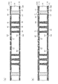
・図10(a)に示すように、貫通孔36の幅を、貫通孔37の幅よりも広くしてもよい。なお、図示の例では、2列目の貫通孔36の幅のみを広くしているが、1列目の貫通孔36の幅も同様に広くできる。
As shown in FIG. 10A, the width of the through
・上記実施形態に対し、貫通孔35の平面配置を適宜変更してもよい。例えば図7(c)に示したように、貫通孔35の短手方向に隣接する2つの貫通孔35を、長辺の位置が一致するように並列に配置してもよい。
-You may change suitably the planar arrangement | positioning of the through-
・図10(b)及び図10(c)に示すように、貫通孔37を省略し、貫通孔36のみを形成してもよい。このとき、図10(b)に示すように、各貫通孔36を、開口部34の角部周辺のみに形成してもよい。また、図10(c)に示すように、4つの貫通孔36によって開口部34の外周縁をなす各辺の大部分を囲むように各貫通孔36を形成してもよい。この場合のコア基板31には、隣接する2つの貫通孔36の間に橋部31Dが設けられている。なお、図10(b)及び図10(c)に示した例では、貫通孔36の列数を1列としているが、貫通孔36の列数は2列以上であってもよい。
-As shown in FIG.10 (b) and FIG.10 (c), the through-
・上記実施形態に対し、貫通孔35を充填する絶縁材(第1絶縁材)と、開口部34を充填する絶縁材(第2絶縁材)とを異なる絶縁材で構成してもよい。この場合には、貫通孔35を充填する絶縁材は、例えばコア基板31よりも熱膨張率の高い材料であることが好ましく、コア基板31よりも弾性率の低い材料であることが好ましい。また、開口部34を充填する絶縁材は、例えばコア基板31よりも熱膨張率の低い材料であることが好ましく、コア基板31よりも弾性率の低い材料であることが好ましい。
In contrast to the above embodiment, the insulating material (first insulating material) filling the through
この場合には、例えば図5(b)に示した工程において、まず、ディスペンサ等を用いて、コア基板31よりも熱膨張率の高い材料からなる液状の絶縁樹脂を貫通孔35に充填する。続いて、貫通孔35に充填された絶縁樹脂を熱硬化した後に、コア基板31よりも熱膨張率の低い材料からなる絶縁樹脂をラミネートして開口部34を充填する。
In this case, for example, in the process shown in FIG. 5B, first, the through-
・上記実施形態に対し、開口部34及び貫通孔35をストレート形状(断面視略矩形状)に形成してもよい。すなわち、開口部34及び貫通孔35の内壁面を、断面視において、コア基板31の第1面31Aに対して略垂直に延びるように形成してもよい。
-The
・上記実施形態に対し、配線部23の最上層の配線層85に半導体チップ91を実装してもよい。
・上記実施形態に対し、配線基板20に実装される半導体チップ91の数、その半導体チップ91の実装の形態(例えば、フリップチップ実装、ワイヤボンディングによる実装、又はこれらの組み合わせ)を適宜変更してもよい。
In contrast to the above embodiment, the
-The number of
・上記実施形態に対し、配線基板20に内蔵される電子部品50の数を適宜変更してもよい。
・上記実施形態の電子部品50としては、半導体チップに限らず、チップコンデンサ、チップ抵抗、インダクタ、薄膜コンデンサ等を採用してもよい。
-The number of the
The
・上記実施形態に対し、配線部22,23に含まれる絶縁層と配線層の層数を適宜変更してもよい。
・上記各実施形態並びに各変形例は適宜組み合わせてもよい。
-With respect to the said embodiment, you may change suitably the number of layers of the insulating layer and wiring layer which are contained in the
-Each above-mentioned embodiment and each modification may be combined suitably.
20 配線基板
21 コア部
22,23 配線部
31 コア基板
31A 第1面
31B 第2面
31D 橋部
34 開口部
35 貫通孔
36 貫通孔(第1貫通孔)
37 貫通孔(第2貫通孔)
50 電子部品
60 絶縁材
90 半導体装置
91 半導体チップ
100 フィルム
101,102 絶縁樹脂
DESCRIPTION OF
37 Through hole (second through hole)
50
Claims (10)
前記コア基板の第1面と該第1面と反対側の第2面との間を貫通し、平面形状が矩形状に形成された開口部と、
前記コア基板の第1面と第2面との間を貫通し、前記開口部と離間して形成された複数の第1貫通孔と、
前記開口部内に配置された電子部品と、
前記第1貫通孔に充填された第1絶縁材と、
前記開口部の内面と前記電子部品との間に充填された第2絶縁材と、を有し、
前記第1貫通孔は、平面視において、前記開口部の角部の周囲に、前記角部を構成する前記開口部の2つの辺に沿ってL字形に連続して形成されていること、
を特徴とする配線基板。 A core substrate;
An opening formed between the first surface of the core substrate and the second surface opposite to the first surface and having a planar shape formed in a rectangular shape;
A plurality of first through holes formed between the first surface and the second surface of the core substrate and spaced apart from the opening;
An electronic component disposed in the opening;
A first insulating material filled in the first through hole;
A second insulating material filled between the inner surface of the opening and the electronic component;
The first through hole is continuously formed in an L shape around two corners of the opening that forms the corner, around the corner of the opening in plan view,
A wiring board characterized by.
前記複数の第2貫通孔は、平面視において、隣接する前記第1貫通孔の間に、前記開口部の各辺に沿って並設され、
前記各第2貫通孔は、対向する前記辺に沿って長手が延びる長孔状に形成され、
前記第1絶縁材は、前記第2貫通孔に充填されていること、
を特徴とする請求項1に記載の配線基板。 A plurality of second through holes penetrating between the first surface and the second surface of the core substrate and spaced from the opening and the first through hole;
The plurality of second through holes are juxtaposed along each side of the opening between the adjacent first through holes in plan view,
Each of the second through holes is formed in a long hole shape extending in length along the opposing sides,
The first insulating material is filled in the second through hole;
The wiring board according to claim 1.
前記コア基板は、各列に配置された前記第2貫通孔同士の間に設けられた橋部を有し、
前記第2貫通孔の短手方向に隣接する2列の前記第2貫通孔は、前記2列のうち一方の列に設けられた前記橋部と、前記2列のうち他方の列に設けられた前記第2貫通孔とが対向するように配列されていることを特徴とする請求項2に記載の配線基板。 A plurality of rows of the second through holes are arranged around each side of the opening,
The core substrate has a bridge portion provided between the second through holes arranged in each row,
Two rows of the second through holes adjacent to each other in the short direction of the second through holes are provided in the bridge portion provided in one row of the two rows and in the other row of the two rows. The wiring board according to claim 2, wherein the second through holes are arranged so as to face each other.
前記第2貫通孔の短手方向に隣接する2つの前記第2貫通孔の間の長さは、前記第2貫通孔の短手方向の長さと同じ、又は前記第2貫通孔の短手方向の長さよりも長いこと、
を特徴とする請求項2又は3に記載の配線基板。 A plurality of rows of the second through holes are arranged around each side of the opening,
The length between two second through holes adjacent to each other in the short direction of the second through hole is the same as the length in the short direction of the second through hole, or the short direction of the second through hole. Longer than the length of
The wiring board according to claim 2, wherein:
を特徴とする請求項2〜4のいずれか一項に記載の配線基板。 M rows of second through holes are arranged around each side of the opening, and N rows of first through holes are arranged around each corner of the opening. about,
The wiring board according to any one of claims 2 to 4, wherein
を特徴とする請求項2〜5のいずれか一項に記載の配線基板。 The width of the first through hole is set wider than the length in the short direction of the second through hole;
The wiring board according to any one of claims 2 to 5, wherein:
を特徴とする請求項1〜6のいずれか一項に記載の配線基板。 A coefficient of thermal expansion of the first insulating material is higher than a coefficient of thermal expansion of the core substrate;
The wiring board according to claim 1, wherein:
を特徴とする請求項1〜7のいずれか一項に記載の配線基板。 The elastic modulus of the first insulating material is lower than the elastic modulus of the core substrate;
The wiring board according to claim 1, wherein:
前記コア基板の第1面側に形成された配線部に実装された半導体チップと、を有し、
前記第1貫通孔は、前記コア基板の第2面側から前記コア基板の第1面側に向かうに連れて幅が小さくなるように形成されていること、
を特徴とする半導体装置。 The wiring board according to any one of claims 1 to 8,
A semiconductor chip mounted on a wiring portion formed on the first surface side of the core substrate,
The first through hole is formed so that the width decreases from the second surface side of the core substrate toward the first surface side of the core substrate;
A semiconductor device characterized by the above.
前記コア基板の第1面と該第1面と反対側の第2面との間を貫通する開口部と、前記コア基板の第1面と第2面との間を貫通する第1貫通孔とを互いに離間して形成する工程と、
前記開口部を覆うフィルムを、前記コア基板の第1面側に貼着する工程と、
前記開口部内に電子部品を配置し、前記電子部品を前記フィルム上に固定する工程と、
前記第1貫通孔を充填する第1絶縁材を形成する工程と、
前記開口部を充填し、前記電子部品を固定する第2絶縁材を形成する工程と、
前記コア基板から前記フィルムを剥離する工程と、を有し、
前記開口部の平面形状は矩形状に形成され、
前記第1貫通孔は、平面視において、前記開口部の角部の周囲に、前記角部を構成する前記開口部の2つの辺に沿ってL字形に連続して形成されること、
を特徴とする配線基板の製造方法。 Preparing a core substrate; and
An opening that penetrates between the first surface of the core substrate and a second surface opposite to the first surface, and a first through hole that penetrates between the first surface and the second surface of the core substrate. And forming them separately from each other;
Bonding the film covering the opening to the first surface side of the core substrate;
Disposing an electronic component in the opening, and fixing the electronic component on the film;
Forming a first insulating material filling the first through hole;
Filling the opening and forming a second insulating material for fixing the electronic component;
Peeling the film from the core substrate,
The planar shape of the opening is formed in a rectangular shape,
The first through hole is continuously formed in an L shape around two corners of the opening constituting the corner, around the corner of the opening in plan view;
A method of manufacturing a wiring board, characterized in that
Priority Applications (2)
| Application Number | Priority Date | Filing Date | Title |
|---|---|---|---|
| JP2016021698A JP6639934B2 (en) | 2016-02-08 | 2016-02-08 | Wiring board, semiconductor device, and method of manufacturing wiring board |
| US15/425,390 US9799596B2 (en) | 2016-02-08 | 2017-02-06 | Wiring substrate and semiconductor device |
Applications Claiming Priority (1)
| Application Number | Priority Date | Filing Date | Title |
|---|---|---|---|
| JP2016021698A JP6639934B2 (en) | 2016-02-08 | 2016-02-08 | Wiring board, semiconductor device, and method of manufacturing wiring board |
Publications (2)
| Publication Number | Publication Date |
|---|---|
| JP2017143096A true JP2017143096A (en) | 2017-08-17 |
| JP6639934B2 JP6639934B2 (en) | 2020-02-05 |
Family
ID=59498073
Family Applications (1)
| Application Number | Title | Priority Date | Filing Date |
|---|---|---|---|
| JP2016021698A Active JP6639934B2 (en) | 2016-02-08 | 2016-02-08 | Wiring board, semiconductor device, and method of manufacturing wiring board |
Country Status (2)
| Country | Link |
|---|---|
| US (1) | US9799596B2 (en) |
| JP (1) | JP6639934B2 (en) |
Families Citing this family (3)
| Publication number | Priority date | Publication date | Assignee | Title |
|---|---|---|---|---|
| US11270920B2 (en) | 2018-08-14 | 2022-03-08 | Medtronic, Inc. | Integrated circuit package and method of forming same |
| KR102545168B1 (en) * | 2019-03-26 | 2023-06-19 | 삼성전자주식회사 | Interposer and semiconductor package including the same |
| KR20210007217A (en) * | 2019-07-10 | 2021-01-20 | 삼성전자주식회사 | An electronic device including an interposer |
Family Cites Families (4)
| Publication number | Priority date | Publication date | Assignee | Title |
|---|---|---|---|---|
| JP6009228B2 (en) * | 2012-05-30 | 2016-10-19 | 新光電気工業株式会社 | Manufacturing method of electronic component built-in substrate |
| JP6166878B2 (en) | 2012-08-30 | 2017-07-19 | 新光電気工業株式会社 | WIRING BOARD AND WIRING BOARD MANUFACTURING METHOD |
| JP5968753B2 (en) * | 2012-10-15 | 2016-08-10 | 新光電気工業株式会社 | Wiring board |
| JP6373605B2 (en) * | 2014-03-05 | 2018-08-15 | 新光電気工業株式会社 | WIRING BOARD AND WIRING BOARD MANUFACTURING METHOD |
-
2016
- 2016-02-08 JP JP2016021698A patent/JP6639934B2/en active Active
-
2017
- 2017-02-06 US US15/425,390 patent/US9799596B2/en active Active
Also Published As
| Publication number | Publication date |
|---|---|
| JP6639934B2 (en) | 2020-02-05 |
| US20170229388A1 (en) | 2017-08-10 |
| US9799596B2 (en) | 2017-10-24 |
Similar Documents
| Publication | Publication Date | Title |
|---|---|---|
| JP6173781B2 (en) | Wiring board and method of manufacturing wiring board | |
| JP5410660B2 (en) | WIRING BOARD AND ITS MANUFACTURING METHOD, ELECTRONIC COMPONENT DEVICE AND ITS MANUFACTURING METHOD | |
| JP5389770B2 (en) | Printed circuit board with built-in electronic element and manufacturing method thereof | |
| US20100208442A1 (en) | Wiring board assembly and manufacturing method thereof | |
| US9951434B2 (en) | Printed wiring board, semiconductor package and method for manufacturing printed wiring board | |
| US10098243B2 (en) | Printed wiring board and semiconductor package | |
| JP2015106615A (en) | Printed wiring board and method for manufacturing printed wiring board | |
| WO2007126090A1 (en) | Circuit board, electronic device and method for manufacturing circuit board | |
| JP6158601B2 (en) | Wiring board and method of manufacturing wiring board | |
| JP7202785B2 (en) | Wiring board and method for manufacturing wiring board | |
| JP2013532901A (en) | Heat dissipation circuit board and manufacturing method thereof | |
| JP2017034059A (en) | Printed wiring board, semiconductor package and manufacturing method for printed wiring board | |
| JP2015225895A (en) | Printed wiring board, semiconductor package and printed wiring board manufacturing method | |
| JP6228851B2 (en) | Wiring board, method for manufacturing wiring board | |
| KR101139084B1 (en) | Multilayer printed circuit board and method of making same | |
| JP2009252942A (en) | Component built-in wiring board, and method of manufacturing component built-in wiring board | |
| JP2010226075A (en) | Wiring board and method for manufacturing the same | |
| JP6639934B2 (en) | Wiring board, semiconductor device, and method of manufacturing wiring board | |
| JP2009135391A (en) | Electronic device and method of manufacturing the same | |
| US9420696B2 (en) | Method of manufacturing wiring substrate | |
| JP7247046B2 (en) | Wiring board and method for manufacturing wiring board | |
| JP2011151048A (en) | Method of manufacturing electronic component, and electronic component | |
| JP2009231431A (en) | Multilayer printed-wiring board and semiconductor device using the same | |
| JP2008311508A (en) | Electronic component package and manufacturing method thereof | |
| JP2002164475A (en) | Semiconductor device |
Legal Events
| Date | Code | Title | Description |
|---|---|---|---|
| A621 | Written request for application examination |
Free format text: JAPANESE INTERMEDIATE CODE: A621 Effective date: 20181121 |
|
| A977 | Report on retrieval |
Free format text: JAPANESE INTERMEDIATE CODE: A971007 Effective date: 20190807 |
|
| A131 | Notification of reasons for refusal |
Free format text: JAPANESE INTERMEDIATE CODE: A131 Effective date: 20190820 |
|
| A521 | Request for written amendment filed |
Free format text: JAPANESE INTERMEDIATE CODE: A523 Effective date: 20190917 |
|
| TRDD | Decision of grant or rejection written | ||
| A01 | Written decision to grant a patent or to grant a registration (utility model) |
Free format text: JAPANESE INTERMEDIATE CODE: A01 Effective date: 20191210 |
|
| A61 | First payment of annual fees (during grant procedure) |
Free format text: JAPANESE INTERMEDIATE CODE: A61 Effective date: 20191225 |
|
| R150 | Certificate of patent or registration of utility model |
Ref document number: 6639934 Country of ref document: JP Free format text: JAPANESE INTERMEDIATE CODE: R150 |