JP2017142080A - Contact terminal, inspection tool, and inspection device - Google Patents
Contact terminal, inspection tool, and inspection device Download PDFInfo
- Publication number
- JP2017142080A JP2017142080A JP2016021869A JP2016021869A JP2017142080A JP 2017142080 A JP2017142080 A JP 2017142080A JP 2016021869 A JP2016021869 A JP 2016021869A JP 2016021869 A JP2016021869 A JP 2016021869A JP 2017142080 A JP2017142080 A JP 2017142080A
- Authority
- JP
- Japan
- Prior art keywords
- cylindrical body
- spring
- inspection
- spring portion
- contact terminal
- Prior art date
- Legal status (The legal status is an assumption and is not a legal conclusion. Google has not performed a legal analysis and makes no representation as to the accuracy of the status listed.)
- Pending
Links
Images


Classifications
-
- G—PHYSICS
- G01—MEASURING; TESTING
- G01R—MEASURING ELECTRIC VARIABLES; MEASURING MAGNETIC VARIABLES
- G01R1/00—Details of instruments or arrangements of the types included in groups G01R5/00 - G01R13/00 and G01R31/00
- G01R1/02—General constructional details
- G01R1/06—Measuring leads; Measuring probes
- G01R1/067—Measuring probes
- G01R1/06711—Probe needles; Cantilever beams; "Bump" contacts; Replaceable probe pins
- G01R1/06716—Elastic
- G01R1/06722—Spring-loaded
-
- G—PHYSICS
- G01—MEASURING; TESTING
- G01R—MEASURING ELECTRIC VARIABLES; MEASURING MAGNETIC VARIABLES
- G01R1/00—Details of instruments or arrangements of the types included in groups G01R5/00 - G01R13/00 and G01R31/00
- G01R1/20—Modifications of basic electric elements for use in electric measuring instruments; Structural combinations of such elements with such instruments
-
- G—PHYSICS
- G01—MEASURING; TESTING
- G01R—MEASURING ELECTRIC VARIABLES; MEASURING MAGNETIC VARIABLES
- G01R31/00—Arrangements for testing electric properties; Arrangements for locating electric faults; Arrangements for electrical testing characterised by what is being tested not provided for elsewhere
- G01R31/28—Testing of electronic circuits, e.g. by signal tracer
- G01R31/2801—Testing of printed circuits, backplanes, motherboards, hybrid circuits or carriers for multichip packages [MCP]
- G01R31/2806—Apparatus therefor, e.g. test stations, drivers, analysers, conveyors
- G01R31/2808—Holding, conveying or contacting devices, e.g. test adapters, edge connectors, extender boards
-
- G—PHYSICS
- G01—MEASURING; TESTING
- G01R—MEASURING ELECTRIC VARIABLES; MEASURING MAGNETIC VARIABLES
- G01R31/00—Arrangements for testing electric properties; Arrangements for locating electric faults; Arrangements for electrical testing characterised by what is being tested not provided for elsewhere
- G01R31/28—Testing of electronic circuits, e.g. by signal tracer
- G01R31/2851—Testing of integrated circuits [IC]
- G01R31/2886—Features relating to contacting the IC under test, e.g. probe heads; chucks
-
- G—PHYSICS
- G01—MEASURING; TESTING
- G01R—MEASURING ELECTRIC VARIABLES; MEASURING MAGNETIC VARIABLES
- G01R1/00—Details of instruments or arrangements of the types included in groups G01R5/00 - G01R13/00 and G01R31/00
- G01R1/02—General constructional details
- G01R1/06—Measuring leads; Measuring probes
- G01R1/067—Measuring probes
- G01R1/06772—High frequency probes
Abstract
Description
本発明は、対象物に接触させるための接触端子、その接触端子を支持する検査治具、及びその検査治具を備えた検査装置に関する。 The present invention relates to a contact terminal for contacting an object, an inspection jig for supporting the contact terminal, and an inspection apparatus including the inspection jig.
従来より、所定の対象点に棒状の接触端子を接触させることで、対象点と所定箇所とを電気的に接続するための接触端子が知られている(例えば、特許文献1参照。)。特許文献1に記載の接触端子は、小径の導電部とそれを囲むように配置された大径の円筒形状部とを備え、小径の導電部の先端部が、大径の円筒形状部の先端部から突出し、小径の導電部の一部が、大径の円筒形状部の一部に接合されている。この接触端子の円筒形状部には、螺旋形状のばねが形成されている。 Conventionally, a contact terminal for electrically connecting a target point and a predetermined location by bringing a rod-shaped contact terminal into contact with the predetermined target point is known (see, for example, Patent Document 1). The contact terminal described in Patent Document 1 includes a small-diameter conductive portion and a large-diameter cylindrical portion disposed so as to surround the conductive portion, and the tip of the small-diameter conductive portion is the tip of the large-diameter cylindrical portion. A part of the small-diameter conductive part protrudes from the part and is joined to a part of the large-diameter cylindrical part. A spiral spring is formed on the cylindrical portion of the contact terminal.
しかしながら、上述の接触端子によれば、接触端子に接触された対象点を検査するためにこの接触端子に検査用の電流を流すと、その電流が螺旋形状のばねを流れる。螺旋形状のばねはコイルと同様に機能するから、いわゆる右ねじの法則(右手の法則)に従い磁界が発生する。そのため、このようにして発生した磁界が、検査結果に影響を与えるおそれがあった。 However, according to the contact terminal described above, when an inspection current is passed through the contact terminal in order to inspect the target point that is in contact with the contact terminal, the current flows through the spiral spring. Since the spiral spring functions in the same way as a coil, a magnetic field is generated in accordance with the so-called right-hand rule (right-hand rule). For this reason, the magnetic field generated in this way may affect the inspection result.
本発明の目的は、検査に伴う磁界の発生を低減することができる接触端子、検査治具、及び検査装置を提供することである。 The objective of this invention is providing the contact terminal which can reduce generation | occurrence | production of the magnetic field accompanying a test | inspection, a test | inspection jig, and a test | inspection apparatus.
本発明に係る接触端子は、導電性を有する筒状の外側筒状体と、前記外側筒状体の筒内に挿通された導電性を有する筒状の内側筒状体とを備え、前記外側筒状体に、当該外側筒状体の軸方向に伸縮すると共に巻き方向が第一方向の螺旋状の外側第一ばね部が形成され、前記内側筒状体に、当該内側筒状体の軸方向に伸縮すると共に巻き方向が前記第一方向とは逆方向である第二方向の螺旋状の内側第一ばね部が形成されている。 A contact terminal according to the present invention includes a cylindrical outer cylindrical body having conductivity, and a cylindrical inner cylindrical body having conductivity inserted into a cylinder of the outer cylindrical body, A spiral outer first spring portion having a first winding direction and extending and contracting in the axial direction of the outer cylindrical body is formed on the cylindrical body, and the inner cylindrical body has an axis of the inner cylindrical body. A spiral inner first spring portion is formed in a second direction that expands and contracts in the direction and has a winding direction opposite to the first direction.
この構成によれば、外側第一ばね部と内側第一ばね部とは、巻き方向が互いに逆方向にされているので、外側筒状体と内側筒状体とに電流が流れた場合、外側第一ばね部で生じる磁界と内側第一ばね部で生じる磁界とは、方向が逆の磁界になる結果、互いに相殺し合うことになる。その結果、検査に伴う磁界の発生を低減することができる。 According to this configuration, the winding direction of the outer first spring portion and the inner first spring portion is opposite to each other. Therefore, when a current flows through the outer cylindrical body and the inner cylindrical body, The magnetic field generated in the first spring portion and the magnetic field generated in the inner first spring portion cancel each other as a result of the magnetic fields having opposite directions. As a result, it is possible to reduce the generation of a magnetic field accompanying the inspection.
また、前記内側第一ばね部は、前記外側第一ばね部と対向する位置に位置していることが好ましい。 Moreover, it is preferable that the said inner side 1st spring part is located in the position facing the said outer side 1st spring part.
この構成によれば、外側第一ばね部の内側に内側第一ばね部が配置されることになるので、外側第一ばね部で生じた磁界と内側第一ばね部で生じた磁界とを、効率よく相殺することが可能となる。 According to this configuration, since the inner first spring part is disposed inside the outer first spring part, the magnetic field generated in the outer first spring part and the magnetic field generated in the inner first spring part are It becomes possible to cancel out efficiently.
また、前記外側筒状体には、さらに、巻き方向が前記第二方向の外側第二ばね部が形成され、前記内側筒状体には、さらに、巻き方向が前記第一方向の内側第二ばね部が形成されていることが好ましい。 The outer cylindrical body further includes an outer second spring portion whose winding direction is the second direction, and the inner cylindrical body further has an inner second spring whose winding direction is the first direction. A spring portion is preferably formed.
この構成によれば、外側筒状体には、巻き方向が互いに逆方向にされた外側第一ばね部と外側第二ばね部とが形成される。従って、外側第一ばね部と外側第二ばね部とが伸縮する際に、外側第一ばね部で生じる回転力と外側第二ばね部で生じる回転力とが逆方向となり、互いの回転力が相殺されるので、対象物に接触端子を接触させる際に生じる外側筒状体の動きを低減することができる。また、内側筒状体には、巻き方向が互いに逆方向にされた内側第一ばね部と内側第二ばね部とが形成される。従って、内側第一ばね部と内側第二ばね部とが伸縮する際に、内側第一ばね部で生じる回転力と内側第二ばね部で生じる回転力とが逆方向となり、互いの回転力が相殺されるので、対象物に接触端子を接触させる際に生じる内側筒状体の動きを低減することができる。 According to this configuration, the outer cylindrical body is formed with the outer first spring portion and the outer second spring portion whose winding directions are opposite to each other. Therefore, when the outer first spring portion and the outer second spring portion expand and contract, the rotational force generated in the outer first spring portion and the rotational force generated in the outer second spring portion are in opposite directions, and the mutual rotational force is Since it cancels, the movement of the outer cylindrical body that occurs when the contact terminal is brought into contact with the object can be reduced. Further, the inner cylindrical body is formed with an inner first spring portion and an inner second spring portion whose winding directions are opposite to each other. Therefore, when the inner first spring portion and the inner second spring portion expand and contract, the rotational force generated in the inner first spring portion and the rotational force generated in the inner second spring portion are in opposite directions, and the mutual rotational force is Since they are offset, the movement of the inner cylindrical body that occurs when the contact terminal is brought into contact with the object can be reduced.
また、前記内側第二ばね部は、前記外側第二ばね部と対向する位置に位置していることが好ましい。 Moreover, it is preferable that the said inside 2nd spring part is located in the position facing the said outside 2nd spring part.
この構成によれば、外側第二ばね部の内側に内側第二ばね部が配置されることになるので、外側第二ばね部で生じた磁界と内側第二ばね部で生じた磁界とを、効率よく相殺することが可能となる。 According to this configuration, since the inner second spring portion is disposed inside the outer second spring portion, the magnetic field generated in the outer second spring portion and the magnetic field generated in the inner second spring portion are It becomes possible to cancel out efficiently.
また、前記外側第一ばね部の巻き数と、前記内側第一ばね部の巻き数とが略同数であることが好ましい。 Moreover, it is preferable that the number of turns of the outer first spring part and the number of turns of the inner first spring part are substantially the same.
外側第一ばね部の巻き数と、内側第一ばね部の巻き数とが略同数であると、外側第一ばね部で生じる磁界強度と内側第一ばね部で生じる磁界強度とが略等しくなる。その結果、外側第一ばね部で生じる磁界と内側第一ばね部で生じる磁界とが相殺される精度が向上する。 When the number of turns of the outer first spring part and the number of turns of the inner first spring part are substantially the same, the magnetic field strength generated in the outer first spring part and the magnetic field intensity generated in the inner first spring part become substantially equal. . As a result, the accuracy with which the magnetic field generated in the outer first spring portion and the magnetic field generated in the inner first spring portion are offset is improved.
また、前記外側第一ばね部は、前記外側筒状体の複数箇所に形成され、前記内側第一ばね部は、前記内側筒状体の、前記外側第一ばね部と同数の箇所に形成され、前記複数箇所の外側第一ばね部の螺旋の巻き数の合計と、前記複数箇所の内側第一ばね部の螺旋の巻き数の合計とが略等しい構成であってもよい。 The outer first spring portion is formed at a plurality of locations on the outer cylindrical body, and the inner first spring portion is formed at the same number of locations on the inner cylindrical body as the outer first spring portion. The total number of spiral turns of the plurality of outer first spring portions may be substantially equal to the total number of spiral turns of the plurality of inner first spring portions.
この構成によれば、外側第一ばね部と内側第一ばね部とをそれぞれ複数設けつつ、接続端子全体として、外側第一ばね部で生じた磁界と内側第一ばね部で生じた磁界とを相殺することができる。 According to this configuration, a plurality of outer first spring portions and inner first spring portions are provided, and a magnetic field generated in the outer first spring portion and a magnetic field generated in the inner first spring portion are formed as the entire connection terminal. Can be offset.
また、前記複数の外側第一ばね部と、前記複数の内側第一ばね部とは、それぞれ互いに対向する位置に位置し、前記複数の外側第一ばね部と、前記複数の内側第一ばね部とは、互いに対向して位置するもの同士で前記螺旋の巻き数が略等しいことが好ましい。 The plurality of outer first spring portions and the plurality of inner first spring portions are located at positions facing each other, the plurality of outer first spring portions, and the plurality of inner first spring portions. It is preferable that the number of turns of the spiral is substantially equal between those facing each other.
この構成によれば、複数の外側第一ばね部の内側に、それぞれ内側第一ばね部が配置されることになるので、外側第一ばね部で生じた磁界と内側第一ばね部で生じた磁界とを、効率よく相殺することが可能となる。 According to this configuration, since the inner first spring portion is disposed inside each of the plurality of outer first spring portions, the magnetic field generated in the outer first spring portion and the inner first spring portion are generated. It is possible to efficiently cancel the magnetic field.
また、前記外側第二ばね部の巻き数と、前記内側第二ばね部の巻き数とが略同数であることが好ましい。 Moreover, it is preferable that the number of turns of the outer second spring part and the number of turns of the inner second spring part are substantially the same.
外側第二ばね部の巻き数と、内側第二ばね部の巻き数とが略同数であると、外側第二ばね部で生じる磁界強度と内側第二ばね部で生じる磁界強度とが略等しくなる。その結果、外側第二ばね部で生じる磁界と内側第二ばね部で生じる磁界とが相殺される精度が向上する。 When the number of turns of the outer second spring part and the number of turns of the inner second spring part are substantially the same, the magnetic field strength generated at the outer second spring part and the magnetic field intensity generated at the inner second spring part become substantially equal. . As a result, the accuracy with which the magnetic field generated in the outer second spring portion and the magnetic field generated in the inner second spring portion are offset is improved.
また、前記外側第二ばね部は、前記外側筒状体の複数箇所に形成され、前記内側第二ばね部は、前記内側筒状体の、前記外側第二ばね部と同数の箇所に形成され、前記複数箇所の外側第二ばね部の螺旋の巻き数の合計と、前記複数箇所の内側第二ばね部の螺旋の巻き数の合計とが略等しいことが好ましい。 The outer second spring portion is formed at a plurality of locations on the outer cylindrical body, and the inner second spring portion is formed at the same number of locations as the outer second spring portion of the inner cylindrical body. Preferably, the total number of spiral turns of the plurality of outer second spring portions and the total number of spiral turns of the plurality of inner second spring portions are substantially equal.
この構成によれば、外側第二ばね部と内側第二ばね部とをそれぞれ複数設けつつ、接続端子全体として、外側第二ばね部で生じた磁界と内側第二ばね部で生じた磁界とを相殺することができる。 According to this configuration, while providing a plurality of outer second spring portions and inner second spring portions, respectively, the magnetic field generated in the outer second spring portion and the magnetic field generated in the inner second spring portion as a whole connection terminal. Can be offset.
また、前記複数の外側第二ばね部と、前記内側第二ばね部とは、それぞれ互いに対向する位置に位置し、前記複数の外側第二ばね部と、前記複数の内側第二ばね部とは、互いに対向して位置するもの同士で前記螺旋の巻き数が略等しい。 Further, the plurality of outer second spring portions and the inner second spring portion are located at positions facing each other, and the plurality of outer second spring portions and the plurality of inner second spring portions are The number of turns of the spiral is substantially the same between those facing each other.
この構成によれば、複数の外側第二ばね部の内側に、それぞれ内側第二ばね部が配置されることになるので、外側第二ばね部で生じた磁界と内側第二ばね部で生じた磁界とを、効率よく相殺することが可能となる。 According to this configuration, since the inner second spring portions are respectively arranged inside the plurality of outer second spring portions, the magnetic field generated in the outer second spring portion and the inner second spring portion are generated. It is possible to efficiently cancel the magnetic field.
また、前記内側筒状体の筒内に挿通された導電性を有する棒状の中心導体をさらに備えることが好ましい。 Moreover, it is preferable to further provide a conductive rod-shaped center conductor inserted into the cylinder of the inner cylindrical body.
この構成によれば、接触させようとする対象物に棒状の中心導体を接触させることができるので、接触状態を安定化することができる。 According to this configuration, since the rod-shaped center conductor can be brought into contact with the object to be brought into contact, the contact state can be stabilized.
また、前記外側筒状体及び前記内側筒状体のうち少なくとも一方の、一端側の端面に対する垂線は、当該少なくとも一方の軸線に対して傾斜していることが好ましい。 Moreover, it is preferable that the perpendicular to the end surface on one end side of at least one of the outer cylindrical body and the inner cylindrical body is inclined with respect to the at least one axis.
この構成によれば、外側筒状体及び内側筒状体のうち少なくとも一方の一端側の端面の傾斜に応じて、当該少なくとも一方の筒状体を撓みやすくすることができる。筒状体が撓むと、筒状体と中心導体とが接触し易くなる結果、筒状体と中心導体とを導通させる確実性が向上する。 According to this configuration, the at least one cylindrical body can be easily bent according to the inclination of the end face on at least one end side of the outer cylindrical body and the inner cylindrical body. When the tubular body is bent, the tubular body and the central conductor are easily brought into contact with each other. As a result, the certainty of conducting the tubular body and the central conductor is improved.
また、本発明に係る検査治具は、上述の接触端子を複数備え、前記複数の接触端子を支持する支持部材を備える。 In addition, an inspection jig according to the present invention includes a plurality of the above-described contact terminals, and includes a support member that supports the plurality of contact terminals.
この構成によれば、複数の接触端子を支持する検査治具を用いた検査の際に、検査に伴う磁界の発生を低減することができる。 According to this configuration, it is possible to reduce the generation of a magnetic field associated with the inspection during the inspection using the inspection jig that supports the plurality of contact terminals.
また、本発明に係る検査装置は、上述の検査治具と、前記接触端子を検査対象物に設けられた検査点に接触させ、当該接触端子から得られる電気信号に基づき前記検査対象物の検査を行う検査処理部とを備える。 The inspection apparatus according to the present invention is configured to bring the inspection jig and the contact terminal into contact with an inspection point provided on the inspection object, and to inspect the inspection object based on an electrical signal obtained from the contact terminal. An inspection processing unit.
この検査装置によれば、検査に伴う磁界の発生を低減することができる。 According to this inspection apparatus, generation of a magnetic field accompanying inspection can be reduced.
このような構成の接触端子、検査治具、及び検査装置は、検査に伴う磁界の発生を低減することができる。 The contact terminal, the inspection jig, and the inspection apparatus having such a configuration can reduce the generation of a magnetic field due to the inspection.
以下、本発明に係る実施形態を図面に基づいて説明する。なお、各図において同一の符号を付した構成は、同一の構成であることを示し、その説明を省略する。図1は、本発明の一実施形態に係る接触端子及び検査治具を備えた基板検査装置1の構成を概略的に示す概念図である。基板検査装置1は、検査装置の一例に相当している。図1に示す基板検査装置1は、検査対象物の一例である基板100に形成された回路パターンを検査するための装置である。
Embodiments according to the present invention will be described below with reference to the drawings. In addition, the structure which attached | subjected the same code | symbol in each figure shows that it is the same structure, The description is abbreviate | omitted. FIG. 1 is a conceptual diagram schematically showing a configuration of a substrate inspection apparatus 1 including a contact terminal and an inspection jig according to an embodiment of the present invention. The substrate inspection apparatus 1 corresponds to an example of an inspection apparatus. A substrate inspection apparatus 1 shown in FIG. 1 is an apparatus for inspecting a circuit pattern formed on a
基板100は、例えばプリント配線基板、フレキシブル基板、セラミック多層配線基板、液晶ディスプレイやプラズマディスプレイ用の電極板、半導体基板、及び半導体パッケージ用のパッケージ基板やフィルムキャリアなど種々の基板であってもよい。なお、検査対象物は、基板に限らず、例えば半導体素子(IC:Integrated Circuit)等の電子部品であってもよく、その他電気的な検査を行う対象となるものであればよい。
The
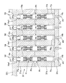
図1に示す基板検査装置1は、検査部4U,4Dと、基板固定装置6と、検査処理部8とを備えている。基板固定装置6は、検査対象の基板100を所定の位置に固定するように構成されている。検査部4U,4Dは、検査治具3U,3Dと、検査治具3U,3Dが取り付けられるプレート321とを備えている。検査部4U,4Dは、図略の駆動機構によって、検査治具3U,3Dを、互いに直交するX,Y,Zの三軸方向に移動可能にされ、さらに検査治具3U,3Dを、Z軸を中心に回動可能にされている。
A substrate inspection apparatus 1 shown in FIG. 1 includes
検査部4Uは、基板固定装置6に固定された基板100の上方に位置する。検査部4Dは、基板固定装置6に固定された基板100の下方に位置する。検査部4U,4Dは、基板100に形成された回路パターンを検査するための検査治具3U,3Dを着脱可能に構成されている。以下、検査部4U,4Dを総称して検査部4と称する。
The
検査治具3U,3Dは、それぞれ、複数のプローブPr(接触端子)と、複数のプローブPrを、先端を基板100へ向けて保持する支持ブロック31とを備えている。プローブPrは接触端子の一例に相当している。プレート321には、各プローブPrの後端と接触して導通する電極が設けられている。検査部4U,4Dは、プレート321の各電極を介して各プローブPrの後端を、検査処理部8と電気的に接続したり、その接続を切り替えたりする図略の接続回路を備えている。
Each of the inspection jigs 3U and 3D includes a plurality of probes Pr (contact terminals) and a
プローブPrは、棒状の形状を有している。プローブPrの構成の詳細については後述する。支持ブロック31には、プローブPrを支持する複数の貫通孔が形成されている。各貫通孔は、検査対象となる基板100の配線パターン上に設定された検査点の位置と対応するように配置されている。これにより、プローブPrの先端部が基板100の検査点に接触するようにされている。例えば、複数のプローブPrは、格子の交点位置に対応するように配設されている。当該格子の桟に相当する方向が、互いに直交するX軸方向及びY軸方向と一致するようにされている。検査点は、例えば配線パターン、半田バンプ、接続端子等とされている。
The probe Pr has a rod shape. Details of the configuration of the probe Pr will be described later. A plurality of through holes that support the probe Pr are formed in the
検査治具3U,3Dは、プローブPrの配置が異なる点と、検査部4U,4Dへの取り付け方向が上下逆になる点を除き、互いに同様に構成されている。以下、検査治具3U,3Dを総称して検査治具3と称する。検査治具3は、検査対象の基板100に応じて取り替え可能にされている。
The inspection jigs 3U and 3D are configured in the same manner except that the arrangement of the probes Pr is different and that the mounting directions to the
検査処理部8は、例えば電源回路、電圧計、電流計、及びマイクロコンピュータ等を備えている。検査処理部8は、図略の駆動機構を制御して検査部4U,4Dを移動、位置決めさせ、基板100の各検査点に、各プローブPrの先端を接触させる。これにより、各検査点と、検査処理部8とが電気的に接続される。この状態で、検査処理部8は、検査治具3の各プローブPrを介して基板100の各検査点に検査用の電流又は電圧を供給し、各プローブPrから得られた電圧信号又は電流信号に基づき、例えば回路パターンの断線や短絡等の基板100の検査を実行する。あるいは、検査処理部8は、交流の電流又は電圧を各検査点に供給することによって各プローブPrから得られた電圧信号又は電流信号に基づき、検査対象のインピーダンスを測定してもよい。
The
図2は、図1に示す支持ブロック31及びプレート321の構成の一例を示す模式図である。図2に示す支持ブロック31は、例えば板状の支持プレート31a,31b,31cが積層されて構成されている。支持プレート31cが支持ブロック31の先端側、支持プレート31aが支持ブロック31の後端側となるようにされている。そして、支持プレート31a,31b,31cを貫通するように、複数の貫通孔Hが形成されている。
FIG. 2 is a schematic diagram showing an example of the configuration of the
支持プレート31a,31bの貫通孔が孔部Haとされている。支持プレート31cの貫通孔が狭隘部Hbとされている。支持プレート31aの、プレート321と対向する面に孔部Haが開口する側すなわち孔部Haの後端側は、孔径が小さくされた小径部Ha1とされている。そして、孔部Haと狭隘部Hbとが連通されて、貫通孔Hが形成されている。
The through holes of the
なお、支持部材の一例である支持ブロック31は、板状の支持プレート31a,31b,31cが積層されて構成される例に限らない。支持部材は、例えば一体の部材に孔部Haと狭隘部Hbとが形成されて貫通孔Hとされていてもよい。また、必ずしも狭隘部Hbが形成されている例に限られず、貫通孔H全体が孔部Haとされていてもよい。また、孔部Haに小径部Ha1が形成されていなくてもよい。また、支持部材の支持プレート31a,31bが積層された構成を示したが、支持プレート31aと支持プレート31bとが離間した状態で例えば支柱等により支えられた構成であってもよい。
In addition, the
支持プレート31aの後端側には、例えば絶縁性の樹脂材料により構成されたプレート321が取り付けられている。プレート321によって、貫通孔Hの後端側開口部Hcが閉塞されている。プレート321の、各後端側開口部Hcと対向する箇所には、配線34が、プレート321を貫通するように取り付けられている。プレート321の、支持プレート31aに面する側の表面と、その面に露出する配線34の端面とが面一になるようにされている。その配線34の端面は、電極34aとされている。
A
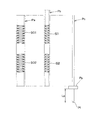
各貫通孔Hには、プローブPrが挿入されている。プローブPrは、導電性を有する筒状の外側筒状体Paと、外側筒状体Paの筒内に挿通された導電性を有する筒状の内側筒状体Pbと、内側筒状体Pbの筒内に挿通された導電性を有する棒状の中心導体Pcとを備えている。 A probe Pr is inserted into each through hole H. The probe Pr includes a cylindrical outer cylindrical body Pa having conductivity, a cylindrical inner cylindrical body Pb having conductivity inserted into a cylinder of the outer cylindrical body Pa, and an inner cylindrical body Pb. And a conductive rod-shaped central conductor Pc inserted into the cylinder.
図3は、プローブPrを、外側筒状体Pa、内側筒状体Pb、及び中心導体Pcに分解して示す平面図である。外側筒状体Paには、外側筒状体Paの軸方向に伸縮すると共に巻き方向が第一方向の螺旋状の外側第一ばね部SO1と、巻き方向が第一方向とは逆方向の螺旋状である第二方向の外側第二ばね部SO2とが形成されている。また、外側第一ばね部SO1と外側第二ばね部SO2とは、螺旋の巻き数及び線幅が略同一にされている。 FIG. 3 is a plan view showing the probe Pr disassembled into an outer cylindrical body Pa, an inner cylindrical body Pb, and a central conductor Pc. The outer cylindrical body Pa includes a spiral outer first spring portion SO1 that expands and contracts in the axial direction of the outer cylindrical body Pa and has a winding direction in the first direction, and a spiral in which the winding direction is opposite to the first direction. The outer second spring portion SO2 in the second direction is formed. The outer first spring portion SO1 and the outer second spring portion SO2 have substantially the same number of spiral turns and the same line width.
外側筒状体Paの外径は、小径部Ha1の内径より大きくされている。これにより、貫通孔Hに挿通されたプローブPrが小径部Ha1から抜け落ちないようにされている。なお、小径部Ha1を設けず、外側筒状体Paと内側筒状体Pbとを同じ長さにしてもよい。 The outer diameter of the outer cylindrical body Pa is larger than the inner diameter of the small diameter portion Ha1. Thereby, the probe Pr inserted through the through hole H is prevented from falling off from the small diameter portion Ha1. Note that the outer cylindrical body Pa and the inner cylindrical body Pb may have the same length without providing the small diameter portion Ha1.
内側筒状体Pbには、内側筒状体Pbの軸方向に伸縮すると共に巻き方向が第二方向の螺旋状である内側第一ばね部SI1と、巻き方向が第一方向の螺旋状である内側第二ばね部SI2とが形成されている。内側第一ばね部SI1と、内側第二ばね部SI2とは、螺旋の巻き数及び線幅が略同一にされている。 The inner cylindrical body Pb has an inner first spring portion SI1 that expands and contracts in the axial direction of the inner cylindrical body Pb and the spiral direction is the second direction, and the spiral direction is the spiral direction of the first direction. An inner second spring portion SI2 is formed. The inner first spring portion SI1 and the inner second spring portion SI2 have substantially the same number of spiral turns and the same line width.
内側筒状体Pbの外径は、外側筒状体Paの内径よりも細くされており、内側筒状体Pbが外側筒状体Paの筒内に挿通されるようになっている。また、内側筒状体Pbは、外側筒状体Paよりも長くされている。外側筒状体Pa及び内側筒状体Pbの材料としては、例えばニッケルあるいはニッケル合金を用いることができる。 The outer diameter of the inner cylindrical body Pb is smaller than the inner diameter of the outer cylindrical body Pa, and the inner cylindrical body Pb is inserted into the cylinder of the outer cylindrical body Pa. The inner cylindrical body Pb is longer than the outer cylindrical body Pa. As a material of the outer cylindrical body Pa and the inner cylindrical body Pb, for example, nickel or a nickel alloy can be used.
内側第一ばね部SI1、内側第二ばね部SI2、外側第一ばね部SO1、及び外側第二ばね部SO2等のばね部の形成方法は特に限定されないが、筒状の部材の周壁を例えばエッチングして螺旋状のスリットを形成することでばね部を形成してもよく、例えば電鋳により筒状の部材の周壁に螺旋状のスリットが設けられた形状を形成することでばね部を形成してもよく、種々の製造方法を用いることができる。 The method of forming the spring parts such as the inner first spring part SI1, the inner second spring part SI2, the outer first spring part SO1, and the outer second spring part SO2 is not particularly limited. For example, the peripheral wall of the cylindrical member is etched. The spring portion may be formed by forming a spiral slit, and for example, the spring portion may be formed by forming a shape in which the spiral slit is provided on the peripheral wall of the cylindrical member by electroforming. Various manufacturing methods may be used.
中心導体Pcは、略円柱形状を有し、内側筒状体Pbの筒内に挿通されている。中心導体Pcの先端部Pf付近には、周囲にフランジ状に突起する突起部Ppが設けられている。中心導体Pcの直径は、狭隘部Hbの内径よりも細くされている。突起部Ppの直径は、狭隘部Hbの内径よりも大きく、かつ外側筒状体Paの外径以上にされている。中心導体Pcとしては、例えばハンダが付きにくいパラジウム合金を好適に用いることができる。 The center conductor Pc has a substantially cylindrical shape, and is inserted into the cylinder of the inner cylindrical body Pb. In the vicinity of the front end portion Pf of the center conductor Pc, there is provided a protrusion Pp that protrudes in the form of a flange around the periphery. The diameter of the center conductor Pc is smaller than the inner diameter of the narrow portion Hb. The diameter of the projecting portion Pp is larger than the inner diameter of the narrow portion Hb and larger than the outer diameter of the outer cylindrical body Pa. As the center conductor Pc, for example, a palladium alloy that is difficult to be soldered can be suitably used.
外側筒状体Paの内径と内側筒状体Pbの外径との差、及び内側筒状体Pbの内径と中心導体Pcの外径との差は微小にされている。その結果、外側筒状体Pa、内側筒状体Pb、及び中心導体Pcが互いに摺動可能な状態で接触し、電気的に導通するようにされている。 The difference between the inner diameter of the outer cylindrical body Pa and the outer diameter of the inner cylindrical body Pb, and the difference between the inner diameter of the inner cylindrical body Pb and the outer diameter of the center conductor Pc are made minute. As a result, the outer cylindrical body Pa, the inner cylindrical body Pb, and the central conductor Pc are in contact with each other in a slidable state, and are electrically connected.
また、突起部Ppの先端向きの面から先端部Pfまでの長さLpは、支持プレート31cの厚さよりも僅かに長くされている。これにより、中心導体Pcが挿通された外側筒状体Paと内側筒状体Pbとは、突起部Ppで係止され、狭隘部Hbに挿通された中心導体Pcの先端部Pfが支持プレート31cから僅かに突出すると共に、貫通孔Hに挿通されたプローブPrが狭隘部Hbから抜け落ちないようにされている。このように、先端部Pfが支持プレート31cから僅かに突出することにより、先端部Pfを基板100の検査点に接触させることが可能にされている。
Further, the length Lp from the surface facing the tip of the protrusion Pp to the tip Pf is slightly longer than the thickness of the
先端部Pfの形状は、図3に示すようないわゆるクラウン形状であってもよく、平坦であってもよく、半球形であってもよく、円錐又は円錐台形状であってもよく、種々の形状とすることができる。 The shape of the tip portion Pf may be a so-called crown shape as shown in FIG. 3, may be flat, may be hemispherical, may be a cone or a truncated cone shape, It can be a shape.
外側筒状体Paと内側筒状体Pbとは、その先端近傍、すなわち突起部Pp近傍で、例えば電気溶接されて接合されていることが好ましい。また、外側筒状体Pa、内側筒状体Pb、及び中心導体Pcの全体あるいは一部分は、例えば金メッキされていてもよい。これにより、外側筒状体Pa、内側筒状体Pb、及び中心導体Pcの導通の確実性が向上する。 The outer cylindrical body Pa and the inner cylindrical body Pb are preferably joined by, for example, electric welding in the vicinity of the tip thereof, that is, in the vicinity of the protruding portion Pp. Moreover, the whole or a part of the outer cylindrical body Pa, the inner cylindrical body Pb, and the center conductor Pc may be gold-plated, for example. Thereby, the certainty of conduction | electrical_connection of the outer side cylindrical body Pa, the inner side cylindrical body Pb, and the center conductor Pc improves.
圧縮されない状態でのプローブPrの長さ、すなわち先端部Pfから内側筒状体Pbの後端部までの長さは、例えば10mm〜30mm、例えば約20mmとすることができる。プローブPrの太さ、すなわち外側筒状体Paの外径は、例えば約25〜300μm、例えば約100μmとすることができる。外側筒状体Paは、小径部Ha1で係止されることを考慮して内側筒状体Pbよりも短くされている。中心導体Pcは、先端部Pfが検査点に押圧された際に、外側筒状体Pa及び内側筒状体Pbのばね圧による付勢力に抗して先端部Pfが狭隘部Hbに入り込む前に中心導体Pcの後端部が電極34aに当接してしまわないように、その長さが設定されている。
The length of the probe Pr in an uncompressed state, that is, the length from the distal end portion Pf to the rear end portion of the inner cylindrical body Pb can be set to, for example, 10 mm to 30 mm, for example, about 20 mm. The thickness of the probe Pr, that is, the outer diameter of the outer cylindrical body Pa can be set to, for example, about 25 to 300 μm, for example, about 100 μm. The outer cylindrical body Pa is shorter than the inner cylindrical body Pb in consideration of being locked by the small diameter portion Ha1. When the front end Pf is pressed against the inspection point, the center conductor Pc is positioned before the front end Pf enters the narrowed portion Hb against the urging force due to the spring pressure of the outer cylindrical body Pa and the inner cylindrical body Pb. The length is set so that the rear end portion of the central conductor Pc does not contact the
支持プレート31a,31bの厚さの合計、すなわちプレート321の先端側表面と、支持プレート31cの後端側表面との間の距離は、圧縮されない状態での内側筒状体Pbの自然長に突起部Ppの厚みを加えた長さよりわずかに短くされている。これにより、貫通孔Hに挿通され、プレート321と突起部Ppとで挟まれた内側筒状体Pbは、わずかに圧縮される。その結果、内側第一ばね部SI1、及び内側第二ばね部SI2の付勢力により、内側筒状体Pbの後端部が電極34aに当接するようになっている。
The total thickness of the
これにより、内側筒状体Pbと電極34aとが導通し、内側筒状体Pbが配線34を介して検査処理部8に電気的に接続される。外側筒状体Pa、内側筒状体Pb、及び中心導体Pcは、互いに導通しているから、プローブPrの先端部すなわち中心導体Pcの先端部Pfを、検査対象の基板100の検査点に当接することにより、検査点を検査処理部8に電気的に接続することが可能となる。
Thereby, the inner cylindrical body Pb and the
また、支持プレート31a,31bの厚さの合計から小径部Ha1の長さを減じた長さは、圧縮されない状態での外側筒状体Paの自然長に突起部Ppの厚みを加えた長さよりわずかに短くされている。これにより、プローブPrの先端部Pfが、外側第一ばね部SO1、外側第二ばね部SO2、内側第一ばね部SI1、及び内側第二ばね部SI2の付勢力により支持プレート31cから突出する。その結果、検査対象の基板100の検査点に弾性的に接触させることができる。また、外側筒状体Paに設けられたばねと、内側筒状体Pbに設けられたばねとによって、先端部Pfに二重に付勢力を加えることができるので、検査点への接触圧力を増大することができる結果、プローブPrと検査点との接触状態を安定化したり、接触抵抗を低減したりすることが可能となる。
Further, the length obtained by subtracting the length of the small-diameter portion Ha1 from the total thickness of the
外側第一ばね部SO1及び外側第二ばね部SO2は、伸縮する際に、伸縮にともなって軸線を中心に旋回しようとする。従って、検査点に対してプローブPrを圧接又は離間させる際、外側第一ばね部SO1及び外側第二ばね部SO2が圧縮又は伸長することにより、外側第一ばね部SO1及び外側第二ばね部SO2に連なる外側筒状体Paを、軸線を中心に回転させようとする力が生じる。 When the outer first spring portion SO1 and the outer second spring portion SO2 expand and contract, the outer first spring portion SO1 and the outer second spring portion SO2 tend to turn around the axis along the expansion and contraction. Therefore, when the probe Pr is pressed against or separated from the inspection point, the outer first spring portion SO1 and the outer second spring portion SO2 are compressed or expanded by the outer first spring portion SO1 and the outer second spring portion SO2. A force is generated to rotate the outer cylindrical body Pa continuous with the axis about the axis.
ここで、外側第一ばね部SO1と、外側第二ばね部SO2とは、螺旋の巻き方向が逆方向であり、ばね部(螺旋部)の線幅が略等しく、かつ巻き数が略等しい。従って、外側第一ばね部SO1が生じる回転力と、外側第二ばね部SO2が生じる回転力とは、回転方向が逆、かつ力の大きさが略等しくなる。その結果、外側第一ばね部SO1が生じる回転力と、外側第二ばね部SO2が生じる回転力とが相殺されて、外側筒状体Paの回転が抑制される。 Here, the outer first spring portion SO1 and the outer second spring portion SO2 have a spiral winding direction opposite to each other, the line width of the spring portion (spiral portion) is substantially equal, and the number of turns is substantially equal. Accordingly, the rotational force generated by the outer first spring portion SO1 and the rotational force generated by the outer second spring portion SO2 are opposite in rotation direction and have substantially the same magnitude. As a result, the rotational force generated by the outer first spring part SO1 and the rotational force generated by the outer second spring part SO2 are offset, and the rotation of the outer cylindrical body Pa is suppressed.
同様に、内側第一ばね部SI1と内側第二ばね部SI2とについても、螺旋の巻き方向が逆方向であり、ばね部(螺旋部)の線幅が略等しく、かつ巻き数が略等しい。その結果、伸縮する際に生じる内側筒状体Pbを回転させようとする力が、内側第一ばね部SI1と内側第二ばね部SI2とで相殺されて、内側筒状体Pbの回転が抑制される。 Similarly, for the inner first spring part SI1 and the inner second spring part SI2, the spiral winding direction is opposite, the line width of the spring part (spiral part) is substantially equal, and the number of turns is substantially equal. As a result, the force to rotate the inner cylindrical body Pb generated when expanding and contracting is canceled out by the inner first spring part SI1 and the inner second spring part SI2, and the rotation of the inner cylindrical body Pb is suppressed. Is done.
このように、外側筒状体Pa及び内側筒状体Pbの回転が抑制される結果、検査点に対してプローブPrを接触させる際に生じるプローブPrの動きを低減することができる。その結果、検査点とプローブPrとを安定的に接触させることができるので、検査点とプローブPrとの接触抵抗の変動が低減される結果、検査の安定性及び検査精度を向上することが可能となる。 As described above, as a result of the rotation of the outer cylindrical body Pa and the inner cylindrical body Pb being suppressed, the movement of the probe Pr that occurs when the probe Pr is brought into contact with the inspection point can be reduced. As a result, since the inspection point and the probe Pr can be stably contacted, fluctuations in the contact resistance between the inspection point and the probe Pr are reduced, so that the inspection stability and inspection accuracy can be improved. It becomes.
外側筒状体Paと内側筒状体Pbとが、プローブPrとして組み立てられた状態で、外側第一ばね部SO1と内側第一ばね部SI1とが互いに対向する位置に位置し、かつ外側第一ばね部SO1の螺旋の巻き数と内側第一ばね部SI1の螺旋の巻き数とが略同一にされている。同様に、外側第二ばね部SO2と内側第二ばね部SI2とが互いに対向する位置に位置し、かつ外側第二ばね部SO2の螺旋の巻き数と内側第二ばね部SI2の螺旋の巻き数とが略同一にされている。 In a state where the outer cylindrical body Pa and the inner cylindrical body Pb are assembled as the probe Pr, the outer first spring portion SO1 and the inner first spring portion SI1 are located at positions facing each other, and the outer first The number of spiral turns of the spring part SO1 and the number of spiral turns of the inner first spring part SI1 are substantially the same. Similarly, the outer second spring part SO2 and the inner second spring part SI2 are located at positions facing each other, and the number of spiral turns of the outer second spring part SO2 and the number of spiral turns of the inner second spring part SI2 Are substantially the same.
外側第一ばね部SO1は螺旋の巻き方向が第一方向であり、内側第一ばね部SI1は螺旋の巻き方向が第二方向であるから、互いに対向する外側第一ばね部SO1と内側第一ばね部SI1とは、螺旋の巻き方向が逆方向にされている。また、互いに対向配置されたばね部同士で、螺旋の巻き数が略同一にされている。 The outer first spring part SO1 has a spiral winding direction in the first direction, and the inner first spring part SI1 has a spiral winding direction in the second direction. The spiral direction of the spring part SI1 is reversed. Further, the number of spiral turns is made substantially the same between the spring portions arranged opposite to each other.
従って、プローブPrに電流が流れたときに外側第一ばね部SO1で生じる磁界の向きと、内側第一ばね部SI1で生じる磁界の向きとが逆方向になり、かつ磁界の強度が略同一になる。その結果、外側第一ばね部SO1で生じる磁界と、内側第一ばね部SI1で生じる磁界とが相殺される。 Therefore, the direction of the magnetic field generated in the outer first spring part SO1 when the current flows through the probe Pr is opposite to the direction of the magnetic field generated in the inner first spring part SI1, and the magnetic field strength is substantially the same. Become. As a result, the magnetic field generated in the outer first spring part SO1 and the magnetic field generated in the inner first spring part SI1 are canceled out.
外側第二ばね部SO2は螺旋の巻き方向が第二方向であり、内側第二ばね部SI2は螺旋の巻き方向が第一方向であるから、互いに対向する外側第二ばね部SO2と内側第二ばね部SI2とは、螺旋の巻き方向が逆方向にされている。また、互いに対向配置されたばね部同士で、螺旋の巻き数が略同一にされている。 The outer second spring part SO2 has the second direction in the spiral winding direction, and the inner second spring part SI2 has the first direction in the spiral winding direction. The spring portion SI2 has a spiral winding direction opposite to that of the spring portion SI2. Further, the number of spiral turns is made substantially the same between the spring portions arranged opposite to each other.
従って、プローブPrに電流が流れたときに外側第二ばね部SO2で生じる磁界の向きと、内側第二ばね部SI2で生じる磁界の向きとが逆方向になり、かつ磁界の強度が略同一になる。その結果、外側第二ばね部SO2で生じる磁界と、内側第二ばね部SI2で生じる磁界とが相殺される。 Therefore, the direction of the magnetic field generated in the outer second spring part SO2 when the current flows through the probe Pr is opposite to the direction of the magnetic field generated in the inner second spring part SI2, and the magnetic field strength is substantially the same. Become. As a result, the magnetic field generated in the outer second spring part SO2 and the magnetic field generated in the inner second spring part SI2 are canceled out.
このように、プローブPrによれば、プローブPrのばね部で生じた磁界が相殺されて低減されるので、検査に伴う磁界の発生を低減することができる。検査に伴いプローブで磁界が発生すると、その磁界が検査対象の基板100に影響を与える結果、検査精度が低下するおそれがある。また、隣接するプローブ相互間でも互いに磁界が影響を与えて検査精度が低下するおそれがある。しかしながら、プローブPrによれば、検査に伴う磁界の発生が低減されるので、磁界の影響による検査精度の低下を低減することができる。
As described above, according to the probe Pr, the magnetic field generated in the spring portion of the probe Pr is canceled and reduced, so that the generation of the magnetic field accompanying the inspection can be reduced. When a magnetic field is generated in the probe during the inspection, the magnetic field affects the
また、基板100のインピーダンス測定を行う場合、検査処理部8からプローブPrへ交流電流を流す場合がある。この場合、螺旋形状のばねは、コイルとして作用する。しかしながら、プローブPrによれば、外側第一ばね部SO1で生じる磁界と内側第一ばね部SI1で生じる磁界とが相殺され、外側第二ばね部SO2で生じる磁界と内側第二ばね部SI2で生じる磁界とが相殺されるので、プローブPr全体でのインダクタンス成分が減少する。その結果、プローブPrを用いたインピーダンス測定精度が、ばね部によって低下するおそれが低減される。
Further, when the impedance of the
図4は、図2、図3に示すプローブの他の一例を示す模式的な断面図である。図5は、図4(a)に示すプローブPraの後端付近の拡大図である。図4、図5に示すプローブPraは、図2、図3に示すプローブPrとは、内側筒状体Pbxの形状が異なる。内側筒状体Pbxは、その後端部の端面である後端端面SPbに対する垂線Vが、内側筒状体Pbxの軸線axに対して傾斜している。その他の点ではプローブPraは、プローブPrと同様に構成されている。 FIG. 4 is a schematic cross-sectional view showing another example of the probe shown in FIGS. 2 and 3. FIG. 5 is an enlarged view of the vicinity of the rear end of the probe Pra shown in FIG. The probe Pra shown in FIGS. 4 and 5 differs from the probe Pr shown in FIGS. 2 and 3 in the shape of the inner cylindrical body Pbx. In the inner cylindrical body Pbx, the perpendicular V to the rear end face SPb which is the end face of the rear end portion is inclined with respect to the axis line ax of the inner cylindrical body Pbx. In other respects, the probe Pra is configured similarly to the probe Pr.
図4(a)は、プローブPraに対して圧力が加わっていない状態を示し、図4(b)は、プローブPraが支持ブロック31に収納されて僅かに圧縮された状態を示している。図4(b)に示すように、プローブPraに対して軸方向に圧縮圧力が加わると、後端端面SPbが電極34aに押しつけられる。その結果、軸線axに対して垂線Vが傾斜した後端端面SPbが電極34aに沿って接触するように内側筒状体Pbxが撓むことになる。中心導体Pcは直線状の形状を維持しようとするので、内側筒状体Pbxが撓むと、図4(b)に示すように、接触箇所A,B,Cで、内側筒状体Pbxと中心導体Pcとが接触し易くなる。
4A shows a state in which no pressure is applied to the probe Pra, and FIG. 4B shows a state in which the probe Pra is housed in the
これにより、電極34aに直接接触する内側筒状体Pbxと中心導体Pcとを導通させる確実性が向上する。特に、電極34aに近い位置である接触箇所Aで内側筒状体Pbxと中心導体Pcとが導通することによって、電極34aから検査点に接触した先端部Pfへ流れる電流が、接触箇所Aから中心導体Pcへ流れる結果、外側筒状体Pa及び内側筒状体Pbxに流れる電流が減少する。外側筒状体Pa及び内側筒状体Pbxに流れる電流が減少すると、内側第一ばね部SI1、内側第二ばね部SI2、外側第一ばね部SO1、及び外側第二ばね部SO2で生じる磁界が減少する。従って、プローブPraによれば、プローブPrよりもさらに検査に伴う磁界の発生を低減することができる。
Thereby, the certainty which makes the inner side cylindrical body Pbx and the center conductor Pc which are in direct contact with the
なお、小径部Ha1を設けず、外側筒状体Paと内側筒状体Pbとを同じ長さとし、外側筒状体Paの後端面と内側筒状体Pbの後端面との両方を、各後端面の垂線が、各筒状体の軸線に対して傾斜する構成としてもよく、外側筒状体Paの後端面のみを、その後端面の垂線が、外側筒状体Paの軸線に対して傾斜する構成としてもよい。 The small-diameter portion Ha1 is not provided, the outer cylindrical body Pa and the inner cylindrical body Pb have the same length, and both the rear end surface of the outer cylindrical body Pa and the rear end surface of the inner cylindrical body Pb The normal of the end surface may be inclined with respect to the axis of each cylindrical body, and only the rear end surface of the outer cylindrical body Pa is inclined, and the vertical of the rear end surface is inclined with respect to the axis of the outer cylindrical body Pa. It is good also as a structure.
また、内側第一ばね部SI1、内側第二ばね部SI2、外側第一ばね部SO1、及び外側第二ばね部SO2は、それぞれ、外側筒状体Pa及び内側筒状体Pb(Pbx)の複数箇所に分散して複数形成されていてもよい。また、複数の内側第一ばね部SI1に対してそれぞれが対向するように複数の外側第一ばね部SO1が配置され、複数の内側第二ばね部SI2に対してそれぞれが対向するように複数の外側第二ばね部SO2が配置されていることが好ましい。そして、対向配置されたばね部同士で螺旋の巻き数が略等しいことが好ましい。 The inner first spring part SI1, the inner second spring part SI2, the outer first spring part SO1, and the outer second spring part SO2 each include a plurality of outer cylindrical bodies Pa and inner cylindrical bodies Pb (Pbx). A plurality may be formed dispersed in the place. Also, a plurality of outer first spring portions SO1 are arranged so as to face each of the plurality of inner first spring portions SI1, and a plurality of outer first spring portions SI2 are faced to each other. The outer second spring part SO2 is preferably arranged. And it is preferable that the number of spiral turns is substantially equal between the opposing spring portions.
なお、内側第一ばね部SI1と外側第一ばね部SO1、及び内側第二ばね部SI2と外側第二ばね部SO2は、必ずしも対向配置されなくてもよい。磁界を相殺する観点から対向配置されることが好ましいが、対向配置されていなくても、プローブ全体としては磁界の相殺効果が得られる。 The inner first spring part SI1 and the outer first spring part SO1, and the inner second spring part SI2 and the outer second spring part SO2 do not necessarily have to be opposed to each other. Although it is preferable that they are arranged oppositely from the viewpoint of canceling the magnetic field, even if they are not arranged oppositely, the magnetic field canceling effect can be obtained as a whole probe.
また、対向配置されたばね部同士で螺旋の巻き数が略等しい例に限られず、複数の内側第一ばね部SI1の巻き数の合計と、複数の外側第一ばね部SO1の巻き数の合計とが略等しく、複数の内側第二ばね部SI2の巻き数の合計と、複数の外側第二ばね部SO2の巻き数の合計とが略等しい構成であってもよい。この場合であっても、プローブ全体としては磁界の相殺効果が得られる。 Moreover, the number of turns of the spiral is not limited to an example in which the spring portions arranged opposite to each other are substantially equal, and the total number of turns of the plurality of inner first spring portions SI1 and the total number of turns of the plurality of outer first spring portions SO1 The total number of turns of the plurality of second inner spring portions SI2 and the total number of turns of the plurality of second outer spring portions SO2 may be substantially equal. Even in this case, a magnetic field canceling effect can be obtained as a whole probe.
また、内側第二ばね部SI2及び外側第二ばね部SO2を備えない構成であってもよい。内側第二ばね部SI2及び外側第二ばね部SO2を備えない構成であっても、内側第一ばね部SI1及び外側第一ばね部SO1による磁界の低減効果は得られる。また、中心導体Pcを備えず、外側筒状体Pa及び内側筒状体Pb(Pbx)のうち少なくとも一方の端部が、基板100の検査点に接触する構成であってもよい。
Moreover, the structure which is not provided with inner side 2nd spring part SI2 and outside 2nd spring part SO2 may be sufficient. Even in the configuration not including the inner second spring part SI2 and the outer second spring part SO2, the effect of reducing the magnetic field by the inner first spring part SI1 and the outer first spring part SO1 can be obtained. The center conductor Pc may not be provided, and at least one end of the outer cylindrical body Pa and the inner cylindrical body Pb (Pbx) may be in contact with the inspection point of the
なお、検査対象物を例えば半導体素子(IC)とし、検査装置をIC検査装置として構成してもよい。図6は、図1に示す検査部4の別の一例を示す斜視図である。図6に示す検査部4aは、いわゆるICソケット35に検査治具3が組み込まれて構成されている。検査部4aは、検査部4のような駆動機構を備えず、ICソケット35に取り付けられたICのピン、バンプ、あるいは電極等にプローブPrが接触する構成とされている。検査部4aは、プローブPrの代わりにプローブPraを備えてもむろんよい。図1に示す検査部4U,4Dの代わりに検査部4aを備えることで、検査装置をIC検査装置として構成することができる。
The inspection object may be a semiconductor element (IC), for example, and the inspection apparatus may be configured as an IC inspection apparatus. FIG. 6 is a perspective view showing another example of the inspection unit 4 shown in FIG. The
図6に示すようにICソケットを用いて検査を行う場合、図6に示す検査治具3の代わりに、異方導電性ゴムを用いてプレート321の電極34aと、ICの検査点とを導通させるものがある。しかしながら、異方導電性ゴムでは、分解能が低いため、検査対象のICが狭ピッチになって検査点間の距離が短くなると、検査精度が低下する。そこで、異方導電性ゴムを検査治具3と取り替えることで、狭ピッチのICを検査する場合であっても、異方導電性ゴムを用いた場合よりも検査精度を向上させることができる。
When performing an inspection using an IC socket as shown in FIG. 6, an anisotropic conductive rubber is used to connect the
1 基板検査装置(検査装置)
3,3U,3D 検査治具
4,4U,4D 検査部
6 基板固定装置
8 検査処理部
31 支持ブロック(支持部材)
31a,31b,31c 支持プレート
34 配線
34a 電極
100 基板(検査対象物)
321 プレート
ax 軸線
H 貫通孔
Ha 孔部
Ha1 小径部
Hb 狭隘部
Hc 後端側開口部
Pa 外側筒状体
Pb,Pbx 内側筒状体
Pc 中心導体
Pf 先端部
Pp 突起部
Pr,Pra プローブ(接触端子)
SI1 内側第一ばね部
SI2 内側第二ばね部
SO1 外側第一ばね部
SO2 外側第二ばね部
SPb 後端端面
V 垂線
1 Board inspection equipment (inspection equipment)
3, 3U,
31a, 31b,
321 Plate ax Axis line H Through hole Ha Hole part Ha1 Small diameter part Hb Narrow part Hc Rear end side opening part Pa Outer cylindrical body Pb, Pbx Inner cylindrical body Pc Center conductor Pf Tip part Pp Projection part Pr, Pra Probe (contact terminal) )
SI1 inner first spring part SI2 inner second spring part SO1 outer first spring part SO2 outer second spring part SPb rear end face V perpendicular
Claims (14)
前記外側筒状体の筒内に挿通された導電性を有する筒状の内側筒状体とを備え、
前記外側筒状体に、当該外側筒状体の軸方向に伸縮すると共に巻き方向が第一方向の螺旋状の外側第一ばね部が形成され、
前記内側筒状体に、当該内側筒状体の軸方向に伸縮すると共に巻き方向が前記第一方向とは逆方向である第二方向の螺旋状の内側第一ばね部が形成されている接触端子。 A cylindrical outer cylindrical body having conductivity;
A cylindrical inner cylindrical body having conductivity inserted into the outer cylindrical body;
The outer cylindrical body is formed with a spiral outer first spring portion that expands and contracts in the axial direction of the outer cylindrical body and the winding direction is the first direction,
The inner cylindrical body is formed with a spiral inner first spring portion extending in the axial direction of the inner cylindrical body and having a second direction in which the winding direction is opposite to the first direction. Terminal.
前記内側筒状体には、さらに、巻き方向が前記第一方向の内側第二ばね部が形成されている請求項1又は2に記載の接触端子。 The outer cylindrical body is further formed with an outer second spring portion whose winding direction is the second direction,
The contact terminal according to claim 1, wherein an inner second spring portion whose winding direction is the first direction is further formed in the inner cylindrical body.
前記内側第一ばね部は、前記内側筒状体の、前記外側第一ばね部と同数の箇所に形成され、
前記複数箇所の外側第一ばね部の螺旋の巻き数の合計と、前記複数箇所の内側第一ばね部の螺旋の巻き数の合計とが略等しい請求項1〜5のいずれか1項に記載の接触端子。 The outer first spring portion is formed at a plurality of locations on the outer cylindrical body,
The inner first spring part is formed at the same number of locations as the outer first spring part of the inner cylindrical body,
6. The total number of spiral turns of the plurality of outer first spring portions and the total number of spiral turns of the plurality of inner first spring portions are substantially equal to each other. Contact terminals.
前記複数の外側第一ばね部と、前記複数の内側第一ばね部とは、互いに対向して位置するもの同士で前記螺旋の巻き数が略等しい請求項6記載の接触端子。 The plurality of outer first spring portions and the plurality of inner first spring portions are located at positions facing each other,
The contact terminal according to claim 6, wherein the plurality of outer first spring portions and the plurality of inner first spring portions are located opposite to each other and have substantially the same number of turns of the spiral.
前記内側第二ばね部は、前記内側筒状体の、前記外側第二ばね部と同数の箇所に形成され、
前記複数箇所の外側第二ばね部の螺旋の巻き数の合計と、前記複数箇所の内側第二ばね部の螺旋の巻き数の合計とが略等しい請求項3記載の接触端子。 The outer second spring portion is formed at a plurality of locations on the outer cylindrical body,
The inner second spring portion is formed at the same number of locations as the outer second spring portion of the inner cylindrical body,
4. The contact terminal according to claim 3, wherein a total number of spiral turns of the plurality of outer second spring portions is substantially equal to a total number of spiral turns of the plurality of inner second spring portions.
前記複数の外側第二ばね部と、前記複数の内側第二ばね部とは、互いに対向して位置するもの同士で前記螺旋の巻き数が略等しい請求項9記載の接触端子。 The plurality of outer second spring portions and the inner second spring portion are located at positions facing each other,
The contact terminal according to claim 9, wherein the plurality of outer second spring portions and the plurality of inner second spring portions are located opposite to each other and have substantially the same number of turns of the spiral.
前記複数の接触端子を支持する支持部材を備える検査治具。 A plurality of contact terminals according to any one of claims 1 to 12,
An inspection jig comprising a support member that supports the plurality of contact terminals.
前記接触端子を検査対象物に設けられた検査点に接触させ、当該接触端子から得られる電気信号に基づき前記検査対象物の検査を行う検査処理部とを備える検査装置。 An inspection jig according to claim 13,
An inspection apparatus comprising: an inspection processing unit configured to bring the contact terminal into contact with an inspection point provided on the inspection object and inspect the inspection object based on an electric signal obtained from the contact terminal.
Priority Applications (6)
| Application Number | Priority Date | Filing Date | Title |
|---|---|---|---|
| JP2016021869A JP2017142080A (en) | 2016-02-08 | 2016-02-08 | Contact terminal, inspection tool, and inspection device |
| TW106100420A TW201800761A (en) | 2016-02-08 | 2017-01-06 | Contact terminal, inspection jig and inspection device |
| PCT/JP2017/001244 WO2017138305A1 (en) | 2016-02-08 | 2017-01-16 | Contact terminal, inspection jig, and inspection device |
| CN201780010083.4A CN108603897A (en) | 2016-02-08 | 2017-01-16 | Contact terminal checks jig and check device |
| US16/076,005 US10649005B2 (en) | 2016-02-08 | 2017-01-16 | Contact terminal, inspection jig, and inspection device |
| KR1020187022700A KR20180111834A (en) | 2016-02-08 | 2017-01-16 | Contact terminal, inspection jig, and inspection apparatus |
Applications Claiming Priority (1)
| Application Number | Priority Date | Filing Date | Title |
|---|---|---|---|
| JP2016021869A JP2017142080A (en) | 2016-02-08 | 2016-02-08 | Contact terminal, inspection tool, and inspection device |
Publications (1)
| Publication Number | Publication Date |
|---|---|
| JP2017142080A true JP2017142080A (en) | 2017-08-17 |
Family
ID=59563000
Family Applications (1)
| Application Number | Title | Priority Date | Filing Date |
|---|---|---|---|
| JP2016021869A Pending JP2017142080A (en) | 2016-02-08 | 2016-02-08 | Contact terminal, inspection tool, and inspection device |
Country Status (6)
| Country | Link |
|---|---|
| US (1) | US10649005B2 (en) |
| JP (1) | JP2017142080A (en) |
| KR (1) | KR20180111834A (en) |
| CN (1) | CN108603897A (en) |
| TW (1) | TW201800761A (en) |
| WO (1) | WO2017138305A1 (en) |
Cited By (6)
| Publication number | Priority date | Publication date | Assignee | Title |
|---|---|---|---|---|
| JPWO2017212814A1 (en) * | 2016-06-09 | 2019-04-04 | 日本電産リード株式会社 | Inspection jig and inspection device |
| CN109959806A (en) * | 2017-12-22 | 2019-07-02 | 宇腾精密探针集团(马来西亚) | Contact probe with compressibility spring assembly |
| CN111060778A (en) * | 2018-10-15 | 2020-04-24 | 东京毅力科创株式会社 | Intermediate connecting member and testing device |
| WO2021039898A1 (en) * | 2019-08-28 | 2021-03-04 | 日本電産リード株式会社 | Inspection jig and inspection device |
| KR20210046676A (en) | 2018-08-23 | 2021-04-28 | 니혼덴산리드가부시키가이샤 | Inspection jig, inspection device and contact terminal |
| JP7444077B2 (en) | 2019-01-10 | 2024-03-06 | ニデックアドバンステクノロジー株式会社 | Contact terminals, inspection jigs, and inspection equipment |
Families Citing this family (5)
| Publication number | Priority date | Publication date | Assignee | Title |
|---|---|---|---|---|
| TW201942581A (en) * | 2018-03-30 | 2019-11-01 | 日商日本電產理德股份有限公司 | Inspection jig, and inspecting device provided with same |
| TWI705248B (en) * | 2019-02-15 | 2020-09-21 | 萬潤科技股份有限公司 | Probe driving method and device |
| TW202032137A (en) * | 2019-02-22 | 2020-09-01 | 日商日本電產理德股份有限公司 | Test jig |
| JP6985327B2 (en) * | 2019-04-26 | 2021-12-22 | 株式会社日本マイクロニクス | Electrical contacts and electrical connectors |
| CN112474434B (en) * | 2020-10-28 | 2022-03-25 | 吉安市瑞鸿电子有限公司 | Intelligent detection circuit board leads to electric property device |
Citations (3)
| Publication number | Priority date | Publication date | Assignee | Title |
|---|---|---|---|---|
| JP2010281601A (en) * | 2009-06-02 | 2010-12-16 | Nidec-Read Corp | Inspection jig and contactor for inspection |
| WO2011115082A1 (en) * | 2010-03-15 | 2011-09-22 | 日本電産リード株式会社 | Connection terminal and connection jig |
| JP2014119435A (en) * | 2012-12-19 | 2014-06-30 | Enplas Corp | Probe pin unit and IC socket |
Family Cites Families (39)
| Publication number | Priority date | Publication date | Assignee | Title |
|---|---|---|---|---|
| US4438397A (en) * | 1979-12-26 | 1984-03-20 | Teradyne, Inc. | Test pin |
| US4508405A (en) * | 1982-04-29 | 1985-04-02 | Augat Inc. | Electronic socket having spring probe contacts |
| JPS60140160A (en) * | 1983-12-27 | 1985-07-25 | Sumitomo Wiring Syst Ltd | Terminal inspection instrument of connector |
| US5291129A (en) * | 1988-10-24 | 1994-03-01 | Nhk Spring Co., Ltd. | Contact probe |
| US6034532A (en) * | 1993-07-01 | 2000-03-07 | Alphatest Corporation | Resilient connector having a tubular spring |
| US6275054B1 (en) * | 1998-11-25 | 2001-08-14 | Rika Electronics International, Inc. | Electrical contact system |
| US6462567B1 (en) * | 1999-02-18 | 2002-10-08 | Delaware Capital Formation, Inc. | Self-retained spring probe |
| EP1290454B1 (en) * | 2000-06-16 | 2007-02-28 | NHK Spring Co., Ltd. | Microcontactor probe and electric probe unit |
| US6876530B2 (en) * | 2001-01-12 | 2005-04-05 | Qa Technology Company, Inc. | Test probe and connector |
| JP3899075B2 (en) * | 2002-03-05 | 2007-03-28 | リカ デンシ アメリカ, インコーポレイテッド | Equipment for interfacing electronic packages with test equipment |
| AU2003235190A1 (en) * | 2002-04-16 | 2003-10-27 | Nhk Spring Co., Ltd | Conductive contact |
| US6861862B1 (en) * | 2003-03-17 | 2005-03-01 | John O. Tate | Test socket |
| JP2004325306A (en) * | 2003-04-25 | 2004-11-18 | Yokowo Co Ltd | Coaxial probe for inspection, and inspection unit using the same |
| KR100546361B1 (en) * | 2003-08-08 | 2006-01-26 | 삼성전자주식회사 | Test tool of semiconductor device and operation method of the test tool |
| JP4695337B2 (en) * | 2004-02-04 | 2011-06-08 | 日本発條株式会社 | Conductive contact and conductive contact unit |
| US20050253602A1 (en) * | 2004-04-28 | 2005-11-17 | Cram Daniel P | Resilient contact probe apparatus, methods of using and making, and resilient contact probes |
| JP5289771B2 (en) * | 2005-12-05 | 2013-09-11 | 日本発條株式会社 | Probe card |
| KR100734296B1 (en) * | 2005-12-19 | 2007-07-02 | 삼성전자주식회사 | Socket pin having a self cleaning function and test apparatus including the socket pin |
| CN101563617A (en) * | 2006-12-19 | 2009-10-21 | 日本发条株式会社 | Conductive contact unit |
| TWI385399B (en) * | 2007-04-27 | 2013-02-11 | Nhk Spring Co Ltd | Conductive contact |
| US8344747B2 (en) * | 2008-02-01 | 2013-01-01 | Nhk Spring Co., Ltd. | Probe unit |
| JP5361518B2 (en) * | 2009-04-27 | 2013-12-04 | 株式会社ヨコオ | Contact probe and socket |
| CN102004173B (en) * | 2009-09-01 | 2014-02-19 | 鸿富锦精密工业(深圳)有限公司 | Probe |
| GB201000344D0 (en) * | 2010-01-11 | 2010-02-24 | Cambridge Silicon Radio Ltd | An improved test probe |
| JP4572303B1 (en) * | 2010-02-12 | 2010-11-04 | 株式会社ルス・コム | Method for manufacturing contact for electric current inspection jig, contact for electric current inspection jig manufactured thereby, and electric current inspection jig including the same |
| JP5776687B2 (en) * | 2010-04-19 | 2015-09-09 | 日本電産リード株式会社 | Inspection contact and inspection jig |
| TWM393066U (en) * | 2010-05-06 | 2010-11-21 | Hon Hai Prec Ind Co Ltd | Electrical connector |
| KR101020025B1 (en) * | 2010-06-01 | 2011-03-09 | 주식회사 엔티에스 | A inspecting probe for electronic component |
| JP5845678B2 (en) * | 2011-07-21 | 2016-01-20 | 日本電産リード株式会社 | Inspection contact and inspection jig |
| JP5821432B2 (en) * | 2011-09-05 | 2015-11-24 | 日本電産リード株式会社 | Connection terminal and connection jig |
| US8547128B1 (en) * | 2012-05-06 | 2013-10-01 | Jerzy Roman Sochor | Contact probe with conductively coupled plungers |
| JP6280866B2 (en) * | 2012-08-03 | 2018-02-14 | Yamakin株式会社 | Alloy materials, contact probes and connection terminals |
| CN203337694U (en) * | 2013-05-27 | 2013-12-11 | 深圳市策维科技有限公司 | Test probe |
| US20160025776A1 (en) * | 2014-07-24 | 2016-01-28 | Qualcomm Incorporated | Probes and probe assemblies for wafer probing |
| JP6411169B2 (en) * | 2014-10-22 | 2018-10-24 | 株式会社日本マイクロニクス | Electrical contact and electrical connection device |
| US10393773B2 (en) * | 2015-09-23 | 2019-08-27 | Mpi Corporation | Spring probe and probe card having spring probe |
| TWI554763B (en) * | 2015-10-28 | 2016-10-21 | 旺矽科技股份有限公司 | Probe head |
| TW201723492A (en) * | 2015-12-31 | 2017-07-01 | 旺矽科技股份有限公司 | Probe structure and probe device |
| KR101869335B1 (en) * | 2016-01-29 | 2018-06-20 | 최선영 | Probe pin and manufacturing method thereof |
-
2016
- 2016-02-08 JP JP2016021869A patent/JP2017142080A/en active Pending
-
2017
- 2017-01-06 TW TW106100420A patent/TW201800761A/en unknown
- 2017-01-16 US US16/076,005 patent/US10649005B2/en active Active
- 2017-01-16 WO PCT/JP2017/001244 patent/WO2017138305A1/en active Application Filing
- 2017-01-16 CN CN201780010083.4A patent/CN108603897A/en not_active Withdrawn
- 2017-01-16 KR KR1020187022700A patent/KR20180111834A/en unknown
Patent Citations (3)
| Publication number | Priority date | Publication date | Assignee | Title |
|---|---|---|---|---|
| JP2010281601A (en) * | 2009-06-02 | 2010-12-16 | Nidec-Read Corp | Inspection jig and contactor for inspection |
| WO2011115082A1 (en) * | 2010-03-15 | 2011-09-22 | 日本電産リード株式会社 | Connection terminal and connection jig |
| JP2014119435A (en) * | 2012-12-19 | 2014-06-30 | Enplas Corp | Probe pin unit and IC socket |
Cited By (8)
| Publication number | Priority date | Publication date | Assignee | Title |
|---|---|---|---|---|
| JPWO2017212814A1 (en) * | 2016-06-09 | 2019-04-04 | 日本電産リード株式会社 | Inspection jig and inspection device |
| CN109959806A (en) * | 2017-12-22 | 2019-07-02 | 宇腾精密探针集团(马来西亚) | Contact probe with compressibility spring assembly |
| TWI671529B (en) * | 2017-12-22 | 2019-09-11 | 馬來西亞商宇騰精密探針集團 | Contact probe with compression spring assembly |
| KR20210046676A (en) | 2018-08-23 | 2021-04-28 | 니혼덴산리드가부시키가이샤 | Inspection jig, inspection device and contact terminal |
| CN111060778A (en) * | 2018-10-15 | 2020-04-24 | 东京毅力科创株式会社 | Intermediate connecting member and testing device |
| CN111060778B (en) * | 2018-10-15 | 2022-06-17 | 东京毅力科创株式会社 | Intermediate connecting member and testing device |
| JP7444077B2 (en) | 2019-01-10 | 2024-03-06 | ニデックアドバンステクノロジー株式会社 | Contact terminals, inspection jigs, and inspection equipment |
| WO2021039898A1 (en) * | 2019-08-28 | 2021-03-04 | 日本電産リード株式会社 | Inspection jig and inspection device |
Also Published As
| Publication number | Publication date |
|---|---|
| US20190178910A1 (en) | 2019-06-13 |
| WO2017138305A1 (en) | 2017-08-17 |
| TW201800761A (en) | 2018-01-01 |
| KR20180111834A (en) | 2018-10-11 |
| US10649005B2 (en) | 2020-05-12 |
| CN108603897A (en) | 2018-09-28 |
Similar Documents
| Publication | Publication Date | Title |
|---|---|---|
| WO2017138305A1 (en) | Contact terminal, inspection jig, and inspection device | |
| JP6858945B2 (en) | Inspection jigs, inspection equipment, and probes | |
| TWI775890B (en) | Contact terminals, inspection jigs and inspection devices | |
| JP6432017B2 (en) | Contact terminal, inspection jig, and inspection device | |
| JP7444077B2 (en) | Contact terminals, inspection jigs, and inspection equipment | |
| WO2017208690A1 (en) | Contact conduction jig and inspection device | |
| JP2020012685A (en) | Probe, inspection tool, and inspection device | |
| JP7371709B2 (en) | Contact terminals, inspection jigs, and inspection equipment | |
| JP2017054773A (en) | Connection jig, substrate inspection device, and manufacturing method for connection jig | |
| TW201520560A (en) | Inspecting fixture, electrode portion, probe and manufacturing method of inspecting | |
| JP7114866B2 (en) | Contact terminal, inspection jig, and inspection device | |
| JP2010091314A (en) | Board inspection tool and inspection probe | |
| JP2023039372A (en) | Inspection jig |
Legal Events
| Date | Code | Title | Description |
|---|---|---|---|
| A621 | Written request for application examination |
Free format text: JAPANESE INTERMEDIATE CODE: A621 Effective date: 20181116 |
|
| RD02 | Notification of acceptance of power of attorney |
Free format text: JAPANESE INTERMEDIATE CODE: A7422 Effective date: 20181116 |
|
| A131 | Notification of reasons for refusal |
Free format text: JAPANESE INTERMEDIATE CODE: A131 Effective date: 20200107 |
|
| A02 | Decision of refusal |
Free format text: JAPANESE INTERMEDIATE CODE: A02 Effective date: 20200818 |