JP2017126858A - Electronic controller - Google Patents
Electronic controller Download PDFInfo
- Publication number
- JP2017126858A JP2017126858A JP2016004602A JP2016004602A JP2017126858A JP 2017126858 A JP2017126858 A JP 2017126858A JP 2016004602 A JP2016004602 A JP 2016004602A JP 2016004602 A JP2016004602 A JP 2016004602A JP 2017126858 A JP2017126858 A JP 2017126858A
- Authority
- JP
- Japan
- Prior art keywords
- master
- signal
- slave
- level
- dummy signal
- Prior art date
- Legal status (The legal status is an assumption and is not a legal conclusion. Google has not performed a legal analysis and makes no representation as to the accuracy of the status listed.)
- Granted
Links
Images


Abstract
Description
本発明は、マスタICと複数のスレーブICとでシリアル通信を行う電子制御装置に関するものである。 The present invention relates to an electronic control device that performs serial communication between a master IC and a plurality of slave ICs.
特許文献1に示されるように、マスタノードと複数のスレーブノードとがデイジーチェーン型にバス接続された車載通信システムが知られている。マスタノードは、複数のスレーブノード各々に対応するIDを含み、且つ、折り返して返答させるメッセージフレームを複数のスレーブノードに送信する。スレーブノードは自身に対応するIDを含むメッセージフレームを受信した場合、これに対する返答をマスタノードに送信する。マスタノードは返答の有無に応じてシリアル通信の異常を判断する。
As shown in
上記したように特許文献1では、マスタノードが複数のスレーブノードに対してメッセージフレームを送信する。そして複数のスレーブノードはメッセージフレームに対する返答をマスタノードに送信する。マスタノードは返答の有無に応じてシリアル通信の異常を判断する。この場合、シリアル通信の異常を検出するまでに、メッセージフレームの送信、メッセージフレームの受信、返答の送信、および、返答の受信という過程を経なければならない。そのためシリアル通信の異常を判定するのに時間がかかる、という問題があった。
As described above, in
そこで本発明は上記問題点に鑑み、シリアル通信の異常を早く検出することのできる電子制御装置を提供することを目的とする。 In view of the above problems, an object of the present invention is to provide an electronic control device that can quickly detect an abnormality in serial communication.
上記した目的を達成するための開示された発明の1つは、マスタIC(10)と複数のスレーブIC(31〜33)とがデイジーチェーン(50)によって数珠つなぎに連結され、マスタICと複数のスレーブICとでシリアル通信を行う電子制御装置であって、
マスタICは、
シリアル通信の異常を検出するためのダミー信号を記憶しており、
複数のスレーブICへの指令信号の他にダミー信号を含ませた送信フレームをデイジーチェーンに出力し、
記憶していたダミー信号と、複数のスレーブICおよびデイジーチェーンを経てかえってきたダミー信号とを照合し、その照合結果が不一致の場合、シリアル通信に異常が生じていると判定する。
One of the disclosed inventions for achieving the above-described object is that a master IC (10) and a plurality of slave ICs (31 to 33) are connected in a daisy chain (50) and connected in a daisy chain (50). An electronic control device that performs serial communication with a slave IC of
Master IC
It stores a dummy signal for detecting abnormalities in serial communication.
Output a transmission frame containing a dummy signal in addition to the command signals to the plurality of slave ICs to the daisy chain,
The stored dummy signal is compared with the dummy signals that have been returned through the plurality of slave ICs and the daisy chain, and if the comparison results do not match, it is determined that an abnormality has occurred in serial communication.
これによればマスタIC(10)が1度送信フレームを出力するだけでシリアル通信の異常を判定することができる。したがってマスタIC(10)が1度送信フレームを出力した後、スレーブIC(31〜33)からの応答信号をマスタIC(10)が受信することによってシリアル通信の異常を判定する構成と比べて、シリアル通信の異常を早く検出することができる。 According to this, it is possible to determine the abnormality of the serial communication only by the master IC (10) outputting the transmission frame once. Therefore, after the master IC (10) outputs a transmission frame once, the master IC (10) receives a response signal from the slave IC (31-33), thereby determining an abnormality in serial communication. An abnormality in serial communication can be detected quickly.
なお、特許請求の範囲に記載の請求項、および、課題を解決するための手段それぞれに記載の要素に括弧付きで符号をつけている。この括弧付きの符号は実施形態に記載の各構成要素との対応関係を簡易的に示すためのものであり、実施形態に記載の要素そのものを必ずしも示しているわけではない。括弧付きの符号の記載は、いたずらに特許請求の範囲を狭めるものではない。 In addition, the code | symbol with the parenthesis is attached | subjected to the element as described in the claim as described in a claim, and each means for solving a subject. The reference numerals in parentheses are for simply indicating the correspondence with each component described in the embodiment, and do not necessarily indicate the element itself described in the embodiment. The description of the reference numerals with parentheses does not unnecessarily narrow the scope of the claims.
以下、本発明を自動車のエンジンECUに適用した場合の実施形態を図に基づいて説明する。
(第1実施形態)
図1〜図5に基づいて本実施形態に係る電子制御装置を説明する。電子制御装置100はエンジン自動車やハイブリッド自動車に搭載されるエンジンECUである。電子制御装置100は図示しないバス配線を介して他のバッテリECUやトランスミッションECUなどと通信を行っている。また電子制御装置100は自動車に搭載された燃圧センサや回転角センサなどの各種センサと電気的に接続されている。電子制御装置100は上記したバッテリECUやトランスミッションECUなどとの通信、および、燃圧センサや回転角センサなどから入力されるセンサ信号に基づいて、エンジンの燃料噴射量や燃料噴射タイミング、そしてプラグの点火タイミングなどを決定する。
DESCRIPTION OF EMBODIMENTS Hereinafter, an embodiment in which the present invention is applied to an automobile engine ECU will be described with reference to the drawings.
(First embodiment)
The electronic control device according to this embodiment will be described with reference to FIGS. The
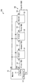
図1に示すように電子制御装置100はマイクロコンピュータの構成要素としてマスタIC10と3つのスレーブIC31〜33を有する。マスタIC10から3つのスレーブIC31〜33それぞれに共通したクロック信号が出力される。これによりマスタIC10と3つのスレーブIC31〜33それぞれは同期処理を行っている。またマスタIC10から3つのスレーブIC31〜33それぞれに共通した同一のチップセレクト信号が出力される。スレーブIC31〜33はこのチップセレクト信号に基づいてマスタIC10から出力される送信フレームの指令信号の受信、および、それに対する応答信号の送信を確定する。より詳しく言えば、スレーブIC31〜33はチップセレクト信号の電圧レベルがLoレベル若しくはHiレベルで一定の場合、信号の送受信の確定を行わない。しかしながらスレーブIC31〜33はチップセレクト信号の電圧レベルがLoレベルからHiレベルに立ち上がると入力されている指令信号の受信を確定する。またスレーブIC31〜33はチップセレクト信号の電圧レベルがHiレベルからLoレベルに立ち下がると応答信号の送信を確定する。Loレベルが第1レベルに相当する。Hiレベルが第2レベルに相当する。
As shown in FIG. 1, the
以下においては表記が煩雑となることを避けるためにクロック信号、チップセレクト信号を、CLK信号、CS信号と示す。またCS信号がLoレベルの期間をCS期間と示す。 In the following description, the clock signal and the chip select signal are referred to as a CLK signal and a CS signal in order to avoid complicated description. A period in which the CS signal is at Lo level is referred to as a CS period.
マスタIC10とスレーブIC31〜33はデイジーチェーン50によって数珠つなぎに連結されている。本実施形態のデイジーチェーン50は第1バス51〜第4バス54を有する。図1ではスレーブIC31〜33の送受信機の記載を省略しているが、マスタIC10の送信機11と受信機12とを明示している。第1バス51はマスタIC10の送信機11の出力ポートと第1スレーブIC31の受信ポートとを接続する。第2バス52は第1スレーブIC31の出力ポートと第2スレーブIC32の受信ポートとを接続する。第3バス53は第2スレーブIC32の出力ポートと第3スレーブIC33の受信ポートとを接続する。そして第4バス54は第3スレーブIC33の出力ポートとマスタIC10の受信機12の受信ポートとを接続する。
The master IC 10 and the
スレーブIC31〜33はCS信号の電圧レベルが一定の場合、CLK信号に同期して入力された送信フレームを通過してそのまま出力する。したがって例えばCS信号がLoレベルのままの場合、マスタIC10が送信フレームを第1バス51に出力すると、その送信フレームはバス51〜54およびスレーブIC31〜33を経てマスタIC10へとかえってくる。
When the voltage level of the CS signal is constant, the
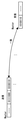
マスタIC10は送信フレームに上記した指令信号の他にダミー信号を含ませる。図2に示すようにマスタIC10はスレーブIC31〜33それぞれに対応する第1指令信号〜第3指令信号(Slave1−Command〜Slave3−Command)を生成する。またマスタIC10はダミー信号(Dummy)を記憶している。
The master IC 10 includes a dummy signal in addition to the command signal described above in the transmission frame. As shown in FIG. 2, the
送信フレームに含まれる第1指令信号〜第3指令信号とダミー信号の順番は定まっている。図2に示すように送信フレームの先頭にダミー信号が位置する。そしてその次から順に第3指令信号、第2指令信号、および、第1指令信号が並ぶ。 The order of the first to third command signals and the dummy signal included in the transmission frame is determined. As shown in FIG. 2, the dummy signal is located at the head of the transmission frame. Then, the third command signal, the second command signal, and the first command signal are arranged in order from the next.
次に、図3および図4に基づいて、マスタIC10とスレーブIC31〜33のシリアル通信を説明する。図3に示すTrans(SO)はマスタIC10の送信レジスタ13と送信フレームを示している。Slave1、Slave2、Slave3は、スレーブIC31〜33の送受信レジスタ34〜36と応答信号および受信信号を示している。またReceive(SI)はマスタIC10の受信レジスタ14と受信フレームを示している。
Next, serial communication between the
図3においては予めスレーブIC31〜33それぞれが応答信号(Slave1−Ans−0〜Slave3−Ans−0)の送信準備を完了しているとする。この応答信号は図3に示すSlave1−Com−1〜Slave3−Com−1に対するものではなく、図示しない直前のCS期間におけるマスタIC10からの指令信号に対するものである。以下においてはこれらスレーブIC31〜33の応答信号を、単に第1〜第3応答信号と示す。
In FIG. 3, it is assumed that each of the
先ず始めにマスタIC10がCS信号をHiレベルからLoレベルに立ち下げる。するとスレーブIC31〜33それぞれは第1〜第3応答信号の送信を確定し、それをデイジーチェーン50に出力する。
First, the
マスタIC10はCS信号を立ち下げるとともに、CLK信号に同期して送信フレームを出力する。この送信フレームはダミー信号を先頭として、それから順に第3指令信号、第2指令信号、および、第1指令信号が並んでいる。これは図3に示すSlave1−Com−1〜Slave3−Com−1、Dummyに相当する。
The
CS信号が立ち下がった直後においては、第1〜第3応答信号、および、送信フレームの先頭に位置するダミー信号は未だデイジーチェーン50に出力されていない。しかしながらそこからCLK信号に同期した時間が経過すると、第3応答信号、第2応答信号、第1応答信号、ダミー信号、第3指令信号、第2指令信号、および、第1指令信号が順次デイジーチェーン50を伝搬していく。
Immediately after the CS signal falls, the first to third response signals and the dummy signal located at the head of the transmission frame have not been output to the
CS信号の立ち下がりからCLK信号に同期した時間が経過して、第3応答信号がマスタIC10に入力されると、第2応答信号が第3スレーブIC33に入力される。第1応答信号が第2スレーブIC32に入力される。ダミー信号が第1スレーブIC31に入力される。
When a time synchronized with the CLK signal elapses from the fall of the CS signal and the third response signal is input to the
そこからさらにCLK信号に同期した時間が進み、第2応答信号がマスタIC10に入力されると、第1応答信号が第3スレーブIC33に入力される。ダミー信号が第2スレーブIC32に入力される。第3指令信号が第1スレーブIC31に入力される。
When the time further synchronized with the CLK signal advances from there and the second response signal is input to the
第1応答信号がマスタIC10に入力されると、ダミー信号が第3スレーブIC33に入力される。第3指令信号が第2スレーブIC32に入力される。第2指令信号が第1スレーブIC31に入力される。
When the first response signal is input to the
最後に、ダミー信号がマスタIC10にかえってくると、第3指令信号が第3スレーブIC33に入力される。第2指令信号が第2スレーブIC32に入力される。第1指令信号が第1スレーブIC31に入力される。この際にマスタIC10はCS信号をLoレベルからHiレベルに立ち上げる。これによりスレーブIC31〜33は入力されている指令信号の受信を確定する。すなわち第1スレーブIC31は第1指令信号の受信を確定する。第2スレーブIC32は第2指令信号の受信を確定する。第3スレーブIC33は第3指令信号の受信を確定する。
Finally, when the dummy signal is returned to the
またマスタIC10はCS信号をLoレベルからHiレベルに立ち上げると、デイジーチェーン50とスレーブIC31〜33を経てかえってきたダミー信号を受信する。マスタIC10はこの受信したダミー信号と、記憶していたダミー信号とを照合する。その照合の結果、図4に示すように2つのダミー信号が一致している場合、マスタIC10はシリアル通信が正常であると判定する。しかしながら図5に示すように2つのダミー信号が不一致の場合、マスタIC10はシリアル通信に異常が生じていると判定する。そしてマスタIC10はシステム機能に応じたフェイルセーフ制御を実施する。例えばマスタIC10はエンジンをフェイルセーフ制御する。
Further, when the
以上が図3に示すSlave1−Com−1〜Slave3−Com−1、Dummyを含む1つの送信フレームを送信した際のマスタIC10とスレーブIC31〜33の挙動である。この後にマスタIC10は図3に示すSlave1−Com−2〜Slave3−Com−2、Dummyを含む送信フレームを出力するが、その際のマスタIC10とスレーブIC31〜33の挙動は上記と同様である。したがって、その記載を省略する。
The above is the behavior of the
なお図5に示すようにダミー信号が不一致となるのは、例えばクロック信号のパルス周期の高速化や、デイジーチェーン50とスレーブIC31〜33の伝搬による遅延のためである。このような遅延を検出するためにも、ダミー信号は1と0とがなるべく連続しない構成としている。またデイジーチェーン50が天絡、地絡、および、オープンとなった場合、デイジーチェーン50とスレーブIC31〜33を経てかえってきたダミー信号は全て1若しくは全て0となる。これを検出するためにも、例えば図4に示すように送信するダミー信号は10100110などのように1と0を組み合わせたパターンとしている。
The reason why the dummy signals do not match as shown in FIG. 5 is due to, for example, an increase in the pulse period of the clock signal and a delay due to propagation of the
次に、本実施形態に係る電子制御装置100の作用効果を説明する。上記したように送信フレームにダミー信号を含ませる。これによればマスタIC10が1度送信フレームを出力するだけで、シリアル通信の異常を判定することができる。具体的に言えばマスタIC10からスレーブIC31〜33へ信号がズレること無く送受信が完了できているか否かを判定することができる。換言すれば1度のCS期間で信号のズレを判定することができる。従来、マスタICが1度送信フレームを出力した後、送信フレームに含まれる指令信号に応じたスレーブICからの応答信号をマスタICが受信することによってシリアル通信の異常を判定する。この比較構成の場合、シリアル通信の異常を検出するためには最短でも2度のCS期間を必要とする。したがってこの比較構成と比べて、シリアル通信の異常を早く検出することができる。
Next, functions and effects of the
以上、本発明の好ましい実施形態について説明したが、本発明は上記した実施形態になんら制限されることなく、本発明の主旨を逸脱しない範囲において、種々変形して実施することが可能である。 The preferred embodiments of the present invention have been described above. However, the present invention is not limited to the above-described embodiments, and various modifications can be made without departing from the spirit of the present invention.
本実施形態では電子制御装置100はエンジンECUである例を示した。しかしながら電子制御装置100の適用としては上記例に限定されず、車両に搭載される電子制御装置であれば適宜採用することができる。例えばバッテリECUやトランスミッションECUなどに採用することもできる。
In the present embodiment, an example in which the
本実施形態では電子制御装置100が3つのスレーブIC31〜33を有する例を示した。しかしながらスレーブICの数としては上記例に限定されず、複数であればよい。すなわち、電子制御装置100が2つのスレーブICを有してもよいし、3つ以上のスレーブICを有してもよい。
In this embodiment, the example which the
10…マスタIC
31…第1スレーブIC
32…第2スレーブIC
33…第3スレーブIC
50…デイジーチェーン
100…電子制御装置
10 ... Master IC
31 ... 1st slave IC
32 ... Second slave IC
33 ... Third slave IC
50 ...
Claims (5)
前記マスタICは、
前記シリアル通信の異常を検出するためのダミー信号を記憶しており、
複数の前記スレーブICへの指令信号の他に前記ダミー信号を含ませた送信フレームを前記デイジーチェーンに出力し、
記憶していた前記ダミー信号と、複数の前記スレーブICおよび前記デイジーチェーンを経てかえってきた前記ダミー信号とを照合し、その照合結果が不一致の場合、前記シリアル通信に異常が生じていると判定する電子制御装置。 An electronic control unit in which a master IC (10) and a plurality of slave ICs (31 to 33) are connected in a daisy chain (50) and serial communication is performed between the master IC and the plurality of slave ICs. ,
The master IC is
A dummy signal for detecting an abnormality of the serial communication is stored,
Outputting a transmission frame including the dummy signal in addition to the command signals to the plurality of slave ICs to the daisy chain;
The stored dummy signal and the plurality of slave ICs and the dummy signal returned through the daisy chain are collated, and if the collation result does not match, it is determined that an abnormality has occurred in the serial communication. Electronic control device.
複数の前記スレーブICは前記チップセレクト信号の電圧レベルが第1レベルの場合に前記送信フレームを通過させて前記デイジーチェーンに出力し、前記チップセレクト信号の電圧レベルが前記第1レベルから第2レベルに変化すると入力されている前記送信フレームを受信しており、
前記マスタICは、
前記チップセレクト信号を前記第1レベルにしている間に前記送信フレームを前記デイジーチェーンに出力し、
前記送信フレームを出力し終えると前記チップセレクト信号を前記第1レベルから前記第2レベルに変化させる請求項2に記載の電子制御装置。 The master IC outputs the same chip select signal to the plurality of slave ICs,
The plurality of slave ICs pass the transmission frame and output to the daisy chain when the voltage level of the chip select signal is the first level, and the voltage level of the chip select signal is changed from the first level to the second level. When the transmission frame is changed to the received transmission frame is received,
The master IC is
Outputting the transmission frame to the daisy chain while the chip select signal is at the first level;
The electronic control device according to claim 2, wherein when the transmission frame is output, the chip select signal is changed from the first level to the second level.
Priority Applications (1)
| Application Number | Priority Date | Filing Date | Title |
|---|---|---|---|
| JP2016004602A JP6597325B2 (en) | 2016-01-13 | 2016-01-13 | Electronic control unit |
Applications Claiming Priority (1)
| Application Number | Priority Date | Filing Date | Title |
|---|---|---|---|
| JP2016004602A JP6597325B2 (en) | 2016-01-13 | 2016-01-13 | Electronic control unit |
Publications (2)
| Publication Number | Publication Date |
|---|---|
| JP2017126858A true JP2017126858A (en) | 2017-07-20 |
| JP6597325B2 JP6597325B2 (en) | 2019-10-30 |
Family
ID=59364463
Family Applications (1)
| Application Number | Title | Priority Date | Filing Date |
|---|---|---|---|
| JP2016004602A Active JP6597325B2 (en) | 2016-01-13 | 2016-01-13 | Electronic control unit |
Country Status (1)
| Country | Link |
|---|---|
| JP (1) | JP6597325B2 (en) |
Cited By (1)
| Publication number | Priority date | Publication date | Assignee | Title |
|---|---|---|---|---|
| US11449381B2 (en) | 2017-12-21 | 2022-09-20 | Lg Energy Solution, Ltd. | Apparatus and method for diagnosing communication fault |
Citations (2)
| Publication number | Priority date | Publication date | Assignee | Title |
|---|---|---|---|---|
| JPS5538715A (en) * | 1978-09-11 | 1980-03-18 | Hitachi Ltd | Fault detection system |
| JPS59101945A (en) * | 1982-12-02 | 1984-06-12 | Fujitsu Ltd | Data highway diagnosing system |
-
2016
- 2016-01-13 JP JP2016004602A patent/JP6597325B2/en active Active
Patent Citations (2)
| Publication number | Priority date | Publication date | Assignee | Title |
|---|---|---|---|---|
| JPS5538715A (en) * | 1978-09-11 | 1980-03-18 | Hitachi Ltd | Fault detection system |
| JPS59101945A (en) * | 1982-12-02 | 1984-06-12 | Fujitsu Ltd | Data highway diagnosing system |
Cited By (1)
| Publication number | Priority date | Publication date | Assignee | Title |
|---|---|---|---|---|
| US11449381B2 (en) | 2017-12-21 | 2022-09-20 | Lg Energy Solution, Ltd. | Apparatus and method for diagnosing communication fault |
Also Published As
| Publication number | Publication date |
|---|---|
| JP6597325B2 (en) | 2019-10-30 |
Similar Documents
| Publication | Publication Date | Title |
|---|---|---|
| JP5193067B2 (en) | Multi-sensor circuit for automatic address acquisition | |
| JP5393932B1 (en) | Data processing apparatus and communication system | |
| US9783138B2 (en) | Vehicle control device | |
| US9515906B2 (en) | Transceiver integrated circuit device and method of operation thereof | |
| JP6207987B2 (en) | In-vehicle electronic control unit | |
| US11394726B2 (en) | Method and apparatus for transmitting a message sequence over a data bus and method and apparatus for detecting an attack on a message sequence thus transmitted | |
| JP7119437B2 (en) | Vehicle master electronic controller, vehicle slave electronic controller, vehicle log collection system, and vehicle log collection program | |
| JP2007034910A (en) | Multi-cpu system and scheduler | |
| JP4465905B2 (en) | Electronic control unit | |
| JP6597325B2 (en) | Electronic control unit | |
| US10715796B2 (en) | Method and device for monitoring an image sensor | |
| JP2009302783A (en) | Failure detecting method and failure detection system of communication network | |
| US9065560B2 (en) | Method for checking the operation of a PSI5 reception unit in a motor vehicle controller, and corresponding PSI5 reception unit | |
| JP2003285700A (en) | Failure-diagnosing device for vehicle | |
| EP3623228B1 (en) | A vehicle safety system and a method of controlling a vehicle safety system | |
| JP2008082959A (en) | Ecu function inspecting apparatus | |
| JP3459075B2 (en) | Synchronous serial bus method | |
| JP2001334908A (en) | Vehicular occupant protection system | |
| KR101826779B1 (en) | An apparatus and method for testing control logic of application specific integrated circuit | |
| JP2018151921A (en) | Electronic control device | |
| JP3057539B2 (en) | Communication emulator device | |
| JP2009005160A (en) | Error generation device | |
| CN101795217A (en) | Two diagnosis that communication network is synchronous of the data handling system of electronics | |
| JP5545125B2 (en) | Communication device | |
| JP2023030929A (en) | Primary check system |
Legal Events
| Date | Code | Title | Description |
|---|---|---|---|
| A621 | Written request for application examination |
Free format text: JAPANESE INTERMEDIATE CODE: A621 Effective date: 20180413 |
|
| A977 | Report on retrieval |
Free format text: JAPANESE INTERMEDIATE CODE: A971007 Effective date: 20190206 |
|
| A131 | Notification of reasons for refusal |
Free format text: JAPANESE INTERMEDIATE CODE: A131 Effective date: 20190312 |
|
| A521 | Request for written amendment filed |
Free format text: JAPANESE INTERMEDIATE CODE: A523 Effective date: 20190419 |
|
| TRDD | Decision of grant or rejection written | ||
| A01 | Written decision to grant a patent or to grant a registration (utility model) |
Free format text: JAPANESE INTERMEDIATE CODE: A01 Effective date: 20190903 |
|
| A61 | First payment of annual fees (during grant procedure) |
Free format text: JAPANESE INTERMEDIATE CODE: A61 Effective date: 20190916 |
|
| R151 | Written notification of patent or utility model registration |
Ref document number: 6597325 Country of ref document: JP Free format text: JAPANESE INTERMEDIATE CODE: R151 |
|
| R250 | Receipt of annual fees |
Free format text: JAPANESE INTERMEDIATE CODE: R250 |
|
| R250 | Receipt of annual fees |
Free format text: JAPANESE INTERMEDIATE CODE: R250 |