JP2017126544A - Non-arc current switching device - Google Patents
Non-arc current switching device Download PDFInfo
- Publication number
- JP2017126544A JP2017126544A JP2016013814A JP2016013814A JP2017126544A JP 2017126544 A JP2017126544 A JP 2017126544A JP 2016013814 A JP2016013814 A JP 2016013814A JP 2016013814 A JP2016013814 A JP 2016013814A JP 2017126544 A JP2017126544 A JP 2017126544A
- Authority
- JP
- Japan
- Prior art keywords
- contact
- switch
- gate
- mosfet
- current
- Prior art date
- Legal status (The legal status is an assumption and is not a legal conclusion. Google has not performed a legal analysis and makes no representation as to the accuracy of the status listed.)
- Granted
Links
- 239000004065 semiconductor Substances 0.000 claims abstract description 67
- 229910052751 metal Inorganic materials 0.000 claims abstract description 28
- 239000002184 metal Substances 0.000 claims abstract description 28
- 230000000694 effects Effects 0.000 claims abstract description 10
- 230000010354 integration Effects 0.000 claims abstract description 6
- 239000003990 capacitor Substances 0.000 claims description 14
- 230000003287 optical effect Effects 0.000 claims description 11
- 230000001172 regenerating effect Effects 0.000 claims description 9
- 239000006096 absorbing agent Substances 0.000 claims description 4
- 230000008878 coupling Effects 0.000 claims description 4
- 238000010168 coupling process Methods 0.000 claims description 4
- 238000005859 coupling reaction Methods 0.000 claims description 4
- 238000004891 communication Methods 0.000 claims description 3
- 230000007423 decrease Effects 0.000 claims description 3
- 238000010586 diagram Methods 0.000 description 13
- 230000002441 reversible effect Effects 0.000 description 9
- 244000145845 chattering Species 0.000 description 8
- HBMJWWWQQXIZIP-UHFFFAOYSA-N silicon carbide Chemical compound [Si+]#[C-] HBMJWWWQQXIZIP-UHFFFAOYSA-N 0.000 description 7
- 229910010271 silicon carbide Inorganic materials 0.000 description 7
- 238000004088 simulation Methods 0.000 description 6
- 230000000903 blocking effect Effects 0.000 description 5
- 238000002474 experimental method Methods 0.000 description 4
- 238000012795 verification Methods 0.000 description 4
- 230000008901 benefit Effects 0.000 description 3
- 238000009413 insulation Methods 0.000 description 3
- 235000014676 Phragmites communis Nutrition 0.000 description 2
- XUIMIQQOPSSXEZ-UHFFFAOYSA-N Silicon Chemical compound [Si] XUIMIQQOPSSXEZ-UHFFFAOYSA-N 0.000 description 2
- 230000002457 bidirectional effect Effects 0.000 description 2
- 238000004364 calculation method Methods 0.000 description 2
- 238000001816 cooling Methods 0.000 description 2
- 230000020169 heat generation Effects 0.000 description 2
- 230000006872 improvement Effects 0.000 description 2
- 230000007257 malfunction Effects 0.000 description 2
- 239000007769 metal material Substances 0.000 description 2
- 230000003071 parasitic effect Effects 0.000 description 2
- 229910052710 silicon Inorganic materials 0.000 description 2
- 239000010703 silicon Substances 0.000 description 2
- 230000001052 transient effect Effects 0.000 description 2
- 238000010521 absorption reaction Methods 0.000 description 1
- 230000008033 biological extinction Effects 0.000 description 1
- 230000015556 catabolic process Effects 0.000 description 1
- 230000008859 change Effects 0.000 description 1
- 230000003247 decreasing effect Effects 0.000 description 1
- 230000003111 delayed effect Effects 0.000 description 1
- 230000005669 field effect Effects 0.000 description 1
- 230000005389 magnetism Effects 0.000 description 1
- 239000000463 material Substances 0.000 description 1
- 230000007246 mechanism Effects 0.000 description 1
- QSHDDOUJBYECFT-UHFFFAOYSA-N mercury Chemical compound [Hg] QSHDDOUJBYECFT-UHFFFAOYSA-N 0.000 description 1
- 229910052753 mercury Inorganic materials 0.000 description 1
- 229910044991 metal oxide Inorganic materials 0.000 description 1
- 150000004706 metal oxides Chemical class 0.000 description 1
- 238000000034 method Methods 0.000 description 1
- 230000007935 neutral effect Effects 0.000 description 1
- 230000007420 reactivation Effects 0.000 description 1
- 230000004044 response Effects 0.000 description 1
- 230000000630 rising effect Effects 0.000 description 1
- 229920006395 saturated elastomer Polymers 0.000 description 1
- 230000002459 sustained effect Effects 0.000 description 1
- 230000001360 synchronised effect Effects 0.000 description 1
Images


Abstract
Description
本発明は、電力系のスイッチ装置に関し、直流または交流電流の、電力系統、鉄道、電気自動車、配電の施設、屋内配線等の電力を扱うにおいて必要な電流の開閉器に属し、金属接点による直流電流の遮断では発生するアークが持続することで、数十V以上数A以上の遮断は容易ではない。直流電流を遮断するにアークを発生すること無く遮断可能になるように、半導体スイッチと、導通損失の低い金属接点スイッチとで構成される無アーク電流開閉装置に関する。 The present invention relates to a switch device for a power system, and belongs to a switch of a current necessary for handling power of a direct current or alternating current, such as a power system, a railway, an electric vehicle, a distribution facility, an indoor wiring, etc. When the current is interrupted, the generated arc is sustained, so that it is not easy to interrupt several tens V or more and several A or more. The present invention relates to an arc-free current switching device composed of a semiconductor switch and a metal contact switch with low conduction loss so that it can be interrupted without generating an arc when interrupting a direct current.
半導体スイッチの進歩により、高電圧・大電流が高速に遮断可能になった。しかし、アークの消滅による遮断は数μ秒であったが、MOSFETはより速く、数10ナノ秒でオン、オフするので、インダクタンスのある回路の電流を遮断すると、高い再起電圧が発生して、バリスタやなどのスナバ回路を必要とするなど、保護回路が必要である。高速すぎる遮断は、返ってそのために開閉サージが増している。 Advances in semiconductor switches have made it possible to shut off high voltages and large currents at high speed. However, the interruption due to the extinction of the arc was several microseconds, but the MOSFET is faster and turns on and off in several tens of nanoseconds, so when the current of the circuit with inductance is interrupted, a high regenerative voltage is generated, A protection circuit is necessary, such as a snubber circuit such as a varistor. An interruption that is too fast will return and therefore increase the switching surge.
一方、直流電流の遮断を金属接点の開極で行うと電流が遮断されずに連続する。開極時に発生するアークにより通電し、アークを消滅させなければ電流は遮断できない。アークを消弧するにはアーク長を磁気などで長くし、冷却して消弧するが、この間、電極が消耗して接点の寿命が短くなってしまう。 On the other hand, when the direct current is interrupted by opening the metal contact, the current continues without being interrupted. The current cannot be cut off unless the arc is extinguished by applying an electric current by the arc generated at the time of opening. In order to extinguish the arc, the arc length is increased by magnetism or the like, and the arc is extinguished by cooling, but during this time, the electrode is consumed and the contact life is shortened.
近年シリコン・カーバイド系の半導体が実用化されて、MOSFET(Metal Oxide Semiconductor Field Effect Transistor)で1000Vを越える高耐電圧の半導体スイッチが実用化されている。この高耐圧の半導体スイッチを使って高電圧の直流電力系の開閉、遮断スイッチが提供できるようになった。しかし、まだまだ、半導体スイッチの通電損は金属接点より大きく数10W程度あるので、半導体スイッチの冷却装置が必要となり、大型になってしまうのが欠点である。そこで、両方の利点を組み合わせて、通電は金属接点で、遮断時のみ半導体スイッチで通電、遮断する無アーク開閉器、遮断器が望まれている。 In recent years, silicon carbide semiconductors have been put into practical use, and semiconductor switches having a high withstand voltage exceeding 1000 V have been put into practical use in MOSFETs (Metal Oxide Semiconductor Field Effect Transistors). Using this high withstand voltage semiconductor switch, it is now possible to provide an open / close switch for a high voltage DC power system. However, since the current loss of the semiconductor switch is about several tens of watts larger than that of the metal contact point, a cooling device for the semiconductor switch is necessary, and the semiconductor switch becomes large. Therefore, by combining both advantages, there is a demand for an arc-free switch and a circuit breaker that are energized by a metal contact and energized and interrupted by a semiconductor switch only at the time of interruption.
本発明は特願2015−078094に記載した金属接点と半導体スイッチの並列接続による無アーク開閉器をさらに効果を増し、応用範囲を広げるようにする改良に関するものである。 The present invention relates to an improvement in which the arc-free switch by parallel connection of a metal contact and a semiconductor switch described in Japanese Patent Application No. 2015-078094 is further improved in effect and widened in application range.
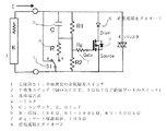
特許文献1に記載の発明の中で、先行特許中の図6では、機械接点と半導体スイッチの並列接続であって、通電は金属接点で行い、金属接点の低オン抵抗で発熱はない。電流を遮断する時は、半導体スイッチに転流して、半導体スイッチのゲート制御によって高速に遮断する。 Among the inventions described in
図1は特許文献1に記載の図6の直流開閉器であるが、これには2つの特徴がある。第一の特徴はゲート回路である。直流をMOSFET、IGBT、(Insulated Gate By−polar Transistor)などの絶縁ゲートの半導体スイッチでオン・オフするが、半導体スイッチのゲートをON状態にする電圧を半導体スイッチに印加されるドレイン電圧を使っているためゲート駆動電源が不要である。MOSFETのドレインの電圧を高抵抗100kΩ以上の抵抗でゲートに接続することによって、MOSFETの閾値(Vth)で電流が流れ出し、Vth+オン抵抗の電圧以上にはならない。Vthは3V程度である。 並列に接続されている通電接点である金属接点ではアークの発生する最低電圧は10V程度であるので、アークは発生しない。接点電流は無アークで半導体スイッチに転流する。 FIG. 1 shows the DC switch of FIG. 6 described in
特許文献1に記載の発明では、ドレイン電圧でゲートをオンしているのでオン電圧はVth以下にはならない。ゲートに十分大きな電圧を与えて、飽和領域で駆動できればオン電圧は電流×オン抵抗になって、Vthより小さくなる。これにより発熱が下がり、さらに大きな過電流耐量を利用できるようになる。 In the invention described in
先行特許のもう一つの新規なところは、1極双投スイッチのa接点、b接点を利用して半導体スイッチのゲート信号を制御することを特徴としている。しかし、a接点は、大電流を通電するため、低抵抗である必要があるが、b接点はゲート電圧の制御のための接点であるから電流容量はa接点に比べてわずかである。また、b接点がオンするとMOSFETが遮断するがその遮断スピードが速いので再起電圧も急峻でサージ電圧が発生する。b接点のオン時にチャタリングを起こすと、それに伴ってサージ電圧を多数回、発生する。b接点はチャタリングの起こしにくい金属材料の接点が望ましい。チャタリングの起こさない、接触不良を起こさないスイッチとして水銀スイッチがあるが、要するに柔らかい金属材料がよい。b接点に代わるゲート、ソース間を低抵抗で短絡するスイッチであれば、連動して動作する補助接点、絶縁光カップラ、リードリレーなども可能である。 Another novel part of the prior patent is characterized in that the gate signal of the semiconductor switch is controlled using the a-contact and b-contact of the one-pole double-throw switch. However, the a contact is required to have a low resistance in order to pass a large current. However, since the b contact is a contact for controlling the gate voltage, the current capacity is small compared to the a contact. Further, when the b-contact is turned on, the MOSFET is cut off, but since the cut-off speed is fast, the regenerative voltage is steep and a surge voltage is generated. When chattering occurs when the b-contact is on, a surge voltage is generated many times. The b contact is preferably a contact made of a metal material that hardly causes chattering. There is a mercury switch as a switch that does not cause chattering and does not cause poor contact. In short, a soft metal material is preferable. As long as it is a switch that short-circuits the gate and source instead of the b contact with a low resistance, an auxiliary contact, an insulated optical coupler, a reed relay, and the like that operate in conjunction with each other are possible.
本発明は、かかる先に出願された発明をさらに電流の開閉器、遮断器への応用に鑑みなされたものであり、金属接点の問題点を解決し、また半導体スイッチの発熱などの問題点を解決して交流・直流電源を安全かつ確実に短絡、開放、遮断することが可能な開閉器、遮断器を提供することを目的とする。 The present invention has been made in view of the application of the previously filed invention to a current switch and circuit breaker, solves the problem of metal contacts, and solves problems such as heat generation of semiconductor switches. It is an object of the present invention to provide a switch and a circuit breaker that can solve the problem by short-circuiting, opening, and interrupting an AC / DC power supply safely and reliably.
上記目的を達成するために、金属接点と並列に半導体スイッチを接続される、直流電流を開閉させるスイッチは、一つのMOSFETと、そのMOSFETのドレインを金属接点のa接点に接続し、MOSFETのソースを金属接点のコモン電極に接続し、ドレイン、ゲート間に接続された抵抗器と、前記MOSFETのソース、ゲートをb接点によって短絡するスイッチを備えたことを特徴とする特許文献1に記載の発明の図6の機械接点と半導体スイッチの並列接続した無アーク遮断スイッチを基礎にさらに以下のように1から5にあげる改良をすることにより利用範囲を広げる。 In order to achieve the above object, a semiconductor switch is connected in parallel with a metal contact, and a switch for opening and closing a direct current has one MOSFET and a drain of the MOSFET connected to a contact of the metal contact, and the source of the MOSFET Is connected to a common electrode of a metal contact, and includes a resistor connected between a drain and a gate, and a switch for short-circuiting the source and gate of the MOSFET by a b contact. Based on the arc-less cut-off switch in which the mechanical contact and the semiconductor switch in FIG. 6 are connected in parallel, the range of use is expanded by further improving from 1 to 5 as follows.
1. 半導体スイッチのゲートにゲートを飽和領域の電圧を与えて、オン抵抗をさらに 小さくするために、絶縁した電源を用意してゲートを飽和状態のオンにして、半 導体をオフにする時、b接点のオンで絶縁電源をゼロにするがゲート抵抗Rgと ドレイン・ゲート間の寄生容量によるミラー積分効果で再起電圧を遅く上昇させ る。絶縁電源には太陽電池、絶縁DC電源、充電2次電池、長寿命な電池などが ある。 1. When applying a voltage in the saturation region to the gate of the semiconductor switch to further reduce the on-resistance, an isolated power supply is prepared, the gate is turned on in a saturated state, and the semiconductor is turned off. When the power is turned on, the insulated power supply is made zero, but the regenerative voltage is slowly increased by the Miller integration effect due to the gate resistance Rg and the parasitic capacitance between the drain and gate. Insulated power sources include solar cells, insulated DC power sources, rechargeable secondary batteries, and long-life batteries.
2. b接点のオンで半導体スイッチをオフする際に、b接点を直接には使わず、光結 合スイッチなどの組み合わせでゲート電圧を短絡する。電磁リレーでは、リレー 駆動電源のオン、オフを利用して光結合スイッチやリードリレーなどでb接点の 代わりとなるようにタイマーで然るべき時間遅れを設けて駆動してもよい。 2. When the semiconductor switch is turned off by turning on the b contact, the gate voltage is short-circuited by a combination of an optical coupling switch and the like without using the b contact directly. The electromagnetic relay may be driven with a proper time delay using a timer so that it can be used as an alternative to the b-contact with an optical coupling switch or a reed relay by using on / off of the relay drive power supply.
3. b接点の信号がチャタリングを起こす場合の対策として、防止する回路を付加す る。併せて、近年の半導体スイッチの遮断スピードが速いので、高周波のノイズ を発生し、ノイズによる誤動作を発生する可能性がある。半導体スイッチの遮断 スピードを遅くする回路、再起電圧制御回路を付加する。 3. Add a circuit to prevent b chattering of the contact signal. In addition, the recent semiconductor switch shutoff speed is fast, which may cause high-frequency noise and malfunction due to noise. Add a circuit that slows down the semiconductor switch and a regenerative voltage control circuit.
4. 金属接点のa接点とドレインの間にダイオードを入れて、逆電流阻止構造の直流 開閉器にする。これは負荷側に電圧が残っている場合、遮断後に電流が逆流する 可能性を除くために必要である。MOSFETなど半導体スイッチとして逆導通 型スイッチを用いる場合、逆阻止能力は必要なことである。また、ダイオードの 順方向電圧降下、約1.2Vが加わるが、MOSFETの電圧降下は下がるので 大電流を流すことができる。図11のMOSFETの損失をシミュレーションで 求めたが損失はI/3になっている。 4). A diode is inserted between the metal contact a and the drain to form a reverse current blocking DC switch. This is necessary to eliminate the possibility of reverse current flow after interruption when voltage remains on the load side. When a reverse conduction type switch is used as a semiconductor switch such as a MOSFET, a reverse blocking capability is necessary. In addition, although a forward voltage drop of about 1.2 V is applied to the diode, a large current can flow because the voltage drop of the MOSFET is lowered. Although the loss of the MOSFET in FIG. 11 was obtained by simulation, the loss was I / 3.
5. 交流用の開閉器も多頻度開閉を行うと、アークによる電極消耗が開閉器の寿命と なる。アークを最小限にするか、できれば無アークで遮断するのが望ましい。3 相交流の電流瞬断は3相同時になるように、連動する補助接点のb接点からのオ ン信号で三相の3つの半導体スイッチを同時にオフする。この場合、半導体スイ ッチはトライアックでも良い。電流のゼロ点でソフトにオフする利点はある。ま た交流電流遮断でも直流分が重畳する場合があり、電流ゼロ点が無い、所謂ゼロ ミス現象時は、直流遮断と変わらないので、トライアックでは無く遮断性能のあ るMOSFETを主接点と連動する補助b接点のオンで3相とも同時に遮断を行 うのが理想である。 5. If an AC switch is also opened and closed frequently, electrode consumption due to arcing will reach the life of the switch. It is desirable to minimize arcing or, if possible, shut off without arcing. The three-phase three semiconductor switches are turned off at the same time by the ON signal from the b contact of the interlocking auxiliary contact so that the instantaneous interruption of the current of the three-phase alternating current occurs at the same time for the three phases. In this case, the semiconductor switch may be a triac. There is an advantage of soft-off at the zero point of the current. In addition, the DC component may be superimposed even when AC current is interrupted, and when there is no zero current point, the so-called zero-miss phenomenon, it is not different from DC interrupt, so a MOSFET with interrupting performance is linked to the main contact instead of a triac. Ideally, all three phases should be shut off simultaneously when the auxiliary b-contact is on.
半導体スイッチのゲート駆動に特別な電源を必要としない構成は先の特許文献1、2に記載の発明の特徴で簡単に手動トグルスイッチへも応用できた。さらに進めて、電磁リレーや制御リレーの応用、インターネットなどの通信系統との情報交換により、電源のオン、オフを行う電流スイッチを制御管理することができる。この場合、制御電源があるのでそれを利用した絶縁ゲート駆動回路は半導体スイッチのゲートに十分な電圧を印加して確実に飽和状態のオンにして、先の特許文献1、2の場合より多くの電流を通電できる。 A configuration that does not require a special power source for driving the gate of the semiconductor switch can be easily applied to a manual toggle switch due to the features of the inventions described in the
無アークで金属接点の遮断器を開極し、その後、十分な絶縁耐圧を持つために、b接点のオン信号を用いるのは金属接点が開極し開極距離がある距離になったことを確実に示す信号であるからである。金属接点の動作を確実に捉える信号である。開極距離が確保されてから半導体スイッチが電流遮断するので、手動の開極をおこなう場合、開極スピードが、一定しないがその場合もb接点のオンを持って遮断するので、多様な開閉スイッチでの応用が可能である。b接点をそれにかわる同期タイミングを得られるスイッチであれば、小電流の弱電圧のスイッチ、例えばマイクロスイッチ、リミットスイッチで代用できる。弱電流用の接点を持つb接点を主接点と連動させればよい。 In order to have a metal contact breaker open without arc and then have sufficient withstand voltage, the ON signal of b contact is used when the metal contact is opened and the opening distance is a certain distance. This is because the signal is surely shown. This signal reliably captures the operation of metal contacts. Since the semiconductor switch cuts off the current after the opening distance is secured, when opening manually, the opening speed is not constant, but even in that case, the contact is turned off with the b contact ON, so various open / close switches Application in is possible. As long as the switch can obtain the synchronous timing for the b contact, it can be replaced by a small current weak voltage switch such as a micro switch or a limit switch. The b contact having the contact for weak current may be linked with the main contact.
このことによって、例えば電磁駆動のスイッチでは開極スピードが従来はアーク時間を最小にするため、高速な開極動作が必要であったが、それは、遅くても確実に動作する接点電極開閉装置であればよい。そのことで電極を駆動する機構が改良されて、より小型、省エネ、低騒音の新しい電磁開閉器が可能になる。 For this reason, for example, in an electromagnetically driven switch, the opening speed has conventionally required a high speed opening operation in order to minimize the arc time, but this is a contact electrode switching device that operates reliably even at a low speed. I just need it. As a result, the mechanism for driving the electrode is improved, and a new electromagnetic switch with smaller size, energy saving, and low noise becomes possible.
〔第1実施形態:図2〕
以下、本発明の実施形態について図面を参照しつつ詳細に説明する。
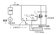
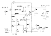
半導体スイッチのゲート電圧に十分高いゲート飽和電圧を与えてオン抵抗を最小にするために、絶縁した電源を付加してゲートをオンし、b接点のオンでゲート電圧をゼロ近くにする。図2は、本発明に係る直流電源の開閉スイッチの第1実施形態を示す回路図である。[First Embodiment: FIG. 2]
Hereinafter, embodiments of the present invention will be described in detail with reference to the drawings.
In order to give a sufficiently high gate saturation voltage to the gate voltage of the semiconductor switch to minimize the on-resistance, an insulated power supply is added to turn on the gate, and when the b-contact is turned on, the gate voltage is made close to zero. FIG. 2 is a circuit diagram showing a first embodiment of the open / close switch of the DC power supply according to the present invention.
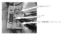
図2において、絶縁された直流電圧源は、小型の太陽電池モジュール(7V−1mA)を使った図3の実証実験の例として説明するが、MOSFETを飽和領域で完全オンするに必要なゲート電圧が発生する。MOSFETのゲートは高い絶縁性能を持つので、ゲート駆動電流はほとんど流れない、したがって、ゲートが単極双投のトグルスイッチのb接点で短絡されない限り、MOSFETは常にON状態である。図4の実験波形によれば、接点電流の流れている金属接点a接点が開極すると、接点の電流は停止し、MOSFETに流れて、接点間はアークの発生に必要な10Vにならないので無アークで電流は半導体スイッチに転流する。双投スイッチの構造から、a接点が開極してから、バウンスする時間後に、コモン電極はb接点に接触する。絶縁DC電源の電圧をb接点がゲート抵抗Rgで短絡すると半導体スイッチはオフされ、再起電圧がミラー積分効果(ブート・ストラップ効果ともいう)でRgと寄生容量で決まる時定数で上昇するが、バリスタで抑えられている。絶縁DC電源が太陽電池である場合、好都合である。太陽電池は、弱くても光があれば無負荷解放電圧が現れ、MOSFETを飽和領域まで駆動できるし、短絡しても定電流電源であるので接点の電流はわずかである。 In FIG. 2, the insulated DC voltage source is described as an example of the demonstration experiment of FIG. 3 using a small solar cell module (7V-1 mA), but the gate voltage required to completely turn on the MOSFET in the saturation region. Will occur. Since the gate of the MOSFET has high insulation performance, almost no gate drive current flows. Therefore, unless the gate is short-circuited at the b-contact of the single-pole double-throw toggle switch, the MOSFET is always in the ON state. According to the experimental waveform of FIG. 4, when the metal contact a contact through which the contact current flows is opened, the contact current stops and flows through the MOSFET, so that the voltage between the contacts does not become 10 V necessary for generating an arc. The electric current is commutated to the semiconductor switch by the arc. Due to the structure of the double throw switch, the common electrode contacts the b contact after the bounce time after the contact a opens. When the voltage of the isolated DC power supply is short-circuited by the gate resistor Rg at the b-contact, the semiconductor switch is turned off, and the regenerated voltage rises with a time constant determined by Rg and parasitic capacitance due to Miller integration effect (also called boot strap effect). It is suppressed by. It is advantageous if the isolated DC power source is a solar cell. Even if the solar cell is weak, if there is light, a no-load release voltage appears, and the MOSFET can be driven to the saturation region.
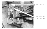
ゲート用電圧源はコンデンサや、充電できる2次電池に置き換えても良いし、MOSFET用のゲート駆動用絶縁電源を用いてもよい。シリコン・カーバイドのMOSFETであっても、飽和領域まで駆動する15V程度まで発生する絶縁電源であれば電流容量は問わない。前述の太陽電池と発光素子を組み込んだ出力電圧7Vの光カップラ、TLP3905は小型でよい。2次出力を2段に直列にすれば15Vの絶縁電源になる。ゲート電源の応答スピードは遅くてもa接点からb接点へのバウンス時間は数mSかかるのでこれに対して十分早ければ問題ない。また、絶縁電圧源を2次電池にして、開閉装置がオフ時の極間電圧で充電される、または電源から絶縁して充電することができる電気2重層キャパシターであっても可能である。図5は実施例1の絶縁電源として、フォトカプラ、赤外LED+フォトダイオード:TLP3905を使った場合の原理検証実験の外観写真である。 The gate voltage source may be replaced with a capacitor or a rechargeable secondary battery, or an insulated power source for gate drive for MOSFET may be used. Even in the case of a silicon carbide MOSFET, the current capacity is not limited as long as it is an insulated power source that generates up to about 15 V that is driven to the saturation region. The TLP3905, an optical coupler with an output voltage of 7 V incorporating the above-described solar cell and light emitting element, may be small. If the secondary output is serially arranged in two stages, an insulated power supply of 15V is obtained. Even if the response speed of the gate power supply is slow, the bounce time from the a-contact to the b-contact takes several mS. It is also possible to use an electric double layer capacitor in which the insulation voltage source is a secondary battery and the switchgear is charged with the voltage between the electrodes when it is off, or can be charged while being insulated from the power source. FIG. 5 is an appearance photograph of a principle verification experiment in the case where a photocoupler, an infrared LED + photodiode: TLP3905 is used as the insulated power source of the first embodiment.
図2において、ZnOバリスタ(ZNRとも呼ばれる過電圧保護用非線形抵抗)をMOSFETの過電圧保護のために接続している。これは遮断する直流回路に大きなインダクタンスがある場合、その磁気エネルギーを吸収するので必要に応じて付加する。バリスタのエネルギー吸収能力は、半導体スイッチより10倍以上大きい。 In FIG. 2, a ZnO varistor (non-linear resistance for overvoltage protection, also called ZNR) is connected for overvoltage protection of the MOSFET. If the DC circuit to be cut off has a large inductance, the magnetic energy is absorbed and added as necessary. The varistor's energy absorption capacity is more than 10 times greater than that of a semiconductor switch.
図6は、長寿命の電池をゲート電源として遮断時、無アーク遮断が可能な直流開閉器である。主接点a接点と連動する接点、例えば補助接点、または2極双投トグルスイッチの場合は、もう一方のa接点を使ってゲートに電荷を蓄積して、b接点のオンでMOSFETのゲートの電荷を消滅するまで導通しているので、主接点a接点の開ではアークは発生しない。この連動するb接点回路を用いるとゲート電源はMOSFETのゲートをチャージ・アップするのみでよいので、絶縁された電源が長寿命の電池を使用することができる。この電池の代わりにキャパシターにして、別電源で充電する方法をとっても良い。併せて、CとRでゲート回路を構成すればMOSFETのドレイン電圧の変化率を抑えることができ、ノイズの少ない開閉が可能になる。 FIG. 6 shows a DC switch capable of arc-free interruption when a long-life battery is used as a gate power supply. In the case of a contact interlocking with the main contact a contact, for example, an auxiliary contact or a double pole double throw toggle switch, the other a contact is used to store electric charge in the gate, and the b contact is turned on to charge the MOSFET gate. Since the continuity is maintained until it disappears, no arc is generated when the main contact a is opened. When this interlocking b-contact circuit is used, the gate power supply only needs to charge up the gate of the MOSFET, so that a battery with an insulated power supply having a long life can be used. Instead of this battery, a capacitor may be used and charged with a separate power source. In addition, if the gate circuit is composed of C and R, the rate of change of the drain voltage of the MOSFET can be suppressed, and switching with less noise is possible.
〔第2実施形態:図7〕
図7は、本発明に係る直流電源の開閉スイッチの第2実施形態を示す回路図である。
図7はb接点のオンで半導体スイッチをオフする際に、b接点を直接には使わず、光結合スイッチなどの組み合わせで間接的にゲート電圧をオフ状態にする。[Second Embodiment: FIG. 7]
FIG. 7 is a circuit diagram showing a second embodiment of the open / close switch of the DC power supply according to the present invention.
In FIG. 7, when the semiconductor switch is turned off by turning on the b contact, the b contact is not used directly, but the gate voltage is indirectly turned off by a combination of an optical coupling switch or the like.
図7は、係る先に出願された特許文献1の発明のb接点のオンが最適な半導体遮断のタイミングを与える点を利用して、かつ多数の半導体スイッチを同時にオフすることが可能になる。ここでは光カップラー(ホト・カップラーとも呼ばれる)の例を図示しているが主回路と絶縁することができるスイッチであればリレーでも可能である。LED電源は光カプラのLEDを駆動する電源で電流を約10mA程度流すことができればよい。光カプラは数kVの絶縁をしてホトトランジスタをオンすることができる。光カプラの入力を直列に接続し、出力を、遮断電流をバイパスする直列する複数のMOSFETのゲートーソース間に接続すれば、同時に遮断することができ、再起電圧を直列接続で受けることができるので高耐圧の遮断器を提供することができる。 FIG. 7 makes it possible to simultaneously turn off a large number of semiconductor switches by utilizing the fact that turning on the b-contact of the invention of
〔第3実施形態:図8〕
図8は、本発明に係る直流電源の開閉器の第3実施形態を示す回路図である。MOSFET、特にSiCのMOSFETはの電流遮断のスピードが必要以上に速いため、再起電圧の高速な上昇を抑制する為に、絶縁ゲートを持つ半導体スイッチの特性を使って、ミラー積分回路を付加して、3V/μS程度に制限して低ノイズ化を図っている。[Third Embodiment: FIG. 8]
FIG. 8 is a circuit diagram showing a third embodiment of a DC power supply switch according to the present invention. MOSFETs, especially SiC MOSFETs, are faster than necessary to cut off the current. Therefore, in order to suppress a rapid rise in the regenerative voltage, a Miller integration circuit is added using the characteristics of a semiconductor switch with an insulated gate. The noise is reduced by limiting to about 3 V / μS.
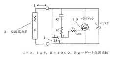
また、図8では、ゲート回路にC,R、R1,R2を図のように配して、金属接点S1のb接点の信号のチャタリング対策にもなっている。チャタリングを起こすと短時間に多数回のオン・オフを繰り返すことになる。b接点がチャタリングを起こしにくい構造や接点材料にするが、回路的にもその対策をすることが望ましい。それを防止する抵抗とコンデンサの電子回路を付加する。併せて、近年の半導体スイッチの遮断スピードが速いために再起電圧の上昇スピードが速く、その電圧波形は高い高周波成分を持つ。高周波ノイズを発生すると、直流スイッチが電流遮断するノイズによる関連電子回路の誤動作を発生する可能性がある。半導体スイッチの遮断スピードを遅くする回路を付加する。 Further, in FIG. 8, C, R, R1, and R2 are arranged in the gate circuit as shown in the figure to prevent chattering of the signal at the b contact of the metal contact S1. When chattering occurs, it is repeatedly turned on and off many times in a short time. Although the b-contact has a structure or contact material that hardly causes chattering, it is desirable to take measures against the circuit. Add an electronic circuit of resistors and capacitors to prevent it. In addition, since the recent semiconductor switch cut-off speed is fast, the reactivation voltage rises quickly, and the voltage waveform has a high-frequency component. When high-frequency noise is generated, there is a possibility that a malfunction of the related electronic circuit is generated due to noise that the DC switch interrupts current. Add a circuit to slow down the shutoff speed of the semiconductor switch.
これはドレイン−ゲート間の抵抗に並列の例えば0.01μFのコンデンサCを接続し、ゲート−ソース間に例えば100Ωの低抵抗Rで短絡すると遮断電圧の上昇はミラー積分効果で遅くなる。これはMOSFETのゲート電圧の活性領域を使った回路になるが、先のドレインーゲート間をつなぐ抵抗R1に並列に接続し、ゲートーソース間をつなぐb接点に並列に高抵抗R2、ここでは500kΩを挿入すれば、チャタリングの防止に効果が有る。CとRで再起電圧の立ち上がりスピードは、遅くできる。
特許文献2の特許願2015−199768「再起電圧制御装置」によれば、再起電圧Vrは、ドレイン‐ゲート間のコンデンサをC、ゲート‐ソース間の抵抗をRとすれば、ミラー積分理論から、Cに流れる電流で閾値電圧Vthが維持されると考えられるので、
Vr=Vth*Time/RC
である。Vth=3V, R=100Ω、C=0.01μFであれば、再起電圧は1マイクロ秒で3Vの上昇、3V/μSである。For example, when a capacitor C of 0.01 μF, for example, is connected in parallel with the resistance between the drain and the gate, and the short-circuit with a low resistance R of, for example, 100Ω is connected between the gate and the source, the increase in the cutoff voltage is delayed by the Miller integration effect. This is a circuit that uses the active region of the gate voltage of the MOSFET, but it is connected in parallel to the resistor R1 that connects the drain and gate, and the high resistance R2, in this case, 500 kΩ, in parallel to the b contact that connects the gate and source. Inserting it is effective in preventing chattering. The rising speed of the re-emergence voltage can be slowed by C and R.
According to Japanese Patent Application No. 2015-199768 “Restart Voltage Control Device” of
Vr = Vth * Time / RC
It is. If Vth = 3V, R = 100Ω, and C = 0.01 μF, the re-emergence voltage will increase 3 V in 1 microsecond and 3 V / μS.
このようにパワー用のスイッチ用MOSFETは近年目覚ましく発展しており、スイッチング損を少なくするために。高速動作を必要としてきたが、半導体スイッチの損失が許容するならば、遮断スピードを必要なだけ下げることができる。遮断スピードが遅いほど高周波ノイズは少なくなる。特に遮断器の補助のために用途を限った場合は、繰り返しサイクルが限られているので、半導体の発熱を除去するのが容易、パルス大電流が流せて、その後、ゆっくりと遮断が可能である。
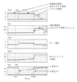
図9は直流電流開閉の過渡状態をシミュレーションするためのシミュレーション回路図を示す。図10はシミュレーションの結果の電流、電圧波形を示す。(a)は接点とMOSFETの電流波形、バリスタの電流波形である。(b)は接点極間電圧で電源電圧100Vが遮断後インダクタンスのために300Vまで上昇、最後はバリスタによってカットされている。(c)はゲート電圧、(d)はMOSFETの電圧と電流を掛けたパワーを積分した損失をジュールで表している。逆電流阻止ダイオードを入れたことでゲート電圧が1.2V、上がった結果、損失が3分の1になっている。
図11は、図10の時間軸を拡大した図である。接点間電圧では、300Vまで300μSで上昇するのが見える。As described above, the power switching MOSFET has been remarkably developed in recent years in order to reduce the switching loss. Although high speed operation has been required, if the loss of the semiconductor switch allows, the shutoff speed can be lowered as much as necessary. The higher the cutoff speed, the less high frequency noise. Especially when the application is limited to assist the circuit breaker, the repetition cycle is limited, so it is easy to remove the heat generated from the semiconductor, and a large pulse current can flow, and then it can be shut off slowly. .
FIG. 9 shows a simulation circuit diagram for simulating a transient state of DC current switching. FIG. 10 shows current and voltage waveforms as a result of the simulation. (A) is a current waveform of a contact and a MOSFET, and a current waveform of a varistor. (B) is a contact-to-contact voltage, and the power supply voltage 100V is increased to 300V due to inductance after being cut off, and finally is cut by a varistor. (C) represents the gate voltage, and (d) represents the loss, which is obtained by integrating the power multiplied by the MOSFET voltage and current, in joules. Inserting a reverse current blocking diode increases the gate voltage by 1.2V, resulting in a loss of 1/3.
FIG. 11 is an enlarged view of the time axis of FIG. It can be seen that the voltage between the contacts increases at 300 μS up to 300V.
〔第4実施形態:図12〕
図12は、本発明に係る直流電源の開閉スイッチの第4実施形態を示す回路図である。
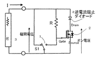
ゲートに抵抗Rを介してドレイン電圧を印加してMOSFETをオン状態にする構成では、オン電圧は閾値電圧であるVthまでしか下がらない。オン電圧をさらに下げるには、ゲートにより高い電圧を与える必要がある。そこで、金属接点のa接点とMOSFETのドレインの間に、ダイオードを順方向に入れ、ダイオード順方向電圧を加えて抵抗Rを介してゲートに電圧を与えると、ダイオードの電圧が加わった分、MOSFETのオン電圧が下がる。実験によると、MOSFETに5Aの電流が流して、ダイオードを含めた極間電圧は4.2Vに上がったがオン電圧を測ると閾値3Vより低い1Vにさがる。ドレインにダイオードの順方向電圧1.2Vも加えて、極間電圧は1.2V上がるが、無アークの条件である10V以下であるならば良いので、MOSFETのオン電圧が3Vから1Vに下がったことで、半導体の損失が3分の1になる。また、ダイオードを入れることによって、逆電流阻止にすることができる。これは負荷側に電圧が残っている負荷の場合、遮断後に電流が逆流する可能性を除くために、必要がある。一般にMOSFETのゲート電極はソースに対して+/−15V程度以上の電圧が発生しないようにダイオードでクランプしてあるので逆電圧は問題ない。また、ダイオードの順方向電圧の代わりに1Ω以下の低い抵抗を挿入して電流による抵抗ドロップ電圧でも、半導体のオン電圧を下げる効果がある。[Fourth Embodiment: FIG. 12]
FIG. 12 is a circuit diagram showing a fourth embodiment of the open / close switch of the DC power supply according to the present invention.
In the configuration in which the drain voltage is applied to the gate via the resistor R to turn on the MOSFET, the on-voltage is lowered only to the threshold voltage Vth. In order to further lower the on-voltage, it is necessary to apply a higher voltage to the gate. Therefore, when a diode is inserted in the forward direction between the a contact of the metal contact and the drain of the MOSFET, and a diode forward voltage is applied to apply a voltage to the gate through the resistor R, the amount of the diode voltage is added. The on-state voltage decreases. According to an experiment, a current of 5 A flows through the MOSFET, and the voltage between the electrodes including the diode has increased to 4.2 V. However, when the ON voltage is measured, the voltage decreases to 1 V which is lower than the threshold value 3 V. The forward voltage of the diode 1.2V is also added to the drain, and the voltage between the electrodes increases by 1.2V. However, it is sufficient if the voltage is 10V or less, which is an arc-free condition, so the MOSFET on-state voltage has decreased from 3V to 1V. As a result, the semiconductor loss is reduced to one third. Moreover, reverse current blocking can be achieved by inserting a diode. This is necessary in the case of a load in which voltage remains on the load side in order to eliminate the possibility that the current flows backward after the interruption. In general, the gate electrode of the MOSFET is clamped with a diode so that a voltage of about +/− 15 V or more is not generated with respect to the source, so that the reverse voltage is not a problem. In addition, a low resistance of 1Ω or less is inserted instead of the forward voltage of the diode, and a resistance drop voltage due to a current has an effect of reducing the on-voltage of the semiconductor.
直流電流の逆流の阻止をダイードで可能にする前の回路をさらに応用を広くしたのが、図13である。交流または直流であっても電流の方向が場合によって変化する用途がある。直流配電の直流バス間を接続する場合、電圧は一方向であるが電流は双方向である。その場合、図12の回路を電流双方向用に改良したのが図13である。 FIG. 13 shows a wider application of the circuit before enabling the reverse current of the DC current to be prevented by the diode. There are applications in which the direction of the current changes depending on the case even when the current is AC or DC. When connecting the DC buses of DC distribution, the voltage is unidirectional but the current is bidirectional. In that case, FIG. 13 shows an improvement of the circuit of FIG.
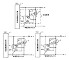
〔第5実施形態:図14及び図15〕
交流用の開閉器も多頻度開閉を行うと、アークによる電極消耗が開閉器の寿命となる。アークを最小限にするか、無アークで遮断するのが望ましい。3相交流の電流瞬断は3相同時に遮断するように、連動する1つのb接点のオン信号で三相の3つの半導体スイッチを同時にオフする。[Fifth Embodiment: FIGS. 14 and 15]
When an AC switch is also frequently opened and closed, the electrode wear due to arcing becomes the life of the switch. It is desirable to minimize arcing or cut off without arcing. The three-phase three semiconductor switches are simultaneously turned off by the ON signal of one interlocking b contact so that the three-phase alternating current instantaneous interruption is interrupted at the same time.
図14は、本発明に係る、電流が両方向の直流電力系、または交流電力系にも使用可能な開閉スイッチの第5の実施形態を示す回路図である。
図14は金属接点を連続通電する主接点S1とするとその両極にダイオードブリッジを接続し、ダイオードブリッジの直流出力プラスにMOSFETのドレインを、出力マイナスをMOSFETのソースを接続する。MOSFETのゲートは、1つ目は例えば22Ωの低抵抗Rで補助接点または連動する接点のb接点に接続する。MOSFETのゲートは、2つ目は例えば100kΩの高抵抗R1を介してMOSFETのドレインに、同じく、R1には並列にコンデンサ、例えばここでは0.1μFであるが、を並列に接続してある。MOSFETのゲートの3つ目は、例えば500kΩの高抵抗R2を介してドレインに接続してある。抵抗RとコンデンサCが連動接点Sbのb接点のオンで、半導体はオフされるがその再起電圧を緩やかに上昇させる。ダイオードブリッジを介して主接点に並列接続されているので、交流電流、方向の変化する直流にも対応できる。FIG. 14 is a circuit diagram showing a fifth embodiment of an on-off switch that can be used in a DC power system in which the current is bidirectional or an AC power system according to the present invention.
In FIG. 14, when a metal contact is a main contact S1 that is continuously energized, a diode bridge is connected to both poles thereof, the MOSFET drain is connected to the DC output plus of the diode bridge, and the output minus is connected to the source of the MOSFET. The first gate of the MOSFET is connected to the auxiliary contact or the contact b of the interlocking contact with a low resistance R of, for example, 22Ω. The second gate of the MOSFET is connected in parallel to the drain of the MOSFET through a high resistance R1 of, for example, 100 kΩ, and in parallel to R1, a capacitor, for example 0.1 μF in this case. The third gate of the MOSFET is connected to the drain via a high resistance R2 of 500 kΩ, for example. The resistor R and the capacitor C are turned on when the b contact of the interlocking contact Sb is turned on, and the semiconductor is turned off, but the re-emergence voltage is gradually increased. Since it is connected in parallel to the main contact via a diode bridge, it can also handle alternating current and direct current whose direction changes.
シリコンカーバイトで構成されるSiC−MOSFETを用いるとSiCの性質で高耐圧のスイッチが実現できる。高耐圧の使用に耐える電流スイッチが可能になるが、SiCのMOSFETのシュレフォルド電圧VthがシリコンのMOSFETより高く7V程度あって、ダイオードブリッジによる電圧降下は2Vから3Vあるので、それを加えると主接点遮断の直後に極間電圧10V以上になる。SiCのMOSFETを用いる場合は、ゲート電圧を15V程度加えて飽和状態のオンになって、シリコンのMOSFETと同じ、数V以下にならないといけない。このために絶縁したゲート電圧をゲートに別に加えて、それをb接点で短絡、またはマイナスの電圧を印加してスイッチをオフするのを推奨する。 When a SiC-MOSFET composed of silicon carbide is used, a switch having a high breakdown voltage can be realized due to the nature of SiC. Although a current switch that can withstand the use of a high withstand voltage is possible, the threshold voltage Vth of the SiC MOSFET is about 7V higher than that of the silicon MOSFET, and the voltage drop due to the diode bridge is 2V to 3V. Immediately after the contact is cut off, the interelectrode voltage becomes 10 V or more. When a SiC MOSFET is used, the gate voltage must be about 15V to turn on the saturation state, and the voltage must be several volts or less, the same as the silicon MOSFET. For this purpose, it is recommended to apply an insulated gate voltage separately to the gate and short-circuit it at the b contact or apply a negative voltage to turn off the switch.
〔第6実施形態:図15〕
三相交流用半導体スイッチとして、従来はトライアック3つで構成される簡単な半導体スイッチでは、トライアックの性質上、電流ゼロ点で遮断する。その場合、最初の1相の電流ゼロ点で遮断された後、残り2相は単相状態になって、電流ゼロになった時点で同時に遮断される。すなわち、2相を遮断しているにすぎないので負荷の中性点電位の急峻な過電圧など過渡現象が生じる。ここで目指すのは半導体スイッチによる3相同時遮断である。[Sixth Embodiment: FIG. 15]
Conventionally, as a three-phase AC semiconductor switch, a simple semiconductor switch composed of three triacs cuts off at a current zero point due to the nature of the triac. In that case, after the current is shut off at the first one-phase current zero point, the remaining two phases are in a single-phase state and are shut off simultaneously when the current becomes zero. That is, since only the two phases are cut off, a transient phenomenon such as an abrupt overvoltage of the neutral point potential of the load occurs. The aim here is to simultaneously shut off the three phases by a semiconductor switch.
図15は3相交流用に構成された本発明の実施例である。ここでは主接点のa接点と補助接点のb接点が使われている。補助接点bがオンの場合、全てのスイッチがオフされる。b接点が離れるとゲートはオンになることで、半導体スイッチが通電され、後から、主接点のa接点がオンになって、その後、電気抵抗の低い金属接点にほとんどの電流が流れる。 FIG. 15 shows an embodiment of the present invention configured for three-phase alternating current. Here, the a contact of the main contact and the b contact of the auxiliary contact are used. When the auxiliary contact b is on, all the switches are turned off. When the b contact is released, the gate is turned on so that the semiconductor switch is energized. After that, the a contact of the main contact is turned on, and then most of the current flows through the metal contact with low electrical resistance.
補助接点bが3相交流用の3接点の開閉器に1つの場合、1つの補助接点bのオンによって、3つのゲート用絶縁された電源がゲート電圧をゼロになるようにする。図15では、さらに安全スイッチが半導体スイッチ回路に直列に接続されている。この安全スイッチがオフされると半導体スイッチ部が主回路から切り離される。安全スイッチは主回路のオンの前のタイミングで接続され、遮断完了後に速やかにオフされる。安全スイッチの存在がオフ時の安全性が接点と半導体の2重になることで信頼性が増すためであって、動作のタイミングやスピードは問わない。また、この安全スイッチは常時オフ状態で主接点の投入、遮断動作の間のみ、オン状態にするようにしてもよい。 When there is one auxiliary contact b in a three-contact switch for three-phase alternating current, one of the auxiliary contacts b is turned on so that three insulated power supplies for the gates have zero gate voltage. In FIG. 15, a safety switch is further connected in series with the semiconductor switch circuit. When this safety switch is turned off, the semiconductor switch part is disconnected from the main circuit. The safety switch is connected at a timing before the main circuit is turned on, and is quickly turned off after completion of the shutoff. This is because the safety is increased when the safety switch is turned off because the safety is doubled between the contact and the semiconductor, and the timing and speed of the operation do not matter. In addition, this safety switch may be in an on state only during the turning on / off operation of the main contact in the always off state.
交流専用の無アーク低ノイズ開閉器は、MOSFETをサイリスタやトライアックに置き換えることができる。MOSFETより、高耐圧で短時間の通電耐量に優れている。また電流ゼロ点で自然消弧するので、インダクタンス電流遮断による過電圧が生じないという利点もある。しかし、容量性の負荷の場合、電流ゼロで遮断した後、再起電圧がステップ的上昇の問題もある。そのため、サイリスタ、トライアックの再起電圧上昇スピードを制限するためにコンデンサと抵抗の直列接続によるサージ・アブソーバを設置する必要がある。 An arc-free low-noise switch dedicated to AC can replace MOSFETs with thyristors and triacs. It is superior to MOSFETs in high withstand voltage and short-time withstand capability. Further, since the arc is naturally extinguished at the zero current point, there is an advantage that no overvoltage is generated due to the inductance current interruption. However, in the case of a capacitive load, there is also a problem that the regenerative voltage increases stepwise after being interrupted at zero current. For this reason, it is necessary to install a surge absorber with a capacitor and resistor connected in series to limit the speed at which the thyristor and triac re-start voltage rise.
[実施例7:図16]
図16は、請求項7の実施例で本発明に係る直流用、無アーク低ノイズ開閉器の手法をトライアックに代えて交流用の無アーク低ノイズ開閉器に応用したものである。交流の金属接点の開閉であっても、無アークで遮断出来れば接点の寿命が延び、アークが消滅時の裁断サージの発生を防止することができる。本実施例ではa接点とb接点がともにオフの遷移状態の場合、トライアックのゲートにはCとRを介してトリガーに必要な電流が供給されるように、本実施例では、Cは0.1μF、Rは100Ωを選択している。b接点がオンになるとゲート電流はゼロになるのでトライアックは電流ゼロになるとオフになる。電流ゼロ点でオフになると再起電圧が急峻に発生するが、その電圧上昇率をb接点がオンすることでCとRの直列回路がサージ・アブソーバとなって作用し、ノイズの発生を防ぐことができる。
単に抵抗だけでもトライアックをオンすることはできるが、しかし、オフ時のリーク電流を増やすのみで、サージ発生を抑える効果はないが、CとRのサージ・アブソーバを使ってゲートをオンすることで、無アークでノイズの発生を抑えた開閉が実現できる。[Example 7: FIG. 16]
FIG. 16 shows an embodiment of
Although the triac can be turned on simply by resistance, it does not have the effect of suppressing the surge by only increasing the leakage current at the off time, but by turning on the gate using the surge absorber of C and R, It can be opened and closed without arcing and with reduced noise.
1 主接点S1:金属接点
2 半導体スイッチ(MOSFET、IGBTなど絶縁ゲートのスイッチ)
3 直流電力系
4 バリスタ
5 C:コンデンサ
6 R:抵抗
7 Rg:ゲート抵抗
8 逆電流阻止ダイオード
9 ダイオードブリッジ
10 トライアック
11 安全スイッチ1 Main contact S1:
3
Claims (8)
単極双投の金属接点開閉器のコモン電極とノルマルオープンのa接点を連続通電用の主接点として、そのa接点とコモン電極には、それぞれMOSFETのドレインとソースを接続し、ゲートはノルマルクローズのb接点にゲート抵抗Rgを介して接続して、MOSFETのゲートには別途用意した絶縁された電源から電圧を与えられてMOSFETはオン状態になっているが、b接点がオンになるとゲート電圧が減少するのでMOSFETがオフになる。主接点極間の電圧はアーク発生に必要な電圧、約10V以下であるので、無アークで接点電流がMOSFETに転流し、バウンス時間後にb接点がオンになると、ゲート抵抗のミラー積分効果でソフトにオフ状態になることを特徴とする直流電流の無アーク開閉装置。A switch for opening and closing a direct current, in order to enable a break without arc,
The common electrode of the single-pole double-throw metal contact switch and the normally open a contact are the main contacts for continuous energization, and the drain and source of the MOSFET are connected to the a contact and the common electrode, respectively, and the gate is normally closed. The gate of the MOSFET is connected via a gate resistor Rg, and a voltage is applied to the gate of the MOSFET from a separately prepared isolated power supply. The MOSFET is turned on, but when the b contact is turned on, the gate voltage Decreases, the MOSFET is turned off. Since the voltage between the main contact electrodes is less than about 10V, which is necessary for arc generation, the contact current is commutated to the MOSFET without arcing, and when the b contact is turned on after the bounce time, the gate resistance is softened by the Miller integral effect. A direct-current arc-free switchgear characterized by being turned off.
Priority Applications (1)
| Application Number | Priority Date | Filing Date | Title |
|---|---|---|---|
| JP2016013814A JP6713660B2 (en) | 2016-01-11 | 2016-01-11 | Arc-free current switchgear |
Applications Claiming Priority (1)
| Application Number | Priority Date | Filing Date | Title |
|---|---|---|---|
| JP2016013814A JP6713660B2 (en) | 2016-01-11 | 2016-01-11 | Arc-free current switchgear |
Publications (2)
| Publication Number | Publication Date |
|---|---|
| JP2017126544A true JP2017126544A (en) | 2017-07-20 |
| JP6713660B2 JP6713660B2 (en) | 2020-06-24 |
Family
ID=59364314
Family Applications (1)
| Application Number | Title | Priority Date | Filing Date |
|---|---|---|---|
| JP2016013814A Active JP6713660B2 (en) | 2016-01-11 | 2016-01-11 | Arc-free current switchgear |
Country Status (1)
| Country | Link |
|---|---|
| JP (1) | JP6713660B2 (en) |
Cited By (4)
| Publication number | Priority date | Publication date | Assignee | Title |
|---|---|---|---|---|
| CN110690078A (en) * | 2019-09-30 | 2020-01-14 | 国源容开国际科技(北京)股份有限公司 | Diode equal zero phase switch with fault protection |
| JP7250266B1 (en) | 2022-07-19 | 2023-04-03 | 隆一 嶋田 | DC current interrupter |
| CN116260436A (en) * | 2022-12-30 | 2023-06-13 | 合肥仙湖半导体科技有限公司 | Arc-discharge-free insulated three-phase switch and application circuit thereof |
| JP7417293B2 (en) | 2019-03-29 | 2024-01-18 | ナノブリッジ・セミコンダクター株式会社 | Logic integrated circuit and control method using logic integrated circuit |
Families Citing this family (1)
| Publication number | Priority date | Publication date | Assignee | Title |
|---|---|---|---|---|
| JP7165317B1 (en) | 2022-06-13 | 2022-11-04 | 隆一 嶋田 | DC switchgear |
Citations (6)
| Publication number | Priority date | Publication date | Assignee | Title |
|---|---|---|---|---|
| JPS61138125U (en) * | 1985-02-18 | 1986-08-27 | ||
| JPH04354374A (en) * | 1991-05-31 | 1992-12-08 | Fuji Electric Co Ltd | Hybrid switch |
| US5652688A (en) * | 1995-09-12 | 1997-07-29 | Schweitzer Engineering Laboratories, Inc. | Hybrid circuit using miller effect for protection of electrical contacts from arcing |
| JP2000036238A (en) * | 1998-04-06 | 2000-02-02 | Shigeisa Imoto | Switch circuit |
| JP2009267742A (en) * | 2008-04-24 | 2009-11-12 | Panasonic Electric Works Co Ltd | Operation terminal |
| JP2014216056A (en) * | 2013-04-22 | 2014-11-17 | 富士電機株式会社 | Dc circuit breaker device |
-
2016
- 2016-01-11 JP JP2016013814A patent/JP6713660B2/en active Active
Patent Citations (6)
| Publication number | Priority date | Publication date | Assignee | Title |
|---|---|---|---|---|
| JPS61138125U (en) * | 1985-02-18 | 1986-08-27 | ||
| JPH04354374A (en) * | 1991-05-31 | 1992-12-08 | Fuji Electric Co Ltd | Hybrid switch |
| US5652688A (en) * | 1995-09-12 | 1997-07-29 | Schweitzer Engineering Laboratories, Inc. | Hybrid circuit using miller effect for protection of electrical contacts from arcing |
| JP2000036238A (en) * | 1998-04-06 | 2000-02-02 | Shigeisa Imoto | Switch circuit |
| JP2009267742A (en) * | 2008-04-24 | 2009-11-12 | Panasonic Electric Works Co Ltd | Operation terminal |
| JP2014216056A (en) * | 2013-04-22 | 2014-11-17 | 富士電機株式会社 | Dc circuit breaker device |
Cited By (5)
| Publication number | Priority date | Publication date | Assignee | Title |
|---|---|---|---|---|
| JP7417293B2 (en) | 2019-03-29 | 2024-01-18 | ナノブリッジ・セミコンダクター株式会社 | Logic integrated circuit and control method using logic integrated circuit |
| CN110690078A (en) * | 2019-09-30 | 2020-01-14 | 国源容开国际科技(北京)股份有限公司 | Diode equal zero phase switch with fault protection |
| JP7250266B1 (en) | 2022-07-19 | 2023-04-03 | 隆一 嶋田 | DC current interrupter |
| JP2024012743A (en) * | 2022-07-19 | 2024-01-31 | 隆一 嶋田 | Dc component correction part |
| CN116260436A (en) * | 2022-12-30 | 2023-06-13 | 合肥仙湖半导体科技有限公司 | Arc-discharge-free insulated three-phase switch and application circuit thereof |
Also Published As
| Publication number | Publication date |
|---|---|
| JP6713660B2 (en) | 2020-06-24 |
Similar Documents
| Publication | Publication Date | Title |
|---|---|---|
| Shukla et al. | A survey on hybrid circuit-breaker topologies | |
| US7079363B2 (en) | Hybrid DC electromagnetic contactor | |
| KR101521545B1 (en) | Device and method to interrupt high voltage direct current | |
| EP3093941B1 (en) | Direct current circuit breaker and method using the same | |
| JP6713660B2 (en) | Arc-free current switchgear | |
| EP3651175B1 (en) | Circuit-breaker with reduced breakdown voltage requirement | |
| CN106663557B (en) | For interrupting the separating switch of DC current | |
| Peng et al. | Current commutation in a medium voltage hybrid DC circuit breaker using 15 kV vacuum switch and SiC devices | |
| CN108141209B (en) | Circuit for isolating load from source | |
| CN104779593A (en) | Direct-current solid circuit breaker and control method thereof | |
| KR102298006B1 (en) | Method and voltage multiplier for converting input voltage, and blocking circuit | |
| CN109950866B (en) | Current breaker | |
| JP2017191764A (en) | Silence arc current connection device | |
| CN102064047A (en) | Relay and switching tube parallel circuit suitable for high-pressure direct current occasion | |
| JP2018125270A (en) | DC power system safety switchgear | |
| CN109861189B (en) | Arc extinguishing type low-voltage direct current breaker | |
| WO2017016501A1 (en) | Inrush-current free switching device and control method thereof | |
| JP2021034124A (en) | DC current switchgear | |
| JP6646902B2 (en) | Electromotive force control device | |
| CN115065039A (en) | Hybrid circuit breaker | |
| JP2018032611A (en) | Ac current switchgear | |
| JP6694177B2 (en) | DC breaker | |
| JP7017758B2 (en) | DC current switchgear using reed relay | |
| JP7250266B1 (en) | DC current interrupter | |
| Tang et al. | Multi-stage DC hybrid switch with slow switching |
Legal Events
| Date | Code | Title | Description |
|---|---|---|---|
| RD02 | Notification of acceptance of power of attorney |
Free format text: JAPANESE INTERMEDIATE CODE: A7422 Effective date: 20181114 |
|
| A621 | Written request for application examination |
Free format text: JAPANESE INTERMEDIATE CODE: A621 Effective date: 20181115 |
|
| A521 | Request for written amendment filed |
Free format text: JAPANESE INTERMEDIATE CODE: A821 Effective date: 20181115 |
|
| A977 | Report on retrieval |
Free format text: JAPANESE INTERMEDIATE CODE: A971007 Effective date: 20190808 |
|
| A131 | Notification of reasons for refusal |
Free format text: JAPANESE INTERMEDIATE CODE: A131 Effective date: 20190925 |
|
| A601 | Written request for extension of time |
Free format text: JAPANESE INTERMEDIATE CODE: A601 Effective date: 20191120 |
|
| A521 | Request for written amendment filed |
Free format text: JAPANESE INTERMEDIATE CODE: A523 Effective date: 20200114 |
|
| TRDD | Decision of grant or rejection written | ||
| A01 | Written decision to grant a patent or to grant a registration (utility model) |
Free format text: JAPANESE INTERMEDIATE CODE: A01 Effective date: 20200518 |
|
| A61 | First payment of annual fees (during grant procedure) |
Free format text: JAPANESE INTERMEDIATE CODE: A61 Effective date: 20200521 |
|
| R150 | Certificate of patent or registration of utility model |
Ref document number: 6713660 Country of ref document: JP Free format text: JAPANESE INTERMEDIATE CODE: R150 |
|
| R250 | Receipt of annual fees |
Free format text: JAPANESE INTERMEDIATE CODE: R250 |