JP2017191764A - Silence arc current connection device - Google Patents
Silence arc current connection device Download PDFInfo
- Publication number
- JP2017191764A JP2017191764A JP2016094132A JP2016094132A JP2017191764A JP 2017191764 A JP2017191764 A JP 2017191764A JP 2016094132 A JP2016094132 A JP 2016094132A JP 2016094132 A JP2016094132 A JP 2016094132A JP 2017191764 A JP2017191764 A JP 2017191764A
- Authority
- JP
- Japan
- Prior art keywords
- contact
- current
- semiconductor switch
- arc
- gate
- Prior art date
- Legal status (The legal status is an assumption and is not a legal conclusion. Google has not performed a legal analysis and makes no representation as to the accuracy of the status listed.)
- Granted
Links
Images


Abstract
Description
本発明は直流電力系で用いる開閉器、プラグ、コンセントなど接続装置に関する。 The present invention relates to a connection device such as a switch, a plug, and an outlet used in a DC power system.
本発明は、直流電流の開閉器、プラグとコンセントなど接続装置に関し、直流電力系統、太陽光発電、電気鉄道、電気自動車、屋内配線等において必要な電流の開閉、接続装置に属し、直流電流を通電中において遮断するにアークを発生すること無く遮断可能になるように、半導体スイッチと、導通損失の低い金属接点スイッチとで構成される直流接続装置に関する。 The present invention relates to a connecting device such as a DC current switch, plug and outlet, and belongs to a connecting / switching device required for a DC power system, solar power generation, electric railway, electric vehicle, indoor wiring, etc. The present invention relates to a direct current connection device composed of a semiconductor switch and a metal contact switch with low conduction loss so that it can be interrupted without generating an arc when it is energized.
近年、半導体スイッチの進歩により、絶縁ゲートを持ったパワーMOSFETやIGBTなどで高電圧・大電流が高速に遮断可能になったが、半導体デバイスはまだ、金属接点に較べれば、通電中の電気抵抗が大きく、発熱が生じ、何らかの冷却機構が必要である。一方、直流電流の遮断を金属接点の開極で行うと電流が遮断されずにアーク放電となって電流が連続する。開極時に発生する高温のアークにより接点金属を溶かし消耗し、アークを消滅させなければ電流は遮断できない。アークを消弧するにはアーク長を磁気などで長くし、消弧するが、電極が消耗して接点の寿命が短くなってしまう。さらに直流の接続装置(コネクター)、プラグ・コンセントも通電中に接続を停止・断線状態にすることができない問題があった。 In recent years, with the advancement of semiconductor switches, high voltage and large current can be cut off at high speed with power MOSFETs and IGBTs with insulated gates, but semiconductor devices are still more resistant to electrical resistance than metal contacts. Is large, heat is generated, and some kind of cooling mechanism is required. On the other hand, when the direct current is interrupted by opening the metal contact, the current is not interrupted and arc discharge occurs and the current continues. The contact metal is melted and consumed by the high-temperature arc generated during the opening, and the current cannot be interrupted unless the arc is extinguished. In order to extinguish the arc, the arc length is increased by magnetism or the like to extinguish the arc, but the electrode is consumed and the life of the contact is shortened. Furthermore, there has been a problem that the DC connection device (connector), plug, and outlet cannot be stopped or disconnected while power is being supplied.
近年シリコン・カーバイド系の半導体が実用化されて、MOSFET(Metal Oxide Semiconductor Field Effect Transistor)で数kVの高耐電圧の半導体スイッチが実用化されようとしている。この高耐圧の半導体スイッチを使って、これまで金属接点では困難であった高電圧の直流電力系の開閉、遮断スイッチが提供できるようになった。しかし、まだまだ、半導体スイッチの通電損は金属接点より大きく、連続通電では半導体スイッチの冷却装置が必要となり、大型になってしまうのが欠点である。そこで、両方の利点を組み合わせて、通電は金属接点で、遮断時のみ半導体スイッチで通電、遮断する無アーク開閉器、遮断器が望まれている。 In recent years, silicon carbide semiconductors have been put into practical use, and high-withstand-voltage semiconductor switches of several kV are being put into practical use in MOSFETs (Metal Oxide Field Effect Effect Transistors). Using this high withstand voltage semiconductor switch, it has become possible to provide an open / close switch for a high voltage DC power system, which has been difficult with metal contacts. However, the energization loss of the semiconductor switch is still larger than that of the metal contact, and the continuous energization requires a cooling device for the semiconductor switch, resulting in a large size. Therefore, by combining both advantages, there is a demand for an arc-free switch and a circuit breaker that are energized by a metal contact and energized and interrupted by a semiconductor switch only at the time of interruption.
本発明は特許5864006に記載した金属接点と半導体スイッチの並列接続による無アーク開閉器の欠点を除き、さらに効果を増し、応用範囲を広げる改良に関するものである。また、先行特許文献2では、「電力用途でスイッチを構成する場合、金属接点のみで完全に遮断する回路が必要とされる場合がある。」と記されて「IGBTに直列に機械スイッチを入れる必要があることを意味する」とある。本発明にもそのスイッチを追加する必要がある。それがS1であって、導通する時は最初にS1がオンされ、遮断時は、S1は最後にオフされる。 The present invention relates to an improvement in which the effect is further increased and the application range is expanded, except for the disadvantages of the arc-free switch formed by parallel connection of metal contacts and semiconductor switches described in Japanese Patent No. 5864006. Further, in the
ところで、先記特許文献1の図7に示された直流電流の遮断支援回路は、常時、半導体スイッチが接続されており、開極時、並列の半導体回路の常時並列に接続されていることの信頼性が問題になるうえに、ゲート回路を通じてわずかな電流のリークがあることも欠点であった。また、金属接点のa接点は主回路電流が流れるが、遅れてb接点がオンする時間遅れを利用して、半導体スイッチをオフするタイミングに使うが、b接点はa接点のように大電流を扱わず、絶縁ゲートの電位を短絡するのみで数Vで数mAの弱電流である。接点には不完全な接触問題、チャタリング問題の少ない弱電流用のスイッチを用いるほうが合理的である。
半導体に流れる時間が先行特許文献1に記載の双投スイッチでは電極aからbまでの反転時間であって、それは数mSで、かなり短く半導体の通電容量では十分効果のあることであるが、短時間の半導体の電流容量は十分にあるので数10mSと短時間でなくてもよく、通電接点とゲート制御のスイッチS2はスイッチS1とS3の間のタイミングで作動し、連動していればよいのである。By the way, in the DC current interruption support circuit shown in FIG. 7 of the above-mentioned
In the double throw switch described in the
本発明は上記の点に鑑みなされたものであり、その目的はゲート駆動電源、タイマーなど不要で、簡易な回路構成で、導通している電流を遮断する際に、半導体スイッチでバイパスして、金属接点のアークを発生させずに、短時間のみ半導体スイッチに転流させて後、半導体スイッチで電流を遮断する機能を備え、導通時はバイパスする機械接点S3があって、さらにリーク電流を防ぐために電流遮断後に完全に極間を断路する機械接点S1で構成する開閉器、プラグ・コネクタなど接続装置を提供することにある。 The present invention has been made in view of the above points, and its purpose is not to require a gate drive power supply, a timer, etc., and with a simple circuit configuration, when interrupting a conducting current, it is bypassed with a semiconductor switch, It has a function to cut off the current by the semiconductor switch after being commutated to the semiconductor switch for a short time without generating the arc of the metal contact, and there is a mechanical contact S3 that bypasses when conducting, further preventing leakage current. Therefore, it is an object of the present invention to provide a connection device such as a switch, a plug, or a connector constituted by a mechanical contact S1 that completely disconnects the electrodes after the current is interrupted.
上記目的を達成するために、本発明によれば、直流電源に負荷を接続・開放する手順を図1にて説明する。
接続するには
(1)最初にS1がオンすると半導体回路を接続するが、半導体スイッチはゲートがS2 b接点に接続されており、ゲート制御の電圧がゼロで半導体スイッチはオフ状態の ままである。
(2)S2の接点が作動開始すると、b接点から外れて半導体スイッチの抵抗R1により ゲート電圧は上昇し、半導体スイッチMOSFETはセルフバイアス電圧Vth( シュレスホルド電圧)で導通する。半導体デバイスが導通状態となり負荷へと電流 が流れる。
(3)最後にS3をオンする。オン抵抗の小さな金属接点であるS3で電源と負荷間を短 絡させることで電流は主としてS3を流れるようになって、半導体にはわずかに流 れても発熱もわずかでスイッチの接続動作は完了する。In order to achieve the above object, according to the present invention, a procedure for connecting and releasing a load to a DC power supply will be described with reference to FIG.
To connect (1) When S1 is first turned on, the semiconductor circuit is connected. However, the gate of the semiconductor switch is connected to the S2b contact, the gate control voltage is zero, and the semiconductor switch remains off. .
(2) When the contact of S2 starts to operate, the gate voltage is increased by the resistance R1 of the semiconductor switch, and the semiconductor switch MOSFET becomes conductive at the self-bias voltage Vth (shreshhold voltage). The semiconductor device becomes conductive and current flows to the load.
(3) Finally, S3 is turned on. By short-circuiting between the power supply and the load at S3, which is a metal contact with low on-resistance, the current flows mainly through S3. Even if it flows slightly in the semiconductor, it generates little heat and the switch connection is completed. To do.
解放するには、
(4)最初にS3の接続装置が解放するがS2b接点がオンするまで、半導体はセルフゲ ートトリガーで導通状態であるので、全電流が半導体に流れて接点の極間はアーク が発生するに必要な約10V以上にならず、S3は無アークで開極される。
(5)つぎにS2b接点がオンするとゲート制御電圧がゼロになって半導体スイッチはオ フになって負荷への電流が遮断される。このときインダクティブな負荷を切るとサ ージ電圧が発生するので過電圧保護が必要である。
(6)微小なリーク電流の除去のため、また感電事故防止ため、機械金属接点によるS1 が、電流が微小なため無アークで閧放され、完全な開放動作が完了する。
S1,S2,S3の3つの接点の一連の動作によって開閉器の開閉、プラグ・コネクタなどの接続・開放すれば、アークの無い接続解放遮断が可能である。To release
(4) First, the connection device of S3 is released, but until the S2b contact is turned on, the semiconductor is in a conductive state by a self-gate trigger. Therefore, all current flows through the semiconductor and an arc is generated between the contacts. The voltage does not exceed about 10 V, and S3 is opened without arc.
(5) Next, when the S2b contact is turned on, the gate control voltage becomes zero, the semiconductor switch is turned off, and the current to the load is cut off. At this time, if an inductive load is cut off, a surge voltage is generated, so overvoltage protection is necessary.
(6) In order to remove a minute leakage current and to prevent an electric shock accident, S1 due to the mechanical metal contact is released without arc because the current is minute, and the complete opening operation is completed.
By opening and closing the switch and connecting / disconnecting the plug / connector through a series of operations of the three contacts S1, S2, and S3, it is possible to disconnect and release the connection without arc.
上記手順により、アーク無しで金属接点を導通、遮断解放することができる。
すなわち、S1接点の操作、その後S2接点の操作によって通電が行われ、その後、接点S3がこの電流を短絡して半導体デバイス電流はS3の導通接点に転流させる、3ステップで大電流直流を無アークで接続する、解放はこの逆である。According to the above procedure, the metal contact can be conducted, disconnected and released without an arc.
That is, energization is performed by the operation of the S1 contact, and then the operation of the S2 contact, and then the contact S3 shorts this current and the semiconductor device current is commutated to the conducting contact of S3. Arcing, release is the opposite.
これにより、交流接点では完全開放状態、すなわち空気の層で絶縁されてオフされていた開閉器、コンセント、プラグなどが、直流電流であっても、これまでに準じた安全基準で完全な開放状態であると考えられる。解放動作では、電源から接続装置を経て負荷側に流れていた電流が、前記通電接点S3が開極すると半導体スイッチがオン状態のため接点S1へ転流し、S2のb接点のオンで、直流アーク無しに半導体スイッチで遮断するがそれは接点S3が十分な開極距離を得てから行うことができる。半導体スイッチで遮断後、抵抗R1によるリーク電流を、接点S1が開極して遮断するが1mA以下の電流であるのでアークは発生しない。結局、アークを全く発生せずに直流電流を遮断する。(請求項1)S2接点はa接点であっても半導体ゲート電圧を制御できれば可能であるが。このa接点は主回路の電圧に耐える必要がある、またS1接点の接触不良で半導体ゲートに高電圧がかかる可能性があるので何らかの保護回路が必要である。S2のb接点を使って半導体を制御すればここに高電圧は発生しないので弱電流用のスイッチが使える利点がある。(請求項1) As a result, AC contacts are fully open, that is, switches, outlets, plugs, etc. that have been insulated and turned off by an air layer are fully open according to the safety standards that have been used so far, even if they are direct current. It is thought that. In the release operation, the current flowing from the power source through the connecting device to the load side is commutated to the contact S1 because the semiconductor switch is turned on when the energizing contact S3 is opened, and the DC arc is turned on when the b contact of S2 is turned on. However, this can be done after the contact S3 has a sufficient opening distance. After being cut off by the semiconductor switch, the leakage current caused by the resistor R1 is cut off by opening the contact S1, but no arc is generated because the current is 1 mA or less. Eventually, the direct current is interrupted without generating any arc. (Claim 1) Even if the S2 contact is an a contact, it is possible if the semiconductor gate voltage can be controlled. The contact a needs to withstand the voltage of the main circuit, and since a high voltage may be applied to the semiconductor gate due to poor contact of the S1 contact, some kind of protection circuit is necessary. If the semiconductor is controlled using the b contact of S2, a high voltage is not generated here, so there is an advantage that a switch for weak current can be used. (Claim 1)
このため電極の開極動作が、時間がかかっても、さらに手動であっても遮断可能になるので、直流の接続装置、プラグやコンセントなどにも無アークの信頼性の高い開閉装置、プラグ・コンセントなどを提供できる。(請求項2,3,4) For this reason, the electrode opening operation can be interrupted even if it takes time or even manually. Therefore, it is possible to connect the DC connection devices, plugs and outlets, etc. Can provide outlets. (
大電流になると半導体デバイスの通電時間が問題になる場合は、先行特許文献1の無アークの双投スイッチを反転時間が2,3mSをS2に採用すれば通電時間を最小の数msにすることができる。 If the energization time of the semiconductor device becomes a problem when a large current is applied, the energization time can be reduced to a minimum of several ms if the inversion time of 2,3 mS is adopted for S2 of the arc-free double throw switch of the
ここでS1を直流遮断能力のある機械接点、例えば磁界による吹き消し効果による直流遮断器にすれば、半導体スイッチとの直列遮断で種々の相乗効果を期待できる。ひとつは機械接点の信頼性を必要とする場合、S1を安全スイッチとして考えてもよいし、半導体スイッチが故障した場合のバックアップとして考えることもできる。金属接点による直流電流遮断はアークによる電極消耗が問題で接点の耐久性が交流に較べ大幅に低いが半導体スイッチとの直列接続でその問題を解決できる。すなわち、開閉回数が多い、負荷電流の開閉には、半導体スイッチを用い、電流が大きいが頻度の少ない事故電流の場合には、S2は動作させずに、機械接点S1で遮断するなどである。(請求項5) Here, if S1 is a mechanical contact having a DC blocking capability, for example, a DC circuit breaker with a blow-off effect by a magnetic field, various synergistic effects can be expected by series blocking with a semiconductor switch. One is that when the reliability of the mechanical contact is required, S1 may be considered as a safety switch, or as a backup when the semiconductor switch fails. Although the DC current interruption by the metal contact is a problem of electrode consumption due to the arc and the durability of the contact is significantly lower than that of the AC, the problem can be solved by series connection with the semiconductor switch. That is, a semiconductor switch is used to open and close the load current with a large number of switching times, and in the case of an accident current with a large current but a low frequency, S2 is not operated and is shut off at the mechanical contact S1. (Claim 5)
さらに直流でも電流の方向に因らず、無アークでの遮断可能な方法(請求項6,7)は、高電圧大電流の交流電流に、適用可能である。交流電流は電流ゼロ点があるので遮断が可能ではあるが、アークが発生すると電極消耗やノイズの問題が起こる。本発明の無アーク開閉を用いれば、多頻度の開閉に耐え、また遮断時にアークが起因するノイズが発生しないなどの利点がある。 Further, the method capable of interrupting without arc regardless of the direction of current even in direct current (
以下、本発明の実施の形態を図1〜図3に示す実施例1、および図4〜図9に示す実施例に基づいて説明する。 Hereinafter, embodiments of the present invention will be described based on Example 1 shown in FIGS. 1 to 3 and Examples shown in FIGS.
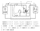
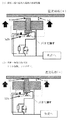
まず、本発明の実施例1による直流電源プラグ・コンセントの回路構成を図1に示す。スイッチが3つあって、 接続時のシーケンスは、S1オン→S2オン(b接点オフ)→S3オン。解放時のシーケンスは、S3オフ→S2オフ(b接点オン)→S1オフ、 である。 First, FIG. 1 shows a circuit configuration of a DC power plug / outlet according to a first embodiment of the present invention. There are three switches and the connection sequence is S1 on → S2 on (b contact off) → S3 on. The sequence at the time of release is S3 off → S2 off (b contact on) → S1 off.
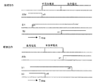
図2はスイッチと電流の関係を示した図である。図2に接続動作時のシーケンスと電流の概略を示す。接続時、電極の挿入によってS1がオンになっても、半導体スイッチがオフであるのでは電流は流れない。S1の接点がオンにしたあと、さらに挿入、S2のb接点が圧力により、b接点が開極して、ゲート電圧はVth(シュレスホルド電圧)になって、半導体スイッチはオン状態になる。最後に直流電源に接続したS3がオンして、半導体電流は抵抗の小さなS3にほとんどの電流が流れる。プラグがS1をオンし、続いてS2bをオフにして、最後にS3をオンする。 FIG. 2 is a diagram showing the relationship between the switch and the current. FIG. 2 shows an outline of the sequence and current during the connection operation. At the time of connection, even if S1 is turned on by inserting an electrode, no current flows if the semiconductor switch is off. After the contact of S1 is turned on, the contact is further inserted, the contact b of S2 is opened by pressure, the contact b is opened, the gate voltage becomes Vth (Shreshold voltage), and the semiconductor switch is turned on. Finally, S3 connected to the DC power supply is turned on, and most of the semiconductor current flows through S3 having a small resistance. The plug turns on S1, then turns off S2b, and finally turns on S3.
図2に解放動作時のシーケンスと電流の概略を示す。接続状態ではS1、S3がオン状態、S2はb接点がオフ状態で、負荷電流は主にS3で流れている。解放のためにプラグを引き抜くとまずS3が開極するがS1、半導体スイッチがON状態のため無アークで開極する。続いて、プラグを引き抜き、フリーになったS2bがb接点オンするとゲート電圧がゼロになって半導体スイッチがオフされ、負荷電流が無アークで遮断される。最後にS1の開極により残ったR1に流れる1mA以下の電流を遮断して完全な解放がなされる。 FIG. 2 shows an outline of the sequence and current during the release operation. In the connected state, S1 and S3 are in the ON state, S2 is in the OFF state, and the load current flows mainly in S3. When the plug is pulled out for release, S3 is opened first, but S1 is opened without arc because the semiconductor switch is ON. Subsequently, when the plug is pulled out and S2b, which has become free, turns on the b contact, the gate voltage becomes zero, the semiconductor switch is turned off, and the load current is interrupted without arcing. Finally, the current of 1 mA or less flowing through R1 remaining due to the opening of S1 is interrupted to completely release the current.
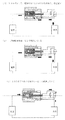
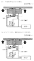
図3は図1の回路構成の1実施例である同軸状のDCプラグの構成図とプラグの抜き差しによる、スイッチS1,S2,S3を同軸状のプラグと受け側のコンセントにした動作説明図を示す。図3のプラグは電源と負荷を接続するプラグとジャックになっており、電流のリターンは別に接続してある。(請求項2)
(1)は接続前の状態
(2)プラグの挿入が開始してDCプラグS1が導通した、しかし、ゲート電圧が短絡されているので電流が流れない。
(3)挿入が進むとS2bがオフになって、MOSFETが導通状態になる。
(4)さらにプラグが挿入されて、S3がオンして導通が完了。
(5)遮断の開始。S3で導通している。
(6)S3がオフされても、その電流はMOSFETで導通されているので無アークで転流する。
(7)S2bがオンされるとゲート電圧がゼロになってMOSFETにより電流が遮断。
(8)S1も離れて完全な遮断動作が終了。
(9)プラグの解放が完了。FIG. 3 is a configuration diagram of a coaxial DC plug which is one embodiment of the circuit configuration of FIG. 1 and an operation explanatory diagram in which the switches S1, S2 and S3 are made into a coaxial plug and a receptacle on the receiving side by plugging / unplugging. Show. The plug in FIG. 3 is a plug and a jack for connecting the power source and the load, and the current return is connected separately. (Claim 2)
(1) State before connection (2) Insertion of the plug starts and the DC plug S1 becomes conductive, but no current flows because the gate voltage is short-circuited.
(3) When the insertion proceeds, S2b is turned off and the MOSFET becomes conductive.
(4) Further plugs are inserted and S3 is turned on to complete conduction.
(5) Start of blocking. Conducted at S3.
(6) Even if S3 is turned off, since the current is conducted by the MOSFET, it commutates without arc.
(7) When S2b is turned on, the gate voltage becomes zero and the current is cut off by the MOSFET.
(8) S1 also leaves and completes the shut-off operation.
(9) The plug release is complete.
図10には実施例1の回路をもちいて図3において説明したDCプラグを数Aの直流電流を無アーク遮断したことを実証している。そのDCプラグとジャック外観と極間の再起電圧の波形を示す。再起電圧は最大180V程度で,この波形からアークが発生しなかったことがわかる。アークが発生すると図のように電圧波形にプラズマ動揺による不規則な電圧が見られるからである。 FIG. 10 demonstrates that the DC plug described in FIG. The waveform of the DC plug and jack appearance and the re-emergence voltage between the electrodes is shown. The re-emergence voltage is about 180 V at maximum, and it can be seen from this waveform that no arc has occurred. This is because when an arc is generated, an irregular voltage due to plasma fluctuation is seen in the voltage waveform as shown in the figure.
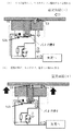
図4は本発明の実施例3の直流大電流接続装置の構造図である。(請求項3)
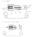
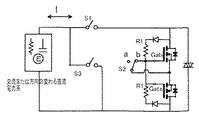
実施例3では、S1は直流母線と接触する可動接触子の中心導体である。S3は直流母線と広い面積で接触する可動接触子の外側導通導体である。中心導体は常に下からばねによって押されて導通導体より突出しており、最初にS1が母線に接触するようになっている。中心導体が母線に接触して押されるとその動作でS2がオフされるように配置されている。中心導体はMOSFETのドレインに、外部導通導体は負荷に直接つながっている。S2bはMOSFETのゲートとソースにそれぞれ接続されてノルマルクローズの接点になっている。この構造によって、S1からオンし、次にS2がオフし、最後にS3が接触して母線との接続が完了し、解放はその逆がなされる。FIG. 4 is a structural diagram of a DC large current connection device according to
In Example 3, S1 is the central conductor of the movable contact that contacts the DC bus. S3 is an outer conductive conductor of the movable contact that contacts the DC bus in a wide area. The center conductor is always pushed from below by a spring and protrudes from the conductive conductor, so that S1 first contacts the bus. It is arranged so that S2 is turned off by the operation when the central conductor is pressed in contact with the bus bar. The central conductor is directly connected to the drain of the MOSFET, and the external conductive conductor is directly connected to the load. S2b is connected to the gate and the source of the MOSFET to be a normally closed contact. With this structure, S1 is turned on, then S2 is turned off, and finally S3 comes into contact to complete the connection with the bus, and the release is reversed.
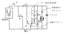
図5に再起電圧の上昇率を制御してノイズを低減するためのミラー積分効果を用いるC−R2回路を追加した。さらにMOSFETのボディーダイオードによる逆電流導通を阻止するためのダイオードをMOSFETのドレインに挿入した応用例を示す。さらにゲート逆電圧の保護のために保護ダイオードをソースーゲート間に追加している。これが15V程度の定電圧ダイオードであるとさらに順電圧の保護にも効果がある。また、S2が双投スイッチやマイクロスイッチである場合、S2のa接点があるので、それをS1に直列に用いると半導体デバイスの通電時間が双投スイッチの反転時間のみになるので、半導体の通電容量が上がる効果がある。 In FIG. 5, a C-R2 circuit using a Miller integration effect for reducing the noise by controlling the rate of increase of the regenerative voltage is added. Furthermore, an application example is shown in which a diode for preventing reverse current conduction by the body diode of the MOSFET is inserted in the drain of the MOSFET. Furthermore, a protection diode is added between the source and gate to protect the gate reverse voltage. If this is a constant voltage diode of about 15 V, it is further effective for protecting forward voltage. Further, when S2 is a double throw switch or a micro switch, since there is an a contact of S2, if it is used in series with S1, the energization time of the semiconductor device becomes only the inversion time of the double throw switch, so that the energization of the semiconductor There is an effect of increasing the capacity.
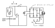
図6は実施例1の回路構成を直流電流双方向にも、さらに交流電流にも適用可能な回路構成を示す。S1とS3の間にダイオード・ブリッジを介して接続して直流化してMOSFETが半導体スイッチとして使用されて電流双方向になる。ゲートにはミラー積分効果のC−R、保護ダイオードが付いている。S2はこの場合、S1、S2回路から絶縁する必要がある。このS2b接点は弱電圧のスイッチで可能である。FIG. 6 shows a circuit configuration in which the circuit configuration of the first embodiment can be applied to both direct current and alternating current. A diode bridge is connected between S1 and S3 to make a direct current, and the MOSFET is used as a semiconductor switch to make current bidirectional. The gate is equipped with a Miller integral effect CR and a protection diode. In this case, S2 needs to be insulated from the S1 and S2 circuits. This S2b contact can be a weak voltage switch.
図7は図6の交流、または電流方向の変わる直流用の変形である。MOSFETを逆直列で電流双方向のスイッチになる。図6よりも部品数が少ない。 FIG. 7 shows a modification for the alternating current of FIG. 6 or the direct current whose current direction changes. The MOSFET becomes a current bidirectional switch in reverse series. There are fewer parts than FIG.
図8は直流プラグとコンセントの実施例である。S1、S3は金属接点が差し込みに従って順次接触する。S2bは差し込まれた中間位置に置かれており、S1がオンすると次に、b接点がオフになる、b接点がオフで半導体デバイスがオン状態になって電流が流れ、その後にS3がオンして、半導体回路をバイパスする。遮断はこの逆にS3オフ、S2bオンで電流が半導体デバイスで遮断、最後にS1が離れて開極が完了する。この回路図は最も簡単な構成の直流電流の1方向専用であるが、半導体回路を図5にして、再起電圧の制御を行うも可能、さらに図6、または図7を用いれば交流にも適用可能である。 FIG. 8 shows an embodiment of a DC plug and an outlet. In S1 and S3, the metal contacts are sequentially contacted according to the insertion. S2b is placed at the inserted intermediate position. When S1 is turned on, the b contact is turned off, the b contact is turned off, the semiconductor device is turned on, and a current flows, and then S3 is turned on. Bypassing the semiconductor circuit. On the contrary, when S3 is turned off and S2b is turned on, the current is cut off by the semiconductor device, and finally S1 is released to complete the opening. This circuit diagram is dedicated to one direction of direct current with the simplest configuration, but it is also possible to control the regenerative voltage by making the semiconductor circuit as shown in FIG. 5, and it can also be applied to alternating current using FIG. 6 or FIG. Is possible.
(その他の実施形態)
(1)上記の実施形態では半導体デバイスとしてMOSFETを使用するようとしたが、 IGBT(絶縁ゲートバイポーラトランジスタ)など絶縁ゲートをもつ電圧制御デ バイスでもよい。
(2)上記の実施形態では、接続装置に適用した場合について説明したがS1,S2,S 3が順にオン、オフすれば良いので、3スイッチ連動の手動の回転スイッチ、スラ イドスイッチ、直流電流ばかりでなく交流用遮断器、電磁接触器に適用することが できる。そこでは開極スピードが遅くても無アークであれば、寿命には問題ないの で接触抵抗の低い金属接点を選択することができ、駆動機構も大きく変わる。
(3)交流配電用の交流高速アーク遮断、開閉器に本発明の無アーク接続機構を採用すれ ば、従来、アーク時間を最小にするため、またはアーク電圧を急速に大きくするた めに開極のスピードを高速にする機構が必要であったがこれが不要になるため、静 粛、長寿命、小型化が可能になる。
(4)交流送電系統における負荷時タップ切り換え装置において、接点の無アークでのオ ン、オフが可能になれば、タップ切り換えが高速化、多頻度化、長寿命化が期待で きる。(Other embodiments)
(1) Although the MOSFET is used as the semiconductor device in the above embodiment, a voltage control device having an insulated gate such as an IGBT (insulated gate bipolar transistor) may be used.
(2) In the above embodiment, the case where the present invention is applied to the connection device has been described. However, since S1, S2, and S3 need only be turned on and off in order, a manual rotary switch, a slide switch, It can be applied not only to AC circuit breakers and magnetic contactors. If there is no arc even if the opening speed is slow, there is no problem with the service life, so a metal contact with low contact resistance can be selected, and the drive mechanism changes greatly.
(3) If the arc-free connection mechanism of the present invention is adopted for an AC high-speed arc breaker for AC distribution and a switch, it has been conventionally opened to minimize the arc time or rapidly increase the arc voltage. Although a mechanism to increase the speed of the machine was necessary, this is no longer necessary, and quietness, long life, and miniaturization are possible.
(4) In an on-load tap switching device in an AC power transmission system, if the contact can be switched on and off without arcing, tap switching can be expected to be faster, more frequent, and longer.
機械接点のオン抵抗の小さいこと、半導体スイッチをアーク無しに遮断できることを利用することによって、接続、解放することが困難だった直流電流を容易に脱直できるようになる。また、交流電流でも機械接点でアークなしに遮断することで、接点の寿命を延ばし、信頼性を上げることができる。By utilizing the fact that the on-resistance of the mechanical contact is small and that the semiconductor switch can be interrupted without arcing, it becomes possible to easily remove the direct current that has been difficult to connect and release. Further, even if an alternating current is interrupted without arcing at a mechanical contact, the life of the contact can be extended and the reliability can be improved.
1:直流電源 2:負荷 3:Q1絶縁ゲート半導体スイッチ 4:高抵抗R1
5:スイッチ (S1:起動接点、S2:ゲート制御SW、S3:通電接点)
6:無アーク開閉・接続装置1: DC power supply 2: Load 3: Q1 insulated gate semiconductor switch 4: High resistance R1
5: Switch (S1: Start contact, S2: Gate control SW, S3: Energized contact)
6: Arc-free opening / closing and connection device
Claims (7)
Priority Applications (1)
| Application Number | Priority Date | Filing Date | Title |
|---|---|---|---|
| JP2016094132A JP6781972B2 (en) | 2016-04-15 | 2016-04-15 | Arc-free current connection device |
Applications Claiming Priority (1)
| Application Number | Priority Date | Filing Date | Title |
|---|---|---|---|
| JP2016094132A JP6781972B2 (en) | 2016-04-15 | 2016-04-15 | Arc-free current connection device |
Publications (2)
| Publication Number | Publication Date |
|---|---|
| JP2017191764A true JP2017191764A (en) | 2017-10-19 |
| JP6781972B2 JP6781972B2 (en) | 2020-11-11 |
Family
ID=60085216
Family Applications (1)
| Application Number | Title | Priority Date | Filing Date |
|---|---|---|---|
| JP2016094132A Active JP6781972B2 (en) | 2016-04-15 | 2016-04-15 | Arc-free current connection device |
Country Status (1)
| Country | Link |
|---|---|
| JP (1) | JP6781972B2 (en) |
Cited By (7)
| Publication number | Priority date | Publication date | Assignee | Title |
|---|---|---|---|---|
| JP2019197718A (en) * | 2018-05-13 | 2019-11-14 | 嶋田 隆一 | Reed relay hybrid switch |
| JP2020024830A (en) * | 2018-08-06 | 2020-02-13 | 富士電機株式会社 | Switch device |
| CN111971770A (en) * | 2018-03-09 | 2020-11-20 | 埃伦贝格尔及珀恩斯根有限公司 | Separating device for interrupting a direct current in a current path and on-board electrical system of a motor vehicle |
| CN114779069A (en) * | 2022-06-21 | 2022-07-22 | 国网江西省电力有限公司电力科学研究院 | Method and system for checking breaker short-circuit current direct-current component breaking capacity |
| CN114830461A (en) * | 2019-12-19 | 2022-07-29 | 菲尼克斯电气公司 | Plug-in contact arrangement for preventing arcing when a DC connection is disconnected |
| CN115210963A (en) * | 2021-02-10 | 2022-10-18 | 香港应用科技研究院有限公司 | Digital arc-free connector |
| CN115967346A (en) * | 2023-01-13 | 2023-04-14 | 北京风雷寰宇空调设备有限公司 | Detachable junction box of solar cell module and circuit thereof |
Citations (3)
| Publication number | Priority date | Publication date | Assignee | Title |
|---|---|---|---|---|
| JP2005294080A (en) * | 2004-03-31 | 2005-10-20 | Shindengen Electric Mfg Co Ltd | Dc outlet |
| JP2014241187A (en) * | 2013-06-11 | 2014-12-25 | 富士電機株式会社 | DC switch |
| JP5864006B1 (en) * | 2015-04-06 | 2016-02-17 | 国立大学法人東京工業大学 | DC power system safety device |
-
2016
- 2016-04-15 JP JP2016094132A patent/JP6781972B2/en active Active
Patent Citations (3)
| Publication number | Priority date | Publication date | Assignee | Title |
|---|---|---|---|---|
| JP2005294080A (en) * | 2004-03-31 | 2005-10-20 | Shindengen Electric Mfg Co Ltd | Dc outlet |
| JP2014241187A (en) * | 2013-06-11 | 2014-12-25 | 富士電機株式会社 | DC switch |
| JP5864006B1 (en) * | 2015-04-06 | 2016-02-17 | 国立大学法人東京工業大学 | DC power system safety device |
Cited By (12)
| Publication number | Priority date | Publication date | Assignee | Title |
|---|---|---|---|---|
| CN111971770A (en) * | 2018-03-09 | 2020-11-20 | 埃伦贝格尔及珀恩斯根有限公司 | Separating device for interrupting a direct current in a current path and on-board electrical system of a motor vehicle |
| JP2019197718A (en) * | 2018-05-13 | 2019-11-14 | 嶋田 隆一 | Reed relay hybrid switch |
| JP7017758B2 (en) | 2018-05-13 | 2022-02-09 | 隆一 嶋田 | DC current switchgear using reed relay |
| JP2020024830A (en) * | 2018-08-06 | 2020-02-13 | 富士電機株式会社 | Switch device |
| JP7115127B2 (en) | 2018-08-06 | 2022-08-09 | 富士電機株式会社 | switch device |
| CN114830461A (en) * | 2019-12-19 | 2022-07-29 | 菲尼克斯电气公司 | Plug-in contact arrangement for preventing arcing when a DC connection is disconnected |
| CN114830461B (en) * | 2019-12-19 | 2023-08-11 | 菲尼克斯电气公司 | Plug-in contact for preventing arcing during disconnection of a DC connection |
| CN115210963A (en) * | 2021-02-10 | 2022-10-18 | 香港应用科技研究院有限公司 | Digital arc-free connector |
| CN114779069A (en) * | 2022-06-21 | 2022-07-22 | 国网江西省电力有限公司电力科学研究院 | Method and system for checking breaker short-circuit current direct-current component breaking capacity |
| CN114779069B (en) * | 2022-06-21 | 2022-10-11 | 国网江西省电力有限公司电力科学研究院 | Method and system for checking breaker short-circuit current direct-current component breaking capacity |
| CN115967346A (en) * | 2023-01-13 | 2023-04-14 | 北京风雷寰宇空调设备有限公司 | Detachable junction box of solar cell module and circuit thereof |
| CN115967346B (en) * | 2023-01-13 | 2024-04-09 | 合肥仙湖半导体科技有限公司 | Solar cell module detachable junction box and circuit thereof |
Also Published As
| Publication number | Publication date |
|---|---|
| JP6781972B2 (en) | 2020-11-11 |
Similar Documents
| Publication | Publication Date | Title |
|---|---|---|
| JP6781972B2 (en) | Arc-free current connection device | |
| US10476255B2 (en) | DC circuit breaker | |
| CN106663557B (en) | For interrupting the separating switch of DC current | |
| CN105830344B (en) | For being switched on and off the switching device of electric current | |
| US10395866B2 (en) | High voltage DC circuit breaker | |
| JP5594728B2 (en) | DC switch | |
| CN107851527B (en) | For carrying out the disconnecting switch of DC current interruption | |
| KR20150040490A (en) | Device and method to interrupt high voltage direct current | |
| CN109997208B (en) | Low-voltage circuit breaker device | |
| KR101766229B1 (en) | Apparatus and method for interrupting high voltage direct current using gap switch | |
| US11159013B2 (en) | Disconnection and switch-over device for overvoltage protection, particularly for DC systems | |
| US10418210B2 (en) | DC circuit breaker | |
| JP6713660B2 (en) | Arc-free current switchgear | |
| WO2018131307A1 (en) | Arc-suppressing device | |
| TWI533603B (en) | Rapid cutoff device and operation method for scr ac switches | |
| JP2014216056A (en) | Dc circuit breaker device | |
| CN101256907B (en) | Non-arc breaking circuit based on variable capacitance and method thereof | |
| JP2018125270A (en) | DC power system safety switchgear | |
| JP2021034124A (en) | DC current switchgear | |
| CN109904833A (en) | A kind of dc circuit breaker and its control method | |
| JP6694177B2 (en) | DC breaker | |
| CN111433875B (en) | Low-voltage protection switch device | |
| JP2018195547A (en) | Opening/closing device for dc power system | |
| CN101587786A (en) | A kind of switch arc suppression circuit for switch devices and control method thereof | |
| JP2015230849A (en) | Switch |
Legal Events
| Date | Code | Title | Description |
|---|---|---|---|
| A621 | Written request for application examination |
Free format text: JAPANESE INTERMEDIATE CODE: A621 Effective date: 20190322 |
|
| RD02 | Notification of acceptance of power of attorney |
Free format text: JAPANESE INTERMEDIATE CODE: A7422 Effective date: 20190322 |
|
| A521 | Request for written amendment filed |
Free format text: JAPANESE INTERMEDIATE CODE: A821 Effective date: 20190323 |
|
| A977 | Report on retrieval |
Free format text: JAPANESE INTERMEDIATE CODE: A971007 Effective date: 20191220 |
|
| A131 | Notification of reasons for refusal |
Free format text: JAPANESE INTERMEDIATE CODE: A131 Effective date: 20191226 |
|
| A601 | Written request for extension of time |
Free format text: JAPANESE INTERMEDIATE CODE: A601 Effective date: 20200217 |
|
| A521 | Request for written amendment filed |
Free format text: JAPANESE INTERMEDIATE CODE: A523 Effective date: 20200419 |
|
| A131 | Notification of reasons for refusal |
Free format text: JAPANESE INTERMEDIATE CODE: A131 Effective date: 20200911 |
|
| A521 | Request for written amendment filed |
Free format text: JAPANESE INTERMEDIATE CODE: A523 Effective date: 20200916 |
|
| TRDD | Decision of grant or rejection written | ||
| A01 | Written decision to grant a patent or to grant a registration (utility model) |
Free format text: JAPANESE INTERMEDIATE CODE: A01 Effective date: 20201005 |
|
| A61 | First payment of annual fees (during grant procedure) |
Free format text: JAPANESE INTERMEDIATE CODE: A61 Effective date: 20201005 |
|
| R150 | Certificate of patent or registration of utility model |
Ref document number: 6781972 Country of ref document: JP Free format text: JAPANESE INTERMEDIATE CODE: R150 |
|
| R250 | Receipt of annual fees |
Free format text: JAPANESE INTERMEDIATE CODE: R250 |