JP2017122756A - Electronic equipment and imaging apparatus - Google Patents
Electronic equipment and imaging apparatus Download PDFInfo
- Publication number
- JP2017122756A JP2017122756A JP2016000199A JP2016000199A JP2017122756A JP 2017122756 A JP2017122756 A JP 2017122756A JP 2016000199 A JP2016000199 A JP 2016000199A JP 2016000199 A JP2016000199 A JP 2016000199A JP 2017122756 A JP2017122756 A JP 2017122756A
- Authority
- JP
- Japan
- Prior art keywords
- component
- region
- elastic body
- conductive elastic
- opening
- Prior art date
- Legal status (The legal status is an assumption and is not a legal conclusion. Google has not performed a legal analysis and makes no representation as to the accuracy of the status listed.)
- Granted
Links
Images


Abstract
Description
本発明は、電子機器及び撮像装置に関し、特に電子回路が実装された回路基板を筐体内部に収容する電子機器に関する。 The present invention relates to an electronic device and an imaging device, and more particularly to an electronic device that houses a circuit board on which an electronic circuit is mounted in a housing.
近年、デジタルカメラ等に代表される電子機器では、小型化とともに性能向上が進んでいる。小型化によってプリント基板の部品実装密度は、より高密度化していく傾向にある。そして性能向上によって、半導体素子の発熱量は増加する傾向にある。このような発熱量の増加は、電子機器の誤動作や半導体素子そのものを損傷してしまう恐れがあるので、半導体素子の局所的な発熱を効果的に拡散する必要がある。局所的な発熱を筐体内広域にわたって拡散させる手法として、熱伝導性の高い部材の一部を発熱源と直接的、或いは間接的に接触させる構成が知られている(特許文献1参照)。 In recent years, electronic devices represented by digital cameras and the like have been improved in performance along with downsizing. With the miniaturization, the component mounting density of the printed circuit board tends to be higher. And with the performance improvement, the calorific value of the semiconductor element tends to increase. Such an increase in the amount of heat generation may cause malfunction of the electronic device or damage to the semiconductor element itself, so it is necessary to effectively diffuse local heat generation of the semiconductor element. As a method of diffusing local heat generation over a wide area in the housing, a configuration in which a part of a member having high thermal conductivity is brought into direct or indirect contact with a heat generation source is known (see Patent Document 1).
通常、電子機器には複数の電子部品が実装された基板があり、シャーシ部材は、基板のグランド配線に電気的に接続されている。また、電子機器内部には導電性を有する部材が数多くある。放熱板を含む導電性を有する部材全てに対して1つずつ電気的接続をとる場合、部品同士のビス締結箇所や導電性を有する両面テープ等の接着部品の点数が増大してしまう可能性がある。そこで、部品点数の増大を抑えつつ、導電性を有する部品同士の電気的接続をとる方法が既に開示されている(特許文献2参照)。 Usually, an electronic device has a board on which a plurality of electronic components are mounted, and the chassis member is electrically connected to the ground wiring of the board. In addition, there are many conductive members inside the electronic device. When one electrical connection is made to all the conductive members including the heat sink one by one, there is a possibility that the number of adhesive parts such as screw fastening points between parts and conductive double-sided tape will increase. is there. In view of this, there has already been disclosed a method for electrically connecting parts having conductivity while suppressing an increase in the number of parts (see Patent Document 2).
特許文献1では、放熱板を介して固体撮像素子と放熱板とを接続して、固体撮像素子の発生した熱を放熱板に伝導させている。放熱板に適用される素材は、比較的熱伝導性の高い金属が用いられることが多い。導電性を有する放熱板が電子機器を構成する金属製のシャーシに対して電気的に接続されていない場合には、浮遊金属部材となり不要電磁波のアンテナとなって電子機器の各所に不要電磁波を伝送する伝送路になる可能性がある。そのため放熱板は、電子機器を構成する金属製のシャーシに対して直接、或いは間接的に接続することが望ましい。
In
また、特許文献2では、1つの接続部材でプリント回路基板と2つの筐体に対して同時に電気的接続をとる方法が示されている。この接続部材は、プリント回路基板に対してビス締結によって固定され、先端が2つに分岐した接続部分を有している。この接続部分がそれぞれ別々の筐体に対して電気的接続することで、プリント回路基板と2つの筐体に対して同時に電気的に接続している。この場合、プリント基板のビス締結部と筐体との間に接続部材が配置されている為、機器の小型化を阻害する可能性がある。
Further,
本発明は、上記課題を鑑みて、電子機器本体の小型化を阻害することなく導電性を有する複数の部品に対して電気的接続が可能な電子機器を提供することを目的とする。 In view of the above problems, an object of the present invention is to provide an electronic device that can be electrically connected to a plurality of conductive parts without hindering downsizing of the electronic device main body.
上記の課題を解決するために、本発明に係る電子機器は、導電性を有する領域を含み、前記導電性を有する領域に第1の開口部を有する第1の部品と、導電性を有する領域を含み、前記導電性を有する領域に第2の開口部と、前記第2の開口部に一部が接する段差部を有する第2の部品と、導電性を有する領域を含む第3の部品と、弾性を有し、導電性を有する領域を含む導電性弾性体と、を備え、前記第2の部品は、前記段差部が前記第1の開口部に挿入されるように、前記第1の部品と前記第3の部品との間に配され、前記導電性弾性体は、その一部が前記第2の開口部から前記第2の開口部側にに延出し、前記第1の部品と、前記段差部と、前記第3の部品との間で圧接されて保持されることを特徴とする。 In order to solve the above-described problem, an electronic device according to the present invention includes a first component including a conductive region, the first component having a first opening in the conductive region, and the conductive region. A second part having a second opening in the region having conductivity, a second part having a step part in contact with the second opening, and a third part having a region having conductivity A conductive elastic body including a region having elasticity and conductivity, and the second component includes the first part so that the stepped portion is inserted into the first opening. The conductive elastic body is disposed between a part and the third part, and a part of the conductive elastic body extends from the second opening to the second opening, and the first part and The step portion and the third component are held in pressure contact with each other.
本発明によれば、電子機器本体の小型化を阻害することなく導電性を有する複数の部品に対して電気的接続が可能な電子機器を提供することができる。 ADVANTAGE OF THE INVENTION According to this invention, the electronic device which can be electrically connected with respect to several components which have electroconductivity, without inhibiting the miniaturization of an electronic device main body can be provided.
以下、本発明を実施するための最良の形態について図面などを参照して説明する。本発明は、デジタル一眼レフカメラやデジタルスチルカメラ、デジタルビデオカメラ等の撮像装置に適用可能であるが、これに限定されるものではなく、電子回路が実装された回路基板を筐体内部に収容する電子機器に広く適用することができる。 The best mode for carrying out the present invention will be described below with reference to the drawings. The present invention can be applied to an imaging apparatus such as a digital single-lens reflex camera, a digital still camera, or a digital video camera. However, the present invention is not limited to this, and a circuit board on which an electronic circuit is mounted is accommodated in the housing. It can be widely applied to electronic equipment.
(第1実施形態)
以下、図1及至図6を参照して、本実施形態に係る電子機器について説明する。図1は、本実施形態に係る撮像装置100の外観斜視図である。撮像装置100は、機器本体1(以下、「本体1」と記す)と、本体1の正面中央部に設けられた鏡筒ユニット2と、本体1の背面に設けられた背面カバーユニット50とで構成されている。表示ユニット3(第3の部品)は、背面カバーユニット50を構成する部品の一つである。
(First embodiment)
Hereinafter, the electronic apparatus according to the present embodiment will be described with reference to FIGS. FIG. 1 is an external perspective view of an
鏡筒ユニット2は、内包する不図示の複数のレンズ群を光軸方向に移動させることができる構造を有し、本体1から突出した撮影位置と、複数のレンズ群を本体1内部に収容して本体1内に沈胴した収容位置との間で遷移可能に構成されている。表示ユニット3は、液晶ディスプレイ等の表示装置を有する。表示装置は、本体1に内蔵された不図示の撮像素子から出力された撮像信号に基づくライブビュー画像や撮像画像、撮影条件等の情報を表示する。
The
図2は、図1の撮像装置100における背面カバーユニット50の分解斜視図である。表示ユニット3は、他の機構部品とともに背面カバーユニット50として組み立てられた後に、本体1に組み付く構成になっている。表示ユニット3は、枠状に加工された不図示の両面テープで背面カバー4に固定されている。表示ユニット3の本体内側部分は、導電性を有する金属カバー3cで覆われている。表示ユニット3は、フレキシブルプリント基板3a及び3bを有する。フレキシブルプリント基板3a及び3bは、可撓性であり、背面カバー4に形成されている開口部から本体1の内部に向けてフレキシブルプリント基板3a及び3bの先端部が延出し、不図示の制御基板に接続される構成になっている。
FIG. 2 is an exploded perspective view of the
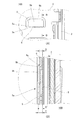
放熱板(第2の部品)5は、背面カバー4に対して本体内側から組み付く構成になっている。本実施形態において、放熱板5の材質は、導電性を有する金属の放熱部材であり、プレス加工等によって所望の形状に加工されている。背面カバー4に放熱板5と、サブシャーシ7を位置合わせした後、ビス8a、8b及び8cを背面カバー4に締結させることで、背面カバー4に対して放熱板5及びサブシャーシ7が固定される。
The heat radiating plate (second component) 5 is assembled to the back cover 4 from the inside of the main body. In the present embodiment, the
背面カバーユニット50の組み立てが完了した状態において、表示ユニット3の本体内側平面と放熱板5の本体外側平面との間には一定の隙間が確保されている。放熱板5には、予めガスケット(導電性弾性体)6が貼り付けられている。ガスケット6は、弾性を有するポリウレタン等の素材に導電性を有する素材、例えば、導電布等を巻き付けた複合部材である。本実施形態では、ガスケット6は、放熱板5に対して、導電性を有する両面テープで貼り付けられている。ガスケット6は、表示ユニット3の本体内側平面と放熱板5の本体外側平面との間に形成される隙間よりも大きい厚みを有している。背面カバー4に固定されるとガスケット6は、金属カバー3cと放熱板5との間で押圧されて金属カバー3cと放熱板5を電気的に接続する構成になっている。
In a state where the assembly of the
図3は、背面カバーユニット50におけるガスケット6が配置される領域の概略図及び断面図である。図3(B)は、図3(A)中の矢視A−A断面図である。開口部(第2の開口部)5aは、放熱板5に形成された開口部である。開口部5aの周縁部の一部には、段差部5bが形成されている。段差部5bは、表示ユニット3から離間する方向に突出した段差形状を有しており、放熱板5に対して絞り加工または半抜き加工等を施すことによって形成される。放熱板5は、段差部5bを形成することによって、段差部5bと表示ユニット3との間に隙間部5cが形成される。ガスケット6の一部は、隙間部5cに配設されて、段差部5bにおける表示ユニット3側平面に貼り付けられて保持されている。
FIG. 3 is a schematic view and a cross-sectional view of a region where the
さらに、ガスケット6の一部は段差部5bから開口部5a側(第2の開口部側)に延出している。ガスケット6は、段差部5bの表示ユニット3側平面と表示ユニット3の放熱板5側平面との距離Dよりも大きい厚みTを有している。ガスケット6を貼り付けた放熱板5を背面カバーに組み付けると、隙間部5cにおけるガスケット6は、厚みTと距離Dの差分だけ押圧されて保持される。ガスケット6は、表示ユニット3の金属カバー3cと放熱板5との間で押圧(圧接)されて保持されることで電気的接続を安定的に維持することができる。
Furthermore, a part of the
図4は、背面カバーユニット50を本体1に組み込む状態を表す斜視図である。本体1は、メインシャーシ(第1の部品)9及び制御基板10を有する。メインシャーシ9は、導電性を有する金属で構成され、本体1を構成する不図示の各ユニットを保持している。図4では便宜上、本体1を構成する部品の内、メインシャーシ9及び制御基板10以外の部品を省略し、本体1の外形を2点鎖線で模式的に示す。メインシャーシ9には、複数の締結部が形成されている。
FIG. 4 is a perspective view illustrating a state in which the
制御基板10は、他の機構部品とともにメインシャーシ9に組み付けられている。制御基板10のグランド配線パターンの一部は、導体が露出しており、メインシャーシ9の締結部と当接するように構成されている。メインシャーシ9に組み付けられることで制御基板10のグランド配線パターンは、メインシャーシ9と電気的に接続される。締結部9aは、複数の締結部の内の1つであり、締結部9aにはバーリング加工等によって立ち上げられた穴部が形成されている。そして、穴部の内側面には、タップ加工が施されて、ビスが締結可能になっている。
The
一方、背面カバーユニット50には複数の締結部が形成されている。締結部50aは、複数の締結部の内の一つであり、締結部50aには貫通穴が形成されている。背面カバーユニット50を本体1に組み込むと、締結部50aは、締結部9aの穴部と締結部50aの穴部の中心が同軸上に位置する。このとき、締結部50aは、締結部9aよりも本体外側に位置している。
On the other hand, the
背面カバーユニット50の組み込みが完了すると、背面カバーユニット50は、ビスによって不図示の外装カバー等とともにメインシャーシ9に固定される。次に、メインシャーシ9には、開口部(第1の開口部)9bが形成されている。開口部9bは、放熱板5に形成されている段差部5bよりも大きい開口である。背面カバーユニット50を本体1に組み込むと、段差部5bが開口部9bの内側に入り込むように(挿入されるように)開口部9bの位置が設定されている。なお、メインシャーシ9に形成されている開口部9bは、導電性を有する領域に形成されていればよい。
When the assembly of the
図5は、撮像装置100におけるガスケット6が配置される領域の概略図及び断面図である。図5(B)は、図5(A)中の矢視B−B断面図である。放熱板5は、背面カバーユニット50を本体1に組み込むと、段差部5bの表示ユニット3側平面とメインシャーシ9の表示ユニット3側平面がほぼ同一平面上になるように配置される。従って、開口部5aを覆う領域におけるメインシャーシ9の表示ユニット3側平面と表示ユニット3の放熱板5側平面との距離D’は、段差部5bの表示ユニット3側平面と表示ユニット3の放熱板5側平面との距離Dとほぼ同じ距離になる。背面カバーユニット50を本体1に組み込むと、段差部5bから開口部5a側に延出しているガスケット6の一部は、厚みTと距離D’の差分だけ押圧されて保持される。
FIG. 5 is a schematic view and a cross-sectional view of a region where the
ガスケット6は、金属カバー3cとメインシャーシ9との間で押圧されて金属カバー3cとメインシャーシ9を電気的に接続することができる。また、前述の通りガスケット6は金属カバー3cと放熱板5を電気的に接続しているため、ガスケット6によって金属カバー3cと、放熱板5と、メインシャーシ9との3つの部品に対して同時に電気的接続をとることができる。段差部5bの表示ユニット3側平面は、メインシャーシ9の表示ユニット3側平面とほぼ同一平面上になるように配置される。そのため、ガスケット6を偏りなく均一に押圧することができる。
The
従って、導電性を有する複数の部品に対して電気的接続を安定的に確保することができる。また、放熱板5の板厚は、メインシャーシ9の板厚と同等、またはメインシャーシ9の板厚よりも薄くなるように設定されている。段差部5bの表示ユニット3側平面とメインシャーシ9の表示ユニット3側平面がほぼ同一平面上になるように配置されるため、段差部5bのメインシャーシ9側平面は、メインシャーシ9の板厚の範囲内に収まるように構成されている。従って、メインシャーシ9の板厚方向に対する撮像装置100の厚みを増大することなく、導電性を有する複数の部品に対して電気的接続をとることができる。
Therefore, it is possible to stably ensure electrical connection to a plurality of conductive parts. The plate thickness of the
なお、本実施形態では、導電性を有する両面テープで、ガスケット6を放熱板5に対して貼り付けている。ガスケット6をメインシャーシ9に貼り付ける場合、背面カバーユニット50を本体1に組み付ける際、ガスケット6の一部を隙間部5cに挿入しながら組み付ける作用になるため、組み付け作業が非常に困難になってしまう。また、ガスケット6を金属カバー3cに組み付ける場合、ガスケット6が隙間部5cの内部に収まるようにガスケット6を貼り付ける位置を精度よく規定する目印が必要になる。例えば、金属カバー3cに対して、ケガキ線を設ける、枠線印刷を施す等の加工が必要になり、表示ユニット3の製造コストが増大してしまう虞がある。これらに対して、ガスケット6を放熱板5に貼り付ける場合、ガスケット6は、段差部5bに対してガスケット6の一部が開口部5a側に延出するように貼り付ければよく、新たに目印を設けることなく容易に精度良くガスケットを所望の位置に貼り付けることができる。従って、ガスケット6は放熱板5に貼り付けることが望ましい。
In the present embodiment, the
図6は、表示ユニット3を示す平面図である。図6(A)は、図6(B)に示す表示ユニット3の側面図である。なお、本実施形態に係る表示ユニット3として、液晶ディスプレイモジュールとタッチパネルモジュールを組み合わせたユニットを用いて説明する。ただし、本実施形態に係る電子機器は、これに限定されるものではなく、例えば、本体1に内蔵された不図示の制御基板から出力された画像信号等を表示することができる表示装置に広く適用することができる。
FIG. 6 is a plan view showing the
表示ユニット3は、バックライトモジュール30、液晶ディスプレイ31及びタッチパネル32と、フレキシブルプリント基板3a、3bで構成されている。バックライトモジュール30、液晶ディスプレイ31及びタッチパネル32は、それぞれ重ねて接合し、一体化された状態でユニット化されている。バックライトモジュール30には、金属カバー3cが含まれている。フレキシブルプリント基板3bは、バックライトモジュール30に接続されている。フレキシブルプリント基板3aは、液晶ディスプレイ31及びタッチパネル32に接続されている。フレキシブルプリント基板3a及び3bは、前述の通り、本体1に組み込まれると、不図示の制御基板に接続される構成になっている。表示領域3dは、表示ユニット3の表示領域である。領域3eは、液晶ディスプレイ駆動ICが実装されている領域(以下、IC実装部と称する)である。液晶ディスプレイ31は、内部に不図示のガラス基板を含み、ガラス基板には複数の電極端子が形成されている。IC実装部3eは、この電極端子にCOG(Chip On Glass)方式等によって接続されている。
The
例えば、撮像装置100の操作によって長時間にわたり表示ユニット3に対して画像表示等が行われる場合がある。このとき、IC実装部3eに対する負荷が増加し、ICの自己発熱量が増加する。このICの発熱により、IC実装部3e及びその近傍付近と、液晶ディスプレイ31のIC実装部3e近傍以外の領域との間では、温度差が発生する。この影響により液晶ディスプレイ31の特性が部分的に変化し、結果として表示ムラ等の表示品位低下を招くことに繋がる。
For example, an image display or the like may be performed on the
そこで、本実施形態に係る撮像装置100は、放熱板5を表示ユニット3と向かい合う位置に近接して配置することで、IC実装部3eの発熱を放熱板5の広域にわたって拡散させる。これにより、液晶ディスプレイ31内の温度差を低減し、表示ムラ等の表示品位低下を低減させている。図6(B)において、2点鎖線で示される領域Pは、背面カバーユニット50の状態においてガスケット6が配置される領域を示している。ガスケット6は、IC実装部3eから離れた位置に設定されている。これにより、放熱板5の開口部5a及び段差部5bもIC実装部3eから離れた位置に形成されている。仮に、IC実装部3e近傍において放熱板5の開口部5a及び段差部5bが形成されると、IC実装部3eで発生する熱が放熱板5に伝熱しにくくなってしまう。
Therefore, the
従って、ガスケット6をIC実装部3eから離れた位置に設定することによって、IC実装部3eで発生する発熱をより効率的に放熱板5に伝熱させることができる。以上、本実施形態によれば、電子機器本体の小型化を阻害することなく導電性を有する複数の部品に対して電気的接続が可能な電子機器を提供することができる。
Therefore, by setting the
(第2実施形態)
以下、図7を参照して、本実施形態に係るメインシャーシ9の変形例であるメインシャーシ90について説明する。メインシャーシ90が適用される撮像装置におけるメインシャーシ90以外の構成要素は、第1実施形態で説明した撮像装置100におけるメインシャーシ9以外の構成要素と同じであるため、本実施形態での説明を省略する。
(Second Embodiment)
Hereinafter, a main chassis 90 which is a modification of the
図7は、本実施形態に係るメインシャーシ90を備えた撮像装置100の断面図である。背面カバーユニット50を本体1に組み込むと、段差部5bの本体1側平面は、メインシャーシ90の本体1側平面に対して表示ユニット3に向かう方向に距離Xの隙間を確保するように配置されている。距離Xの隙間を確保することによって、背面カバーユニット50を組み込んだ後、段差部5bの本体1側平面が、メインシャーシ90の本体1側平面よりも本体1側に突出しないように構成されている。この距離Xは、各部品の加工公差や組み立て誤差等を考慮して決定される。
FIG. 7 is a cross-sectional view of the
このようにして、段差部5bと表示ユニット3との間に隙間部5cを形成し、ガスケット6は、隙間部5cに配置される。放熱板5の板厚は、メインシャーシ90の板厚と同等、またはメインシャーシ90の板厚よりも厚くなるように設定されている。メインシャーシ90は、ガスケット6と接する範囲に対して突出部90cを形成している。突出部90cは、表示ユニット3に向かう方向に突出した突出形状を有しており、メインシャーシ90に対して絞り加工または半抜き加工等を施すことによって形成される。
In this way, the
突出部90cの表示ユニット3側平面と表示ユニット3の放熱板5側平面との距離E’は、段差部5bの表示ユニット3側平面と表示ユニット3の放熱板5側平面との距離Eとほぼ同じ距離になるように突出部90cの突出量が設定されている。ガスケット6は、前述の通り、金属カバー3cと放熱板5を電気的に接続しているため、ガスケット6によって金属カバー3cと、放熱板5と、メインシャーシ90との3つの部品に対して同時に電気的接続をとることができる。また、ガスケット6を偏りなく均一に押圧し、導電性を有する複数の部品に対して電気的接続を安定的に確保することができる。そして、メインシャーシ90の板厚方向に対する撮像装置100の厚みを増大することなく、導電性を有する複数の部品に対して電気的接続をとることができる。
The distance E ′ between the
以上、本実施形態によれば、電子機器本体の小型化を阻害することなく導電性を有する複数の部品に対して電気的接続が可能な電子機器を提供することができる。なお、本実施形態では、3つの部品に対して同時に電気的接続を可能にする構成について説明した。しかしながら、同時に電気的接続をとる部品の点数は、3つに限定されることはなく、4つ以上の部品に対して同時に電気的接続を可能にする構成であってもよい。また、複数の部品に対して同時に電気的接続を可能にする部品の一例としてガスケットを取り上げているが、これに限定することなく、例えば、弾性を有する部品として、導電性を有する材料を加工して得られるコイルバネや板バネ等を採用してもよい。 As described above, according to this embodiment, it is possible to provide an electronic device that can be electrically connected to a plurality of conductive parts without hindering downsizing of the electronic device main body. In the present embodiment, the configuration that enables electrical connection to three components simultaneously has been described. However, the number of parts that can be electrically connected at the same time is not limited to three, and it may be a configuration that enables simultaneous electrical connection to four or more parts. In addition, a gasket is taken up as an example of a component that enables electrical connection to a plurality of components at the same time. However, the present invention is not limited to this. For example, a material having conductivity is processed as an elastic component. A coil spring, a leaf spring, or the like obtained in this way may be employed.
また、本発明の好ましい実施形態について説明したが、本発明は、これらの実施形態に限定されず、その要旨の範囲内で種々の変形および変更が可能である。 Moreover, although preferable embodiment of this invention was described, this invention is not limited to these embodiment, A various deformation | transformation and change are possible within the range of the summary.
3 表示ユニット(第3の部品)
5 放熱板(第2の部品)
5a 開口部(第2の開口部)
5b 段差部
6 ガスケット(導電性弾性体)
9 メインシャーシ(第1の部品)
9b 開口部(第1の開口部)
3 Display unit (third part)
5 Heat sink (second part)
5a Opening (second opening)
9 Main chassis (first part)
9b opening (first opening)
Claims (8)
導電性を有する領域を含み、前記導電性を有する領域に第2の開口部と、前記第2の開口部に一部が接する段差部を有する第2の部品と、
導電性を有する領域を含む第3の部品と、
弾性を有し、導電性を有する領域を含む導電性弾性体と、
を備え、
前記第2の部品は、前記段差部が前記第1の開口部に挿入されるように、前記第1の部品と前記第3の部品との間に配され、
前記導電性弾性体は、その一部が前記段差部から前記第2の開口部側に延出し、前記第1の部品と、前記段差部と、前記第3の部品との間で圧接されて保持される
ことを特徴とする電子機器。 A first component including a region having conductivity, and having a first opening in the region having conductivity;
A second part including a region having conductivity, a second opening in the region having conductivity, and a step part partially in contact with the second opening;
A third part including a region having conductivity;
A conductive elastic body having elasticity and including a conductive region;
With
The second component is disposed between the first component and the third component such that the stepped portion is inserted into the first opening.
A part of the conductive elastic body extends from the stepped portion toward the second opening, and is pressed between the first component, the stepped portion, and the third component. An electronic device characterized by being held.
ことを特徴とする請求項1に記載の電子機器。 The electronic apparatus according to claim 1, wherein the conductive elastic body is fixed to the second component by being attached with a double-sided tape having conductivity.
ことを特徴とする請求項1または2に記載の電子機器。 In the direction in which the conductive elastic body is in pressure contact, the distance between the region where the stepped portion is in contact with the conductive elastic body and the third component is such that the first component is connected to the conductive elastic body. 3. The electronic device according to claim 1, wherein the step of the step portion is set to be the same as a distance between a contact area and the third component.
ことを特徴とする請求項1〜3のいずれか1項に記載の電子機器。 The first part has a protruding part that protrudes in a direction toward the third part with respect to a range including a region in contact with the conductive elastic body or a part thereof. 4. The electronic device according to any one of items 3.
ことを特徴とする請求項4に記載の電子機器。 In the direction in which the conductive elastic body is pressure-contacted, the distance between the protrusion and the third part is the same as the distance between the step and the third part. The electronic device according to claim 4, wherein an amount of protrusion is set.
前記導電性弾性体は、前記発熱源と重なる領域から離れた位置に配置される
ことを特徴とする請求項1〜5のいずれか1項に記載の電子機器。 At least one of the first component, the second component, and the third component has a region serving as a heat source inside,
The electronic apparatus according to claim 1, wherein the conductive elastic body is disposed at a position away from a region overlapping with the heat generation source.
をさらに備え、
前記第1の部品は、前記制御基板が固定されるメインシャーシであり、前記第2の部品は、前記電子機器の内部に配設される放熱部材であり、前記第3の部品は、前記制御基板から出力された情報を表示する表示装置である
ことを特徴とする請求項1〜6のいずれか1項に記載の電子機器。 It further includes a control board on which electronic components are mounted,
The first component is a main chassis to which the control board is fixed, the second component is a heat dissipating member disposed inside the electronic device, and the third component is the control The electronic apparatus according to claim 1, wherein the electronic apparatus is a display device that displays information output from a substrate.
Priority Applications (1)
| Application Number | Priority Date | Filing Date | Title |
|---|---|---|---|
| JP2016000199A JP6628608B2 (en) | 2016-01-04 | 2016-01-04 | Electronic equipment and imaging device |
Applications Claiming Priority (1)
| Application Number | Priority Date | Filing Date | Title |
|---|---|---|---|
| JP2016000199A JP6628608B2 (en) | 2016-01-04 | 2016-01-04 | Electronic equipment and imaging device |
Publications (3)
| Publication Number | Publication Date |
|---|---|
| JP2017122756A true JP2017122756A (en) | 2017-07-13 |
| JP2017122756A5 JP2017122756A5 (en) | 2019-02-14 |
| JP6628608B2 JP6628608B2 (en) | 2020-01-08 |
Family
ID=59306821
Family Applications (1)
| Application Number | Title | Priority Date | Filing Date |
|---|---|---|---|
| JP2016000199A Active JP6628608B2 (en) | 2016-01-04 | 2016-01-04 | Electronic equipment and imaging device |
Country Status (1)
| Country | Link |
|---|---|
| JP (1) | JP6628608B2 (en) |
Citations (9)
| Publication number | Priority date | Publication date | Assignee | Title |
|---|---|---|---|---|
| JP2003204457A (en) * | 2001-10-29 | 2003-07-18 | Olympus Optical Co Ltd | Imaging apparatus |
| JP2008026562A (en) * | 2006-07-20 | 2008-02-07 | Canon Inc | Imaging apparatus and imaging unit |
| US20110310564A1 (en) * | 2010-06-16 | 2011-12-22 | Canon Kabushiki Kaisha | Image pickup apparatus and electronic device |
| CN102823229A (en) * | 2011-01-31 | 2012-12-12 | 松下电器产业株式会社 | Imaging device |
| JP2013061395A (en) * | 2011-09-12 | 2013-04-04 | Canon Inc | Electronic apparatus |
| JP2014039163A (en) * | 2012-08-16 | 2014-02-27 | Nikon Corp | Electronic apparatus |
| JP2014099558A (en) * | 2012-11-15 | 2014-05-29 | Toshiba Corp | Grounding gasket and electronic apparatus |
| JP2014179515A (en) * | 2013-03-15 | 2014-09-25 | Mitsubishi Electric Corp | Electronic apparatus |
| JP2014225609A (en) * | 2013-05-17 | 2014-12-04 | キヤノン株式会社 | Electronic apparatus |
-
2016
- 2016-01-04 JP JP2016000199A patent/JP6628608B2/en active Active
Patent Citations (9)
| Publication number | Priority date | Publication date | Assignee | Title |
|---|---|---|---|---|
| JP2003204457A (en) * | 2001-10-29 | 2003-07-18 | Olympus Optical Co Ltd | Imaging apparatus |
| JP2008026562A (en) * | 2006-07-20 | 2008-02-07 | Canon Inc | Imaging apparatus and imaging unit |
| US20110310564A1 (en) * | 2010-06-16 | 2011-12-22 | Canon Kabushiki Kaisha | Image pickup apparatus and electronic device |
| CN102823229A (en) * | 2011-01-31 | 2012-12-12 | 松下电器产业株式会社 | Imaging device |
| JP2013061395A (en) * | 2011-09-12 | 2013-04-04 | Canon Inc | Electronic apparatus |
| JP2014039163A (en) * | 2012-08-16 | 2014-02-27 | Nikon Corp | Electronic apparatus |
| JP2014099558A (en) * | 2012-11-15 | 2014-05-29 | Toshiba Corp | Grounding gasket and electronic apparatus |
| JP2014179515A (en) * | 2013-03-15 | 2014-09-25 | Mitsubishi Electric Corp | Electronic apparatus |
| JP2014225609A (en) * | 2013-05-17 | 2014-12-04 | キヤノン株式会社 | Electronic apparatus |
Also Published As
| Publication number | Publication date |
|---|---|
| JP6628608B2 (en) | 2020-01-08 |
Similar Documents
| Publication | Publication Date | Title |
|---|---|---|
| US7633543B2 (en) | Solid state imaging apparatus | |
| JP4668036B2 (en) | Mounting structure for FPC of image sensor | |
| GB2413435A (en) | Camera lens module and method of assembly thereof | |
| EP3706405B1 (en) | Image capture module of electronic device | |
| US11895793B2 (en) | Image pickup unit and imaging apparatus | |
| JP2006345196A (en) | Holding structure for solid-state imaging element | |
| US11317027B2 (en) | Imaging unit and imaging apparatus | |
| JP4767778B2 (en) | Flexible substrate and photographing apparatus | |
| JP2013016894A (en) | Solid-state imaging device and manufacturing method of the same | |
| JP2011233837A (en) | Optical transceiver | |
| US20060055812A1 (en) | Optical equipment having image pickup element | |
| TWI666504B (en) | Lens driving apparatus, photographing module and electronic device | |
| JP2020108004A (en) | Electronic device heat dissipation structure and heat dissipation method | |
| JP6628608B2 (en) | Electronic equipment and imaging device | |
| JP5464930B2 (en) | Electronics | |
| JP7406314B2 (en) | electronic modules and equipment | |
| KR100947967B1 (en) | Camera module and manufacturing method thereof | |
| JP2009260863A (en) | Substrate grounding structure for preventing sensitivity suppression, method, and mobile phone | |
| JP5188412B2 (en) | Imaging apparatus and electronic apparatus | |
| JP2015045757A (en) | Electronic equipment | |
| JP2019192813A (en) | Electronic apparatus and method of manufacturing the same | |
| JP5805114B2 (en) | Imaging apparatus and electronic apparatus | |
| JP6547874B2 (en) | Electronics | |
| CN113543457A (en) | Image pickup unit and image pickup apparatus | |
| US20190271904A1 (en) | Accessory shoe device capable of preventing fall-off of fastening screw by saving space, and electronic apparatus |
Legal Events
| Date | Code | Title | Description |
|---|---|---|---|
| A521 | Request for written amendment filed |
Free format text: JAPANESE INTERMEDIATE CODE: A523 Effective date: 20181221 |
|
| A621 | Written request for application examination |
Free format text: JAPANESE INTERMEDIATE CODE: A621 Effective date: 20181221 |
|
| A977 | Report on retrieval |
Free format text: JAPANESE INTERMEDIATE CODE: A971007 Effective date: 20191021 |
|
| TRDD | Decision of grant or rejection written | ||
| A01 | Written decision to grant a patent or to grant a registration (utility model) |
Free format text: JAPANESE INTERMEDIATE CODE: A01 Effective date: 20191105 |
|
| A61 | First payment of annual fees (during grant procedure) |
Free format text: JAPANESE INTERMEDIATE CODE: A61 Effective date: 20191203 |
|
| R151 | Written notification of patent or utility model registration |
Ref document number: 6628608 Country of ref document: JP Free format text: JAPANESE INTERMEDIATE CODE: R151 |